KR101050868B1 - LCD Display - Google Patents
LCD DisplayDownload PDFInfo
- Publication number
- KR101050868B1 KR101050868B1KR1020040022446AKR20040022446AKR101050868B1KR 101050868 B1KR101050868 B1KR 101050868B1KR 1020040022446 AKR1020040022446 AKR 1020040022446AKR 20040022446 AKR20040022446 AKR 20040022446AKR 101050868 B1KR101050868 B1KR 101050868B1
- Authority
- KR
- South Korea
- Prior art keywords
- liquid crystal
- inverter
- cover
- crystal panel
- protective cover
- Prior art date
- Legal status (The legal status is an assumption and is not a legal conclusion. Google has not performed a legal analysis and makes no representation as to the accuracy of the status listed.)
- Expired - Lifetime
Links
Images


Classifications
- G—PHYSICS
- G02—OPTICS
- G02F—OPTICAL DEVICES OR ARRANGEMENTS FOR THE CONTROL OF LIGHT BY MODIFICATION OF THE OPTICAL PROPERTIES OF THE MEDIA OF THE ELEMENTS INVOLVED THEREIN; NON-LINEAR OPTICS; FREQUENCY-CHANGING OF LIGHT; OPTICAL LOGIC ELEMENTS; OPTICAL ANALOGUE/DIGITAL CONVERTERS
- G02F1/00—Devices or arrangements for the control of the intensity, colour, phase, polarisation or direction of light arriving from an independent light source, e.g. switching, gating or modulating; Non-linear optics
- G02F1/01—Devices or arrangements for the control of the intensity, colour, phase, polarisation or direction of light arriving from an independent light source, e.g. switching, gating or modulating; Non-linear optics for the control of the intensity, phase, polarisation or colour
- G02F1/13—Devices or arrangements for the control of the intensity, colour, phase, polarisation or direction of light arriving from an independent light source, e.g. switching, gating or modulating; Non-linear optics for the control of the intensity, phase, polarisation or colour based on liquid crystals, e.g. single liquid crystal display cells
- G02F1/133—Constructional arrangements; Operation of liquid crystal cells; Circuit arrangements
- G02F1/1333—Constructional arrangements; Manufacturing methods
- G02F1/1335—Structural association of cells with optical devices, e.g. polarisers or reflectors
- G02F1/1336—Illuminating devices
- G02F1/133602—Direct backlight
- G02F1/133608—Direct backlight including particular frames or supporting means
- G—PHYSICS
- G02—OPTICS
- G02F—OPTICAL DEVICES OR ARRANGEMENTS FOR THE CONTROL OF LIGHT BY MODIFICATION OF THE OPTICAL PROPERTIES OF THE MEDIA OF THE ELEMENTS INVOLVED THEREIN; NON-LINEAR OPTICS; FREQUENCY-CHANGING OF LIGHT; OPTICAL LOGIC ELEMENTS; OPTICAL ANALOGUE/DIGITAL CONVERTERS
- G02F1/00—Devices or arrangements for the control of the intensity, colour, phase, polarisation or direction of light arriving from an independent light source, e.g. switching, gating or modulating; Non-linear optics
- G02F1/01—Devices or arrangements for the control of the intensity, colour, phase, polarisation or direction of light arriving from an independent light source, e.g. switching, gating or modulating; Non-linear optics for the control of the intensity, phase, polarisation or colour
- G02F1/13—Devices or arrangements for the control of the intensity, colour, phase, polarisation or direction of light arriving from an independent light source, e.g. switching, gating or modulating; Non-linear optics for the control of the intensity, phase, polarisation or colour based on liquid crystals, e.g. single liquid crystal display cells
- G02F1/133—Constructional arrangements; Operation of liquid crystal cells; Circuit arrangements
- G02F1/1333—Constructional arrangements; Manufacturing methods
- G02F1/133308—Support structures for LCD panels, e.g. frames or bezels
- G—PHYSICS
- G02—OPTICS
- G02F—OPTICAL DEVICES OR ARRANGEMENTS FOR THE CONTROL OF LIGHT BY MODIFICATION OF THE OPTICAL PROPERTIES OF THE MEDIA OF THE ELEMENTS INVOLVED THEREIN; NON-LINEAR OPTICS; FREQUENCY-CHANGING OF LIGHT; OPTICAL LOGIC ELEMENTS; OPTICAL ANALOGUE/DIGITAL CONVERTERS
- G02F1/00—Devices or arrangements for the control of the intensity, colour, phase, polarisation or direction of light arriving from an independent light source, e.g. switching, gating or modulating; Non-linear optics
- G02F1/01—Devices or arrangements for the control of the intensity, colour, phase, polarisation or direction of light arriving from an independent light source, e.g. switching, gating or modulating; Non-linear optics for the control of the intensity, phase, polarisation or colour
- G02F1/13—Devices or arrangements for the control of the intensity, colour, phase, polarisation or direction of light arriving from an independent light source, e.g. switching, gating or modulating; Non-linear optics for the control of the intensity, phase, polarisation or colour based on liquid crystals, e.g. single liquid crystal display cells
- G02F1/133—Constructional arrangements; Operation of liquid crystal cells; Circuit arrangements
- G02F1/1333—Constructional arrangements; Manufacturing methods
- G02F1/1335—Structural association of cells with optical devices, e.g. polarisers or reflectors
- G02F1/1336—Illuminating devices
- G02F1/133615—Edge-illuminating devices, i.e. illuminating from the side
- G—PHYSICS
- G02—OPTICS
- G02F—OPTICAL DEVICES OR ARRANGEMENTS FOR THE CONTROL OF LIGHT BY MODIFICATION OF THE OPTICAL PROPERTIES OF THE MEDIA OF THE ELEMENTS INVOLVED THEREIN; NON-LINEAR OPTICS; FREQUENCY-CHANGING OF LIGHT; OPTICAL LOGIC ELEMENTS; OPTICAL ANALOGUE/DIGITAL CONVERTERS
- G02F1/00—Devices or arrangements for the control of the intensity, colour, phase, polarisation or direction of light arriving from an independent light source, e.g. switching, gating or modulating; Non-linear optics
- G02F1/01—Devices or arrangements for the control of the intensity, colour, phase, polarisation or direction of light arriving from an independent light source, e.g. switching, gating or modulating; Non-linear optics for the control of the intensity, phase, polarisation or colour
- G02F1/13—Devices or arrangements for the control of the intensity, colour, phase, polarisation or direction of light arriving from an independent light source, e.g. switching, gating or modulating; Non-linear optics for the control of the intensity, phase, polarisation or colour based on liquid crystals, e.g. single liquid crystal display cells
- G02F1/133—Constructional arrangements; Operation of liquid crystal cells; Circuit arrangements
- G02F1/1333—Constructional arrangements; Manufacturing methods
- G02F1/1345—Conductors connecting electrodes to cell terminals
- G—PHYSICS
- G02—OPTICS
- G02F—OPTICAL DEVICES OR ARRANGEMENTS FOR THE CONTROL OF LIGHT BY MODIFICATION OF THE OPTICAL PROPERTIES OF THE MEDIA OF THE ELEMENTS INVOLVED THEREIN; NON-LINEAR OPTICS; FREQUENCY-CHANGING OF LIGHT; OPTICAL LOGIC ELEMENTS; OPTICAL ANALOGUE/DIGITAL CONVERTERS
- G02F1/00—Devices or arrangements for the control of the intensity, colour, phase, polarisation or direction of light arriving from an independent light source, e.g. switching, gating or modulating; Non-linear optics
- G02F1/01—Devices or arrangements for the control of the intensity, colour, phase, polarisation or direction of light arriving from an independent light source, e.g. switching, gating or modulating; Non-linear optics for the control of the intensity, phase, polarisation or colour
- G02F1/13—Devices or arrangements for the control of the intensity, colour, phase, polarisation or direction of light arriving from an independent light source, e.g. switching, gating or modulating; Non-linear optics for the control of the intensity, phase, polarisation or colour based on liquid crystals, e.g. single liquid crystal display cells
- G02F1/133—Constructional arrangements; Operation of liquid crystal cells; Circuit arrangements
- G02F1/1333—Constructional arrangements; Manufacturing methods
- G02F1/1335—Structural association of cells with optical devices, e.g. polarisers or reflectors
- G02F1/1336—Illuminating devices
- G02F1/133628—Illuminating devices with cooling means
Landscapes
- Physics & Mathematics (AREA)
- Nonlinear Science (AREA)
- Mathematical Physics (AREA)
- Chemical & Material Sciences (AREA)
- Crystallography & Structural Chemistry (AREA)
- General Physics & Mathematics (AREA)
- Optics & Photonics (AREA)
- Liquid Crystal (AREA)
Abstract
Translated fromKoreanDescription
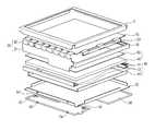
Translated fromKorean도1은 액정표시장치의 분해 사시도.1 is an exploded perspective view of a liquid crystal display device;
도2는 절연커버 및 금속커버가 부착된 액정표시장치의 배면을 나타낸 도면.2 is a rear view of a liquid crystal display device having an insulating cover and a metal cover attached thereto.
도3은 도2에서 결합된 형태의 액정표시장치를 분해하여 보인 분해사시도.3 is an exploded perspective view showing an exploded view of the liquid crystal display of the combined type in FIG.
도4는 본 발명에 따른 액정표시장치의 배면을 나타낸 도면.4 is a rear view of the liquid crystal display device according to the present invention;
도5는 본 발명에 따른 보호덮개의 전개도.5 is an exploded view of a protective cover according to the present invention.
***도면의 주요 부분에 대한 부호의 설명****** Description of the symbols for the main parts of the drawings ***
350: 메인 지지대352: 하부커버350: main support 352: lower cover
353: 커버 실드367: 보호덮개353: cover shield 367: protective cover
370: 인버터372: 소자370: inverter 372: device
379: 제 3결합부380: 지지부379: third coupling portion 380: support portion
본 발명은 액정표시장치(liquid crystal display device)에 관한 것으로서, 보다 자세하게는 대체된 인버터 커버(inverter cover)를 적용하여, 제작비용을 절감할 수 있도록 한 액정표시장치에 관한 것이다.BACKGROUND OF THE INVENTION 1. Field of the Invention The present invention relates to a liquid crystal display device, and more particularly, to a liquid crystal display device which can reduce manufacturing costs by applying an replaced inverter cover.
일반적으로, 액정표시장치는 매트릭스(matrix) 형태로 배열된 화소들에 화상정보에 따른 데이터신호를 개별적으로 공급하여, 그 화소들의 광투과율을 조절함으로써, 원하는 화상을 표시할 수 있도록 한 평판표시장치이다.In general, a liquid crystal display device is a flat panel display device that can display a desired image by separately supplying data signals according to image information to pixels arranged in a matrix form, and adjusting light transmittance of the pixels. to be.
따라서, 액정표시장치에는 화소들이 매트릭스 형태로 배열되는 액정패널과; 상기 화소들을 구동하기 위한 구동부가 구비된다.Accordingly, the LCD device includes a liquid crystal panel in which pixels are arranged in a matrix; A driving unit for driving the pixels is provided.
상기 액정패널은 서로 대향하여 동일한 셀-갭(cell-gap)이 유지되도록 합착된 박막 트랜지스터 어레이(thin film transistor array) 기판 및 컬러필터(color filter) 기판과, 그 컬러필터 기판 및 박막 트랜지스터 어레이 기판의 셀-갭에 형성된 액정층으로 구성된다.The liquid crystal panel includes a thin film transistor array substrate and a color filter substrate bonded together so that the same cell-gap is maintained to face each other, and the color filter substrate and the thin film transistor array substrate. It consists of a liquid crystal layer formed in the cell-gap of.
상기 액정 표시장치는 자체적으로 발광하지 못하고, 빛의 투과율을 조절하여 화상을 표시하는 특성을 갖기 때문에 액정패널에 빛을 조사하기 위한 별도의 장치, 즉 백라이트 유닛이 요구된다.Since the liquid crystal display does not emit light by itself and has a characteristic of displaying an image by adjusting light transmittance, a separate device for irradiating light to the liquid crystal panel, that is, a backlight unit, is required.
상기 백라이트 유닛은 램프가 액정패널의 배면에 배치되어 빛이 액정패널의 전면에 직접 투과되도록 하는 직하 방식과, 램프가 액정패널의 일측면 또는 양측면에 배치되어, 빛이 도광판, 반사판 및 광학시트들을 통해 반사, 확산 및 집광됨으로써, 액정패널의 전면에 투과되도록 하는 에지(edge) 방식으로 구분된다.The backlight unit includes a lamp disposed on a rear surface of the liquid crystal panel so that light is transmitted directly to the front surface of the liquid crystal panel, and a lamp is disposed on one side or both sides of the liquid crystal panel so that the light is disposed on the light guide plate, the reflecting plate and the optical sheets. By reflecting, diffusing and condensing through, it is divided into an edge (edge) method to be transmitted to the front of the liquid crystal panel.
상기한 바와같이 액정 표시장치는 액정패널, 구동부 및 백라이트 유닛으로 구성되며, 이와같은 액정패널, 구동부 및 백라이트 유닛을 지지 및 결합시키기 위하여 다양한 형태의 부품들이 사용된다.As described above, the liquid crystal display includes a liquid crystal panel, a driver, and a backlight unit, and various types of components are used to support and couple the liquid crystal panel, the driver, and the backlight unit.
상기한 바와 같은 액정표시장치를 첨부된 도면을 참조하여 상세하게 설명하 면 다음과 같다.The liquid crystal display as described above will be described in detail with reference to the accompanying drawings.
도1은 액정표시장치의 분해 사시도이다.1 is an exploded perspective view of a liquid crystal display device.
도1을 참조하면, 액정표시장치는 화소들이 매트릭스 형태로 배열되는 액정패널(10)과; 상기 액정패널(10)의 측면에 각각 접속된 게이트 구동부(20) 및 데이터 구동부(30)와; 상기 액정패널(10)의 배면에 배치된 백라이트 유닛(40)으로 구성된다.Referring to FIG. 1, a liquid crystal display device includes a
상기 액정패널(10)은 서로 대향하여 균일한 셀-갭이 유지되도록 합착된 박막 트랜지스터 어레이 기판 및 컬러필터 기판과, 그 컬러필터 기판 및 박막 트랜지스터 어레이 기판의 이격 간격에 형성된 액정층으로 구성된다.The
상기 박막 트랜지스터 어레이 기판과 컬러필터 기판이 합착된 액정패널(10)에는 공통전극과 화소전극이 형성되어 상기 액정층에 전계를 인가한다.A common electrode and a pixel electrode are formed in the
따라서, 상기 공통전극에 전압이 인가된 상태에서 상기 화소전극에 인가되는 데이터신호의 전압을 제어하게 되면, 상기 액정층의 액정은 상기 공통전극과 화소전극 사이의 전계에 따라 유전 이방성에 의해 회전함으로써, 화소별로 빛을 투과시키거나 차단시켜 문자나 화상을 표시하게 된다.Therefore, when the voltage of the data signal applied to the pixel electrode is controlled while the voltage is applied to the common electrode, the liquid crystal of the liquid crystal layer rotates by dielectric anisotropy according to the electric field between the common electrode and the pixel electrode. For example, characters or images are displayed by transmitting or blocking light for each pixel.
또한, 상기 화소전극에 인가되는 데이터신호의 전압을 화소별로 제어하기 위해서 박막 트랜지스터와 같은 스위칭소자가 화소들에 개별적으로 구비된다.In addition, switching elements such as thin film transistors are individually provided in the pixels in order to control the voltage of the data signal applied to the pixel electrode for each pixel.
상기 게이트 구동부(20)와 데이터 구동부(30)는 상기 액정패널(10)과 다양한 형태로 결합되어 액정패널(10)에 형성된 게이트 라인들 및 데이터 라인들에 주사신호와 화상정보를 공급함으로써, 액정패널(10)의 화소들을 구동시킨다.The gate driver 20 and the
상기 백라이트 유닛(40)은 상기 액정패널(10)의 배면에 배치된 도광판(41)과; 상기 도광판(41)의 양측면에 배치된 램프(42)와; 상기 램프(42)를 보호하고, 상기 램프(42)의 빛을 반사시키는 램프하우징(43)과, 상기 도광판(41)의 배면에 배치된 반사판(44)으로 구성되며, 상기 액정패널(10)과 도광판(41)의 사이에 광학시트(45)가 배치된다.The
상기 램프(42)에서 발생된 빛은 투명한 재질로 형성된 도광판(41)의 측면으로 입사된다.The light generated by the
상기 도광판(41)의 배면에 배치된 반사판(44)은 도광판(41)의 배면으로 투과되는 빛을 도광판(41)의 상면으로 반사시켜 빛의 손실을 줄이고, 도광판(41)의 상면으로 투과되는 빛의 균일도를 향상시킨다.The reflective plate 44 disposed on the rear surface of the
그리고, 상기 도광판(41)은 반사판(44)과 함께 램프(42)에서 발생된 빛을 상면으로 투과시킨다.The
한편, 상기 백라이트 유닛(40)은 도광판(41)의 양측면에 램프(42)가 구비된 에지 방식이 적용되었으나, 상기 도광판(41)의 일측면에만 램프가 구비된 에지 방식이 적용될 수 있으며, 또는 램프가 액정패널(10)의 배면 전체에 대응되도록 배치되는 직하 방식이 적용될 수 있다.On the other hand, the
상기 액정패널(10)과 백라이트 유닛(40)은 메인 지지대(50)에 적층되며, 그 적층된 액정패널(10)과 백라이트 유닛(40)의 측면이 메인 지지대(50)에 의해 지지된다.The
상기 액정패널(10)의 상면 가장자리는 상부 케이스(51)에 의해 압착되며, 그 상부 케이스(51)는 상기 메인 지지대(50)와 결합된다.The upper edge of the
상기 액정패널(10) 및 백라이트 유닛(40)은 백라이트 유닛(40)의 배면에 배치된 하부 커버(52)에 의해 지지되며, 그 하부 커버(52)는 상기 상부 케이스(51)와 결합된다.The
상기 데이터 구동부(30)에는 인쇄회로기판(31)이 구비되며, 그 인쇄회로기판(31)에는 상기 액정패널(10)의 화소들을 구동시키기 위한 각종 전기 신호들을 발생시키는 집적회로 칩들과, 그 전기 신호들을 전송하기 위한 배선들이 실장되기 때문에 일정한 면적이 요구된다.The
따라서, 상기 인쇄회로기판(31)은 상기 하부 커버(52)의 배면에 배치되고, 상기 액정패널(10)의 측면으로부터 상기 메인 지지대(50)의 측면을 타고 하부 커버(52)의 바닥면으로 절곡되는 가요성 도전필름(32)을 통해 상기 액정패널(10)과 접속된다.Accordingly, the printed
상기 하부 커버(52)의 바닥면에 배치된 인쇄회로기판(31)은 하부 커버(52)와 나사에 의해 결합되는 커버 실드(cover shield, 53)에 의해 보호된다.The printed
또한, 상기 백라이트 유닛을 구동하기 위해서는 램프에 구동전압을 공급하여야 하는데, 이러한 역할을 하는 것이 인버터(inverter)이다. 상기 인버터는 상기 인쇄회로기판으로부터 직류로 된 구동전압을 인가받아 교류로 전환한 다음, 램프를 충분히 구동시킬 수 있는 레벨의 전압으로 승압시켜 램프에 공급한다. 상기 인버터는 직류를 교류로 전환시킬 회로와 교류로 전환된 전압을 승압시킬 회로가 포함되어야 하므로, 일정한 면적이 요구된다. 따라서, 상기 하부커버의 배면에 구비되어 금속 커버(58)에 의해 보호된다.In addition, in order to drive the backlight unit, a driving voltage must be supplied to a lamp. An inverter plays such a role. The inverter receives a driving voltage of direct current from the printed circuit board, converts the current into an alternating current, and then boosts the lamp to a voltage that can sufficiently drive the lamp to supply the lamp. Since the inverter must include a circuit for converting direct current to alternating current and a circuit for boosting voltage converted to alternating current, a constant area is required. Therefore, it is provided on the rear surface of the lower cover and protected by the
상기 인버터에는 상기 램프를 구동시키기 위한 고전압이 형성되므로, 상기 인버터 부분이 외부에 노출될 경우 여러가지 전기사고를 유발할 수 있다. 따라서,상기 인버터의 상부를 덮어 외부와 절연상태를 만들기 위한 절연커버가 부착된다. 그런데, 상기 절연커버는 보통 얇은 비금속재질로 제작되어 있어 상기 인버터에 부착된 각종 소자들을 외부의 물리적 충격으로부터 보호해줄 수는 없으므로, 상기 절연커버 상에 또 하나의 커버인 금속커버를 구비한다.Since the high voltage for driving the lamp is formed in the inverter, when the inverter part is exposed to the outside, various electric accidents may be caused. Therefore, an insulation cover is attached to cover the upper portion of the inverter to make an insulation state with the outside. However, since the insulating cover is usually made of a thin non-metallic material, it is not possible to protect the various elements attached to the inverter from external physical shocks, so that the insulating cover has another metal cover on the insulating cover.
상기와 같은 각종 커버들이 부착된 일반적인 액정표시장치를 첨부된 도면을 참조하여 상세히 설명하면 다음과 같다.A general liquid crystal display device having the various covers as described above will be described in detail with reference to the accompanying drawings.
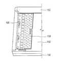
도2는 절연커버 및 금속커버가 부착된 액정표시장치의 배면을 나타낸 도면이다.FIG. 2 is a rear view of a liquid crystal display device having an insulating cover and a metal cover.
도면을 참조하면, 액정표시장치는 하부 커버에 부착되어 램프의 구동을 위한 전원을 공급하는 인버터와; 상기 인버터 상부에 구비되어 인버터를 외부와 절연시키는 절연커버와; 상기 절연커버 상부에 구비되어 상기 인버터를 외부의 물리적 충격으로부터 보호하는 금속커버(158)를 포함하여 구성된다.Referring to the drawings, the liquid crystal display device is attached to the lower cover and the inverter for supplying power for driving the lamp; An insulation cover provided above the inverter to insulate the inverter from the outside; A
상기 액정표시장치의 배면을 보면, 메인 지지대(150)의 하면을 하부 커버(152)가 보호 및 지지하며, 그 하부커버(152)의 일측에 인쇄회로기판을 보호하기 위한 커버실드(153)가 구비된다.Looking at the rear surface of the liquid crystal display, the
도면에 도시되진 않았지만, 상기 하부커버(152)의 타측에는 램프(미도시)에 전원을 공급하여, 상기 램프를 구동시키기 위한 인버터(미도시)가 일정한 면적에 걸쳐 부착되어 있다. 또한, 상기 인버터는 외부의 직류를 공급받아 교류로 변환한 다음 고전압의 전류로 승압시킴에 따라 상기 인버터 내의 고전압이 인가된 각종 소자들이 외부로 노출되어 일어날 수 있는 감전사고 등 각종 전기사고를 방지하기 위하여 상기 인버터를 절연시키게 된다. 보통 비금속재질인 합성수지로 제작된 절연커버를 상기 인버터의 상부에 구비하게 되는데, 상기 인버터의 전체면적을 덮는 것이 아니라, 전류흐름이 발생하는 소자들을 중심으로 한 일부 면적을 덮어서 절연시킨다.Although not shown in the drawings, an inverter (not shown) for supplying power to a lamp (not shown) on the other side of the
상기 절연커버는 전술한 바와 같이 합성수지로 제작되어 보통, 두께가 얇고, 유연한 것이 특징이다. 따라서, 상기 인버터 내의 소자들을 외부와 격리시켜 절연효과를 얻을 수는 있지만, 외부로부터 물리적인 충격이 발생할 경우 상기 인버터의 소자들의 파손까지 방지할 수는 없다. 이에 따라, 상기 절연커버 상부에 금속커버(158)를 추가적으로 구비하게 되었다. 상기 금속커버(158)는 다수의 홀(hole)을 가진 형태로서, 이러한 다수의 홀을 통해 상기 인버터에서 발생하는 열을 외부로 방출할 수 있게된다. 상기 금속커버(158)에는 제 1결합부(159)가 형성되어 스크류(screw) 등의 결합수단을 통해 하부커버(152)에 부착된다.As described above, the insulation cover is made of synthetic resin, and is generally thin and flexible. Therefore, although the insulation effect can be obtained by isolating the elements in the inverter from the outside, it is not possible to prevent damage to the elements of the inverter when a physical shock occurs from the outside. Accordingly, the
도3은 도2에서 결합된 형태의 액정표시장치를 분해하여 보인 분해사시도이다.FIG. 3 is an exploded perspective view showing an exploded view of the LCD shown in FIG.
도면을 참조하면, 램프 구동에 필요한 고전압 교류를 생성하여 공급하기 위한 인버터(270) 상에는 상기 인버터(270)에 구비되어 각종 전기신호들이 발생하는 소자(272)들을 외부와 절연시키기 위한 절연커버(265)가 적층된다. 또한, 상기 절 연커버(265) 상에는 금속커버(258)가 적층된다.Referring to the drawings, an
상기 금속커버(258) 및 인버터(272)에는 각각 제 1결합부(259) 및 제 2결합부(279)가 형성되어 스크류와 같은 체결수단이 상기 제 1결합부(259)와 제 2결합부(279)를 관통하여 하부커버에 고정된다.The
최근, 평판 표시장치들 중 하나인 액정표시장치는 단박경소한 특징과 고선명한 화질로 인해 많이 사용되고 있으며, 지속적으로 얇고, 가벼운 제품의 개발이 진행되고 있다. 그런데, 상기한 바와 같이, 인버터 상부에 절연커버와 금속커버를 이중으로 형성하면, 액정표시장치의 무게는 상기 절연커버와 금속커버의 무게까지 추가적으로 더해지게 되는데, 특히, 금속커버의 무게는 제품의 경량화에 제약이 된다. 또한, 상기 절연커버 및 금속커버를 순차적으로 적층하여 결합시키는 작업이 필요하므로, 작업성이 떨어지게 되며, 각 액정표시장치의 배면에 설치되는 금속커버의 가격이 절연커버에 비해 고가(高價)이기 때문에 생산비용 상승의 원인이 될 수도 있다.Recently, the liquid crystal display, which is one of the flat panel display devices, has been widely used due to its simple and narrow characteristics and high definition image quality, and the development of thin and light products is continuously progressing. However, as described above, when the insulation cover and the metal cover are formed in duplicate on the inverter, the weight of the liquid crystal display device is additionally added to the weight of the insulation cover and the metal cover, in particular, the weight of the metal cover It is a limitation to weight reduction. In addition, since the work of stacking the insulating cover and the metal cover in order to combine them is necessary, workability is reduced, and the price of the metal cover installed on the rear surface of each liquid crystal display device is higher than that of the insulating cover. It may also be the cause of rising production costs.
따라서, 상기한 바와 같은 종래의 문제점을 해결하기 위하여 본 발명이 창안되었으며, 본 발명의 목적은 상기 절연커버 및 금속커버의 역할을 통합할 수 있는 단일커버를 적용하여 작업성 향상 및 생산비용 절감을 가져올 수 있는 액정표시장치를 제공하는데 있다.Therefore, the present invention has been devised to solve the conventional problems as described above, the object of the present invention is to improve the workability and reduce the production cost by applying a single cover that can integrate the role of the insulating cover and the metal cover It is to provide a liquid crystal display device that can be brought.
상기와 같은 본 발명의 목적을 달성하기 위한 액정표시장치는 화상을 표시하는 액정패널; 상기 액정패널의 하부를 지지하고 보호하는 하부 커버; 상기 하부 커버에 부착되어 램프의 구동에 필요한 전원을 공급하는 인버터; 상기 인버터의 양면을 감싸서 외부와 절연시키고, 상기 인버터의 물리적 충격을 완화시키는 비금속재질의 보호덮개; 및 상기 하부커버에 금속재질로 형성되며, 상기 보호덮개의 양측에 상기 인버터의 높이와 동일하거나 더 높게 형성되어 상기 액정패널의 무게를 지지하는 지지부를 포함하여 구성된다.
또한, 본 발명의 다른 액정표시장치는 화상을 표시하는 액정패널; 상기 액정패널의 하부를 지지하고 보호하는 하부 커버; 상기 하부 커버에 부착되어 램프의 구동에 필요한 전원을 공급하는 인버터; 상기 인버터의 양면을 감싸서 외부와 절연시키고, 상기 인버터의 물리적 충격을 완화시키는 비금속재질의 보호덮개; 및 상기 보호덮개의 양측에 상기 인버터의 높이 이상으로 형성되어 상기 액정패널의 무게를 지지하는 지지부를 포함한다.A liquid crystal display device for achieving the object of the present invention as described above comprises a liquid crystal panel for displaying an image; A lower cover which supports and protects a lower portion of the liquid crystal panel; An inverter attached to the lower cover to supply power for driving the lamp; A protective cover made of a non-metallic material that surrounds both sides of the inverter and insulates the outside from the outside, and alleviates the physical impact of the inverter; And a metal material formed on the lower cover, the support part supporting the weight of the liquid crystal panel formed at both sides of the protective cover at the same or higher height of the inverter.
In addition, another liquid crystal display device of the present invention comprises a liquid crystal panel for displaying an image; A lower cover which supports and protects a lower portion of the liquid crystal panel; An inverter attached to the lower cover to supply power for driving the lamp; A protective cover made of a non-metallic material that surrounds both sides of the inverter and insulates the outside from the outside, and alleviates the physical impact of the inverter; And support parts formed on both sides of the protective cover to support the weight of the liquid crystal panel.
본 발명의 특징은 종래에 절연기능을 담당하기 위한 절연커버와, 소자보호를 담당하기 위한 금속커버를 인버터 상부에 순차적으로 적층하여 결합함에 따라 발생하던 생산성 저하와 생산비용 상승의 문제를 해결하기 위한 것으로써, 상기 절연기능과 소자보호기능을 단일 커버에 의해 통합하여 실현할 수 있도록 하였다.A feature of the present invention is to solve the problems of productivity degradation and increase in production cost, which are caused by sequentially stacking and combining an insulation cover for the insulation function and a metal cover for the device protection on the inverter. Thus, the insulation function and the element protection function can be integrated and realized by a single cover.
이와 같은 본 발명에 따른 액정표시장치를 첨부된 도면을 참조하여 자세히 설명하면 다음과 같다.Such a liquid crystal display according to the present invention will be described in detail with reference to the accompanying drawings.
도4는 본 발명에 따른 액정표시장치의 배면을 나타낸 도면이다.4 is a view showing the back of the liquid crystal display according to the present invention.
도면에 도시된 바와 같이, 액정표시장치는 액정패널의 하부를 지지하고, 보호하는 하부 커버(352)와; 상기 하부 커버(352)에 부착되어 램프(미도시)의 구동에 필요한 전원을 공급하는 인버터(370)와; 상기 인버터(370)의 양면을 보호함과 아울러, 외부와 절연시키는 보호덮개(367)와; 상기 보호덮개(367) 양측에 상기 인버터(370)의 높이 이상으로 형성되어 액정패널의 무게를 지탱하는 지지부(380)를 포함하여 구성된다.As shown in the figure, the liquid crystal display includes a
상기 액정표시장치의 배면을 보면, 메인 지지대(350)의 하면을 보호 및 지지하는 하부 커버(352)가 구비되고, 그 하부커버(352)의 일측에 인쇄회로기판을 보호 하기 위한 커버실드(353)가 구비된다.Looking at the rear surface of the liquid crystal display, a
그리고, 상기 하부커버(352)의 타측에는 램프(미도시)를 구동시키기 위한 전원을 공급하는 인버터(370)가 부착되어 있다. 상기 인버터(370)에는 외부로부터 공급받은 직류를 교류로 변환하고, 그 교류를 상기 램프구동에 필요한 레벨의 고전압으로 승압시키기 위한 각종 소자(372)들이 형성된다. 이와 같이, 상기 인버터(370) 에 구비된 각종 소자(372)들에는 고전압이 인가되어 있기 때문에 이 소자(372)들이 외부에 노출될 경우, 감전사고 등 각종 전기사고를 유발할 수 있다. 따라서, 도시된 바와 같이, 보호덮개(367)로 상기 인버터(370)를 감싸서 절연시킨다.In addition, an
상기 보호덮개(367)는 상기 인버터(370)의 고전압을 외부와 차단하기 위한 절연성과, 상기 인버터(370)에 구비된 각종 소자(372)들이 구동되면서 발생하는 고열에 의한 연소를 방지하기 위한 난연성을 갖는 재질로 제작되는데, 보통 PET계열의 합성수지로 제작된다.The
상기 보호덮개(367)는 상기 인버터(370)의 상부에 적층되어 상기 인버터(370)의 전면을 덮어서 보호하며, 그 보호덮개(367)의 일측은 상기 하부커버(352)의 일측에 부착된다. 이때, 상기 보호덮개(367)는 하부커버(352)의 배면 또는 측면에 양면테이프에 의해 접착될 수 있다. 그런데, 보호덮개(367)의 일측만을 접착시키면, 그 접착력이 완전하지 못하여 보호덮개(367)가 유동할 수 있으므로, 상기 인버터(370)의 제 3결합부(379)들 및 상기 보호덮개(367)의 제 4결합부(389)들을 스크류 등과 같은 체결수단으로 결합함으로써, 보호덮개(367)의 접착력을 보완할 수 있다. 상기 체결수단은 상기 보호덮개(367) 및 인버터(370)를 순차적으로 관통하여 하부커버(352)에 고정된다.The
상기 보호덮개(367)는 종래의 절연커버의 기능과 금속커버의 기능을 통합적으로 갖고 있다. 즉, 인버터(370)의 고전압을 차단하여, 외부로 노출되는 것을 방지하고, 두께를 일정량만큼 증가시켜 제작함으로써, 인버터(370)를 물리적 충격으로부터 보호한다. 그런데, 상기 보호덮개(367)의 두께를 어느정도 두껍게 제작한다고해도 종래의 금속커버가 갖는 강도를 가지지는 못하며, 외부의 물리적 충격을 완화할 수는 있지만, 충분히 차단할 수는 없기 때문에 이를 보조하기 위한 구조가 추가적으로 필요하게 되었다.The
도면에 도시된 바와 같이, 액정표시장치의 배면에는 물리적 충격으로부터 인버터(370)를 보호하기 위한 지지부(380)들이 형성된다. 상기 지지부(380)들은 상기 인버터(370)에 구비된 각종 소자(372)들의 높이와 동일하거나 그 이상으로 제작한다. 여기서, 지지부(380)의 기능을 효과적으로 얻기 위해서는 지지부(380)의 높이를 각종 소자(372)들의 높이보다 더 높게 형성하는 것이 바람직할 것이다.As shown in the figure, support
상기 지지부(380)들은 보통, 상기 하부커버(352)에 금속재질로 형성되고, 액정표시장치가 배면으로 놓일 경우 상기 지지부(380)들에 의해 액정표시장치의 무게가 지탱되므로, 상기 액정표시장치가 배면으로 놓일 경우 받게되는 물리적 충격으로부터 인버터(370)의 각종 소자(372)들은 보호된다.The
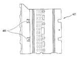
한편, 상기 인버터(370)를 절연시키고, 충격으로부터 보호하는 보호덮개(367)의 전개도는 도5에 도시된 바와 같다.Meanwhile, an exploded view of the
도면을 참조하면, 보호덮개(467)에는 다수개의 홀이 형성되어 있고, 상기 하 부커버에 고정되기 위하여 체결수단이 관통하여 지나가는 제 4체결부(489)들이 형성되어 있다.Referring to the drawings, the
상기 보호덮개(467)에 다수의 홀이 형성된 것은 상기 인버터에서 발생하는 열을 용이하게 외부로 방출하기 위해서이다.The plurality of holes are formed in the
상기 보호덮개(467)은 상기 인버터의 양면을 감싸서 보호하는데, 상기 인버터를 완벽하게 절연시키기 위해서이다. 즉, 인버터 내에 구비된 각종 소자들에서 고전압이 발생하면, 상기 하부커버에 부착되는 인버터의 배면에도 고전압이 인가되어 하부커버를 통해 전류가 흐를 수 있게된다. 따라서, 상기 인버터를 양면으로 패키징함으로써, 상기 인버터로부터 흘러나올 수 있는 전류를 완벽하게 차단한다.The
상기한 바와 같이, 종래에 절연커버 및 금속커버의 기능을 보호덮개(467) 하나로 통합함으로써, 생산비용을 절감하게 되었다.As described above, by integrating the functions of the insulating cover and the metal cover in one
상술한 바와 같이, 본 발명에 따른 액정표시장치는 절연성 및 난연성을 갖는 합성수지로 제작된 보호덮개에 의해 인버터의 양면을 패키징하고, 지지부를 추가적으로 형성함으로써, 인버터로부터 유출되는 전류를 차단하는 절연기능과, 외부의 물리적 충격을 완화하는 보호기능을 통합함에 따라, 작업성이 향상될 수 있고, 생산비용을 절감할 수 있게 되었다.As described above, the liquid crystal display device according to the present invention has an insulation function for packaging the both sides of the inverter by a protective cover made of synthetic resin having insulation and flame retardancy, and additionally forming a support portion to block current flowing out from the inverter. By incorporating protection to mitigate external physical shocks, workability can be improved and production costs can be reduced.
Claims (7)
Translated fromKoreanPriority Applications (1)
| Application Number | Priority Date | Filing Date | Title |
|---|---|---|---|
| KR1020040022446AKR101050868B1 (en) | 2004-03-31 | 2004-03-31 | LCD Display |
Applications Claiming Priority (1)
| Application Number | Priority Date | Filing Date | Title |
|---|---|---|---|
| KR1020040022446AKR101050868B1 (en) | 2004-03-31 | 2004-03-31 | LCD Display |
Publications (2)
| Publication Number | Publication Date |
|---|---|
| KR20050096774A KR20050096774A (en) | 2005-10-06 |
| KR101050868B1true KR101050868B1 (en) | 2011-07-20 |
Family
ID=37276786
Family Applications (1)
| Application Number | Title | Priority Date | Filing Date |
|---|---|---|---|
| KR1020040022446AExpired - LifetimeKR101050868B1 (en) | 2004-03-31 | 2004-03-31 | LCD Display |
Country Status (1)
| Country | Link |
|---|---|
| KR (1) | KR101050868B1 (en) |
Citations (3)
| Publication number | Priority date | Publication date | Assignee | Title |
|---|---|---|---|---|
| KR20010053088A (en)* | 1998-06-23 | 2001-06-25 | 아메라시아 인터내셔널 테크놀로지, 인크. | Method of making an adhesive preform lid for electronic devices |
| KR20020088196A (en)* | 2001-05-18 | 2002-11-27 | 삼성전자 주식회사 | Liquid crystal display device |
| KR20030020069A (en)* | 2001-08-29 | 2003-03-08 | 주식회사 팬택앤큐리텔 | Apparatus for shielding SAR for a hand mobile telephone |
- 2004
- 2004-03-31KRKR1020040022446Apatent/KR101050868B1/ennot_activeExpired - Lifetime
Patent Citations (3)
| Publication number | Priority date | Publication date | Assignee | Title |
|---|---|---|---|---|
| KR20010053088A (en)* | 1998-06-23 | 2001-06-25 | 아메라시아 인터내셔널 테크놀로지, 인크. | Method of making an adhesive preform lid for electronic devices |
| KR20020088196A (en)* | 2001-05-18 | 2002-11-27 | 삼성전자 주식회사 | Liquid crystal display device |
| KR20030020069A (en)* | 2001-08-29 | 2003-03-08 | 주식회사 팬택앤큐리텔 | Apparatus for shielding SAR for a hand mobile telephone |
Also Published As
| Publication number | Publication date |
|---|---|
| KR20050096774A (en) | 2005-10-06 |
Similar Documents
| Publication | Publication Date | Title |
|---|---|---|
| KR101035502B1 (en) | LCD module using light emitting diode | |
| KR101255833B1 (en) | Liquid crystal display device | |
| KR102113610B1 (en) | Borderless-type liquid crystal display device and method for assembling the same | |
| US8264635B2 (en) | Liquid crystal display having a top case with first and second frame members that are physically separated | |
| KR20100078296A (en) | Liquid crystal display device module | |
| US20050264714A1 (en) | Liquid crystal display device | |
| KR100710168B1 (en) | Liquid crystal display | |
| KR20050039021A (en) | Liquid crystal display device module | |
| US20070035689A1 (en) | Printed circuit board and liquid crystal display having the same | |
| US10451920B2 (en) | Display device and method of manufacturing the same | |
| KR101255279B1 (en) | Backlight Unit | |
| KR101287206B1 (en) | Liquid Crystal Display Module | |
| KR101050868B1 (en) | LCD Display | |
| KR20130011175A (en) | Liquid crystal display | |
| KR101213406B1 (en) | Liquid crystal display device module | |
| KR101513159B1 (en) | Structure for jointing liquid crystal display device | |
| KR100962644B1 (en) | LCD Display | |
| KR101753910B1 (en) | Liquid crystal display device | |
| KR100544817B1 (en) | LCD Module | |
| KR101010508B1 (en) | LCD Display | |
| KR20080000848A (en) | Liquid crystal display module | |
| KR100959128B1 (en) | LCD Display | |
| KR101175563B1 (en) | Structure of assembling liquid crystal display | |
| KR20070005806A (en) | Backlight Assembly and Liquid Crystal Display Using Same | |
| KR20080010930A (en) | Display |
Legal Events
| Date | Code | Title | Description |
|---|---|---|---|
| PA0109 | Patent application | Patent event code:PA01091R01D Comment text:Patent Application Patent event date:20040331 | |
| PG1501 | Laying open of application | ||
| A201 | Request for examination | ||
| PA0201 | Request for examination | Patent event code:PA02012R01D Patent event date:20090218 Comment text:Request for Examination of Application Patent event code:PA02011R01I Patent event date:20040331 Comment text:Patent Application | |
| E902 | Notification of reason for refusal | ||
| PE0902 | Notice of grounds for rejection | Comment text:Notification of reason for refusal Patent event date:20100729 Patent event code:PE09021S01D | |
| E90F | Notification of reason for final refusal | ||
| PE0902 | Notice of grounds for rejection | Comment text:Final Notice of Reason for Refusal Patent event date:20101227 Patent event code:PE09021S02D | |
| E701 | Decision to grant or registration of patent right | ||
| PE0701 | Decision of registration | Patent event code:PE07011S01D Comment text:Decision to Grant Registration Patent event date:20110628 | |
| GRNT | Written decision to grant | ||
| PR0701 | Registration of establishment | Comment text:Registration of Establishment Patent event date:20110714 Patent event code:PR07011E01D | |
| PR1002 | Payment of registration fee | Payment date:20110714 End annual number:3 Start annual number:1 | |
| PG1601 | Publication of registration | ||
| FPAY | Annual fee payment | Payment date:20140630 Year of fee payment:4 | |
| PR1001 | Payment of annual fee | Payment date:20140630 Start annual number:4 End annual number:4 | |
| FPAY | Annual fee payment | Payment date:20150629 Year of fee payment:5 | |
| PR1001 | Payment of annual fee | Payment date:20150629 Start annual number:5 End annual number:5 | |
| FPAY | Annual fee payment | Payment date:20160630 Year of fee payment:6 | |
| PR1001 | Payment of annual fee | Payment date:20160630 Start annual number:6 End annual number:6 | |
| FPAY | Annual fee payment | Payment date:20190617 Year of fee payment:9 | |
| PR1001 | Payment of annual fee | Payment date:20190617 Start annual number:9 End annual number:9 | |
| PR1001 | Payment of annual fee | Payment date:20200617 Start annual number:10 End annual number:10 | |
| PR1001 | Payment of annual fee | Payment date:20210614 Start annual number:11 End annual number:11 | |
| PR1001 | Payment of annual fee | Payment date:20220615 Start annual number:12 End annual number:12 | |
| PC1801 | Expiration of term | Termination date:20240930 Termination category:Expiration of duration |