KR101050405B1 - Method of manufacturing semiconductor device having strained channel - Google Patents
Method of manufacturing semiconductor device having strained channelDownload PDFInfo
- Publication number
- KR101050405B1 KR101050405B1KR1020090060876AKR20090060876AKR101050405B1KR 101050405 B1KR101050405 B1KR 101050405B1KR 1020090060876 AKR1020090060876 AKR 1020090060876AKR 20090060876 AKR20090060876 AKR 20090060876AKR 101050405 B1KR101050405 B1KR 101050405B1
- Authority
- KR
- South Korea
- Prior art keywords
- gate spacer
- region
- film
- single crystal
- recess
- Prior art date
- Legal status (The legal status is an assumption and is not a legal conclusion. Google has not performed a legal analysis and makes no representation as to the accuracy of the status listed.)
- Expired - Fee Related
Links
Images


Classifications
- H—ELECTRICITY
- H10—SEMICONDUCTOR DEVICES; ELECTRIC SOLID-STATE DEVICES NOT OTHERWISE PROVIDED FOR
- H10D—INORGANIC ELECTRIC SEMICONDUCTOR DEVICES
- H10D64/00—Electrodes of devices having potential barriers
- H10D64/01—Manufacture or treatment
- H10D64/015—Manufacture or treatment removing at least parts of gate spacers, e.g. disposable spacers
- H—ELECTRICITY
- H10—SEMICONDUCTOR DEVICES; ELECTRIC SOLID-STATE DEVICES NOT OTHERWISE PROVIDED FOR
- H10D—INORGANIC ELECTRIC SEMICONDUCTOR DEVICES
- H10D12/00—Bipolar devices controlled by the field effect, e.g. insulated-gate bipolar transistors [IGBT]
- H10D12/01—Manufacture or treatment
- H10D12/031—Manufacture or treatment of IGBTs
- H10D12/032—Manufacture or treatment of IGBTs of vertical IGBTs
- H10D12/038—Manufacture or treatment of IGBTs of vertical IGBTs having a recessed gate, e.g. trench-gate IGBTs
- H—ELECTRICITY
- H10—SEMICONDUCTOR DEVICES; ELECTRIC SOLID-STATE DEVICES NOT OTHERWISE PROVIDED FOR
- H10D—INORGANIC ELECTRIC SEMICONDUCTOR DEVICES
- H10D30/00—Field-effect transistors [FET]
- H10D30/60—Insulated-gate field-effect transistors [IGFET]
- H—ELECTRICITY
- H10—SEMICONDUCTOR DEVICES; ELECTRIC SOLID-STATE DEVICES NOT OTHERWISE PROVIDED FOR
- H10D—INORGANIC ELECTRIC SEMICONDUCTOR DEVICES
- H10D30/00—Field-effect transistors [FET]
- H10D30/60—Insulated-gate field-effect transistors [IGFET]
- H10D30/791—Arrangements for exerting mechanical stress on the crystal lattice of the channel regions
- H10D30/797—Arrangements for exerting mechanical stress on the crystal lattice of the channel regions being in source or drain regions, e.g. SiGe source or drain
- H—ELECTRICITY
- H10—SEMICONDUCTOR DEVICES; ELECTRIC SOLID-STATE DEVICES NOT OTHERWISE PROVIDED FOR
- H10D—INORGANIC ELECTRIC SEMICONDUCTOR DEVICES
- H10D62/00—Semiconductor bodies, or regions thereof, of devices having potential barriers
- H10D62/01—Manufacture or treatment
- H10D62/021—Forming source or drain recesses by etching e.g. recessing by etching and then refilling
- H—ELECTRICITY
- H10—SEMICONDUCTOR DEVICES; ELECTRIC SOLID-STATE DEVICES NOT OTHERWISE PROVIDED FOR
- H10D—INORGANIC ELECTRIC SEMICONDUCTOR DEVICES
- H10D62/00—Semiconductor bodies, or regions thereof, of devices having potential barriers
- H10D62/80—Semiconductor bodies, or regions thereof, of devices having potential barriers characterised by the materials
- H10D62/82—Heterojunctions
- H10D62/822—Heterojunctions comprising only Group IV materials heterojunctions, e.g. Si/Ge heterojunctions
Landscapes
- Insulated Gate Type Field-Effect Transistor (AREA)
Abstract
Translated fromKoreanDescription
Translated fromKorean본 발명은 반도체장치 제조 방법에 관한 것으로서, 특히 스트레인드채널(Strained channel)을 갖는 반도체장치 제조 방법에 관한 것이다.BACKGROUND OF THE INVENTION 1. Field of the Invention The present invention relates to a method of manufacturing a semiconductor device, and more particularly, to a method of manufacturing a semiconductor device having a strained channel.
반도체 장치의 고직접화가 계속되면서 MOS 소자의 게이트절연막 두께 및 채널 길이도 계속 감소하고 있다. 게이트 절연막의 두께 감소 및 채널 길이의 감소는 캐리어인 전자 또는 정공의 이동도(mobility)를 증가시켜 소자의 속도 및 동작 전류가 증가한다.As the semiconductor devices become more directly connected, the gate insulating film thickness and the channel length of the MOS devices continue to decrease. The decrease in the thickness of the gate insulating layer and the decrease in the channel length increase the mobility of electrons or holes serving as carriers, thereby increasing the speed and operating current of the device.
그러나, 채널 길이의 감소는 짧은 채널 효과(short channel effect)를 일으키는 문제가 있으며, 게이트 절연막의 두께 감소는 게이트 누설 전류를 증가시킨다. 짧은 채널 효과를 개선하기 위해서는 채널 도핑을 증가시키게 되는데 이것은 캐리어의 이동을 방해하여 채널 길이의 감소에도 불구하고 캐리어 이동도의 개선이 저하되게 된다.However, the reduction of the channel length has a problem of causing a short channel effect, and the reduction of the thickness of the gate insulating film increases the gate leakage current. In order to improve the short channel effect, channel doping is increased, which hinders the movement of the carrier, thereby reducing the improvement of the carrier mobility despite the decrease in the channel length.
소자의 동작 속도 및 동작 전류를 개선하기 위해 채널에 스트레인을 유발하여 캐리어 이동도(mobility)를 증가시키려는 여러가지 방법이 제안되었다. 특히 게이트 측벽 근처의 소스/드레인 영역을 리세스(recess) 식각한 후 실리콘기판과 격자상수가 다른 4족 원소의 에피택셜 박막을 선택적으로 증착하여 채널에 스트레스(stress)를 인가하여 스트레인드채널(strained channel)을 형성하는 방법이 많이 연구되고 있다.Several methods have been proposed to increase carrier mobility by inducing strain in the channel to improve the device's operating speed and operating current. In particular, after the recess / etching of the source / drain region near the gate sidewall, the epitaxial thin film of the Group 4 element having a different lattice constant from the silicon substrate is selectively deposited to apply a stress to the channel to strain the channel. Many methods for forming strained channels have been studied.
위와 같은 리세스된 소스/드레인 영역에 선택적 에피택셜 실리콘-저마늄(SiGe), 또는 실리콘-카본(SiC)을 채워서 스트레인드 채널을 만드는 종래기술을 도면과 함께 설명하면 다음과 같다.The prior art of filling strained source / drain regions with selective epitaxial silicon-germanium (SiGe) or silicon-carbon (SiC) to form a strained channel will now be described with reference to the accompanying drawings.
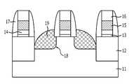
도 1a 내지 도 1d는 종래기술에 따른 스트레인드채널을 갖는 반도체장치의 제조 방법을 도시한 도면이다.1A to 1D illustrate a method of manufacturing a semiconductor device having a strained channel according to the prior art.
도 1a에 도시된 바와 같이, 실리콘기판(11)에 소자간 절연을 위한 필드산화막(12)을 형성한 후, 게이트절연막(13), 게이트폴리실리콘막(14), 게이트금속막(15) 및 게이트하드마스크막(16)으로 이루어진 게이트패턴을 형성한다.As shown in FIG. 1A, after the
이어서, 게이트패턴의 측벽에 게이트스페이서(17)를 형성한 후, 소스 영역 및 드레인 영역으로 예정된 영역을 소정 깊이로 리세스(recess) 시켜 리세스영역(18)을 형성한다.Subsequently, after the
도 1b에 도시된 바와 같이, 선택적에피택셜성장(SEG) 공정에 의해 리세스 영역(18)에 단결정막(19)을 형성한다. 단결정막(19)은 실리콘기판과 격자 상수가 다른 실리콘저마늄(SiGe), 실리콘카본(SiC) 또는 실리콘저마늄카본(SiGeC) 등을 포함 한다.As shown in FIG. 1B, the
위와 같은 단결정막(19)에 의해 유발되는 채널 스트레인의 크기는 저마늄(또는 카본)의 농도 증가, 게이트 스페이서 하부 측면 깊이(Lateral Depth)의 증가 및 하부 리세스(recess depth)의 증가에 따라 커진다.The magnitude of the channel strain caused by the
그러나, 장치의 고집적화에 따라 채널 길이가 짧아지는 경우, 리세스를 깊게 하고 인시츄로 도핑하는 경우 접합깊이(Junction Depth)가 크므로 짧은 채널 효과에 의한 장치의 특성 악화 현상이 나타나게 된다. 다시 말하면, 스트레인드 채널 효과를 위해서는 리세스 깊이가 깊어야 하지만 그 깊이가 깊을수록 짧은 채널 효과가 악화되어 깊게 할 수 없는 기술적 모순에 봉착하게 된다.However, when the channel length becomes short due to the high integration of the device, the depth of the recess and the doping in-situ increase the junction depth, resulting in deterioration of the device characteristics due to the short channel effect. In other words, the depth of the recess must be deep for the strained channel effect, but the deeper the depth, the shorter the channel effect is exacerbated and the technical contradiction cannot be deepened.
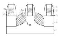
이를 개선하기 위한 방법으로서, 도 1c 및 도 1d와 같이 언도우프드(un-doped)로 단결정막(20)을 먼저 증착한 후 후속에 이온 주입(도 1c의 화살표 참조))을 실시하여 불순물이 도핑된 단결정막(21A)을 형성하고 있다. 다른 방법으로서, 도시되지는 않았지만 언도우프드로 단결정막을 일부 증착을 하고 나머지 일부만 인시츄 도핑으로 스택(stack)을 쌓는 방법등이 사용되고 있으나, 이 방법들도 다음과 같은 문제점이 있다.As a method for improving this, as shown in FIGS. 1C and 1D, the
먼저 언도우프드로 증착을 하고 후속의 이온 주입을 실시하는 방법에서는 필드산화막 근처에서 나타나는 패싯(facet)에 의해 이온주입 깊이 및 프로파일의 조절이 어렵다. 즉 도 1c와 같이 언도우프드로 증착한 단결정막의 필드산화막 근처 패싯에 의해 도 1d와 같이 깊이 조절이 안된 도핑 프로파일이 나타나며, 이에 따라 짧은 채널 효과에 의한 장치의 특성 악화가 나타나며, 접합 누설 전류(Junction Leakage)가 증가하는 문제점이 있다.In the method of first depositing with undoped and subsequent ion implantation, it is difficult to control ion implantation depth and profile by facets appearing near the field oxide film. That is, as shown in FIG. 1C, a doping profile without depth control is shown by the facet near the field oxide layer of the undoped single crystal film as shown in FIG. 1C, resulting in deterioration of device characteristics due to a short channel effect, and a junction leakage current (Junction). Leakage) has a problem that increases.
언도우프드로 일부 증착하고, 필요로 하는 접합깊이 만큼만 인시츄 도핑된 단결정막을 증착하는 방법은 일부 개선의 효과는 있지만 여전히 패싯이 존재하는 상태이므로 도핑 프로파일의 조절이 어려운 부분은 완전히 개선되지 않는다. 특히 데이타 저장용 DRAM의 경우, 집적도의 증가에 따라 주변회로(Periperal)에 트랜지스터의 갯수가 급격히 증가하므로, 게이트패턴과 필드산화막간 거리가 가까워서, 즉 패싯 위치와 채널간 거리가 가까워서 패싯(facet)에 의한 영향이 커짐에 따라 이 방법에 의한 개선도 거의 실현되기 어렵다.The method of depositing partially undoped and depositing an in-situ doped single-crystal film only to the required junction depth has some improvement, but still has facets, so the difficult control of the doping profile is not completely improved. In particular, in the case of DRAM for data storage, the number of transistors in the peripheral circuit increases rapidly as the integration density increases, so that the distance between the gate pattern and the field oxide film is close, that is, the facet position and the channel distance are close to facet. As the influence is increased, the improvement by this method is hardly realized.
본 발명은 상기한 종래기술에 따른 문제점을 해결하기 위해 제안된 것으로서, 스트레인드 채널 효과를 극대화하면서도 짧은 채널 효과를 억제할 수 있는 반도체장치 제조 방법을 제공하는데 그 목적이 있다.SUMMARY OF THE INVENTION The present invention has been proposed to solve the problems according to the prior art, and an object thereof is to provide a method of manufacturing a semiconductor device capable of maximizing a strained channel effect and suppressing a short channel effect.
또한, 본 발명의 다른 목적은 스트레인드 채널을 위한 리세스영역에 단결정막을 성장시킬 때 필드산화막 근처에서 패싯이 발생되는 것을 방지할 수 있는 반도체장치 제조 방법을 제공하는데 있다.Another object of the present invention is to provide a method of manufacturing a semiconductor device capable of preventing facets from being generated near a field oxide film when growing a single crystal film in a recessed region for a strain channel.
상기 목적을 달성하기 위한 본 발명의 반도체장치 제조 방법은 실리콘기판 상에 게이트패턴을 형성하는 단계; 상기 게이트패턴의 양측벽에 게이트스페이서를 형성하는 단계; 상기 게이트스페이서 측벽에 더미게이트스페이서를 형성하는 단계; 상기 실리콘기판을 리세스식각하여 상기 게이트패턴 아래의 채널영역 방향으로 측면이 확장된 리세스영역을 형성하는 단계; 에피택셜 성장을 통해 소스영역 및 드레인영역이 되는 단결정막을 상기 리세스영역에 채우는 단계; 및 상기 더미게이트스페이서를 제거하는 단계를 포함하는 것을 특징으로 한다.A semiconductor device manufacturing method of the present invention for achieving the above object comprises the steps of forming a gate pattern on a silicon substrate; Forming gate spacers on both sidewalls of the gate pattern; Forming a dummy gate spacer on sidewalls of the gate spacer; Recessing the silicon substrate to form a recess region having a side surface extending in a direction of a channel region under the gate pattern; Filling the recess region with a single crystal film serving as a source region and a drain region through epitaxial growth; And removing the dummy gate spacer.
또한, 본 발명의 반도체장치 제조 방법은 필드산화막이 형성된 실리콘기판 상에 게이트패턴을 형성하는 단계; 상기 게이트패턴의 양측벽에 게이트스페이서를 형성하는 단계; 상기 게이트스페이서 측벽에 더미게이트스페이서를 형성하는 단계; 상기 더미게이트스페이서와 필드산화막 사이의 실리콘기판을 리세스식각하여 양쪽 측면이 기울기 프로파일을 갖는 리세스영역을 형성하는 단계; 에피택셜 성장을 통해 소스영역 및 드레인영역이 되는 단결정막을 상기 리세스영역에 채우는 단계; 및 상기 더미게이트스페이서를 제거하는 단계를 포함하는 것을 특징으로 한다.In addition, the semiconductor device manufacturing method of the present invention comprises the steps of forming a gate pattern on a silicon substrate on which a field oxide film is formed; Forming gate spacers on both sidewalls of the gate pattern; Forming a dummy gate spacer on sidewalls of the gate spacer; Recessing the silicon substrate between the dummy gate spacer and the field oxide layer to form a recess region having a slope profile at both sides thereof; Filling the recess region with a single crystal film serving as a source region and a drain region through epitaxial growth; And removing the dummy gate spacer.
상술한 본 발명은 더미게이트스페이서를 이용하여 리세스영역의 식각프로파일을 조절하므로써 채널 근접에 의한 스트레인 효과를 극대화하면서도 깊이 증가에 의해 발생하는 짧은 채널 효과를 억제할 수 있는 효과가 있다.The present invention described above has the effect of suppressing the short channel effect caused by the depth increase while maximizing the strain effect due to channel proximity by adjusting the etch profile of the recess region using the dummy gate spacer.
또한, 본 발명은 리세스영역의 식각프로파일을 조절하므로써 필드산화막 근처에서의 패싯을 방지할 수 있고, 더미 게이트 스페이서를 제거한 후 드러나는 단결정막의 표면은 종래기술보다 표면적이 증가하게 되어 면저항의 감소에 기여할 수 있다.In addition, the present invention can prevent the facet near the field oxide film by adjusting the etch profile of the recess region, and the surface of the single crystal film exposed after removing the dummy gate spacer increases the surface area than the prior art, thereby contributing to the reduction of the sheet resistance. Can be.
또한, 종래기술과 달리 박막 증착 장비에서 증착 직전에 인시츄(in-situ)로 리세스(recess) 식각을 실시하므로써 실리콘기판과 단결정막간의 계면을 깨끗하게 유지할 수 있다. 이에 따라 품질이 우수한 단결정막을 얻을 수 있으므로 접합 누설 전류(Junction Leakage Current)가 개선된 장치 특성을 얻는데 기여할 수 있다.In addition, unlike the prior art, by performing a recess etching in-situ immediately before deposition in a thin film deposition apparatus, the interface between the silicon substrate and the single crystal film can be kept clean. As a result, a single crystal film having excellent quality can be obtained, and thus, junction leakage current can contribute to obtaining improved device characteristics.
이하 본 발명이 속하는 기술분야에서 통상의 지식을 가진자가 본 발명의 기 술적 사상을 용이하게 실시할 수 있을 정도로 상세히 설명하기 위하여, 본 발명의 가장 바람직한 실시예를 첨부도면을 참조하여 설명하기로 한다.DETAILED DESCRIPTION Hereinafter, the most preferred embodiments of the present invention will be described with reference to the accompanying drawings so that those skilled in the art can easily implement the technical idea of the present invention. .
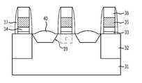
도 2a 내지 도 2e는 본 발명의 실시예에 따른 반도체장치의 스트레인드 채널 형성 방법을 도시한 도면이다.2A through 2E are diagrams illustrating a strain channel forming method of a semiconductor device in accordance with an embodiment of the present invention.
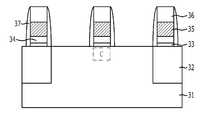
도 2a에 도시된 바와 같이, 실리콘기판(31)에 소자간 절연을 위한 필드산화막(32)을 형성한다. 여기서, 필드산화막(32)은 STI 공정을 이용하여 형성할 수 있고, 필드산화막에 의해 활성영역이 정의된다.As shown in FIG. 2A, a
이어서, 게이트절연막(33), 게이트폴리실리콘막(34), 게이트금속막(35) 및 게이트하드마스크막(36)으로 이루어진 게이트 패턴을 형성한다. 게이트패턴 아래에는 채널영역(C)이 형성된다.Subsequently, a gate pattern including the
이어서, 게이트패턴의 양측벽에 접하는 게이트스페이서(37)를 형성한다. 여기서, 게이트트스페이서(37)은 스페이서절연막을 증착한 후 에치백하여 형성할 수 있다. 게이트스페이서(37)로 사용되는 스페이서절연막은 질화막 또는 산화막을 단독으로 사용하거나 또는, 질화막과 산화막을 적층하여 사용할 수 있다.Subsequently,
도 2b에 도시된 바와 같이, 게이트스페이서(37)의 측벽에 더미 게이트스페이서(38)를 형성한다. 더미 게이트스페이서(38)는 후속 공정에서 제거가 가능한 물질로 형성한다. 예를 들어, 더미 게이트 스페이서(38)는 산화막 또는 산화막과 질화막의 적층막으로 구성될 수 있으나, 바람직하게는 산화막으로 형성된다. 더미 게이트트스페이서(38)은 산화막을 증착한 후 에치백하여 형성할 수 있다.As shown in FIG. 2B, a
이와 같이, 더미 게이트스페이서(38)를 형성하면, 더미게이트스페이서(38)의 폭만큼 채널영역으로부터의 거리가 더 멀어진다.As such, when the
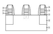
도 2c에 도시된 바와 같이, 실리콘기판(31)을 선택적에피택셜성장 공정이 이루어질 박막 증착 장비에 장착한다.As shown in FIG. 2C, the
이어서, 박막 증착 장비에서 식각 가스를 사용하여 더미 게이트 스페이서(38)의 하부 및 실리콘기판(31) 아래로 적절한 깊이가 리세스되도록 등방성 식각을 이용한 리세스 식각을 실시한다. 이때, 박막 증착 장비에 장착하기 전에 습식방법 또는 건식방법을 이용하거나, 또는 습식과 건식을 모두 사용하여 인시츄 세정 공정을 진행할 수 있다. 이러한 인시츄 세정 공정에 의해 자연산화막 및 기타 표면 물질을 모두 제거하여 깨끗한 실리콘기판 표면을 드러나게 하는 것이 중요하다. 세정공정시 게이트스페이서(37) 및 더미 게이트 스페이서(38)의 손실을 최소화할 수 있는 선택비가 좋은 가스 또는 용액을 사용한다. 세정공정은 상온부터 600℃ 이하의 낮은 온도 범위에서 진행한다.Subsequently, recess etching using isotropic etching is performed so that an appropriate depth is recessed under the
위와 같은 등방성 식각에 의해 일정 깊이의 리세스영역(39)이 형성되며, 리세스영역은 양쪽 측벽은 기울기를 갖고, 바닥면은 평탄할 수 있다. 부연 설명하면, 리세스영역(39)은 게이트스페이서(37) 하부에서는 채널영역(C)에 가깝고 깊이가 깊어질수록 채널영역(C)과 멀어지는 기울기(Slope)의 식각 프로파일을 갖는다.By the isotropic etching as described above, a recessed
리세스 식각을 위한 식각 가스는 염화수소(HCl), 염소(Cl2) 등의 실리콘기판을 등방성으로 식각이 가능한 가스를 사용한다.As the etching gas for the recess etching, a gas capable of isotropically etching silicon substrates such as hydrogen chloride (HCl) and chlorine (Cl2 ) is used.
리세스 식각은 후속 증착과 진공 상태가 깨지지 않는 상황에서 별도의 챔버 를 사용할 수 있고, 또한 리세스 식각은 후속 증착과 진공 상태가 깨지지 않는 상태에서 별도의 등방성 습식 용액을 사용할 수 있다.The recess etching may use a separate chamber in a situation where the subsequent deposition and vacuum are not broken, and the recess etching may also use a separate isotropic wet solution in the condition where the subsequent deposition and vacuum are not broken.
리세스 식각의 깊이는 얻고자 하는 소자 특성에 필요한 채널에 인가될 스트레스(stress)의 양에 따라 결정된다. 바람직하게는 100∼1000Å의 깊이이다.The depth of the recess etch is determined by the amount of stress to be applied to the channel required for the device characteristics to be obtained. Preferably it is 100-1000 micrometers in depth.
리세스 식각의 옆면 식각 거리는 게이트 스페이서(37)의 두께, 채널 길이, 게이트패턴의 높이등을 고려하여 최대한 깊게 들어가도록 조절한다.The side etch distance of the recess etch is adjusted to be as deep as possible in consideration of the thickness of the
리세스 식각은 게이트 스페이서(37) 또는 더미 게이트 스페이서(38)의 하부에 위치하도록 소자 특성에 따라 조절 가능하며, 필드산화막(32) 측면에서는 실리콘기판의 일부가 잔류하도록 조절한다.The recess etching may be adjusted according to the device characteristics so as to be positioned under the
리세스 식각이 완료되면, 도 2d에 도시된 바와 같이, 연속적으로 선택적 에피택셜 성장 공정을 진행하여 리세스 영역(39)에 소스영역 및 드레인영역이 되는 단결정막(40)을 성장시킨다. 단결정막(40)은 실리콘 기판(31)과 격자 상수가 다른 실리콘저마늄(SiGe), 실리콘카본(SiC), 실리콘저마늄카본(SiGeC) 등의 단일막, 실리콘막/실리콘저마늄막(또는 실리콘-카본)/실리콘막의 스택(stack)일 수 있다. PMOS 장치인 경우는 캐리어인 홀(hole)의 이동도를 높이기 위해 실리콘 기판보다 격자상수가 커서 압축 스트레스(compressive stress)를 유발하는 인시츄 붕소(Boron) 도핑된 에피택셜 실리콘저마늄막(또는 실리콘막/실리콘저마늄막의 스택)을 사용하며, NMOS 장치의 경우는 캐리어인 전자(electron)의 이동도를 높이기 위해 실리콘 기판보다 격자 상수가 작아서 인장 스트레스(tensile stress)를 유발하는 인시츄로 인(P) 또는 비소(As)가 도핑된 에피택셜 실리콘카본막 (또는 실리콘막 /실리콘카본막의 스택)을 사용한다.When the recess etching is completed, as shown in FIG. 2D, a selective epitaxial growth process is continuously performed to grow the
단결정막(40)은 LPCVD(Low Pressure CVD), VLPCVD(Very Low Pressure CVD), PE-CVD(Plasma Enhanced-CVD), UHVCVD(Ultrahigh Vacuum CVD), RTCVD(Rapid Thermal CVD), APCVD(Atmosphere Pressure CVD), MBE(Molecular Beam Epitaxy) 등의 장비에서 형성된다.The
단결정막(40)의 증착 온도는 400∼800℃ 범위이다.The deposition temperature of the
위와 같이 선택적에피택셜성장을 통해 성장되는 단결정막(40)은 패싯(facet)이 형성되지 않아 인시츄(in-situ)의 방법으로 도핑을 하거나, 또는 도핑을 하지 않고 후속 이온주입으로 도펀트(dopant) 프로파일을 조절하는 것이 가능하다.As described above, the
단결정막(40)은 더미 게이트 스페이서(38)의 하단부보다 높게 형성되어 후속 더미 게이트 스페이서의 제거후 표면적이 증가하여 면저항 감소가 가능하다.Since the
위와 같은 단결정막(40)에 의해 유발되는 채널 스트레인의 크기는 저마늄(또는 카본)의 농도 증가, 게이트 스페이서 하부 측면 깊이(Lateral Depth)의 증가 및 하부 리세스(recess depth)의 증가에 따라 커진다. 저마늄 및 카본 농도는 장치 특성에 따라 결정되며, 바람직하게는 저마늄의 경우 5%∼50%, 카본의 경우 0.1%∼10% 범위이다.The magnitude of the channel strain caused by the
단결정막(40)은 더미(dummy) 게이트 스페이서의 하단부 이상의 두께로 증착되어, 후속 공정에서 더미 게이트 스페이서를 제거했을때 약간 높게 형성되도록 한다. 단결정막의 두께는 리세스 깊이 및 소자 특성에 따라 결정되는 것으로, 바람직하게는 100∼2000Å의 범위이다.The
또한, 단결정막(40)은 인시츄로 도핑을 하거나, 도핑을 하지 않고 후속에서 이온주입에 의해 도핑을 할 수도 있다. 이온 주입의 경우 더미(dummy) 게이트 스페이서 제거 전, 또는 제거후에 하는 것을 선택함으로서 장치의 특성 조절이 가능하다.In addition, the
상술한 도 2c 및 도 2d에 도시된 것처럼, 리세스식각 및 단결정막 증착이 연속으로 실시됨에 따라 실리콘 기판(31)과 단결정막(40)간 계면 결함이 억제되며, 단결정막(40)의 결함도 억제된다.As shown in FIGS. 2C and 2D, the interface defect between the
도 2e에 도시된 바와 같이, 더미 게이트 스페이서(38)를 제거한 후, 후속의 장치 제조 공정을 실시하여 스트레인드 채널을 갖는 장치를 완성한다.As shown in FIG. 2E, after removing the
더미 게이트 스페이서(38)는 단결정막(40) 증착 후 바로 제거하거나 또는 더미 게이트 스페이서(38)를 이용하여 채널영역(C)에 대한 영향을 줄이면서 추가의 이온 주입등으로 저항을 감소시키는 것이 가능하다.The
후속하여 실리사이드를 더 형성할 수 있다. 티타늄 실리사이드(TiSi2), 코발트 실리사이드(CoSi2), 니켈 실리사이드(NiSi) 등을 사용하여 소스 영역 및 드레인 영역의 면저항을 감소시킬 수 있다.Subsequently, silicide may be further formed. Titanium silicide (TiSi2 ), cobalt silicide (CoSi2 ), nickel silicide (NiSi) and the like may be used to reduce the sheet resistance of the source and drain regions.
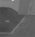
도 3은 본 발명의 실시예에 따른 단결정막 성장후의 상태를 촬영한 사진으로서, 필드산화막 근처에서 패싯없이 단결정막(SiGe)이 성장되고 있음을 알 수 있다. 아울러, 필드산화막 근처에서 일정량의 실리콘기판을 잔류시키면서 기울기를 갖고 리세스영역이 형성되고 있음을 알 수 있다.3 is a photograph showing a state after the growth of the single crystal film according to the embodiment of the present invention, and it can be seen that the single crystal film (SiGe) is grown without facets near the field oxide film. In addition, it can be seen that the recess region is formed with a slope while leaving a certain amount of the silicon substrate near the field oxide film.
상술한 본 발명에서는 후속 공정에서 제거될 수 있는 물질을 사용한 더미(dummy) 게이트 스페이서를 구비한 상태에서 박막 증착 장비에서의 식각 가스로 인시츄(In-situ) 리세스(recess) 식각을 진행함으로써 게이트 스페이서에 가까운 하부에서는 채널에 가깝게 형성되고, 리세스영역의 깊이가 깊어질수록 채널에서 멀게 형성되도록 프로파일을 조절하여 스트레인채널 효과를 극대화하면서도 짧은 채널 효과를 억제한다. 또한 필드산화막 근처의 패싯(facet)을 방지하며, 더미 게이트 스페이서를 제거한 후 드러나는 단결정막 표면의 표면적 증가로 면저항의 감소에 기여할 수 있고, 인시츄 리세스 식각 방법에 의해 품질이 우수한 단결정막을 얻을 수 있다.In the present invention described above, by performing in-situ recess etching with an etching gas in a thin film deposition apparatus with a dummy gate spacer using a material that can be removed in a subsequent process. The lower portion close to the gate spacer is formed closer to the channel, and as the depth of the recess region increases, the profile is adjusted to be formed farther from the channel to maximize the strain channel effect while suppressing the short channel effect. In addition, it prevents facets near the field oxide film, and contributes to reduction of sheet resistance by increasing the surface area of the surface of the single crystal film that is exposed after removing the dummy gate spacer, and obtains a high quality single crystal film by an in situ recess etching method. have.
본 발명에서는 게이트 스페이서 형성 후, 별도의 식각 장비에서 리세스 식각을 하던 방식과 달리, 게이트 스페이서 위에 후속 공정에서 제거될 수 있는 더미 게이트 스페이서를 추가로 형성한 상태에서 박막 증착 장비에서 염화수소(HCl), 염소(Cl2)와 같은 식각 가스를 사용하여 인시츄(In-situ)로 등방성의 리세스(recess) 식각을 실시한다. 하여 게이트 스페이서의 가까운 하부에서는 채널에 가깝게 형성되고, 깊어질수록 멀게 형성되도록 식각 프로파일을 조절하여, 채널에의 근접에 의해 스트레인 효과를 극대화하면서도 깊이 증가에 의해 발생하는 짧은 채널 효과를 억제할 수 있다.In the present invention, unlike the method of recess etching in a separate etching equipment after the formation of the gate spacer, hydrogen chloride (HCl) in the thin film deposition equipment with a dummy gate spacer that can be removed in a subsequent process on the gate spacer is further formed , Using an etching gas such as chlorine (Cl 2), isotropic recess etching is performed in-situ. Therefore, the etch profile is formed to be closer to the channel at a lower portion of the gate spacer and to be closer to the channel, so that the short channel effect caused by the depth increase can be suppressed while maximizing the strain effect due to the proximity to the channel. .
또한, 본 발명에 의하면, 더미 스페이서 하부로의 리세스 식각으로 필드산화막 옆면에 실리콘기판의 일부가 잔류하므로 종래 기술에서 문제가 되는 패싯(facet)을 방지할 수 있으며, 더미 게이트 스페이서를 제거한 후 드러나는 선택 적 에피 박막 표면은 기존 기술에서보다 표면적이 증가하게 되어 면저항의 감소에 기여할 수 있다.In addition, according to the present invention, since a part of the silicon substrate remains on the side surface of the field oxide layer due to the recess etching under the dummy spacer, it is possible to prevent a facet, which is a problem in the prior art, and to be exposed after removing the dummy gate spacer. Selective epi thin film surfaces can increase surface area more than in the prior art and contribute to the reduction of sheet resistance.
또한, 종래 기술과 달리 박막 증착 장비에서 증착 직전에 인시츄(in-situ)로 리세스(recess)를 형성하므로 기판과 박막간의 계면을 깨끗하게 유지할 수 있으므로 품질이 우수한 선택적 에피 박막을 얻을 수 있어 누설 전류(Junction Leakage Current)가 개선된 소자 특성을 얻을 수 있다.In addition, unlike in the prior art, in the thin film deposition equipment, a recess is formed in-situ immediately before deposition, so that the interface between the substrate and the thin film can be kept clean, so that an excellent quality epitaxial thin film can be obtained. Device characteristics with improved junction leakage current can be obtained.
또한, 본 발명에서와 같이 리세스 식각과 증착을 일관공정으로 함으로써 공정시간을 단축할 수 있다.In addition, as in the present invention, the process time can be shortened by using the recess etching and the deposition as an integrated process.
본 발명의 기술 사상은 상기 바람직한 실시예에 따라 구체적으로 기술되었으나, 상기 실시예는 그 설명을 위한 것이며, 그 제한을 위한 것이 아님을 주의하여야 한다. 또한, 본 발명의 기술분야의 통상의 전문가라면 본 발명의 기술사상의 범위내의 다양한 실시예가 가능함을 이해할 수 있을 것이다. Although the technical spirit of the present invention has been described in detail according to the above preferred embodiment, it should be noted that the above embodiment is for the purpose of description and not of limitation. In addition, those skilled in the art will appreciate that various embodiments within the scope of the technical idea of the present invention are possible.
도 1a 내지 도 1d는 종래기술에 따른 스트레인드채널을 갖는 반도체장치의 제조 방법을 도시한 도면.1A to 1D illustrate a method of manufacturing a semiconductor device having a strained channel according to the prior art.
도 2a 내지 도 2e는 본 발명의 실시예에 따른 반도체장치의 스트레인드 채널 형성 방법을 도시한 도면.2A to 2E are diagrams illustrating a strain channel forming method of a semiconductor device according to an embodiment of the present invention.
도 3은 본 발명의 실시예에 따른 단결정막 성장후의 상태를 촬영한 사진.Figure 3 is a photograph taken after the growth of a single crystal film according to an embodiment of the present invention.
* 도면의 주요 부분에 대한 부호의 설명* Explanation of symbols for the main parts of the drawings
31 : 실리콘기판 32 : 필드산화막31
37 : 게이트스페이서 38 : 더미게이트스페이서37: gate spacer 38: dummy gate spacer
39 : 리세스영역 40 : 단결정막39: recessed region 40: single crystal film
Claims (18)
Translated fromKoreanPriority Applications (2)
| Application Number | Priority Date | Filing Date | Title |
|---|---|---|---|
| KR1020090060876AKR101050405B1 (en) | 2009-07-03 | 2009-07-03 | Method of manufacturing semiconductor device having strained channel |
| US12/646,207US20110003450A1 (en) | 2009-07-03 | 2009-12-23 | Method for manufacturing semicondutor device with strained channel |
Applications Claiming Priority (1)
| Application Number | Priority Date | Filing Date | Title |
|---|---|---|---|
| KR1020090060876AKR101050405B1 (en) | 2009-07-03 | 2009-07-03 | Method of manufacturing semiconductor device having strained channel |
Publications (2)
| Publication Number | Publication Date |
|---|---|
| KR20110003217A KR20110003217A (en) | 2011-01-11 |
| KR101050405B1true KR101050405B1 (en) | 2011-07-19 |
Family
ID=43412907
Family Applications (1)
| Application Number | Title | Priority Date | Filing Date |
|---|---|---|---|
| KR1020090060876AExpired - Fee RelatedKR101050405B1 (en) | 2009-07-03 | 2009-07-03 | Method of manufacturing semiconductor device having strained channel |
Country Status (2)
| Country | Link |
|---|---|
| US (1) | US20110003450A1 (en) |
| KR (1) | KR101050405B1 (en) |
Families Citing this family (288)
| Publication number | Priority date | Publication date | Assignee | Title |
|---|---|---|---|---|
| US8338884B2 (en) | 2009-05-12 | 2012-12-25 | Taiwan Semiconductor Manufacturing Company, Ltd. | Selective epitaxial growth of semiconductor materials with reduced defects |
| US8492234B2 (en) | 2010-06-29 | 2013-07-23 | International Business Machines Corporation | Field effect transistor device |
| CN102456739A (en)* | 2010-10-28 | 2012-05-16 | 中国科学院微电子研究所 | Semiconductor structure and forming method thereof |
| US20130023129A1 (en) | 2011-07-20 | 2013-01-24 | Asm America, Inc. | Pressure transmitter for a semiconductor processing environment |
| US9847225B2 (en)* | 2011-11-15 | 2017-12-19 | Taiwan Semiconductor Manufacturing Company, Ltd. | Semiconductor device and method of manufacturing the same |
| US9324811B2 (en)* | 2012-09-26 | 2016-04-26 | Asm Ip Holding B.V. | Structures and devices including a tensile-stressed silicon arsenic layer and methods of forming same |
| US10714315B2 (en) | 2012-10-12 | 2020-07-14 | Asm Ip Holdings B.V. | Semiconductor reaction chamber showerhead |
| US20160376700A1 (en) | 2013-02-01 | 2016-12-29 | Asm Ip Holding B.V. | System for treatment of deposition reactor |
| US9129823B2 (en)* | 2013-03-15 | 2015-09-08 | Taiwan Semiconductor Manufacturing Co., Ltd. | Silicon recess ETCH and epitaxial deposit for shallow trench isolation (STI) |
| KR101998666B1 (en) | 2013-06-25 | 2019-10-02 | 삼성전자주식회사 | Semiconductor device and fabricating method thereof |
| US9093298B2 (en)* | 2013-08-22 | 2015-07-28 | Texas Instruments Incorporated | Silicide formation due to improved SiGe faceting |
| US9691898B2 (en)* | 2013-12-19 | 2017-06-27 | Taiwan Semiconductor Manufacturing Co., Ltd. | Germanium profile for channel strain |
| US11015245B2 (en) | 2014-03-19 | 2021-05-25 | Asm Ip Holding B.V. | Gas-phase reactor and system having exhaust plenum and components thereof |
| KR102171023B1 (en)* | 2014-07-21 | 2020-10-29 | 삼성전자주식회사 | Method of fabricating semiconductor devices |
| US10941490B2 (en) | 2014-10-07 | 2021-03-09 | Asm Ip Holding B.V. | Multiple temperature range susceptor, assembly, reactor and system including the susceptor, and methods of using the same |
| US10164050B2 (en) | 2014-12-24 | 2018-12-25 | Taiwan Semiconductor Manufacturing Co., Ltd. | Structure and formation method of semiconductor device structure with gate stack |
| US10276355B2 (en) | 2015-03-12 | 2019-04-30 | Asm Ip Holding B.V. | Multi-zone reactor, system including the reactor, and method of using the same |
| US10458018B2 (en) | 2015-06-26 | 2019-10-29 | Asm Ip Holding B.V. | Structures including metal carbide material, devices including the structures, and methods of forming same |
| KR102302073B1 (en) | 2015-07-28 | 2021-09-14 | 삼성전자주식회사 | A semiconductor device and methods of manufacturing the same |
| US10211308B2 (en) | 2015-10-21 | 2019-02-19 | Asm Ip Holding B.V. | NbMC layers |
| US11139308B2 (en) | 2015-12-29 | 2021-10-05 | Asm Ip Holding B.V. | Atomic layer deposition of III-V compounds to form V-NAND devices |
| US9881821B2 (en) | 2015-12-30 | 2018-01-30 | Taiwan Semiconductor Manufacturing Co., Ltd. | Control wafer making device and method for measuring and monitoring control wafer |
| US10529554B2 (en) | 2016-02-19 | 2020-01-07 | Asm Ip Holding B.V. | Method for forming silicon nitride film selectively on sidewalls or flat surfaces of trenches |
| US10343920B2 (en) | 2016-03-18 | 2019-07-09 | Asm Ip Holding B.V. | Aligned carbon nanotubes |
| US10367080B2 (en) | 2016-05-02 | 2019-07-30 | Asm Ip Holding B.V. | Method of forming a germanium oxynitride film |
| US11453943B2 (en) | 2016-05-25 | 2022-09-27 | Asm Ip Holding B.V. | Method for forming carbon-containing silicon/metal oxide or nitride film by ALD using silicon precursor and hydrocarbon precursor |
| US10612137B2 (en) | 2016-07-08 | 2020-04-07 | Asm Ip Holdings B.V. | Organic reactants for atomic layer deposition |
| US9859151B1 (en) | 2016-07-08 | 2018-01-02 | Asm Ip Holding B.V. | Selective film deposition method to form air gaps |
| US9812320B1 (en) | 2016-07-28 | 2017-11-07 | Asm Ip Holding B.V. | Method and apparatus for filling a gap |
| US9887082B1 (en) | 2016-07-28 | 2018-02-06 | Asm Ip Holding B.V. | Method and apparatus for filling a gap |
| KR102532607B1 (en) | 2016-07-28 | 2023-05-15 | 에이에스엠 아이피 홀딩 비.브이. | Substrate processing apparatus and method of operating the same |
| US11532757B2 (en) | 2016-10-27 | 2022-12-20 | Asm Ip Holding B.V. | Deposition of charge trapping layers |
| US10714350B2 (en) | 2016-11-01 | 2020-07-14 | ASM IP Holdings, B.V. | Methods for forming a transition metal niobium nitride film on a substrate by atomic layer deposition and related semiconductor device structures |
| KR102546317B1 (en) | 2016-11-15 | 2023-06-21 | 에이에스엠 아이피 홀딩 비.브이. | Gas supply unit and substrate processing apparatus including the same |
| KR102762543B1 (en) | 2016-12-14 | 2025-02-05 | 에이에스엠 아이피 홀딩 비.브이. | Substrate processing apparatus |
| US11447861B2 (en) | 2016-12-15 | 2022-09-20 | Asm Ip Holding B.V. | Sequential infiltration synthesis apparatus and a method of forming a patterned structure |
| US11581186B2 (en) | 2016-12-15 | 2023-02-14 | Asm Ip Holding B.V. | Sequential infiltration synthesis apparatus |
| KR102700194B1 (en) | 2016-12-19 | 2024-08-28 | 에이에스엠 아이피 홀딩 비.브이. | Substrate processing apparatus |
| US10269558B2 (en) | 2016-12-22 | 2019-04-23 | Asm Ip Holding B.V. | Method of forming a structure on a substrate |
| US11390950B2 (en) | 2017-01-10 | 2022-07-19 | Asm Ip Holding B.V. | Reactor system and method to reduce residue buildup during a film deposition process |
| US10468261B2 (en) | 2017-02-15 | 2019-11-05 | Asm Ip Holding B.V. | Methods for forming a metallic film on a substrate by cyclical deposition and related semiconductor device structures |
| US10529563B2 (en) | 2017-03-29 | 2020-01-07 | Asm Ip Holdings B.V. | Method for forming doped metal oxide films on a substrate by cyclical deposition and related semiconductor device structures |
| US10770286B2 (en) | 2017-05-08 | 2020-09-08 | Asm Ip Holdings B.V. | Methods for selectively forming a silicon nitride film on a substrate and related semiconductor device structures |
| US12040200B2 (en) | 2017-06-20 | 2024-07-16 | Asm Ip Holding B.V. | Semiconductor processing apparatus and methods for calibrating a semiconductor processing apparatus |
| US11306395B2 (en) | 2017-06-28 | 2022-04-19 | Asm Ip Holding B.V. | Methods for depositing a transition metal nitride film on a substrate by atomic layer deposition and related deposition apparatus |
| KR20190009245A (en) | 2017-07-18 | 2019-01-28 | 에이에스엠 아이피 홀딩 비.브이. | Methods for forming a semiconductor device structure and related semiconductor device structures |
| US11018002B2 (en) | 2017-07-19 | 2021-05-25 | Asm Ip Holding B.V. | Method for selectively depositing a Group IV semiconductor and related semiconductor device structures |
| US10541333B2 (en) | 2017-07-19 | 2020-01-21 | Asm Ip Holding B.V. | Method for depositing a group IV semiconductor and related semiconductor device structures |
| US11374112B2 (en) | 2017-07-19 | 2022-06-28 | Asm Ip Holding B.V. | Method for depositing a group IV semiconductor and related semiconductor device structures |
| US10590535B2 (en) | 2017-07-26 | 2020-03-17 | Asm Ip Holdings B.V. | Chemical treatment, deposition and/or infiltration apparatus and method for using the same |
| TWI815813B (en) | 2017-08-04 | 2023-09-21 | 荷蘭商Asm智慧財產控股公司 | Showerhead assembly for distributing a gas within a reaction chamber |
| US10770336B2 (en) | 2017-08-08 | 2020-09-08 | Asm Ip Holding B.V. | Substrate lift mechanism and reactor including same |
| US10692741B2 (en) | 2017-08-08 | 2020-06-23 | Asm Ip Holdings B.V. | Radiation shield |
| US11139191B2 (en) | 2017-08-09 | 2021-10-05 | Asm Ip Holding B.V. | Storage apparatus for storing cassettes for substrates and processing apparatus equipped therewith |
| US11769682B2 (en) | 2017-08-09 | 2023-09-26 | Asm Ip Holding B.V. | Storage apparatus for storing cassettes for substrates and processing apparatus equipped therewith |
| US11830730B2 (en) | 2017-08-29 | 2023-11-28 | Asm Ip Holding B.V. | Layer forming method and apparatus |
| US11295980B2 (en) | 2017-08-30 | 2022-04-05 | Asm Ip Holding B.V. | Methods for depositing a molybdenum metal film over a dielectric surface of a substrate by a cyclical deposition process and related semiconductor device structures |
| US11056344B2 (en) | 2017-08-30 | 2021-07-06 | Asm Ip Holding B.V. | Layer forming method |
| KR102491945B1 (en) | 2017-08-30 | 2023-01-26 | 에이에스엠 아이피 홀딩 비.브이. | Substrate processing apparatus |
| US10658205B2 (en) | 2017-09-28 | 2020-05-19 | Asm Ip Holdings B.V. | Chemical dispensing apparatus and methods for dispensing a chemical to a reaction chamber |
| US10403504B2 (en) | 2017-10-05 | 2019-09-03 | Asm Ip Holding B.V. | Method for selectively depositing a metallic film on a substrate |
| US10923344B2 (en) | 2017-10-30 | 2021-02-16 | Asm Ip Holding B.V. | Methods for forming a semiconductor structure and related semiconductor structures |
| US11022879B2 (en) | 2017-11-24 | 2021-06-01 | Asm Ip Holding B.V. | Method of forming an enhanced unexposed photoresist layer |
| WO2019103613A1 (en) | 2017-11-27 | 2019-05-31 | Asm Ip Holding B.V. | A storage device for storing wafer cassettes for use with a batch furnace |
| CN111344522B (en) | 2017-11-27 | 2022-04-12 | 阿斯莫Ip控股公司 | Including clean mini-environment device |
| US10872771B2 (en) | 2018-01-16 | 2020-12-22 | Asm Ip Holding B. V. | Method for depositing a material film on a substrate within a reaction chamber by a cyclical deposition process and related device structures |
| TWI799494B (en) | 2018-01-19 | 2023-04-21 | 荷蘭商Asm 智慧財產控股公司 | Deposition method |
| KR102695659B1 (en) | 2018-01-19 | 2024-08-14 | 에이에스엠 아이피 홀딩 비.브이. | Method for depositing a gap filling layer by plasma assisted deposition |
| US11081345B2 (en) | 2018-02-06 | 2021-08-03 | Asm Ip Holding B.V. | Method of post-deposition treatment for silicon oxide film |
| US10896820B2 (en) | 2018-02-14 | 2021-01-19 | Asm Ip Holding B.V. | Method for depositing a ruthenium-containing film on a substrate by a cyclical deposition process |
| WO2019158960A1 (en) | 2018-02-14 | 2019-08-22 | Asm Ip Holding B.V. | A method for depositing a ruthenium-containing film on a substrate by a cyclical deposition process |
| US10731249B2 (en) | 2018-02-15 | 2020-08-04 | Asm Ip Holding B.V. | Method of forming a transition metal containing film on a substrate by a cyclical deposition process, a method for supplying a transition metal halide compound to a reaction chamber, and related vapor deposition apparatus |
| KR102636427B1 (en) | 2018-02-20 | 2024-02-13 | 에이에스엠 아이피 홀딩 비.브이. | Substrate processing method and apparatus |
| US10975470B2 (en) | 2018-02-23 | 2021-04-13 | Asm Ip Holding B.V. | Apparatus for detecting or monitoring for a chemical precursor in a high temperature environment |
| US11473195B2 (en) | 2018-03-01 | 2022-10-18 | Asm Ip Holding B.V. | Semiconductor processing apparatus and a method for processing a substrate |
| US11629406B2 (en) | 2018-03-09 | 2023-04-18 | Asm Ip Holding B.V. | Semiconductor processing apparatus comprising one or more pyrometers for measuring a temperature of a substrate during transfer of the substrate |
| US11114283B2 (en) | 2018-03-16 | 2021-09-07 | Asm Ip Holding B.V. | Reactor, system including the reactor, and methods of manufacturing and using same |
| KR102646467B1 (en) | 2018-03-27 | 2024-03-11 | 에이에스엠 아이피 홀딩 비.브이. | Method of forming an electrode on a substrate and a semiconductor device structure including an electrode |
| US11088002B2 (en) | 2018-03-29 | 2021-08-10 | Asm Ip Holding B.V. | Substrate rack and a substrate processing system and method |
| US11230766B2 (en) | 2018-03-29 | 2022-01-25 | Asm Ip Holding B.V. | Substrate processing apparatus and method |
| KR102600229B1 (en) | 2018-04-09 | 2023-11-10 | 에이에스엠 아이피 홀딩 비.브이. | Substrate supporting device, substrate processing apparatus including the same and substrate processing method |
| US12025484B2 (en) | 2018-05-08 | 2024-07-02 | Asm Ip Holding B.V. | Thin film forming method |
| TWI811348B (en) | 2018-05-08 | 2023-08-11 | 荷蘭商Asm 智慧財產控股公司 | Methods for depositing an oxide film on a substrate by a cyclical deposition process and related device structures |
| US12272527B2 (en) | 2018-05-09 | 2025-04-08 | Asm Ip Holding B.V. | Apparatus for use with hydrogen radicals and method of using same |
| KR102596988B1 (en) | 2018-05-28 | 2023-10-31 | 에이에스엠 아이피 홀딩 비.브이. | Method of processing a substrate and a device manufactured by the same |
| TWI840362B (en) | 2018-06-04 | 2024-05-01 | 荷蘭商Asm Ip私人控股有限公司 | Wafer handling chamber with moisture reduction |
| US11718913B2 (en) | 2018-06-04 | 2023-08-08 | Asm Ip Holding B.V. | Gas distribution system and reactor system including same |
| US11286562B2 (en) | 2018-06-08 | 2022-03-29 | Asm Ip Holding B.V. | Gas-phase chemical reactor and method of using same |
| KR102568797B1 (en) | 2018-06-21 | 2023-08-21 | 에이에스엠 아이피 홀딩 비.브이. | Substrate processing system |
| US10797133B2 (en) | 2018-06-21 | 2020-10-06 | Asm Ip Holding B.V. | Method for depositing a phosphorus doped silicon arsenide film and related semiconductor device structures |
| KR102854019B1 (en) | 2018-06-27 | 2025-09-02 | 에이에스엠 아이피 홀딩 비.브이. | Periodic deposition method for forming a metal-containing material and films and structures comprising the metal-containing material |
| TWI873894B (en) | 2018-06-27 | 2025-02-21 | 荷蘭商Asm Ip私人控股有限公司 | Cyclic deposition methods for forming metal-containing material and films and structures including the metal-containing material |
| US10612136B2 (en) | 2018-06-29 | 2020-04-07 | ASM IP Holding, B.V. | Temperature-controlled flange and reactor system including same |
| US10388513B1 (en) | 2018-07-03 | 2019-08-20 | Asm Ip Holding B.V. | Method for depositing silicon-free carbon-containing film as gap-fill layer by pulse plasma-assisted deposition |
| US10755922B2 (en) | 2018-07-03 | 2020-08-25 | Asm Ip Holding B.V. | Method for depositing silicon-free carbon-containing film as gap-fill layer by pulse plasma-assisted deposition |
| US11309404B2 (en)* | 2018-07-05 | 2022-04-19 | Applied Materials, Inc. | Integrated CMOS source drain formation with advanced control |
| TWI858954B (en)* | 2018-07-05 | 2024-10-11 | 美商應用材料股份有限公司 | Integrated cmos source drain formation with advanced control |
| US11053591B2 (en) | 2018-08-06 | 2021-07-06 | Asm Ip Holding B.V. | Multi-port gas injection system and reactor system including same |
| US11430674B2 (en) | 2018-08-22 | 2022-08-30 | Asm Ip Holding B.V. | Sensor array, apparatus for dispensing a vapor phase reactant to a reaction chamber and related methods |
| US11024523B2 (en) | 2018-09-11 | 2021-06-01 | Asm Ip Holding B.V. | Substrate processing apparatus and method |
| KR102707956B1 (en) | 2018-09-11 | 2024-09-19 | 에이에스엠 아이피 홀딩 비.브이. | Method for deposition of a thin film |
| US11049751B2 (en) | 2018-09-14 | 2021-06-29 | Asm Ip Holding B.V. | Cassette supply system to store and handle cassettes and processing apparatus equipped therewith |
| CN110970344B (en) | 2018-10-01 | 2024-10-25 | Asmip控股有限公司 | Substrate holding apparatus, system comprising the same and method of using the same |
| US11232963B2 (en) | 2018-10-03 | 2022-01-25 | Asm Ip Holding B.V. | Substrate processing apparatus and method |
| KR102592699B1 (en) | 2018-10-08 | 2023-10-23 | 에이에스엠 아이피 홀딩 비.브이. | Substrate support unit and apparatuses for depositing thin film and processing the substrate including the same |
| KR102546322B1 (en) | 2018-10-19 | 2023-06-21 | 에이에스엠 아이피 홀딩 비.브이. | Substrate processing apparatus and substrate processing method |
| KR102605121B1 (en) | 2018-10-19 | 2023-11-23 | 에이에스엠 아이피 홀딩 비.브이. | Substrate processing apparatus and substrate processing method |
| USD948463S1 (en) | 2018-10-24 | 2022-04-12 | Asm Ip Holding B.V. | Susceptor for semiconductor substrate supporting apparatus |
| US12378665B2 (en) | 2018-10-26 | 2025-08-05 | Asm Ip Holding B.V. | High temperature coatings for a preclean and etch apparatus and related methods |
| US11087997B2 (en) | 2018-10-31 | 2021-08-10 | Asm Ip Holding B.V. | Substrate processing apparatus for processing substrates |
| KR102748291B1 (en) | 2018-11-02 | 2024-12-31 | 에이에스엠 아이피 홀딩 비.브이. | Substrate support unit and substrate processing apparatus including the same |
| US11572620B2 (en) | 2018-11-06 | 2023-02-07 | Asm Ip Holding B.V. | Methods for selectively depositing an amorphous silicon film on a substrate |
| US11031242B2 (en) | 2018-11-07 | 2021-06-08 | Asm Ip Holding B.V. | Methods for depositing a boron doped silicon germanium film |
| US10818758B2 (en) | 2018-11-16 | 2020-10-27 | Asm Ip Holding B.V. | Methods for forming a metal silicate film on a substrate in a reaction chamber and related semiconductor device structures |
| US10847366B2 (en) | 2018-11-16 | 2020-11-24 | Asm Ip Holding B.V. | Methods for depositing a transition metal chalcogenide film on a substrate by a cyclical deposition process |
| US12040199B2 (en) | 2018-11-28 | 2024-07-16 | Asm Ip Holding B.V. | Substrate processing apparatus for processing substrates |
| US11217444B2 (en) | 2018-11-30 | 2022-01-04 | Asm Ip Holding B.V. | Method for forming an ultraviolet radiation responsive metal oxide-containing film |
| KR102636428B1 (en) | 2018-12-04 | 2024-02-13 | 에이에스엠 아이피 홀딩 비.브이. | A method for cleaning a substrate processing apparatus |
| US11158513B2 (en) | 2018-12-13 | 2021-10-26 | Asm Ip Holding B.V. | Methods for forming a rhenium-containing film on a substrate by a cyclical deposition process and related semiconductor device structures |
| TWI874340B (en) | 2018-12-14 | 2025-03-01 | 荷蘭商Asm Ip私人控股有限公司 | Method of forming device structure, structure formed by the method and system for performing the method |
| TWI866480B (en) | 2019-01-17 | 2024-12-11 | 荷蘭商Asm Ip 私人控股有限公司 | Methods of forming a transition metal containing film on a substrate by a cyclical deposition process |
| KR102727227B1 (en) | 2019-01-22 | 2024-11-07 | 에이에스엠 아이피 홀딩 비.브이. | Semiconductor processing device |
| CN111524788B (en) | 2019-02-01 | 2023-11-24 | Asm Ip私人控股有限公司 | Method for forming topologically selective films of silicon oxide |
| TWI838458B (en) | 2019-02-20 | 2024-04-11 | 荷蘭商Asm Ip私人控股有限公司 | Apparatus and methods for plug fill deposition in 3-d nand applications |
| TWI873122B (en) | 2019-02-20 | 2025-02-21 | 荷蘭商Asm Ip私人控股有限公司 | Method of filling a recess formed within a surface of a substrate, semiconductor structure formed according to the method, and semiconductor processing apparatus |
| KR102626263B1 (en) | 2019-02-20 | 2024-01-16 | 에이에스엠 아이피 홀딩 비.브이. | Cyclical deposition method including treatment step and apparatus for same |
| TWI845607B (en) | 2019-02-20 | 2024-06-21 | 荷蘭商Asm Ip私人控股有限公司 | Cyclical deposition method and apparatus for filling a recess formed within a substrate surface |
| TWI842826B (en) | 2019-02-22 | 2024-05-21 | 荷蘭商Asm Ip私人控股有限公司 | Substrate processing apparatus and method for processing substrate |
| KR102782593B1 (en) | 2019-03-08 | 2025-03-14 | 에이에스엠 아이피 홀딩 비.브이. | Structure Including SiOC Layer and Method of Forming Same |
| US11742198B2 (en) | 2019-03-08 | 2023-08-29 | Asm Ip Holding B.V. | Structure including SiOCN layer and method of forming same |
| KR102858005B1 (en) | 2019-03-08 | 2025-09-09 | 에이에스엠 아이피 홀딩 비.브이. | Method for Selective Deposition of Silicon Nitride Layer and Structure Including Selectively-Deposited Silicon Nitride Layer |
| JP2020167398A (en) | 2019-03-28 | 2020-10-08 | エーエスエム・アイピー・ホールディング・ベー・フェー | Door openers and substrate processing equipment provided with door openers |
| KR102809999B1 (en) | 2019-04-01 | 2025-05-19 | 에이에스엠 아이피 홀딩 비.브이. | Method of manufacturing semiconductor device |
| KR20200123380A (en) | 2019-04-19 | 2020-10-29 | 에이에스엠 아이피 홀딩 비.브이. | Layer forming method and apparatus |
| KR20200125453A (en) | 2019-04-24 | 2020-11-04 | 에이에스엠 아이피 홀딩 비.브이. | Gas-phase reactor system and method of using same |
| KR20200130121A (en) | 2019-05-07 | 2020-11-18 | 에이에스엠 아이피 홀딩 비.브이. | Chemical source vessel with dip tube |
| US11289326B2 (en) | 2019-05-07 | 2022-03-29 | Asm Ip Holding B.V. | Method for reforming amorphous carbon polymer film |
| KR20200130652A (en) | 2019-05-10 | 2020-11-19 | 에이에스엠 아이피 홀딩 비.브이. | Method of depositing material onto a surface and structure formed according to the method |
| JP7598201B2 (en) | 2019-05-16 | 2024-12-11 | エーエスエム・アイピー・ホールディング・ベー・フェー | Wafer boat handling apparatus, vertical batch furnace and method |
| JP7612342B2 (en) | 2019-05-16 | 2025-01-14 | エーエスエム・アイピー・ホールディング・ベー・フェー | Wafer boat handling apparatus, vertical batch furnace and method |
| USD975665S1 (en) | 2019-05-17 | 2023-01-17 | Asm Ip Holding B.V. | Susceptor shaft |
| USD947913S1 (en) | 2019-05-17 | 2022-04-05 | Asm Ip Holding B.V. | Susceptor shaft |
| USD935572S1 (en) | 2019-05-24 | 2021-11-09 | Asm Ip Holding B.V. | Gas channel plate |
| USD922229S1 (en) | 2019-06-05 | 2021-06-15 | Asm Ip Holding B.V. | Device for controlling a temperature of a gas supply unit |
| KR20200141002A (en) | 2019-06-06 | 2020-12-17 | 에이에스엠 아이피 홀딩 비.브이. | Method of using a gas-phase reactor system including analyzing exhausted gas |
| KR20200141931A (en) | 2019-06-10 | 2020-12-21 | 에이에스엠 아이피 홀딩 비.브이. | Method for cleaning quartz epitaxial chambers |
| KR20200143254A (en) | 2019-06-11 | 2020-12-23 | 에이에스엠 아이피 홀딩 비.브이. | Method of forming an electronic structure using an reforming gas, system for performing the method, and structure formed using the method |
| USD944946S1 (en) | 2019-06-14 | 2022-03-01 | Asm Ip Holding B.V. | Shower plate |
| USD931978S1 (en) | 2019-06-27 | 2021-09-28 | Asm Ip Holding B.V. | Showerhead vacuum transport |
| KR20210005515A (en) | 2019-07-03 | 2021-01-14 | 에이에스엠 아이피 홀딩 비.브이. | Temperature control assembly for substrate processing apparatus and method of using same |
| JP7499079B2 (en) | 2019-07-09 | 2024-06-13 | エーエスエム・アイピー・ホールディング・ベー・フェー | Plasma device using coaxial waveguide and substrate processing method |
| CN112216646A (en) | 2019-07-10 | 2021-01-12 | Asm Ip私人控股有限公司 | Substrate supporting assembly and substrate processing device comprising same |
| KR20210010307A (en) | 2019-07-16 | 2021-01-27 | 에이에스엠 아이피 홀딩 비.브이. | Substrate processing apparatus |
| KR20210010816A (en) | 2019-07-17 | 2021-01-28 | 에이에스엠 아이피 홀딩 비.브이. | Radical assist ignition plasma system and method |
| KR102860110B1 (en) | 2019-07-17 | 2025-09-16 | 에이에스엠 아이피 홀딩 비.브이. | Methods of forming silicon germanium structures |
| US11643724B2 (en) | 2019-07-18 | 2023-05-09 | Asm Ip Holding B.V. | Method of forming structures using a neutral beam |
| KR20210010817A (en) | 2019-07-19 | 2021-01-28 | 에이에스엠 아이피 홀딩 비.브이. | Method of Forming Topology-Controlled Amorphous Carbon Polymer Film |
| TWI839544B (en) | 2019-07-19 | 2024-04-21 | 荷蘭商Asm Ip私人控股有限公司 | Method of forming topology-controlled amorphous carbon polymer film |
| TWI851767B (en) | 2019-07-29 | 2024-08-11 | 荷蘭商Asm Ip私人控股有限公司 | Methods for selective deposition utilizing n-type dopants and/or alternative dopants to achieve high dopant incorporation |
| CN112309899A (en) | 2019-07-30 | 2021-02-02 | Asm Ip私人控股有限公司 | Substrate processing apparatus |
| CN112309900A (en) | 2019-07-30 | 2021-02-02 | Asm Ip私人控股有限公司 | Substrate processing apparatus |
| US12169361B2 (en) | 2019-07-30 | 2024-12-17 | Asm Ip Holding B.V. | Substrate processing apparatus and method |
| US11587814B2 (en) | 2019-07-31 | 2023-02-21 | Asm Ip Holding B.V. | Vertical batch furnace assembly |
| US11227782B2 (en) | 2019-07-31 | 2022-01-18 | Asm Ip Holding B.V. | Vertical batch furnace assembly |
| US11587815B2 (en) | 2019-07-31 | 2023-02-21 | Asm Ip Holding B.V. | Vertical batch furnace assembly |
| CN112323048B (en) | 2019-08-05 | 2024-02-09 | Asm Ip私人控股有限公司 | Liquid level sensor for chemical source container |
| CN112342526A (en) | 2019-08-09 | 2021-02-09 | Asm Ip私人控股有限公司 | Heater assembly including cooling device and method of using same |
| USD965524S1 (en) | 2019-08-19 | 2022-10-04 | Asm Ip Holding B.V. | Susceptor support |
| USD965044S1 (en) | 2019-08-19 | 2022-09-27 | Asm Ip Holding B.V. | Susceptor shaft |
| JP2021031769A (en) | 2019-08-21 | 2021-03-01 | エーエスエム アイピー ホールディング ビー.ブイ. | Production apparatus of mixed gas of film deposition raw material and film deposition apparatus |
| USD930782S1 (en) | 2019-08-22 | 2021-09-14 | Asm Ip Holding B.V. | Gas distributor |
| USD979506S1 (en) | 2019-08-22 | 2023-02-28 | Asm Ip Holding B.V. | Insulator |
| KR20210024423A (en) | 2019-08-22 | 2021-03-05 | 에이에스엠 아이피 홀딩 비.브이. | Method for forming a structure with a hole |
| USD949319S1 (en) | 2019-08-22 | 2022-04-19 | Asm Ip Holding B.V. | Exhaust duct |
| USD940837S1 (en) | 2019-08-22 | 2022-01-11 | Asm Ip Holding B.V. | Electrode |
| US11286558B2 (en) | 2019-08-23 | 2022-03-29 | Asm Ip Holding B.V. | Methods for depositing a molybdenum nitride film on a surface of a substrate by a cyclical deposition process and related semiconductor device structures including a molybdenum nitride film |
| KR20210024420A (en) | 2019-08-23 | 2021-03-05 | 에이에스엠 아이피 홀딩 비.브이. | Method for depositing silicon oxide film having improved quality by peald using bis(diethylamino)silane |
| KR102806450B1 (en) | 2019-09-04 | 2025-05-12 | 에이에스엠 아이피 홀딩 비.브이. | Methods for selective deposition using a sacrificial capping layer |
| KR102733104B1 (en) | 2019-09-05 | 2024-11-22 | 에이에스엠 아이피 홀딩 비.브이. | Substrate processing apparatus |
| US11562901B2 (en) | 2019-09-25 | 2023-01-24 | Asm Ip Holding B.V. | Substrate processing method |
| CN112593212B (en) | 2019-10-02 | 2023-12-22 | Asm Ip私人控股有限公司 | Method for forming topologically selective silicon oxide film by cyclic plasma enhanced deposition process |
| TWI846953B (en) | 2019-10-08 | 2024-07-01 | 荷蘭商Asm Ip私人控股有限公司 | Substrate processing device |
| KR20210042810A (en) | 2019-10-08 | 2021-04-20 | 에이에스엠 아이피 홀딩 비.브이. | Reactor system including a gas distribution assembly for use with activated species and method of using same |
| TW202128273A (en) | 2019-10-08 | 2021-08-01 | 荷蘭商Asm Ip私人控股有限公司 | Gas injection system, reactor system, and method of depositing material on surface of substratewithin reaction chamber |
| TWI846966B (en) | 2019-10-10 | 2024-07-01 | 荷蘭商Asm Ip私人控股有限公司 | Method of forming a photoresist underlayer and structure including same |
| US12009241B2 (en) | 2019-10-14 | 2024-06-11 | Asm Ip Holding B.V. | Vertical batch furnace assembly with detector to detect cassette |
| TWI834919B (en) | 2019-10-16 | 2024-03-11 | 荷蘭商Asm Ip私人控股有限公司 | Method of topology-selective film formation of silicon oxide |
| US11637014B2 (en) | 2019-10-17 | 2023-04-25 | Asm Ip Holding B.V. | Methods for selective deposition of doped semiconductor material |
| KR102845724B1 (en) | 2019-10-21 | 2025-08-13 | 에이에스엠 아이피 홀딩 비.브이. | Apparatus and methods for selectively etching films |
| KR20210050453A (en) | 2019-10-25 | 2021-05-07 | 에이에스엠 아이피 홀딩 비.브이. | Methods for filling a gap feature on a substrate surface and related semiconductor structures |
| US11646205B2 (en) | 2019-10-29 | 2023-05-09 | Asm Ip Holding B.V. | Methods of selectively forming n-type doped material on a surface, systems for selectively forming n-type doped material, and structures formed using same |
| KR20210054983A (en) | 2019-11-05 | 2021-05-14 | 에이에스엠 아이피 홀딩 비.브이. | Structures with doped semiconductor layers and methods and systems for forming same |
| US11501968B2 (en) | 2019-11-15 | 2022-11-15 | Asm Ip Holding B.V. | Method for providing a semiconductor device with silicon filled gaps |
| KR102861314B1 (en) | 2019-11-20 | 2025-09-17 | 에이에스엠 아이피 홀딩 비.브이. | Method of depositing carbon-containing material on a surface of a substrate, structure formed using the method, and system for forming the structure |
| CN112951697B (en) | 2019-11-26 | 2025-07-29 | Asmip私人控股有限公司 | Substrate processing apparatus |
| US11450529B2 (en) | 2019-11-26 | 2022-09-20 | Asm Ip Holding B.V. | Methods for selectively forming a target film on a substrate comprising a first dielectric surface and a second metallic surface |
| CN120432376A (en) | 2019-11-29 | 2025-08-05 | Asm Ip私人控股有限公司 | Substrate processing apparatus |
| CN112885692B (en) | 2019-11-29 | 2025-08-15 | Asmip私人控股有限公司 | Substrate processing apparatus |
| JP7527928B2 (en) | 2019-12-02 | 2024-08-05 | エーエスエム・アイピー・ホールディング・ベー・フェー | Substrate processing apparatus and substrate processing method |
| KR20210070898A (en) | 2019-12-04 | 2021-06-15 | 에이에스엠 아이피 홀딩 비.브이. | Substrate processing apparatus |
| KR20210078405A (en) | 2019-12-17 | 2021-06-28 | 에이에스엠 아이피 홀딩 비.브이. | Method of forming vanadium nitride layer and structure including the vanadium nitride layer |
| KR20210080214A (en) | 2019-12-19 | 2021-06-30 | 에이에스엠 아이피 홀딩 비.브이. | Methods for filling a gap feature on a substrate and related semiconductor structures |
| JP7730637B2 (en) | 2020-01-06 | 2025-08-28 | エーエスエム・アイピー・ホールディング・ベー・フェー | Gas delivery assembly, components thereof, and reactor system including same |
| JP7636892B2 (en) | 2020-01-06 | 2025-02-27 | エーエスエム・アイピー・ホールディング・ベー・フェー | Channeled Lift Pins |
| US11993847B2 (en) | 2020-01-08 | 2024-05-28 | Asm Ip Holding B.V. | Injector |
| KR20210093163A (en) | 2020-01-16 | 2021-07-27 | 에이에스엠 아이피 홀딩 비.브이. | Method of forming high aspect ratio features |
| KR102675856B1 (en) | 2020-01-20 | 2024-06-17 | 에이에스엠 아이피 홀딩 비.브이. | Method of forming thin film and method of modifying surface of thin film |
| TWI889744B (en) | 2020-01-29 | 2025-07-11 | 荷蘭商Asm Ip私人控股有限公司 | Contaminant trap system, and baffle plate stack |
| TW202513845A (en) | 2020-02-03 | 2025-04-01 | 荷蘭商Asm Ip私人控股有限公司 | Semiconductor structures and methods for forming the same |
| KR20210100010A (en) | 2020-02-04 | 2021-08-13 | 에이에스엠 아이피 홀딩 비.브이. | Method and apparatus for transmittance measurements of large articles |
| US11776846B2 (en) | 2020-02-07 | 2023-10-03 | Asm Ip Holding B.V. | Methods for depositing gap filling fluids and related systems and devices |
| TW202146691A (en) | 2020-02-13 | 2021-12-16 | 荷蘭商Asm Ip私人控股有限公司 | Gas distribution assembly, shower plate assembly, and method of adjusting conductance of gas to reaction chamber |
| KR20210103956A (en) | 2020-02-13 | 2021-08-24 | 에이에스엠 아이피 홀딩 비.브이. | Substrate processing apparatus including light receiving device and calibration method of light receiving device |
| TWI855223B (en) | 2020-02-17 | 2024-09-11 | 荷蘭商Asm Ip私人控股有限公司 | Method for growing phosphorous-doped silicon layer |
| CN113410160A (en) | 2020-02-28 | 2021-09-17 | Asm Ip私人控股有限公司 | System specially used for cleaning parts |
| KR20210113043A (en) | 2020-03-04 | 2021-09-15 | 에이에스엠 아이피 홀딩 비.브이. | Alignment fixture for a reactor system |
| KR20210116240A (en) | 2020-03-11 | 2021-09-27 | 에이에스엠 아이피 홀딩 비.브이. | Substrate handling device with adjustable joints |
| US11876356B2 (en) | 2020-03-11 | 2024-01-16 | Asm Ip Holding B.V. | Lockout tagout assembly and system and method of using same |
| KR102775390B1 (en) | 2020-03-12 | 2025-02-28 | 에이에스엠 아이피 홀딩 비.브이. | Method for Fabricating Layer Structure Having Target Topological Profile |
| US12173404B2 (en) | 2020-03-17 | 2024-12-24 | Asm Ip Holding B.V. | Method of depositing epitaxial material, structure formed using the method, and system for performing the method |
| KR102755229B1 (en) | 2020-04-02 | 2025-01-14 | 에이에스엠 아이피 홀딩 비.브이. | Thin film forming method |
| TWI887376B (en) | 2020-04-03 | 2025-06-21 | 荷蘭商Asm Ip私人控股有限公司 | Method for manufacturing semiconductor device |
| TWI888525B (en) | 2020-04-08 | 2025-07-01 | 荷蘭商Asm Ip私人控股有限公司 | Apparatus and methods for selectively etching silcon oxide films |
| KR20210128343A (en) | 2020-04-15 | 2021-10-26 | 에이에스엠 아이피 홀딩 비.브이. | Method of forming chromium nitride layer and structure including the chromium nitride layer |
| US11821078B2 (en) | 2020-04-15 | 2023-11-21 | Asm Ip Holding B.V. | Method for forming precoat film and method for forming silicon-containing film |
| US11996289B2 (en) | 2020-04-16 | 2024-05-28 | Asm Ip Holding B.V. | Methods of forming structures including silicon germanium and silicon layers, devices formed using the methods, and systems for performing the methods |
| KR20210130646A (en) | 2020-04-21 | 2021-11-01 | 에이에스엠 아이피 홀딩 비.브이. | Method for processing a substrate |
| CN113555279A (en) | 2020-04-24 | 2021-10-26 | Asm Ip私人控股有限公司 | Methods of forming vanadium nitride-containing layers and structures comprising the same |
| KR20210132600A (en) | 2020-04-24 | 2021-11-04 | 에이에스엠 아이피 홀딩 비.브이. | Methods and systems for depositing a layer comprising vanadium, nitrogen, and a further element |
| KR102866804B1 (en) | 2020-04-24 | 2025-09-30 | 에이에스엠 아이피 홀딩 비.브이. | Vertical batch furnace assembly comprising a cooling gas supply |
| KR20210132612A (en) | 2020-04-24 | 2021-11-04 | 에이에스엠 아이피 홀딩 비.브이. | Methods and apparatus for stabilizing vanadium compounds |
| TW202208671A (en) | 2020-04-24 | 2022-03-01 | 荷蘭商Asm Ip私人控股有限公司 | Methods of forming structures including vanadium boride and vanadium phosphide layers |
| KR102783898B1 (en) | 2020-04-29 | 2025-03-18 | 에이에스엠 아이피 홀딩 비.브이. | Solid source precursor vessel |
| KR20210134869A (en) | 2020-05-01 | 2021-11-11 | 에이에스엠 아이피 홀딩 비.브이. | Fast FOUP swapping with a FOUP handler |
| JP7726664B2 (en) | 2020-05-04 | 2025-08-20 | エーエスエム・アイピー・ホールディング・ベー・フェー | Substrate processing system for processing a substrate |
| KR102788543B1 (en) | 2020-05-13 | 2025-03-27 | 에이에스엠 아이피 홀딩 비.브이. | Laser alignment fixture for a reactor system |
| TW202146699A (en) | 2020-05-15 | 2021-12-16 | 荷蘭商Asm Ip私人控股有限公司 | Method of forming a silicon germanium layer, semiconductor structure, semiconductor device, method of forming a deposition layer, and deposition system |
| KR20210143653A (en) | 2020-05-19 | 2021-11-29 | 에이에스엠 아이피 홀딩 비.브이. | Substrate processing apparatus |
| KR102795476B1 (en) | 2020-05-21 | 2025-04-11 | 에이에스엠 아이피 홀딩 비.브이. | Structures including multiple carbon layers and methods of forming and using same |
| KR20210145079A (en) | 2020-05-21 | 2021-12-01 | 에이에스엠 아이피 홀딩 비.브이. | Flange and apparatus for processing substrates |
| TWI873343B (en) | 2020-05-22 | 2025-02-21 | 荷蘭商Asm Ip私人控股有限公司 | Reaction system for forming thin film on substrate |
| KR20210146802A (en) | 2020-05-26 | 2021-12-06 | 에이에스엠 아이피 홀딩 비.브이. | Method for depositing boron and gallium containing silicon germanium layers |
| TWI876048B (en) | 2020-05-29 | 2025-03-11 | 荷蘭商Asm Ip私人控股有限公司 | Substrate processing device |
| TW202212620A (en) | 2020-06-02 | 2022-04-01 | 荷蘭商Asm Ip私人控股有限公司 | Apparatus for processing substrate, method of forming film, and method of controlling apparatus for processing substrate |
| TW202208659A (en) | 2020-06-16 | 2022-03-01 | 荷蘭商Asm Ip私人控股有限公司 | Method for depositing boron containing silicon germanium layers |
| TW202218133A (en) | 2020-06-24 | 2022-05-01 | 荷蘭商Asm Ip私人控股有限公司 | Method for forming a layer provided with silicon |
| TWI873359B (en) | 2020-06-30 | 2025-02-21 | 荷蘭商Asm Ip私人控股有限公司 | Substrate processing method |
| US12431354B2 (en) | 2020-07-01 | 2025-09-30 | Asm Ip Holding B.V. | Silicon nitride and silicon oxide deposition methods using fluorine inhibitor |
| TW202202649A (en) | 2020-07-08 | 2022-01-16 | 荷蘭商Asm Ip私人控股有限公司 | Substrate processing method |
| KR20220010438A (en) | 2020-07-17 | 2022-01-25 | 에이에스엠 아이피 홀딩 비.브이. | Structures and methods for use in photolithography |
| TWI878570B (en) | 2020-07-20 | 2025-04-01 | 荷蘭商Asm Ip私人控股有限公司 | Method and system for depositing molybdenum layers |
| KR20220011092A (en) | 2020-07-20 | 2022-01-27 | 에이에스엠 아이피 홀딩 비.브이. | Method and system for forming structures including transition metal layers |
| US12322591B2 (en) | 2020-07-27 | 2025-06-03 | Asm Ip Holding B.V. | Thin film deposition process |
| KR20220021863A (en) | 2020-08-14 | 2022-02-22 | 에이에스엠 아이피 홀딩 비.브이. | Method for processing a substrate |
| US12040177B2 (en) | 2020-08-18 | 2024-07-16 | Asm Ip Holding B.V. | Methods for forming a laminate film by cyclical plasma-enhanced deposition processes |
| TW202228863A (en) | 2020-08-25 | 2022-08-01 | 荷蘭商Asm Ip私人控股有限公司 | Method for cleaning a substrate, method for selectively depositing, and reaction system |
| US11725280B2 (en) | 2020-08-26 | 2023-08-15 | Asm Ip Holding B.V. | Method for forming metal silicon oxide and metal silicon oxynitride layers |
| TW202229601A (en) | 2020-08-27 | 2022-08-01 | 荷蘭商Asm Ip私人控股有限公司 | Method of forming patterned structures, method of manipulating mechanical property, device structure, and substrate processing system |
| TW202217045A (en) | 2020-09-10 | 2022-05-01 | 荷蘭商Asm Ip私人控股有限公司 | Methods for depositing gap filing fluids and related systems and devices |
| USD990534S1 (en) | 2020-09-11 | 2023-06-27 | Asm Ip Holding B.V. | Weighted lift pin |
| AU2020467488B2 (en) | 2020-09-14 | 2025-09-11 | Viasat, Inc. | Antenna array architecture with electrically conductive columns between substrates |
| KR20220036866A (en) | 2020-09-16 | 2022-03-23 | 에이에스엠 아이피 홀딩 비.브이. | Silicon oxide deposition method |
| USD1012873S1 (en) | 2020-09-24 | 2024-01-30 | Asm Ip Holding B.V. | Electrode for semiconductor processing apparatus |
| TWI889903B (en) | 2020-09-25 | 2025-07-11 | 荷蘭商Asm Ip私人控股有限公司 | Semiconductor processing method |
| US12009224B2 (en) | 2020-09-29 | 2024-06-11 | Asm Ip Holding B.V. | Apparatus and method for etching metal nitrides |
| KR20220045900A (en) | 2020-10-06 | 2022-04-13 | 에이에스엠 아이피 홀딩 비.브이. | Deposition method and an apparatus for depositing a silicon-containing material |
| CN114293174A (en) | 2020-10-07 | 2022-04-08 | Asm Ip私人控股有限公司 | Gas supply unit and substrate processing apparatus including the same |
| TW202229613A (en) | 2020-10-14 | 2022-08-01 | 荷蘭商Asm Ip私人控股有限公司 | Method of depositing material on stepped structure |
| TW202232565A (en) | 2020-10-15 | 2022-08-16 | 荷蘭商Asm Ip私人控股有限公司 | Method of manufacturing semiconductor device, and substrate treatment apparatus using ether-cat |
| TW202217037A (en) | 2020-10-22 | 2022-05-01 | 荷蘭商Asm Ip私人控股有限公司 | Method of depositing vanadium metal, structure, device and a deposition assembly |
| TW202223136A (en) | 2020-10-28 | 2022-06-16 | 荷蘭商Asm Ip私人控股有限公司 | Method for forming layer on substrate, and semiconductor processing system |
| TW202229620A (en) | 2020-11-12 | 2022-08-01 | 特文特大學 | Deposition system, method for controlling reaction condition, method for depositing |
| TW202229795A (en) | 2020-11-23 | 2022-08-01 | 荷蘭商Asm Ip私人控股有限公司 | A substrate processing apparatus with an injector |
| TW202235649A (en) | 2020-11-24 | 2022-09-16 | 荷蘭商Asm Ip私人控股有限公司 | Methods for filling a gap and related systems and devices |
| TW202235675A (en) | 2020-11-30 | 2022-09-16 | 荷蘭商Asm Ip私人控股有限公司 | Injector, and substrate processing apparatus |
| US12255053B2 (en) | 2020-12-10 | 2025-03-18 | Asm Ip Holding B.V. | Methods and systems for depositing a layer |
| TW202233884A (en) | 2020-12-14 | 2022-09-01 | 荷蘭商Asm Ip私人控股有限公司 | Method of forming structures for threshold voltage control |
| US11946137B2 (en) | 2020-12-16 | 2024-04-02 | Asm Ip Holding B.V. | Runout and wobble measurement fixtures |
| TW202232639A (en) | 2020-12-18 | 2022-08-16 | 荷蘭商Asm Ip私人控股有限公司 | Wafer processing apparatus with a rotatable table |
| TW202226899A (en) | 2020-12-22 | 2022-07-01 | 荷蘭商Asm Ip私人控股有限公司 | Plasma treatment device having matching box |
| TW202231903A (en) | 2020-12-22 | 2022-08-16 | 荷蘭商Asm Ip私人控股有限公司 | Transition metal deposition method, transition metal layer, and deposition assembly for depositing transition metal on substrate |
| TW202242184A (en) | 2020-12-22 | 2022-11-01 | 荷蘭商Asm Ip私人控股有限公司 | Precursor capsule, precursor vessel, vapor deposition assembly, and method of loading solid precursor into precursor vessel |
| USD981973S1 (en) | 2021-05-11 | 2023-03-28 | Asm Ip Holding B.V. | Reactor wall for substrate processing apparatus |
| USD980814S1 (en) | 2021-05-11 | 2023-03-14 | Asm Ip Holding B.V. | Gas distributor for substrate processing apparatus |
| USD1023959S1 (en) | 2021-05-11 | 2024-04-23 | Asm Ip Holding B.V. | Electrode for substrate processing apparatus |
| USD980813S1 (en) | 2021-05-11 | 2023-03-14 | Asm Ip Holding B.V. | Gas flow control plate for substrate processing apparatus |
| USD990441S1 (en) | 2021-09-07 | 2023-06-27 | Asm Ip Holding B.V. | Gas flow control plate |
| USD1060598S1 (en) | 2021-12-03 | 2025-02-04 | Asm Ip Holding B.V. | Split showerhead cover |
Citations (4)
| Publication number | Priority date | Publication date | Assignee | Title |
|---|---|---|---|---|
| KR100746232B1 (en) | 2006-08-25 | 2007-08-03 | 삼성전자주식회사 | Morse transistor having strained channel and manufacturing method thereof |
| KR20080098820A (en)* | 2007-05-07 | 2008-11-12 | 주식회사 하이닉스반도체 | Manufacturing method of semiconductor device |
| KR20090069930A (en)* | 2007-12-26 | 2009-07-01 | 삼성전자주식회사 | Manufacturing Method of Semiconductor Device |
| JP2009152394A (en) | 2007-12-20 | 2009-07-09 | Toshiba Corp | Semiconductor device and manufacturing method thereof |
Family Cites Families (17)
| Publication number | Priority date | Publication date | Assignee | Title |
|---|---|---|---|---|
| US7176522B2 (en)* | 2003-11-25 | 2007-02-13 | Taiwan Semiconductor Manufacturing Company, Ltd. | Semiconductor device having high drive current and method of manufacturing thereof |
| US7195985B2 (en)* | 2005-01-04 | 2007-03-27 | Intel Corporation | CMOS transistor junction regions formed by a CVD etching and deposition sequence |
| US7608515B2 (en)* | 2006-02-14 | 2009-10-27 | Taiwan Semiconductor Manufacturing Company, Ltd. | Diffusion layer for stressed semiconductor devices |
| US7449753B2 (en)* | 2006-04-10 | 2008-11-11 | Taiwan Semiconductor Manufacturing Company, Ltd. | Write margin improvement for SRAM cells with SiGe stressors |
| US7485524B2 (en)* | 2006-06-21 | 2009-02-03 | International Business Machines Corporation | MOSFETs comprising source/drain regions with slanted upper surfaces, and method for fabricating the same |
| US7482211B2 (en)* | 2006-06-22 | 2009-01-27 | Taiwan Semiconductor Manufacturing Company, Ltd. | Junction leakage reduction in SiGe process by implantation |
| US7605407B2 (en)* | 2006-09-06 | 2009-10-20 | Taiwan Semiconductor Manufacturing Company, Ltd. | Composite stressors with variable element atomic concentrations in MOS devices |
| US7754571B2 (en)* | 2006-11-03 | 2010-07-13 | Taiwan Semiconductor Manufacturing Co., Ltd. | Method for forming a strained channel in a semiconductor device |
| US7825477B2 (en)* | 2007-04-23 | 2010-11-02 | Taiwan Semiconductor Manufacturing Company, Ltd. | Semiconductor device with localized stressor |
| US7989901B2 (en)* | 2007-04-27 | 2011-08-02 | Taiwan Semiconductor Manufacturing Company, Ltd. | MOS devices with improved source/drain regions with SiGe |
| US7868361B2 (en)* | 2007-06-21 | 2011-01-11 | Taiwan Semiconductor Manufacturing Company, Ltd. | Semiconductor device with both I/O and core components and method of fabricating same |
| US7928474B2 (en)* | 2007-08-15 | 2011-04-19 | Taiwan Semiconductor Manufacturing Company, Ltd., | Forming embedded dielectric layers adjacent to sidewalls of shallow trench isolation regions |
| US20090140351A1 (en)* | 2007-11-30 | 2009-06-04 | Hong-Nien Lin | MOS Devices Having Elevated Source/Drain Regions |
| US20090152590A1 (en)* | 2007-12-13 | 2009-06-18 | International Business Machines Corporation | Method and structure for semiconductor devices with silicon-germanium deposits |
| US7678634B2 (en)* | 2008-01-28 | 2010-03-16 | International Business Machines Corporation | Local stress engineering for CMOS devices |
| US20110031503A1 (en)* | 2009-08-10 | 2011-02-10 | International Business Machines Corporation | Device with stressed channel |
| US7989298B1 (en)* | 2010-01-25 | 2011-08-02 | International Business Machines Corporation | Transistor having V-shaped embedded stressor |
- 2009
- 2009-07-03KRKR1020090060876Apatent/KR101050405B1/ennot_activeExpired - Fee Related
- 2009-12-23USUS12/646,207patent/US20110003450A1/ennot_activeAbandoned
Patent Citations (4)
| Publication number | Priority date | Publication date | Assignee | Title |
|---|---|---|---|---|
| KR100746232B1 (en) | 2006-08-25 | 2007-08-03 | 삼성전자주식회사 | Morse transistor having strained channel and manufacturing method thereof |
| KR20080098820A (en)* | 2007-05-07 | 2008-11-12 | 주식회사 하이닉스반도체 | Manufacturing method of semiconductor device |
| JP2009152394A (en) | 2007-12-20 | 2009-07-09 | Toshiba Corp | Semiconductor device and manufacturing method thereof |
| KR20090069930A (en)* | 2007-12-26 | 2009-07-01 | 삼성전자주식회사 | Manufacturing Method of Semiconductor Device |
Also Published As
| Publication number | Publication date |
|---|---|
| KR20110003217A (en) | 2011-01-11 |
| US20110003450A1 (en) | 2011-01-06 |
Similar Documents
| Publication | Publication Date | Title |
|---|---|---|
| KR101050405B1 (en) | Method of manufacturing semiconductor device having strained channel | |
| US7736982B2 (en) | Method for forming a semiconductor device | |
| US7772071B2 (en) | Strained channel transistor and method of fabrication thereof | |
| KR100621546B1 (en) | Most transistors with elevated source / drain structure and manufacturing method thereof | |
| US7413961B2 (en) | Method of fabricating a transistor structure | |
| US8637373B2 (en) | Transistors and methods of manufacturing the same | |
| KR101369907B1 (en) | Transistor and method of manufacturing the same | |
| KR100691716B1 (en) | Semiconductor device and manufacturing method thereof | |
| US9287399B2 (en) | Faceted intrinsic epitaxial buffer layer for reducing short channel effects while maximizing channel stress levels | |
| US7791146B2 (en) | Semiconductor device including field effect transistor and method of forming the same | |
| US8841191B2 (en) | Semiconductor device and method of manufacturing same | |
| US20090179236A1 (en) | Recess Etch for Epitaxial SiGe | |
| KR20120038195A (en) | Semiconductor device and manufacturing method thereof | |
| US20080017931A1 (en) | Metal-oxide-semiconductor transistor device, manufacturing method thereof, and method of improving drain current thereof | |
| US20100230721A1 (en) | Semiconductor device and manufacturing method of semiconductor device | |
| KR100942965B1 (en) | Semiconductor device having strained channel and manufacturing method thereof | |
| US20100327329A1 (en) | Semiconductor device and method of fabricating the same | |
| JP2009524260A (en) | Structure and manufacturing method of capping layer selectively deposited on epitaxially grown source / drain | |
| US20170025509A1 (en) | Strained silicon germanium fin with controlled junction for finfet devices | |
| JP5130648B2 (en) | Semiconductor device manufacturing method and semiconductor device | |
| JP4854719B2 (en) | Manufacturing method of semiconductor device | |
| JP2008171999A (en) | Semiconductor device and manufacturing method thereof | |
| JP2011199112A (en) | Semiconductor device, and method of manufacturing the same | |
| JP5076367B2 (en) | Semiconductor device and manufacturing method thereof | |
| US20080070360A1 (en) | Method and structure for forming silicide contacts on embedded silicon germanium regions of cmos devices |
Legal Events
| Date | Code | Title | Description |
|---|---|---|---|
| A201 | Request for examination | ||
| PA0109 | Patent application | St.27 status event code:A-0-1-A10-A12-nap-PA0109 | |
| PA0201 | Request for examination | St.27 status event code:A-1-2-D10-D11-exm-PA0201 | |
| PG1501 | Laying open of application | St.27 status event code:A-1-1-Q10-Q12-nap-PG1501 | |
| E701 | Decision to grant or registration of patent right | ||
| PE0701 | Decision of registration | St.27 status event code:A-1-2-D10-D22-exm-PE0701 | |
| GRNT | Written decision to grant | ||
| PR0701 | Registration of establishment | St.27 status event code:A-2-4-F10-F11-exm-PR0701 | |
| PR1002 | Payment of registration fee | St.27 status event code:A-2-2-U10-U11-oth-PR1002 Fee payment year number:1 | |
| PG1601 | Publication of registration | St.27 status event code:A-4-4-Q10-Q13-nap-PG1601 | |
| PN2301 | Change of applicant | St.27 status event code:A-5-5-R10-R13-asn-PN2301 St.27 status event code:A-5-5-R10-R11-asn-PN2301 | |
| PN2301 | Change of applicant | St.27 status event code:A-5-5-R10-R13-asn-PN2301 St.27 status event code:A-5-5-R10-R11-asn-PN2301 | |
| LAPS | Lapse due to unpaid annual fee | ||
| PC1903 | Unpaid annual fee | St.27 status event code:A-4-4-U10-U13-oth-PC1903 Not in force date:20140714 Payment event data comment text:Termination Category : DEFAULT_OF_REGISTRATION_FEE | |
| PN2301 | Change of applicant | St.27 status event code:A-5-5-R10-R13-asn-PN2301 St.27 status event code:A-5-5-R10-R11-asn-PN2301 | |
| PC1903 | Unpaid annual fee | St.27 status event code:N-4-6-H10-H13-oth-PC1903 Ip right cessation event data comment text:Termination Category : DEFAULT_OF_REGISTRATION_FEE Not in force date:20140714 | |
| P22-X000 | Classification modified | St.27 status event code:A-4-4-P10-P22-nap-X000 |