KR101049580B1 - Tracking Cells for Memory Systems - Google Patents
Tracking Cells for Memory SystemsDownload PDFInfo
- Publication number
- KR101049580B1 KR101049580B1KR1020057024002AKR20057024002AKR101049580B1KR 101049580 B1KR101049580 B1KR 101049580B1KR 1020057024002 AKR1020057024002 AKR 1020057024002AKR 20057024002 AKR20057024002 AKR 20057024002AKR 101049580 B1KR101049580 B1KR 101049580B1
- Authority
- KR
- South Korea
- Prior art keywords
- tracking
- state
- storage elements
- states
- data
- Prior art date
- Legal status (The legal status is an assumption and is not a legal conclusion. Google has not performed a legal analysis and makes no representation as to the accuracy of the status listed.)
- Expired - Fee Related
Links
Images


Classifications
- G—PHYSICS
- G11—INFORMATION STORAGE
- G11C—STATIC STORES
- G11C11/00—Digital stores characterised by the use of particular electric or magnetic storage elements; Storage elements therefor
- G11C11/56—Digital stores characterised by the use of particular electric or magnetic storage elements; Storage elements therefor using storage elements with more than two stable states represented by steps, e.g. of voltage, current, phase, frequency
- G—PHYSICS
- G11—INFORMATION STORAGE
- G11C—STATIC STORES
- G11C16/00—Erasable programmable read-only memories
- G11C16/02—Erasable programmable read-only memories electrically programmable
- G11C16/06—Auxiliary circuits, e.g. for writing into memory
- G11C16/26—Sensing or reading circuits; Data output circuits
- G—PHYSICS
- G11—INFORMATION STORAGE
- G11C—STATIC STORES
- G11C16/00—Erasable programmable read-only memories
- G—PHYSICS
- G11—INFORMATION STORAGE
- G11C—STATIC STORES
- G11C16/00—Erasable programmable read-only memories
- G11C16/02—Erasable programmable read-only memories electrically programmable
- G11C16/06—Auxiliary circuits, e.g. for writing into memory
- G11C16/34—Determination of programming status, e.g. threshold voltage, overprogramming or underprogramming, retention
- G11C16/349—Arrangements for evaluating degradation, retention or wearout, e.g. by counting erase cycles
- G—PHYSICS
- G11—INFORMATION STORAGE
- G11C—STATIC STORES
- G11C11/00—Digital stores characterised by the use of particular electric or magnetic storage elements; Storage elements therefor
- G11C11/56—Digital stores characterised by the use of particular electric or magnetic storage elements; Storage elements therefor using storage elements with more than two stable states represented by steps, e.g. of voltage, current, phase, frequency
- G11C11/5621—Digital stores characterised by the use of particular electric or magnetic storage elements; Storage elements therefor using storage elements with more than two stable states represented by steps, e.g. of voltage, current, phase, frequency using charge storage in a floating gate
Landscapes
- Engineering & Computer Science (AREA)
- Computer Hardware Design (AREA)
- Read Only Memory (AREA)
- Non-Volatile Memory (AREA)
- Techniques For Improving Reliability Of Storages (AREA)
Abstract
Translated fromKoreanDescription
Translated fromKorean본 발명은 메모리 소자들을 판독하는 기술에 관한 것이다.The present invention relates to a technique for reading memory elements.
반도체 디바이스들이 다양한 전자 장치들에 더욱 대중화되고 있다. 예컨대, 비휘발성 반도체 메모리는 셀룰러폰, 디지탈카메라, PDA, 이동형 계산장치, 비-이동형 계산장치, 및 기타장치들에 이용된다. EEPROM 및 플래시메모리들은 가장 인기있는 비휘발성 반도체 메모리들 가운데에 있다.Semiconductor devices are becoming more popular in various electronic devices. For example, nonvolatile semiconductor memory is used in cellular phones, digital cameras, PDAs, mobile computing devices, non-mobile computing devices, and other devices. EEPROM and flash memories are among the most popular nonvolatile semiconductor memories.
EEPROM 및 플래시메모리는 채널 영역 위에 놓여 이로부터 절연되는 부동게이트를 이용한다. 이 부동 게이트는 소오스와 드레인 영역사이에 위치한다. 제어게이트가 부동 게이트 위에 놓여 이로부터 절연된다. 트랜지스터의 임계전압은 부동게이트에 유지되는 전하량에 의해 제어된다. 즉, 트랜지스터가 턴온되어 소오스와 드레인사이에 도통이 이루어지도록 하기에 앞서 제어 게이트에 인가되어야만 하는 최소 전압량은 부동 게이트상에서의 전하 레벨에 의해 제어된다.EEPROM and flash memory use floating gates that lie on and insulate from the channel region. This floating gate is located between the source and drain regions. The control gate is placed on and insulated from the floating gate. The threshold voltage of the transistor is controlled by the amount of charge held at the floating gate. That is, the minimum amount of voltage that must be applied to the control gate before the transistor is turned on to allow conduction between the source and drain is controlled by the charge level on the floating gate.
많은 EEPROM 및 플래시메모리들은 2개의 전하 범위를 저장하는데 이용되는 부동게이트를 구비하며, 따라서 메모리 셀은 2개의 상태 사이에서 프로그래밍/소거될 수 있다. 그러한 메모리 셀들은 1비트의 데이터를 저장한다. 다른 EEPROM 및 플래시 메모리 셀 들은 다중의 전하범위를 저장하며, 따라서 이와 같은 메모리들은 다중상태로 프로그래밍될 수 있다. 이러한 메모리들은 다중비트의 데이터를 저장한다. 임계전압 범위의 사이즈 및 파라메터들은 디바이스 특징, 동작조건 및 이력에 좌우된다. 종래의 EEPROM 및 플래시메모리들은 소자가 소거 및 프로그래밍 주기를 거치게 될 때마다 내구성과 관련한 스트레스를 겪을 수 있게 된다. 플래시 메모리의 내구성은 소정수의 프로그래밍 및 소거 싸이클에 견딜 수 있는 능력이다. 이용에 따라 메모리소자에 결함이 생기게되어 결과적으로 소자가 신뢰성을 잃게된다. 종래의 플래시메모리 소자들의 내구성을 제한하는 하나의 물리적 현상은 부동 게이트와 기판 사이의 활성 유전층에서 야기되는 전자 포획이다. 프로그래밍 동안, 전자들이 기판으로부터 유전층을 통해 부동게이트로부터 주입된다. 마찬가지로, 소거동안 전자들이 유전층을통해 부동게이트로부터 추출된다. 이들 양자의 경우에서 전자들은 유전층에 의해 포획될 수 있게된다.Many EEPROM and flash memories have a floating gate that is used to store two charge ranges, so that a memory cell can be programmed / erased between two states. Such memory cells store one bit of data. Other EEPROM and flash memory cells store multiple charge ranges, so such memories can be programmed to multiple states. These memories store multiple bits of data. The size and parameters of the threshold voltage range depend on the device characteristics, operating conditions and hysteresis. Conventional EEPROM and flash memories can experience endurance stress whenever the device goes through an erase and programming cycle. The endurance of a flash memory is its ability to withstand a certain number of programming and erase cycles. The use causes defects in the memory device, resulting in loss of reliability. One physical phenomenon that limits the durability of conventional flash memory devices is the electron trapping that occurs in the active dielectric layer between the floating gate and the substrate. During programming, electrons are injected from the floating gate through the dielectric layer from the substrate. Likewise, during erasing, electrons are extracted from the floating gate through the dielectric layer. In both cases electrons can be captured by the dielectric layer.
포획된 전자들은 인가되는 전계 및 후속의 프로그래밍/소거 싸이클에 대항함으로써 프로그래밍된 임계전압이 낮은 값으로 시프트되고, 소거임계전압이 이전보다 높게되는 현상이 일어나게된다. 이는 프로그래밍 상태와 소거상태 사이의 전압 윈도우의 점차적인 폐쇄에서 보여질 수 있다. 만일 프로그래밍/소거 싸이클이 계속되면, 이 소자는 결과적으로 불능상태를 겪게될 수 있다. 이 문제는 만일 다중 상태 메모리가 실시되는 경우 더욱 증대하게되는 바, 이는 임계전압의 보다 정확한 설정이 요구되기 때문이다.The trapped electrons are shifted against the applied electric field and subsequent programming / erase cycles, causing the programmed threshold voltage to shift to a lower value, resulting in a higher erase threshold than before. This can be seen in the gradual closure of the voltage window between the programmed and erased states. If the programming / erase cycle continues, the device may eventually be disabled. This problem is further amplified if multi-state memory is implemented, because a more accurate setting of the threshold voltage is required.
두 번째 문제는 부동게이트에서의 전하보유와 관계한다. 예컨대, 부동게이트에서의 음전압은 시간주기에 걸친 누설을 통해 다소 소멸되는 경향이 있다. 이는 임계전압이 시간에 걸쳐 낮은 값으로 시프트되게한다. 소자의 수명에 걸쳐, 임계전압은 1V 또는 그 이상으로 시프트되게된다. 다중 상태 소자에서, 이는 메모리셀을 1개 상태 또는 2개 상태로 시프트시킬 수 있다.The second problem concerns charge retention at the floating gate. For example, the negative voltage at the floating gate tends to dissipate somewhat through leakage over time periods. This causes the threshold voltage to shift to a lower value over time. Over the lifetime of the device, the threshold voltage is shifted to 1V or more. In a multi-state device, this can shift the memory cell to one state or two states.
세 번째 문제는 메모리 소자에서 셀들에 대해 프로그래밍/소거 싸이클이 균등하게 수행될 수 없다는 점이다. 예컨대, 반복 패턴이 메모리 셀들내로 연속적으로 프로그래밍 될 수 있는 것은 흔한 일이 아니다. 그러므로, 일부셀들은 일정하게 프로그래밍 및 소거될 것인데 반해 다른 셀들은 결코 프로그래밍될 수 없거나 드믈게 프로그래밍 될 것이다. 그러한 고르지않은 프로그래밍 및 소거는 특정 섹터에 있는 셀들에 대해 불균일한 스트레스 상태를 야기한다. 프로그래밍/소거 싸이클링 이력의 불균일은 임의의 특정한 소정의 상태 동안 임계 전압이 광범위하게 분포시키게 된다. 임계 전압을 광범위하게 분포시키는 것외에도, 일부 셀은 전압 윈도우가 닫히게 되어 디바이스 불능 또는 다른 것들보다도 먼저 전하를 보유하는 문제를 야기하게 된다.The third problem is that programming / erase cycles cannot be performed evenly for the cells in the memory device. For example, it is not uncommon for a repeating pattern to be continuously programmed into memory cells. Therefore, some cells will be constantly programmed and erased while others will never or rarely be programmed. Such uneven programming and erase causes uneven stress conditions for cells in a particular sector. Unevenness of the programming / erase cycling history results in a widespread distribution of threshold voltages for any particular predetermined state. In addition to the wide distribution of the threshold voltages, some cells cause the voltage window to close, leading to device failure or the problem of retaining charge before others.
본 발명의 개요Summary of the invention
본 발명은 넓게 말해서 메모리 시스템의 판독 프로세스를 향상시키기 위해 이용되는 트래킹 셀들에 관한 것이다. 여러 실시예에서, 트래킹 셀들은 데이터의 품질문제를 표시하는 경보를 제공하도록 데이터 복구동작의 부분으로서 이용되고 그리고/또는 메모리에서 데이터가 어떻게 인코딩되는지에 대한 표시를 저장하기위한 수단으로서 이용될 수 있다. 일 실시예에서, 트래킹 셀들은 만일 에러보정 코드("ECC")프로세스가 데이터에서 에러를 보정할 수 없는 경우 데이터 복원을 위해서만 이용된다.The present invention relates broadly to tracking cells used to improve the read process of a memory system. In various embodiments, the tracking cells may be used as part of a data recovery operation to provide an alert indicating a quality problem of the data and / or as a means for storing an indication of how the data is encoded in memory. . In one embodiment, the tracking cells are used only for data recovery if the error correction code ("ECC") process cannot correct the error in the data.
본 발명의 일실시예는 저장요소세트를 포함하는 메모리시스템에 저장되는 판독데이타를 포함한다. 이 저장요소들은 데이터 저장요소 및 트래킹 저장요소를 포함한다. 데이터 저장요소는 로테이션 가능하게 인코딩된 데이터를 다중 상태들의 세트에 저장할 수가 있다. 트래킹 저장요소들은 판독되어 트래킹 상태들로 모록화된다. 이 트래킹 상태들은 데이터 저장 요소에 의해 이용되는 다중 상태들의 서브세트에 대응한다. 로테이션 방식(즉, 선택의 특수한 로테이션 인코딩)은 트래킹 저장 요소의 목록화에 근거하여 결정된다. 일부 또는 모든 데이터 저장요소들은 그 결정된 로테이션 방식을 이용하여 판독된다. 한 구현예에서, 로테이션 방식의 결정에는 로테이션 방식을 표시하도록 다른 비-용장(non-redundant)의 식별자들과 조합되는 식별자를 생성하도록 2개 이상의 비-용장 트래킹 저장 요소들의 목록화를 조합하는 것이 있다.One embodiment of the present invention includes read data stored in a memory system including a set of storage elements. These storage elements include data storage elements and tracking storage elements. The data storage element can store rotationally encoded data in a set of multiple states. Tracking storage elements are read and memorized into tracking states. These tracking states correspond to a subset of the multiple states used by the data storage element. The rotation scheme (ie the special rotation encoding of the selection) is determined based on the listing of the tracking storage elements. Some or all data storage elements are read using the determined rotation scheme. In one implementation, determining the rotation scheme includes combining a listing of two or more non-redundant tracking storage elements to produce an identifier that is combined with other non-redundant identifiers to indicate the rotation scheme. have.
본 발명의 다른 실시예는 이러한 판독동작 동안 트래킹 셀들에 대한 다중 판독동작을 수행하고 에러정보를 기록하는 것을 포함한다. 이 기록된 에러 정보에 근거하여 품질 게이지가 결정된다. 만일 이 품질 게이지가 소정 기준을 만족하면, 소정의 응답이 수행된다. 이 품질 게이지는 만일 소정수의 트래킹 저장 요소들이 에러를 가지고 있거나, 소정수의 트래킹 셀들이 적어도 소정 값만큼 예상 값으로부터 변화하는 임계전압을 가지거나 또는 연속적인 에러 임계값들의 세트(예컨데, 시간에 따른 여러 가지 에러레벨)이 초과 되는 경우에, 경보를 행하는 것을 포함한다. 응답들의 예로서, 판독 프로세스를 중지(abort)하는 것과, ECC 동작의 파라메터들을 변경하는 것과 그리고/또는 데이터 복구 동작을 행하는 것이 포함된다.Another embodiment of the present invention includes performing multiple read operations on tracking cells and recording error information during such read operations. The quality gauge is determined based on this recorded error information. If this quality gauge satisfies a predetermined criterion, a predetermined response is performed. This quality gauge may be used if a certain number of tracking storage elements have an error, a predetermined number of tracking cells have a threshold voltage that varies from an expected value by at least a predetermined value, or a set of consecutive error thresholds (e.g. Alarming in case of exceeding various error levels). Examples of responses include aborting the read process, changing the parameters of the ECC operation, and / or performing a data recovery operation.
본 발명의 일부 실시예들은 서브세트의 저장 요소상태들의 각 상태에 대해 다중 판독 동작을 수행하는 것을 포함한다. 이 저장 요소 상태들은 메모리 시스템에서 다중 상태 저장 요소들에 대한 서로 다른 데이터 값을 나타낸다. 이어서, 저장 요소 상태들 각각을 구별하기 위한 현재 세트의 비교 값이 다중 판독 동작들의 결과에 근거하여 결정된다. 구현의 한 예는 제 1 상태와 관련된 다중 임계 전압 레벨에 대한 트래킹 저장요소들의 제 1세트에서 판독동작을 수행하고, 상기 제 1세트의 저장 요소에서 판독동작을 수행하는 단계에 근거하여 상기 제 1세트의 트래킹 저장 요소들에 대한 임계 전압 레벨을 결정하고, 제 2 상태와 관련된 다중 임계 전압 레벨에 대해 제 2세트의 트래킹 저장 요소에서 판독동작을 수행하는 것과, 상기 제 2세트의 트래킹 저장요소에서 판독 동작을 수행하는 단계에 근거하여 상기 제 2세트에 대한 임계 전압 레벨을 결정하는 것과, 그리고 상기 제 1 및 제 2 상태에 대해 상기 결정된 임계 전압에 근거하여 현재의 판독 비교 값을 수정하는 것을 포함하며, 상기 제 1 상태와 제 2 상태는 서로 인접하지 않는다.Some embodiments of the invention include performing multiple read operations on each state of a subset of storage element states. These storage element states represent different data values for the multiple state storage elements in the memory system. The current set of comparison values for distinguishing each of the storage element states is then determined based on the results of the multiple read operations. One example of an implementation is performing a read operation on a first set of tracking storage elements for a multiple threshold voltage level associated with a first state, and performing the read operation on the first set of storage elements. Determine threshold voltage levels for the set of tracking storage elements, perform a read operation on the second set of tracking storage elements for the multiple threshold voltage levels associated with the second state, and at the second set of tracking storage elements. Determining a threshold voltage level for the second set based on performing a read operation, and modifying a current read comparison value based on the determined threshold voltages for the first and second states. The first state and the second state are not adjacent to each other.
데이터를 요청하는 호스트 디바이스에 응답하거나 혹은 내부 동작의 부분으로서(예컨대, 또 다른 위치로의 데이터 복사나, 쓰레기 수집 등) 다양한 판독동작이 이루어 질 수 있다.Various read operations may be performed in response to a host device requesting data or as part of an internal operation (eg, copying data to another location, collecting garbage, etc.).
본 발명의 한 구현에는 저장 요소들의 세트 및 제어기 회로가 포함된다. 이 저장요소들로서 다중-상태 데이터 저장요소 및 트래킹 저장 요소를 포함한다. 트래킹 저장요소들은 데이터 저장요소들에 의해 이용되는 서브세트의 다중 상태들을 이용한다. 이 제어기 회로는 트래킹 저장 요소와 통신하며, 여기에서 설명하는 기능들이 수행되게 한다. 본 메모리 시스템은 EEPROM 메모리 시스템이거나, 플래시 메모리 시스템이거나 혹은 다른 적절한 타입의 메모리 시스템일 수 있다. 한 구현에서, 제어기 회로는 설명된 기능들을 달성하기 위한 커스터마이징된 하드웨어를 포함한다. 다른 구현에서, 이 제어기는 설명된 기능들을 수행하도록 프로그래밍된다. 예컨대, 소프트웨어/펌웨어가 하나 이상의 프로세서가 판독할 수 있는 저장 매체(예컨대, 플래시 메모리, EEPROM, DRAM 및 기타 다른 매체)에 저장되어 상기 제어기를 프로그래밍하게된다.One implementation of the invention includes a set of storage elements and a controller circuit. These storage elements include multi-state data storage elements and tracking storage elements. Tracking storage elements use a subset of the multiple states used by data storage elements. This controller circuit is in communication with the tracking storage element and allows the functions described herein to be performed. The memory system may be an EEPROM memory system, a flash memory system, or another suitable type of memory system. In one implementation, the controller circuit includes customized hardware to achieve the described functions. In another implementation, this controller is programmed to perform the described functions. For example, software / firmware may be stored in a storage medium that can be read by one or more processors (eg, flash memory, EEPROM, DRAM, and other media) to program the controller.
하나의 예시적인 구현에서, 데이터 저장 요소들은 8개의 임계전압 상태(상태 0, 상태 1, 상태 2, 상태 3, 상태 4, 상태 5, 상태 6, 상태 7)을 이용하고, 트래킹 저장 요소는 상태 1 및 상태 6을 이용한다. 트래킹 저장 요소들은 로테이션 코드의 비트를 확립하도록 쌍으로 그룹지어진다. 3개의 비트가 이 로테이션 코드를 확립한다. 3개 쌍의 다중 세트(예컨대 4개 세트)가 리던던시(redundancy)를 위해 이용될 수 있다.In one example implementation, the data storage elements use eight threshold voltage states (
본 발명의 이들 및 기타 목적 및 장점들이 도면과 연계하여 바람직한 실시예를 설명하는 다음의 상세한 설명으로부터 보다 더 명확하게 될 것이다.These and other objects and advantages of the present invention will become more apparent from the following detailed description when describing preferred embodiments in conjunction with the drawings.
[도면의 간단한 설명]BRIEF DESCRIPTION OF THE DRAWINGS Fig.
도 1은 본 발명의 일 실시예를 이용하는 플래시 메모리 시스템의 블록선도.1 is a block diagram of a flash memory system employing one embodiment of the present invention.
도 2는 도 1의 시스템의 메모리 셀 어레이 부분에 대한 일 실시예의 평면도.2 is a plan view of one embodiment of a memory cell array portion of the system of FIG.
도 3은 도 2의 메모리 셀을 섹션 A-A를 따라 절취한 부분 단면도.3 is a partial cross-sectional view of the memory cell of FIG. 2 taken along section A-A;
도 4는 도 3구성의 전기등가회로도.4 is an electric equivalent circuit diagram of the configuration of FIG.
도 5는 메모리 셀을 동작시키는 한 방식을 위한 예시적인 전압을 제공하는 테이블.5 is a table that provides an exemplary voltage for one way of operating a memory cell.
도 6은 본 발명의 일 실시예에 대한 상태 공간을 보인 도면.Figure 6 shows a state space for one embodiment of the present invention.
도 7은 논리 상태 할당의 한 예를 보인 도면.7 illustrates an example of logical state assignment.
도 8은 서로다른 로테이션 인코딩 방식에 대한 물리적 대 논리적 상태의 예를 보인 도면8 shows an example of physical versus logical state for different rotation encoding schemes.
도 9는 본 발명의 일 실시예와 관련된 유저 데이터 및 오버헤드 데이터를 도시하는 데이터 맵.9 is a data map showing user data and overhead data associated with one embodiment of the present invention.
도 10은 트래킹 셀 데이터의 로테이션 방식으로의 할당들에 대한 한 예를 설명하는 도면.FIG. 10 illustrates an example of allocations of tracking cell data to a rotation scheme. FIG.
도 11은 데이터 기입 방법에 대한 일 실시예를 기술하는 흐름도.11 is a flowchart describing one embodiment of a data writing method.
도 12는 데이터 판독 방법에 대한 일 실시예를 기술하는 흐름도.12 is a flowchart describing one embodiment of a data reading method.
도 13은 판독 동작시 셀의 상태를 결정하는데 이용될 수 있는 테이블.13 is a table that may be used to determine the state of a cell in a read operation.
도 14는 로테이션 방식을 결정하는 방법의 일 실시예를 기술하는 흐름도.14 is a flow chart describing one embodiment of a method of determining a rotation scheme.
도 15는 트래킹 셀을 처리하는 방법의 일 실시예를 기술하는 흐름도.15 is a flow chart describing one embodiment of a method of processing a tracking cell.
[실시예][Example]
Ⅰ. 메모리 시스템Ⅰ. Memory system
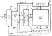
본 발명의 다양한 양상들이 통합된 예시적인 메모리 시스템이 도 1의 블록선도로 일반적으로 예시되어 있다. 도 1의 것과는 다른 구조가 본 발명에 또한 이용될 수 있다. 다수의 개별적으로 어드레스 가능한 메모리 셀들(11)이 로우 및 칼럼 어레이로 배열된다. 어레이(11)의 칼럼을 따라 연장되는 비트라인들이 라인들(15)을 통해 비트 라인 디코더, 드라이버, 및 센스 증폭기들(13)과 전기적으로 연결된다. 어레이(11)의 로우를 따라 연장되는 워드 라인들이 라인들(17)을 통해 워드 라인 디코더 및 드라이버 회로(19)에 전기적으로 연결된다. 어레이(11)의 메모리 셀들의 칼럼을 따라 연장되는 스티어링 게이트들이 라인(23)을 통해 스티어링 게이트 디코더 및 드라이버 회로(21)에 전기적으로 연결된다. 회로(13, 19, 21) 각각은 버스 (25)를 통해 제어기(27)로부터 어드레스들을 수신한다. 디코더 및 드라이버 회로 (13, 19, 21)들은 또한 각각의 제어 및 상태 신호 라인(29, 31, 33)을 통해 제어기(27)에 연결된다. 스티어링 게이트 및 비트 라인에 인가되는 전압들은 제어기와 드라이버 회로(13, 21)을 상호연결하는 버스(22)를 통해 조화(coordination)된다.An exemplary memory system incorporating various aspects of the present invention is generally illustrated in the block diagram of FIG. 1. A structure other than that of FIG. 1 can also be used in the present invention. Multiple individually
제어기(27)는 라인(35)을 통해 호스트 디바이스 (미도시)에 연결될 수 도 있다. 이 호스트 디바이스는 퍼스널 컴퓨터, 노트북 컴퓨터, 휴대용 디바이스, 디지털 카메라, 오디오 플레이어, 셀룰러 폰, 또는 다른 각종 디바이스로 될 수 있다. 도 1의 메모리 시스템은 여러 가지 현재의 전기적 표준들, 예컨대 PCMCIA, CompactFlashTMAccociasion, MMCTMAssociation, SMART MEDIA, Secure DigitalTM, Memory Stick 및 기타들중 어느하나에 따른 카드에서 구현될 수 있다. 카드 포맷인 경우에 라인(35)는 호스트 디바이스의 예비 커넥터와 인터페이스하는 카드 상의 커넥터에서 종단한다. 대안적으로, 도 1의 메모리 시스템은 호스트 컴퓨터에 내장될 수 있다. 또 다른 대안으로서, 제어기(27)는 호스트 디바이스에 내장될 수 있는데 반해, 메모리 시스템의 다른 성분들은 제거가능한 카드에 실장될 수 있다. 다른 실시예들에서, 메모리 시스템은 카드가 아닌 패키징으로 될 수 있다. 예컨대, 메모리 시스템은 하나 이상의 집적회로 또는 하나 이상의 회로 보드 또는 다른 패키지에 실장될 수 있다.The
디코더 및 드라이버 회로(13, 19, 21)는 버스(25)를 통해 어드레스될 때 각각의 제어 및 상태 신호 라인(29, 31, 33)에서의 제어신호에 따라 어레이(11)의 그들 각각의 라인에 적절한 전압을 발생하여 프로그래밍, 판독 및 소거동작을 실행하게 한다. 전압레벨 및 기타 어레이 파라미터를 포함하는 상태 신호들은 어레이(11)에 의해 제어 및 상태 신호 라인 (29, 31, 33)을 통해 제어기(27)에 제공된다. 회로(13) 내의 복수의 센스 증폭기들이 어레이(11) 내의 어드레스된 메모리 셀의 상태를 표시하는 전류 또는 전압레벨을 수신한다. 이 센스 증폭기들은 제어기(27)에, 판독동작 동안 라인(41)을 통해 메모리 셀들의 상태에 관한 정보를 제공한다. 다수의 센스 증폭들이 다수의 메모리셀의 상태들을 병렬로 판독할 수 있도록 하기위해 일반적으로 이용된다.Decoder and
Ⅱ. 메모리 셀II. Memory cell
도 2는 메모리 어레이(11)의 일부분에 대한 일 실시예의 평면도이다. 도 3은 이 메모리 셀을 섹션 A-A를 따라 절취한 부분 단면도이다. 기판 및 도전 요소들이 이들 사이에 존재하는 유전층 들을 덜 상세하게 보인 상태로 도시되어 있다. 이는 도면을 간략화하고자 하는 것으로, 도전층들 간의 사이 및 도전층과 기판사이에 적절한 산화물층들이 포함될 수 있음을 이해할 수 있을 것이다2 is a plan view of one embodiment of a portion of the
실리콘 기판(45)은 평평한 상부표면(47)을 포함한다. 연장된 확산부(49, 51, 53)가 초기의 이온주입 및 후속의 확산에 의해 상기 표면(47)을 통해 기판(45)내로 형성된다. 연장된 확산부(49,51,53)는 메모리 셀의 소오스 및 드레인 역할을 한다. 이들에 대한 설명을 위해, 확산부들은 제 1의 "x" 방향으로 이격되고 그리고 길이가 제 2의 "y"방향으로 연장되는 상태로 도시되어 있다. 이들 "x" 및 "y" 방향은 실질적으로 서로 직교한다. 다수의 부동 게이트들이 기판표면(47)에 걸쳐 포함되어 있으며, 로우 및 컬럼의 어레이에서 그들 사이에 적절한 게이트 유전체들이 형성되어있다. 부동 게이트(55,56,57,58,59,60)의 한 로우는 부동 게이트(62,63,64,65,66,67)의 다른 로우에 인접하여 서로 평행을 이룬다. 부동 게이트(69, 55, 62, 71, 73)의 칼럼은 부동 게이트(75, 56, 63, 77, 79)의 칼럼에 인접하여 서로 평행을 이룬다. 이 부동 게이트들은 도전적으로 도핑된 폴리크리스탈린 실리콘("폴리실리콘")의 제 1층으로부터 형성되는데, 이 층은 상기 표면상에 증착된 후 하나 이상의 마스킹 단계를 이용한 에칭에 의해 개별 부동 게이트로 분할된다.The
비트 라인 디코더 및 드라이버 회로(13)(도 1참조)는 라인(15)을 통해, 도 2 및 도 3의 확산부(49,51,53)를 포함하는 어레이의 비트라인 소오스/드레인 확산부 모두와 연결된다. 개별 메모리 셀의 칼럼의 소오스 및 드레인은, 버스(25)를 통해 공급되는 어드레스들 및 라인(29)을 통한 제어신호에 응답하여 판독 또는 프로그래밍을 위한 적절한 동작전압에 연결된다.The bit line decoder and driver circuit 13 (see FIG. 1) is connected via
도 2 및 3의 구조는 부동 게이트의 2개의 칼럼마다 하나의 스티어링 게이트를 이용한다. 스티어링 게이트(81, 83, 85)는 "Y"방향으로 연장되며, 부동 게이트의 2개의 인접 칼럼과 이 칼럼 사이에 위치되는 소오스/드레인 확산부에 걸쳐 확장하는 "X"방향으로의 폭을 구비한다. 스티어링 게이트중 어떤 2개의 게이트사이의 간격은 적어도 2개의 스티어링 게이트에 의해 오버레이 되는 부동 게이트의 인접 칼럼사이에서 x"방향으로의 공간만큼 큼으로써, 이 공간에서 기판에 게이트가 형성될 수 있게 된다. 스티어링 게이트들은 도전적으로 도핑된 폴리실리콘의 제 2층을 에칭함으로써 형성되는데, 이 제 2층은 상기 제 1 폴리실리콘 층 및 적절한 인터폴리실리콘층 유전체에 걸친 전체 표면 위에 형성된다. 스티어링 게이트 디코더 및 드라이버 회로(21)(도 1 참조)는 라인(23)을 통해 모든 스티어링 게이트에 연결되며, 버스(25)상에 제공되는 어드레스들, 라인(33)상의 제어신호, 및 드라이버들 및 감지 증폭기(13)로부터의 데이터에 응답하여 그들의 전압을 개별적으로 제어한다.2 and 3 use one steering gate for every two columns of the floating gate. The
도 2 및 도 3의 워드라인(91,92,93,94,95)은 "x"방향으로 연장되며, 각 워드 라인을 프로팅 게이트의 로우와 정렬하는 "y"방향에서 그들 간의 공간을 둔채 스티어링 게이트들에 걸쳐 연장된다. 이 워드 라인들은 도전적으로 도핑된 폴리실리콘의 제 3층을 에칭함으로써 형성되는데, 이 제 3층은 먼저 제 2 폴리실리콘층위에 형성된 유전체의 상부 상의 전체 표면 및 스티어링 게이트들 간의 노출된 영역들에 증착된다. 이 워드 라인들은 판독 및 기입을 위한 그의 로우에서 모든 메모리셀들을 선택할 수 있게 한다. 선택 게이트 디코더 및 드라이버회로(19)(도 1)는 메모리 어레이의 1개의 로우를 개별적으로 선택할 수 있도록 각 워드라인과 연결된다. 선택된 로우 내의 개별 셀들은 이제 비트라인 및 스트어링 디코더 및 드라이버 회로(13, 21)(도 1)에 의한 판독 및 기입을 위해 인에이블된다.The word lines 91, 92, 93, 94 and 95 of Figs. 2 and 3 extend in the " x " direction, with a space therebetween in the " y " direction that aligns each word line with the row of the floating gate. Extends across the steering gates. These word lines are formed by etching a third layer of conductively doped polysilicon, which is first deposited on the entire surface on top of the dielectric formed over the second polysilicon layer and the exposed areas between the steering gates. do. These word lines allow all memory cells to be selected in their row for reading and writing. The select gate decoder and driver circuit 19 (FIG. 1) is connected to each word line to individually select one row of the memory array. Individual cells in the selected row are now enabled for reading and writing by the bitline and steering decoder and
상기 구조에서의 게이트들은 도핑된 폴리실리콘 물질로 만들어지지만은, 다른 적절한 전기적으로 도전성인 물질이 전술한 3개의 폴리실리콘층 중 하나 이상을 대체하여 사용될 수 있다. 워드 라인 및 선택 게이트를 형성하는 상기 제 3층은 예컨대, 그의 도전성을 증가시키기 위하여 그의 상부에 텅스텐과 같은 그러한 도전성의 고융점 금속 실리사이드를 갖는 폴리실리콘인 폴리사이드 물질로 될 수도 있다. 폴리사이드들은 일반적으로 제 1 또는 제 2 폴리 실리콘층을 대체하여 사용되지 않는데, 그 이유는 폴리 사이드로부터 형성된 인터폴리 다결정 실리콘 산화물의 물질은 만족스럽지 못하기 때문이다.Although the gates in the structure are made of doped polysilicon material, other suitable electrically conductive materials may be used in place of one or more of the three polysilicon layers described above. The third layer forming the word line and the select gate may be a polyside material, for example polysilicon having such a conductive high melting point metal silicide such as tungsten on top thereof to increase its conductivity. Polysides are generally not used in place of the first or second polysilicon layer because the material of the interpoly polycrystalline silicon oxide formed from the polyside is not satisfactory.
금속 컨덕터층들은 도 2 및 3에 도시되지 않았다. 확산부 및 폴리실리콘 요소들은 일반적으로 금속보다 도전성이 상당히 낮기 때문에, 금속 컨덕터들은 폴리실리콘 요소 및 확산부의 길이를 따라 주기적인 간격으로 어떤 중간 층을 통하여 각 금속 라인들에 형성되는 연결부들을 갖는 개별 층들에 포함된다. 도 2 및 3의 실시예의 확산부 및 폴리실리콘 요소들 모두는 개별적으로 구동될 필요가 있으므로, 전형적으로 이들 금속 라인들의 수와 상기 확산부 및 폴리실리콘 요소의 수가 1 대 1로 대응되게 한다.Metal conductor layers are not shown in FIGS. 2 and 3. Since the diffusion and polysilicon elements are generally considerably less conductive than metal, the metal conductors have separate layers with connections formed in the respective metal lines through some intermediate layer at periodic intervals along the length of the polysilicon element and the diffusion. Included in Both the diffuser and polysilicon elements of the embodiment of FIGS. 2 and 3 need to be driven separately, so that typically the number of these metal lines and the number of diffuser and polysilicon elements correspond one to one.
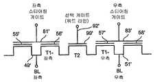
도 4는 도 3의 구조에 대한 전기적 등가 회로를 도시한 것으로서, 여기서 도 2 및 3에서의 동일한 요소들에 대해서는 동일한 도면부호로 표기하되 도면부호에 프라임(')을 붙였다. 도시된 구조는 이웃구조들과 소오스 및 드레인 확산부를 공유한다. 기판에서 인접 확산부(49, 51)간의 채널을 통한 도통은 3개의 서로다른 영역에서 서로다른 게이트 요소에 의해 제어된다. 좌측의 제 1 영역(T1-좌측)은 자신 바로위에 놓이는 부동게이트(56)와 그리고 자신과 용량적으로 결합된 스티어링 게이트(81)을 구비한다. 우측의 제 2영역(T1-우측)은 마찬가지 방식으로 부동 게이트(57) 및 스티어링 게이트(83)에 의해 제어된다. T1-좌측과 T1-우측 사이의 제 3영역 T2는 워드라인(92)의 부분인 선택 게이트(99)에 의해 제어된다.FIG. 4 shows an electrical equivalent circuit for the structure of FIG. 3, wherein like elements in FIGS. 2 and 3 are denoted by the same reference numerals, but with a prime ('). The illustrated structure shares source and drain diffusions with neighboring structures. Conduction through the channel between adjacent diffusions 49 and 51 in the substrate is controlled by different gate elements in three different regions. The first region (T1-left) on the left side has a floating
확산부(49, 51)사이의 채널을 통한 전자들의 도통 레벨은 따라서 이들의 서로다른 게이트 요소들에 의해 그들 각각의 채널영역에 제공되는 전계에 의해 이들 게이트에 놓이는 전압만큼 영향을 받게 된다. 부동 게이트상의 전압은 이 게이트가 운반하는 순수 전하의 레벨 및 다른 게이트 및 노드들로부터 용량적으로 결합되는 모든 변위 전하에 의해 좌우되게 된다. 부동 게이트하의 채널부를 통해 허용되는 도통의 레벨은 그 부동 게이트상의 전압에 의해 제어된다. 선택 게이트(99)상의 전압은 이 채널들을 임의의 도통 상태로 간단히 턴온 및 턴오프하여, 그들의 소오스/드레인 영역과 연결을 위한 개별 셀들을 선택한다. 일 실시예에서, 개별 메모리 셀은 채널의 3개의 서로 다른 영역들 (T1-좌측, T2, T1-우측) 각각에 대해 하나씩 3개의 트랜지스터들의 직렬 연결로서 간주될 수 있다. 다른 실시예에서, 각 부동 게이트는 메모리 셀로서 간주될 수 있다.The conduction level of the electrons through the channel between the diffusions 49 and 51 is thus influenced by the voltages placed on these gates by the electric field provided to their respective channel regions by their different gate elements. The voltage on the floating gate is governed by the level of pure charge carried by the gate and any displacement charge that is capacitively coupled from other gates and nodes. The level of conduction allowed through the channel portion under the floating gate is controlled by the voltage on the floating gate. The voltage on
단일 메모리 셀의 2개의 부동 게이트중 하나는 (그의 상태와 관계하는) 전하가 다른 부동 게이트에 의해 유지된다 하더라도 다른 부동 게이트하의 채널영역이 충분히 도통되게 하기에 충분한 셀의 다른(비선택된) 부동 게이트 상의 스티어링 게이트에 전압을 인가함으로써 프로그래밍 혹은 소거를 위해 선택된다. 그 셀의 선택 트랜지스터가 그의 워드 라인에 인가되는 충분한 전압에 의해 턴온되면, 단지 그 선택된 부동 게이트만이 상기 셀에 대한 판독 또는 프로그래밍 동작에 응답하게 된다. 상기 하나의 부동 게이트 상태의 판독 시, 그의 소오스와 드레인 사이에서의 상기 셀을 통한 전류는 따라서 상기 다른 부동 게이트상의 전하에 관계없이 상기 선택된 부동 게이트에 의해 유지되는 전하에 의존하게 된다. 비선택된 부동 게이트하의 채널부가 도통되게 하기 위해 비선택된 부동 게이트상의 스티어링 게이트에 인가되는 전압은 또한 동일 스티어링 게이트를 통해 인접 셀의 인접 부동게이트에 결합되지만은, 상기 인접 셀의 다른 요소들에 적절한 전압조건을 유지함으로써 인접셀들에 대한 영향이 회피될 수 있다.One of the two floating gates of a single memory cell is the other (non-selected) floating gate of the cell sufficient to allow the channel region under the other floating gate to conduct sufficiently even though the charge (relative to its state) is held by the other floating gate. It is selected for programming or erasing by applying a voltage to the steering gate of the phase. If the select transistor of that cell is turned on by a sufficient voltage applied to its word line, then only the selected floating gate will respond to a read or program operation for that cell. Upon reading of the one floating gate state, the current through the cell between its source and drain is thus dependent on the charge held by the selected floating gate regardless of the charge on the other floating gate. The voltage applied to the steering gate on the unselected floating gate to allow the channel portion under the unselected floating gate to conduct is also coupled to the adjacent floating gate of the adjacent cell through the same steering gate, but with a voltage suitable for other elements of the adjacent cell. By maintaining the condition, the effect on adjacent cells can be avoided.
도 2 내지 도 4 실시예의 부동 게이트들은 비트라인(소오스 및 드레인 확산부)에, 그리고 기판 채널영역에서 충분한 에너지를 얻도록 전자들이 게이트유전체에 걸쳐 선택된 부동게이트로 주입되도록 하는 2개의 스티어링 게이트들에 전압을 인가함으로써 옳바르게 프로그래밍된다. 이를 위한 옳바른 기술은 참고문헌으로서 본원에 인용하는 미국특허번호 5,313,421 및 5,712,180에 기술된 "소오스측 주입"이다.The floating gates of the Figures 2-4 embodiment are at the bit line (source and drain diffuser) and at the two steering gates which allow electrons to be injected into the selected floating gate across the gate dielectric to obtain sufficient energy in the substrate channel region. Correctly programmed by applying a voltage. The correct technique for this is the "source side injection" described in US Pat. Nos. 5,313,421 and 5,712,180, which are incorporated herein by reference.
도 2 내지 4 실시예의 메모리 셀들을 소거하기 위해, 이들은 선택된 부동 게이트로부터 워드 라인의 선택 게이트 또는 채널로의 전자들이 이동되도록 설계되어 동작된다. 만일 선택 게이트에 대해 소거되는 경우, 부동 게이트 에지(103)와 선택 게이트(99)사이의 유전체는 부동 게이트 에지 상에 성장되고 그리고 적절한 전압들이 셀의 다양한 요소들 상에 놓일 때 전자들이 터널링하게 되는 박막 산화물층이 된다. 이는 부동 게이트 에지(105)와 선택 게이트(99) 사이에 제공된다. 선택 게이트(99)에 대해 소거되도록 설계할 때, 선택 게이트와 기판 표면(47) 사이의 게이트 유전체에 걸친 결과적인 전압 기울기는 그 유전체의 브레이크다운 레벨보다 충분히 낮게 유지되도록 해야한다. 이는 워드 라인은 전형적으로 소거 동안 10V로 때로는 20V 또는 그 이상울 초과하는 레벨로 상승하는데 반해, 셀에 인가되는 다른 전압들은 일반적으로 5V이하이기 때문이다. 선택 게이트 유전체에 걸친 전압 기울기는 이를 두껍게 만듦으로써 감소될 수 있거나 또는 보통 이용되는 것보다 높은 유전 상수를 갖도록 선택될 수 있으나, 이는 선택 트랜지스터의 동작에 악영향을 끼칠 수 있다.To erase the memory cells of the Figures 2-4 embodiment, they are designed and operated so that electrons from the selected floating gate to the select gate or channel of the word line are moved. If erased for the select gate, the dielectric between the floating
만일 셀이 채널에 대해 소거되는 경우, 도 2내지 4의 실시예는 다소 변경된다. 먼저, 선택 게이트(99)와 인접 부동게이트에지(103,105)사이의 유전체는 부동게이트가 선택게이트에 대해 소거되는 것을 방지하도록 두껍게 만들어진다. 둘째, 부동게이트의 하부층과 기판표면(47)사이의 게이트 유전체의 두께는 그를 통한 전자 터널링이 용이하도록 약 100옹스트롱 정도로 얇게 만들어진다. 셋째, 블록으로서 동시에 소거될 셀이 칼럼을 따라 혹은 블록내에서 서로 그룹지어진다. 일실시예에서, 한 블록이 기판에서 다른 블록과 분리된다. 이는 전형적으로 트리플 웰 프로세스에 의해 이루어지며, 여기서 n-웰이 p-기판에 형성되고, 셀의 블록을 유지하는 p-웰이 이 블록을 다른 것으로부터 분리시키는 n-웰 내에 위치된다. 이어서, 적절한 소거전압이 소거될 블록의 p-웰 에 인가되고, 다른 블록들은 영향을 받지 않는다.If the cell is erased for the channel, the embodiment of Figures 2-4 is somewhat modified. First, the dielectric between the
도 1내지 5의 구조에 관한 보다 구체적인 설명이 참고문헌으로서 본원에 인용하는 미국특허 6,151,248에 기재되어 있다. 도 2내지 4의 메모리구조는 적절한 메모리셀의 한 예이다. 다른 구조들이 또한 본 발명을 구현하는데 이용될 수있다. 예컨대, 일실시예는 전하저장 유전체를 포함하는 다중층 유전체를 이용할 수 있다.A more detailed description of the structure of FIGS. 1-5 is described in US Pat. No. 6,151,248, which is incorporated herein by reference. 2-4 is one example of a suitable memory cell. Other structures may also be used to implement the present invention. For example, one embodiment may use a multilayer dielectric including a charge storage dielectric.
Ⅲ. 메모리 어레이 동작III. Memory Array Behavior
어레이(11)의 메모리셀들을 프로그래밍, 판독 및 소거하는 예시적인 동작전압이 도 5의 테이블에 나타나있다. 라인(2)은 선택 게이트(워드라인)에 대해 소거되는 셀의 타입의 동작에 관한 것이고, 라인(8)은 기판에 대해 소거되는 셀의 타입을 동작시키는 변형을 보인 것이다. 이들 예에서, 셀이 형성된 기판부는 p-타입 도핑을 포함하며, 비트라인 확산부는 n-타입으로되어 있다. 기판은 이들 동작을 통하여 접지전위로 유지된다.Exemplary operating voltages for programming, reading, and erasing memory cells of the
도 5 테이블의 라인(1)에서, 선택되지않은 로우에 대해 전압조건이 주어진다. 비선택 로우의 워드라인은 드라이버회로(19)(도1)에 의해 접지전위에 놓인다. 비선택 로우를 따른 셀의 비트라인(확산부)과 스티어링 게이트들에 대한 칼럼들에서의 "x"는 이들 요소에서의 전압들은 "돈 케어(don't care)상황임을 표시한다. 본 예에서, 어레이의 요소들에 대한 회로(13,19,21)중 어느것에 의해 발생되는 네거티브 전압이 없기 때문에, 로우의 선택 게이트에서의 제로(0)전압은 그 로우를 따른 셀들중 어느 것도 인에이블되지 않게 한다. 이들의 채널에는 전류가 흐르지 않는다. 다른 로우의 동일 칼럼들에 있는 다른 셀들의 프로그래밍 또는 판독은 그의 워드라인상에서 제로 전압을 갖는 로우에 영향을 끼침이 없이 이루어 질 수 있다.In
테이블에서 제 2라인(2)은 워드라인의 선택게이트에 대해 소거되도록 설계된 셀의 타입을 소거하기위한 예시적인 전압 세트를 제공한다. 10 - 25V의 범위에 있는 높은 소거전압 VE (예컨대, 20V)이 드라이버회로(19)에 의해 (부동게이트가 소거될)모든 워드라인에 인가된다. 이는 일반적으로, 다수의 연속적인 로우에서의 모든 셀을 포함하는 셀들의 적어도 하나의 정의된 블록이다. 그러나, 바람직한 응용들에서, 소수의 또는 더 많은 셀들이 동시에 소거될 수도 있다. 대안적으로, 소거 블록은 셀들의 단일 로우로 국한 될 수도 있다. 하나 이상의 선택된 로우를 따르는 셀들의 스티어링 게이트는, 스티어링 게이트와 부동게이트 사이의 높은 용량성 결합에 의해 부동게이트의 전압을 낮은 레벨로 유지하도록 드라이버회로(21)에 의해 낮은 전압(예컨대, 0V)으로 설정된다. 부동게이트와 이들의 각각의 선택 게이트(워드라인)간의 결과적인 전위차는 중간 유전체를 통한 전자 터널링을 일으킨다. 소거에 관한 많은 정보를 참고문헌으로서 본원에 인용하는 미국특허 5,270,979에서 찾아볼 수 있다.The
도 5의 테이블에서 라인(3) 및 라인(4)은 메모리 셀의 2개의 부동 게이트의 상태를 판독하기위한 예시적인 전압을 제공하는 바, 라인(3)은 좌측 부동게이트에 대한 것이고, 라인(4)은 우측 부동게이트에 대한 것이다. 각 경우에, 셀은 셀의 선택 트랜지스터를 턴온시켜 전류가 채널을 통하여 흐르게 하기에 충분한 전압(VSR)으로 상승되는 선택 게이트 전압에 의해 인에이블된다. 이 전압은 전형적으로 선택 트랜지스터의 임계 전압보다 1V 높다.
하나의 부동게이트의 전압상태를 판독할 때, 판독되는 부동 게이트 위의 스티어링 게이트에는 전압(VM)이 인가되며, 다른 부동 게이트위의 스티어링 게이트는 도 5 테이블의 라인(3) 및 (4)에 보인바와같이 전압(VBR)로 상승된다. 전압(VBR)은 비선택된 부동게이트의 프로그래밍된 상태에 관계없이 비선택된 부동게이트 아래의 셀의 채널부가 충분히 도통되도록 하기에 충분히 높게(예컨대, 8V)된다. 선택된 부동 게이트의 상태를 판독하기위해, 전압(VM)이 판독단계동안 (하기에 설명하는)다중 전압을 통하여 스텝되며, 셀전류가 정의된 임계 전압을 통과할 때 그의 값은 회로(13)내의 센스 증폭기에 의해 검출된다.When reading the voltage state of one floating gate, a voltage VM is applied to the steering gate on the floating gate being read, and the steering gate on the other floating gate is connected to
이중(dual) 부동 게이트 셀의 하나의 부동 게이트를 프로그래밍하는 예시적인 전압들이 도 5의 테이블의 라인(5 및 6)에 주어진다. 동작을 위한 셀을 선택하기 위해, 선택 게이트는 셀의 선택 트랜지스터를 턴온하기에 충분하도록 승압된다. 소스측 주입 프로그래밍 속도를 최적화하기 위해, 전압 VSP는 판독 동안에 사용되는 전압 VSR과 서로 다르다. 예로서, 선택 트랜지스터의 임계 전압값이 1V(volt)일때 VSP=2.2V이다. 프로그래밍되도록 선택된 부동 게이트와 셀의 동일 측 상의 비트라인 확산은 프로그래밍 동작 동안에 최대 비트라인 전압(예를 들어, 5V)으로 승압된다. 소스측 열전자 프로그래밍을 얻기 위해 부동 및 선택 게이트 채널 사이의 갭 양단에 충분한 전계가 생성되도록 상기 전압은 매우 커야 한다. 비 선택 부동 게이트와 셀의 동일 측 상의 비트라인 확산은 프로그래밍 동안에 0V 또는 거의 0V로 바이어스된다.Example voltages for programming one floating gate of a dual floating gate cell are given in
부동 게이트 전압의 프로그래밍 윈도우 범위 내에서 비선택 부동 게이트 상에 어떤 부동 게이트 전압이 존재하는지에 무관하게 타겟 부동 게이트의 프로그랭에 어떠한 혼선도 주지 않기 위해, 비선택 부동 게이트 위의 스트어링 게이트는 비선택 부동 게이트 아래의 채널 영역이 충분히 전도성이 되는데 충분한 전압 VBP(예를 들어, VBP=8V)로 승압된다. 선택 부동 게이트가 열전자 프로그래밍을 위해 선택 부동 게이트 아래의 채널에서 바람직한 전계 조건을 생성하는데 도움을 주는 전압이 되도록 하는 레벨의 전압(VP)이 선택 부동 게이트 위의 스티어링 게이트에 인가된다. 예를 들어, 전압(VP)은 5-12V 범위 내일 수 있다. 이 전압은 프로그래밍 동작 동안에 변할 수 있다. 일반적으로, 적당한 프로그래밍 전압 세트가 우선 소거셀로 인가되고 그 다음 적당한 판독 전압 세트가 인가되며, 만약 판독 단계에서 선택 부동 게이가 바람직한 전압 상태(이는 이진 저장을 위한 프로그래밍 상태이거나 다중 레벨 저장을 위한 가변 저장 상태 중 하나일 수 있음)로 프로그래밍되었다고 표시하지 않는다면, 이전의 세트와는 부분적으로 서로 다를 수 있는 프로그래밍 전압들이 다시 인가된다.The sting gates on the non-selected floating gates are non-crossed to avoid any cross-talk to the target of the floating gate voltage regardless of what floating gate voltage is present on the non-selected floating gates within the programming window range of the floating gate voltage. The channel region under the select floating gate is stepped up to a sufficient voltage VBP (eg, VBP = 8V) to be sufficiently conductive. A voltage VP at a level is applied to the steering gate above the selection floating gate such that the selection floating gate is a voltage that helps to create the desired field conditions in the channel below the selection floating gate for thermoelectronic programming. For example, the voltage VP may be in the range 5-12V. This voltage can change during a programming operation. In general, a suitable set of programming voltages is first applied to the erase cell and then a suitable set of read voltages is applied, and if a selective floating gay is desired in the read phase, this can be a programming state for binary storage or a variable for multilevel storage. Programming voltages, which may be partially different from the previous set, are again applied unless otherwise indicated as being programmed.
도 5의 테이블의 라인(7)은 스스로 프로그래밍되지 않는 프로그래밍을 위해 선택된 로우 내의 셀들에 인가된 전압들을 도시한다. 예를 들어, 어레이의 분리된 일부분의 하나의 로우에서 동시에 프로그래밍되는 셀의 갯수는 로우에 따라 그들 사이에 프로그래밍되지 않는 다른 셀들과 함께 교대로 위치한다. 프로그래밍되지 않는 이들 다른 셀들은 도 5의 테이블의 라인(7)의 전압을 받는다. 채널에서 어떠한 전류의 흐름도 방지하기 위해 반대 비트라인 확산들은 동일한 전압(예를 들어, 모두 0V 또는 5V)에 유지된다. 라인(1)에서 사용되는 바와 같이, "X"는 이러한 셀들의 스티어링 게이트들 상의 전압이 어떤 것이든 상관없음을 나타낸다.
기판에 소거되도록 디자인된 메모리 어레이의 경우에, 라인(8)의 소거 전압 조건들이 라인(2)의 것들에 대신해서 인가된다. 소거될 셀들의 블록을 포함하는 p-웰과 이를 둘러싸는 n-웰 모두는 예시적인 10-25V 범위 내의 소거 전압(VE)(예를 들어, 바람직하게 20V)으로 승압된다. 이러한 셀들의 판독 및 프로그래밍 동안에, 이들의 웰들은 그라운드 전위로 유지된다. 선택 게이트 유전체 양단에 인가된 전압을 줄이기 위해 바람직하게 양의 전압(VSE)이 선택 게이트에 인가되는바, 이는 기판과 선택 게이트 사이의 초과 전압 차이가 유전체 물질을 손상시키거나 유전체 물질을 셀들의 동작을 위해 바람직한 것보다 더욱 두껍게 만들 수 있기 때문이다. 이러한 전압이 부분적으로 선택 게이트로부터 소거되도록 하는 인접한 부동 게이트들로 결합되기 때문에, 이는 매우 높을 수 없으며 그렇지 않으면 소거를 완수하기 위해 매우 높은 부동 게이트들과 기판 채널 상의 전압 차이가 매우 낮아진다. VE의 레벨에 따라 VSE의 예시적인 범위는 3-12V이다. VE=20V일 때 VSE=10V가 바람직하다.In the case of a memory array designed to be erased to a substrate, erase voltage conditions of line 8 are applied instead of those of
도 5에 제공되는 값들은 하나의 예시적인 세트이다. 기술분야의 당업자는 메모리 시스템을 동작하게 하는 다른 적당한 값들 및 방법들을 사용할 수 있을 것이 다.The values provided in FIG. 5 are one exemplary set. Those skilled in the art will be able to use other suitable values and methods for operating the memory system.
IV. 트래킹 셀(Tracking Cell)IV. Tracking Cell
전술한 바와 같이, 부동 게이트들은 다중 레벨들 또는 범위의 전하를 저장할 수 있고, 이에 따라 다중 상태를 제공할 수 있다. 일 예시에서, 부동 게이트는 8 개의 타겟 전하 범위들을 저장할 수 있다. 따라서, 8개의 상태를 제공할 수 있다. 이러한 부동 게이트는 3비트의 데이터를 저장한다. 도 6은 8개의 상태들을 저장할 수 있는 부동 게이트에 대한 예시적인 상태 공간을 그래프로 도시한다. 도 6은 8개의 물리적 상태:P0, P1, P2, P3, P4, P5, P6, 및 P7를 도시한다. 예시적인 목적으로, 도 6에서 수직 축은 mV(milivolts) 단위로서 임계 전압이다. 그러나, 실시에 따라 다른 단위들이 사용될 수 있다. 물리적 상태들 각각에 대해서, 도 6은 종모양 곡선으로 나타나는 임계 전압 레벨들의 범위 또는 분포를 도시한다. 종모양 곡선의 정상(즉, 최우측 포인트)은 일반적으로 상태의 중앙을 나타낸다. 예를 들어, 상태(P1)는 상태의 중앙이 1,000mV에 있고, 하측 경계는 800mV이고 상측 경계는 1,200mV이다. 상태들 사이의 영역은 상태 사이의 임계 마진으로 알려져 있다. 7개의 임계 마진이 존재하고, 이들은 각각 인접하는 상태 세트들 사이에 존재한다. 예를 들어, 인접하는 상태들(P1 및 P2) 사이에 임계 마진이 존재한다. 도 6에서 P0가 음의 전압을 포함하는 반면에 상태들(P1-P7)이 양의 전압임을 주목해라. 다른 실시예에서, 더 많은 또는 더 적은 상태들이 양 또는 음일 수 있다. 추가로, 0 내지 4,900mV의 전압 범위는 메모리 어레이의 특정 특성 및 조건들에 따라 다양한 실시예들에서 서로 다른 수 있다.As mentioned above, floating gates can store multiple levels or range of charges and thus provide multiple states. In one example, the floating gate can store eight target charge ranges. Thus, eight states can be provided. This floating gate stores three bits of data. 6 graphically illustrates an example state space for a floating gate that can store eight states. 6 shows eight physical states: P0, P1, P2, P3, P4, P5, P6, and P7. For illustrative purposes, the vertical axis in FIG. 6 is the threshold voltage in millivolts (mV). However, other units may be used depending on the implementation. For each of the physical states, FIG. 6 shows the range or distribution of threshold voltage levels represented by a bell curve. The top (ie rightmost point) of the bell curve generally represents the center of the condition. For example, state P1 is at the center of the state at 1,000 mV, the lower boundary is 800 mV and the upper boundary is 1,200 mV. The area between states is known as the threshold margin between states. There are seven threshold margins, each of which exists between adjacent state sets. For example, there is a threshold margin between adjacent states P1 and P2. Note that in FIG. 6 the states P1-P7 are positive voltages while P0 contains a negative voltage. In other embodiments, more or fewer states may be positive or negative. In addition, the voltage range of 0-4900 mV may be different in various embodiments depending on the specific characteristics and conditions of the memory array.
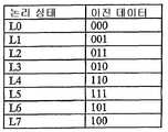
8개의 상태들을 저장하는 부동 게이트는 3 비트 만큼의 데이터를 저장할 수 있다. 따라서, 8개의 논리 상태들이 존재한다. 일 실시예에서, 이러한 논리 상태들은 그레이 코드 할당을 사용하여 물리적 상태들에 할당되어, 만약 부동 게이트의 임계 전압이 잘못하여 인접한 물리적 상태로 천이되더라도, 오로지 하나의 비트만이 영향을 받게 될 것이다. 도 7은 이진 데이터의 논리 상태로의 예시적인 그레이 코드 할당을 도시하는 테이블을 제공한다. 다른 실시예에서, 비 그레이 코드(non-gray code) 할당이 또한 사용될 수 있다. 각 논리 상태는 물리 상태로 할당된다. 그러나, 논리 상태의 물리 상태로의 할당은 로테이션될 수 있다. 도 8은 논리 상태의 물리 상태로의 할당을 위한 8개의 서로 다른 로테이션 방식을 도시하는 다이어그램이다. 예를 들어, 로테이션(0)에서, 물리 상태(P0)는 논리 상태(L0)(예를 들어, 이진 데이터 000)를 저장하고, 물리 상태(P1)는 논리 상태(L1)(예를 들어, 이진 데이터 001)를 저장하는 식이다. 로테이션(1)에서, 물리 상태(P0)는 논리 상태(L7)(예를 들어, 이진 데이터 100)를 저장하고, 물리 상태(P1)는 논리 상태(L0)(예를 들어, 이진 데이터 000)를 저장하는 식이다. 따라서, 프로그래밍시에 사용될 수 있는 8개의 서로 다른 로테이션 방식이 존재한다. 본 발명의 일 실시예에서, 각 시간마다 한 섹터가 프로그래밍되며, 이 섹터는 우선 소거되고 그 다음 8개의 로테이션 방식들 중 하나로 프로그래밍된다. 후속 프로그래밍/소거 사이클들에서, 상기 섹터는 다른 로테이션 방식으로 프로그래밍될 것이다. 일 실시에서, 메모리 장치는 연속적으로 로테이션 상태들을 통해 사이클링할 것이다. 다른 실시예에서, 메모리 장치는 각 프로그래밍 사이클에 대해서 로테이션 방식을 무작위적으로(의사-무작위적으로(pseudo-randomly)) 선택할 것이다. 데이터를 로테이션하는 것은 반복적인 프로그래밍-소거 사이클 동안에 섹터로 프로그래밍될 실제 데이터 패턴에 무관하게 섹터 내의 모든 셀들에 대해 균일한 스트레스 조건들을 유지하도록 한다. 데이터의 로테이션에 관해서, 일 실시예에서 동일한 포스트-소거 로테이션(post-erase rotation)이 주어진 소거-블록들에 대한 모든 섹터들로 전파될 수 있는바, 이는 모든 이러한 섹터들이 이력에 조화(history-unison)를 이루어 동작하기 때문이다. 또한, 만약 내부 섹터 소모의 균등화(intra-sector wear leveling)이 부적절하다면, 일부 형태의 강제 프로그래밍(forced programmed) 내부 섹터 소모의 균등화가 필요하다(예를 들어, 일부 강제 레벨이나 논리 데이터 패턴으로 간헐적인 프로그래밍).The floating gate, which stores eight states, can store as many as three bits of data. Thus, there are eight logic states. In one embodiment, these logic states are assigned to physical states using gray code assignment so that only one bit will be affected if the threshold voltage of the floating gate accidentally transitions to an adjacent physical state. 7 provides a table illustrating exemplary gray code assignment of binary data to a logical state. In other embodiments, non-gray code assignments may also be used. Each logical state is assigned a physical state. However, the assignment of the logical state to the physical state can be rotated. 8 is a diagram illustrating eight different rotation schemes for assignment of logical states to physical states. For example, in
일 예시에서, 메모리 어레이(11)는 섹터들로 분할된다. 어떻게 섹터가 분할되었는지에 대한 일 실시예가 도 9에 도시된다. 섹터는 사용자 데이터(250)와 ECC 데이터(252)를 포함한다. 일반적으로, 섹터는 512 바이트의 사용자 데이터를 저장할 수 있는 워드라인 상의 셀들의 서브세트(subset of cell)으로 구성된다. 섹터에 대한 다른 정의들이 또한 본 발명에 대해서 사용될 수 있다. 섹터는 또한 트래킹 셀들(254)과 헤더 정보(256)(사용자에 의해 직접 지시되지 않은)를 포함한다. 헤더 정보는 어드레스 정보, 비트 및/또는 섹터 매핑 관련 정보, 그리고 섹터로의 쓰기 갯수의 카운트(count)를 포함한다. 다른 정보에 대해서도 헤더에 유지할 수 있다 트킹 셀들의 예들은 U.S 특허 번호 5,172,338, 6,222,762 및 6,538,922에서 개시되며; 이들 모두는 그 자체로서 본 명세서에 참조로서 통합된다. 트래킹 셀들은 부동 게이트들에서 전하의 다양한 상태들 각각에 대한 최적의 식별 포인트들을 신빙성 있게 확립하는데 사용된다. 도 9에 도시된 실시예에서, 섹터는 24개의 트래킹 셀들을 포함한다. 트래킹 셀들은 쌍들(pairs)로 그룹핑(grouping)되고 세 개의 쌍들이 한 세트로 다시 그룹핑된다. 일 실시예에서, 각 쌍들은 동일한 섹터 내의 부동 게이트들 쌍을 포함하며, 부동 게이트들은 도 2-4에 관해 전술한 바와 같다. 도 9는 트래킹 셀들의 4 개 세트: 세트 260, 세트 262, 세트 264 및 세트 266를 도시한다. 일 실시예에서, 상기 세트들은 동일 정보의 리던던트 카피(redundant copy)이다.In one example,
일 실시예에서, 트래킹 셀들은 단지 두 개의 상태들 중 하나에 데이터를 저장할 뿐이다. 예를 들어, 도 9는 물리 상태(P1) 또는 물리 상태(P6)에 데이터를 저장하는 각 트래킹 셀을 도시한다. 다른 실시예에서, 다른 상태들이 사용될 수 있다. 수많은 실시예에서, 모든 상태들 미만의 상태들이 사용된다. 예를 들어, 도 6은 8개 상태들을 구비한 메모리 상태 공간을 도시한다. 따라서, 본 발명은 트래킹 셀들에 대한 8개 미만의 상태들을 사용한다. 상태들의 서브세트을 사용하는 것의 장점은 사용되는 상태들이 이들 사이에 하나 이상의 상태들로 분리될 수 있다는 점이다. 서로 다른 관련 동작 조건이나 필요조건들 때문에 서로 다른 임계 전압 분포 통계치를 갖는 두 개의 종단 상태들(상태 P0 및 상태 P7)을 피하면서 최대 기준선(baseline)을 제공하도록 임계 전압 레벨에서 가능한 멀리 떨어진 상태들(P1 및 P6)의 선택이 고려될 수 있다. 예를 들어, 상태(P0)는 데이터 프로그래밍의 통계와는 반대되는 소거 동작의 통계를 따른다. 최고로 빈번하게 프로그래밍된 상태(상태 P7)의 경우에 리렉스드 마진(relaxed margin)에 대한 전위가 중간 상태들(P1-P6)에 대해 분포에 있어서 차이/오프셋을 야기할 수 있다. 도 6은 상기 상태들에 대한 전압 임계 분포들을 벨 곡선들로서 도시한다. 대응하는 트래킹 셀 분포들은 더 좁은 벨-형상 곡선들(200 및 202)에 의해 도시된다. 큰 임계 전압 델타 분리 상태들(P1 및 P6) 때문에, 데이터부가 대량으로 오염되지 않고서 충분한 수의 트래킹 셀들이 오검출되는 일은(더 높은 임계 전압 범위를 더 낮은 임계 전압 범위로 상호교환하고 및/또는 더 낮은 임계 전압 범위를 더 높은 임계 전압 범위로 상호교환하는) 거의 발생할 수 없다.In one embodiment, the tracking cells only store data in one of two states. For example, FIG. 9 shows each tracking cell storing data in physical state P1 or physical state P6. In other embodiments, other states may be used. In many embodiments, less than all states are used. For example, FIG. 6 shows a memory state space with eight states. Thus, the present invention uses less than eight states for tracking cells. The advantage of using a subset of states is that the states used can be separated into one or more states between them. Conditions as far away from the threshold voltage level as possible to provide a maximum baseline while avoiding two termination states (states P0 and P7) with different threshold voltage distribution statistics due to different associated operating conditions or requirements. The choice of (P1 and P6) can be considered. For example, state P0 follows the statistics of the erase operation as opposed to the statistics of data programming. In the case of the most frequently programmed state (state P7), the potential for relaxed margin may cause a difference / offset in the distribution for the intermediate states P1-P6. 6 shows the voltage threshold distributions for the states as bell curves. Corresponding tracking cell distributions are shown by narrower bell-shaped
8개가 아닌 다른 수의 상태들의 실시예들에서, 트래킹 셀들은 서로 다른 상태들을 이용하여 데이터를 저장할 수 있다. 예를 들어, 4개 상태들(예를 들어, P0, P1, P2, P3)을 갖는 장치에서, 트래킹 셀들은 상태들(P1 및 P3)로 데이터를 저장할 수 있다. 16개 상태들(P0, P1, P2, ..., P14, P15)을 갖는 장치의 실시예에서, 트래킹 셀들은 상태들(P1 및 P14)로 데이터를 저장할 수 있다. 다른 상태들도 상술한 상태들을 대신하여 또는 상술한 상태들에 추가하여 이용될 수 있다.In embodiments of a number other than eight, the tracking cells may store data using different states. For example, in an apparatus with four states (eg, P0, P1, P2, P3), the tracking cells can store data in states P1 and P3. In an embodiment of the apparatus with 16 states P0, P1, P2, ..., P14, P15, the tracking cells can store data in states P1 and P14. Other states may be used in place of or in addition to the states described above.
발생하는 일 문제점은 상기 대응하는 트래킹 셀들이 상기 데이터 스트림 내의 어디에 위치해야 하는가이다. 상기 트래킹 셀들을 말단부(tail end)에 위치시킴으로써, 진행 과정 중에 상기 트래킹 셀들을 시프트시킬 필요성이 없어지고, 잠재적으로 판독 동안의 소량의 시간을 절약하지만, 잠재적으로 필요할 경우 상기 트래킹 정보를 판독하기 위해 데이터의 전체 섹터를 시프트시킬 필요가 있다. 이는 또한, 상기 섹터의 국소 영역에 상기 트래킹 셀들을 물리적으로 수집하는 경향이 있어, 국소 변동에 취약하게 된다. 섹터 전체를 통해 상기 트래킹 셀들을 물리적으로 배분함으로써, 섹터 내의 국소 변동들을 반영하는 능력을 개선시키지만, 관리 및 이용이 불편하다. 말단부의 경우와 같이, 상기 트래킹 셀들을 전단에 위치시킴으로써, 상기 트래킹 셀들을 물리적으로 수집하는 경향이 있고, 상기 트래킹 셀들은 필요로 하든지 필요로 하지 않든지간에, 매 판독 동작 동안 판독 경로(read pass)에 포함된다. 그러나, 일 실시예에서, 상기 트래킹 셀들은 또한 데이터 로테이션 상태를 인코딩하기 위해 사용된다. 상기 데이터 로테이션을 인코딩하기 위해 상기 트래킹 셀들을 사용할 때, 상기 트래킹 셀들은 각 판독 프로세스 동안 판독되어야 한다. 따라서, 도 9에 도시된 바와 같이, 상기 데이터 스트림의 전단에 상기 트래킹 셀들을 위치시키는 것이 논리적이다. 주목할 사항으로서, 그와 같은 실시예를 반영하기 위한 어레이 디코딩을 설계함으로써 이들 트래킹 셀들을 상기 섹터 내에 물리적으로 균일하게 분산시키면서 전단 트래킹 셀 판독을 제공할 수 있다.One problem that arises is where the corresponding tracking cells should be located in the data stream. By positioning the tracking cells at the tail end, there is no need to shift the tracking cells during the process and potentially save a small amount of time during reading, but potentially to read the tracking information when needed It is necessary to shift the entire sector of data. It also tends to physically collect the tracking cells in the local area of the sector, making it vulnerable to local fluctuations. Physically distributing the tracking cells throughout the sector improves the ability to reflect local variations in the sector, but is inconvenient to manage and use. As in the case of the distal end, by positioning the tracking cells at the front end, there is a tendency to physically collect the tracking cells, and whether or not the tracking cells are required, a read pass during every read operation. Included). However, in one embodiment, the tracking cells are also used to encode the data rotation state. When using the tracking cells to encode the data rotation, the tracking cells must be read during each read process. Thus, as shown in Figure 9, it is logical to place the tracking cells in front of the data stream. It should be noted that by designing array decoding to reflect such an embodiment, it is possible to provide shear tracking cell reads while physically uniformly distributing these tracking cells within the sector.
트래킹 셀들의 각각은 상태(P1) 또는 상태(P6)로 데이터를 저장한다. 즉, 상기 임계 전압 레벨은 P1이나 P6에 위치한다. 인접 셀들(예를 들어, 일 실시예에서, 인접 부동 게이트들) 2개를 한 쌍으로 할 때, 상기 셀들은 프로그래밍되어 상기 한 쌍 중 하나는 상태(P1)에 있고 상기 한 쌍 중 다른 하나는 상태(P6)에 있다. 그와 같이, 상기 쌍은 16 또는 61의 2개의 방향들 중 어느 하나를 가질 수 있다. 상기 쌍이 16에 있을 때, 상기 쌍은 논리 0으로 간주된다. 상기 쌍이 61에 있을 때, 상기 쌍은 논리 1로 간주된다. 따라서, 한 쌍의 트래킹 셀들이 로테이션 인코딩 데이터(0 또는 1 중 어느 하나)의 일 비트를 형성하는데 이용된다. 3개 쌍들의 세트는 8개의 가능한 로테이션 방식들 중 하나의 표시를 저장하는데 적합한 로테이션 인코딩 데이터의 3개 비트들을 형성한다. 예를 들어, 세트(260)는 로테이션 인코딩 데이터의 3개 비트들을 포함한다. 상기 세트(260)의 제 1 비트는 16이고, 이는 논리 0이다; 세트(260)의 제 2 비트는 61이고, 이는 논리 1이다; 그리고 상기 세트(260)의 제 3 비트는 16이고, 이는 논리 0이다. 따라서, 세트(260)는 코드 010(10진값 2 또는 로테이션 2)을 저장한다. 다른 실시예들에서, 대략 8개 정도의 로테이션들이 사용될 수 있으며, 따라서, 상기 로테이션 방식을 식별하는 코드는 3개 비트들보다 많거나 적은 비트들로(예를 들어, 2개 비트들, 5개 비트들 등), 그리고 6개의 트래킹 셀들 및/또는 부동 게이트들보다 많거나 적은 비트들로 형성될 수 있다. 일 구현에서, 상기 부동 게이트들은 16개 레벨들/상태들을 저장할 수 있고 4개(또는 다른 수)의 로테이션 비트들이 사용된다. 일 실시예에서, 상기 세트들의 각각은 서로 용장(redundent)관계에 있다 용장성(redundancy)을 이용함으로써, 트래킹 셀들의 개별 에러들이 치유될 수 있다. 따라서, 세트들(262, 264 및 266)은 모두 010을 저장한다. 일 특정 세트 내의 3개 비트들과 6개 트래킹 셀들은 모든 3개 비트들(및 관련된 6개 셀들)이 로테이션 방식에 대한 코드를 식별하는데 필요하기 때문에 용장관계에 있지 않는다.Each of the tracking cells stores data in state P1 or state P6. That is, the threshold voltage level is located at P1 or P6. When pairing two adjacent cells (eg, in one embodiment, adjacent floating gates), the cells are programmed such that one of the pair is in state P1 and the other of the pair is In state P6. As such, the pair may have one of two directions, 16 or 61. When the pair is at 16, the pair is considered logical zero. When the pair is at 61, the pair is considered logical one. Thus, a pair of tracking cells are used to form one bit of rotation encoding data (either 0 or 1). The set of three pairs forms three bits of rotation encoding data suitable for storing an indication of one of eight possible rotation schemes. For example, set 260 includes three bits of rotation encoded data. The first bit of the
각 세트에 의해 저장된 3개 비트들은 특정 로테이션 방식을 표시하는 코드를 나타낸다. 상술한 바와 같이, 도 8은 본 발명의 일 실시예에서의 8개의 여러 로테이션 방식들을 도시한다. 도 10은 상기 세트들(260, 262, 264 및 266) 내에 저장된 여러 코드들이 상기 로테이션 상태들의 각각에 할당되는 방법을 도시한다. 따라서, 161616의 데이터 패턴이 로테이션 0에 대응하고, 161661이 로테이션 인코딩 1에 대응하고, 166116이 로테이션 인코딩 2에 대응하고, 166161이 로테이션 인코딩 3에 대응하고, 611616이 로테이션 인코딩 4에 대응하고, 611661이 로테이션 인코딩 5에 대응하고, 616116이 로테이션 인코딩 6에 대응하며 616161이 로테이션 인코딩 7에 대응한다.The three bits stored by each set represent a code indicating a particular rotation scheme. As noted above, FIG. 8 illustrates eight different rotation schemes in one embodiment of the present invention. 10 shows how various codes stored in the
도 11은 상기 트래킹 셀들을 프로그래밍하는 것을 포함하여, 섹터의 셀들을 프로그래밍하는 프로세스를 설명하는 흐름도이다. 개별 셀들을 프로그래밍하는 기술은 상술되었다. 도 11은 장치 레벨 프로세스이다. 단계(342)에서 사용자 데이터가 수신된다. 즉, 상기 제어기는 호스트 시스템으로부터 데이터를 수신한다. 또 다른 예에서, 기록되는 데이터는 내부적으로 생성(sourcing)될 수 있고, 스크러빙(scrubbing), 소모의 균등화(wear leveling) 또는 불요 데이터 수집(garbage collection) 등의 내부 필요에 의해 지시될 수 있다. 단계(344)에서, 상기 제어기는 사용할 로테이션 방식을 결정한다. 상술한 바와 같이, 로테이션 방식들은 순차적으로, 랜덤하게, 의사-랜덤하게 또는 임의의 다른 적합한 방식에 의해 선택될 수 있다. 단계(346)에서, 상기 선택된 로테이션 방식과 관련된 상기 적절한 물리적 상태들이 상기 트래킹 셀들의 각각에 대해 결정된다. 즉, 로테이션 코드에 기초하여(도 10을 참조), 적절한 데이터 패턴이 트래킹 셀들의 세트에 할당된다. 일 실시예에서, 상기 트래킹 셀들은 로테이션되지 않는다. 단계(348)에서, 상기 제어기는 프로그래밍될 각 데이터 값에 대한 물리 상태를 결정한다. 즉, 도 8의 표를 이용하여, 각 데이터 값에 대한 논리 상태들의 각각이 특정 메모리 셀에 대한 물리 상태에 할당된다. 일부 실시예들에서, 데이터가 메모리에 전송됨에 따라 상기 데이터에 대한 물리 상태들이 동적으로 컴퓨팅된다.11 is a flow diagram illustrating a process of programming the cells of a sector, including programming the tracking cells. Techniques for programming individual cells have been described above. 11 is a device level process. In
단계(350)에서, "데이터 로드" 커맨드가 상기 제어기에 의해 발행된다. 단계(352)에서, 어드레스 데이터가 상기 제어기로부터 적절한 디코더들에 제공된다. 단계(354)에서, 프로그래밍 데이터가 상기 메모리 어레이에 입력되어, 워드 라인들 및 비트 라인들을 적절하게 바이어스하며, 상기 데이터 및 어드레스들은 래치되어 선택된 비트 라인들, 워드 라인들 및 스티어링 게이트들을 확립한다. 단계(356)에서, "프로그래밍" 커맨드가 상기 제어기에 의해 할당된다.In
단계(360)에서, 프로그래밍 동작이 수행된다. 많은 실시예들에서, 프로그래밍 전압이 다수의 펄스들로 분할된다. 펄스들의 진폭은 각 펄스마다 소정의 계단 크기만큼 증가된다. 상기 펄스들 간의 주기에서, 검증 동작들이 실행된다. 즉, 병렬로 프로그래밍되는 각 셀의 프로그래밍 레벨이 각 프로그래밍 펄스 사이에 판독되어 상기 레벨이 적어도 그 데이터 관련 검증 레벨과 동일한지 여부를 결정한다. 예를 들어, 상기 임계 전압이 2.5 볼트까지 상승하면, 상기 검증 프로세스는 상기 임계 전압이 적어도 2.5 볼트인 것으로 결정할 것이다. 일단 주어진 메모리 셀의 임계 전압이 상기 검증 레벨에 도달하거나 초과하는 것으로 결정되면, 상기 프로그래밍 전압이 상기 셀로부터 제거되어 추가의 프로그래밍을 종료한다. 여전히 병렬로 기록되는 다른 셀들의 프로그래밍은 그들의 검증 레벨에 차례로 도달할 때까지 계속되며, 상기 검증레벨에 도달한 시점에서 그들의 프로그래밍이 종료된다.In
도 11의 단계(358)에서, 상기 프로그래밍 전압(Vpgm)이 시작 펄스 상태로 초기화되며, 프로그래밍 카운터 PC는 0으로 초기화된다. 단계(360)에서, 제 1 Vpgm 펄스가 인가된다. 단계(362)에서, 상기 선택된 메모리 셀들의 임계 레벨들이 검증된다. 선택된 셀의 타겟 임계 전압이 그의 관련 데이터에 의해 결정된 바와 같이, 그의 적절한 레벨에 도달한 것으로 검출되면, 상기 셀에 대한 추가의 프로그래밍이 금지된다. 상기 임계 전압이 적절한 레벨에 도달하지 않은 것으로 결정되면, 상기 셀에 대한 프로그래밍은 금지되지 않을 것이다. 따라서, 전체-검증 상태(단계(364))는 모든 셀들이 그들의 적절한 임계 레벨에 도달한 것으로 나타내면, 패스 상태가 단계(366)에서 보고될 것이다. 모든 셀들이 적절한 임계 전압들에 도달한 것으로 검증되지 않았다면, 단계(368)에서 상기 프로그래밍 카운터가 상기 프로그래밍 제한값에 대해 검사된다. 프로그래밍 제한값의 일 예는 20이다. 상기 프로그래밍 카운터가 20 이상이면, 상기 프로그래밍 프로세스는 실패하고 "실패"의 상태가 단계(370)에서 보고된다. 상기 프로그래밍 카운터가 20 미만이면, 상기 프로그래밍 전압 레벨은 계단 크기로 증가하며 상기 프로그래밍 카운터는 단계(372)에서 증분된다. 단계(372) 후에, 상기 프로세스는 단계(360)로 루프 백(loop back)하여 다음의 프로그래밍 전압 펄스를 인가한다.In
일단 프로그래밍되면, 메모리 셀들의 어레이(11)는 도 12의 프로세스에 따라 판독될 수 있다. 단계(400)에서, 상기 판독 동작은 통상의 비교 지점들에서 시작한다. 비교 지점은 전형적으로 2개의 전압 임계 상태들 사이에 설정된 중간 지점인 전압 임계 레벨이며 상기 레벨 위의 상태들과 상기 레벨 아래의 상태들 사이를 구별하기 위해 이용된다. 예를 들어, 도 6은 700 mV; 1,300 mV; 1,900 mV; 2,500 mV; 3,100 mV; 3,700 mV 및 4,300 mV의 진한 음영의 회색 라인들로서 비교 지점들을 도시한다. 또한, 이하에 더 상세하게 설명되는 바와 같이, 트래킹 셀 프로세싱 후에 상기 데이터 품질이 저하될 때 멀티-비트 정정 시도를 강제하는지 여부를 특정하는 옵션이 존재한다. 상기 옵션은 호스트나 제어기에 의해 특정될 수 있거나, 또는 상기 메모리 시스템에 사전프로그래밍될 수 있다.Once programmed, the array of
도 12의 단계(402)에서, 로컬 어드레스가 결정된다. 즉, 상기 제어기는 판독될 데이터에 대한 논리 어드레스(또는 어드레스들)를 수신하거나 액세스한다. 이들 어드레스들은 특정 메모리 어레이 또는 어레이들 내에서 물리 어드레스들로 변환된다. 단계(404)에서, 부울 변수 TrackingDone이 거짓으로 설정된다. 단계(418)에서, 상기 트래킹 셀들이 판독된다. 트래킹 셀들을 판독하는 것에 대한 정보는 이하에서 더 설명된다. 단계(420)에서, 상기 로테이션 방식이 컴퓨팅되고 단계(422)에서 관련된 품질 게이지(gauge)가 결정된다(또는 업데이트된다). 로테이션 컴퓨팅과 상기 품질 게이지의 결정/업데이팅에 대한 정보는 이하에서 더 설명된다. 단계(424)에서, 상기 품질 게이지에 기초하여 상기 데이터가 고품질인지 저품질인지 여부가 결정된다. 상기 품질 게이지가 저품질 데이터를 표시하면, 프로세스는 단계(470)으로 진행한다(이하에서 설명됨). 상기 품질 게이지가 고품질 데이터를 표시하면, 단계(426)에서 상기 사용자 데이터 및 상기 에러 정정 코드들이 상기 컴퓨팅된 로테이션을 이용하여 물리적으로 판독되어, 판독된 논리 데이터를 확립한다. 즉, 상기 사용자 데이터는 단계(420)에서 결정된 로테이션 방식에 따라 디코딩된다. 기술분야에 알려진 표준 방법들에 따르면, 상기 제어기는 데이터 판독 프로세스에 대해 ECC 신드롬(syndrome)들을 생성한다. 단계(428)에서, 이들 ECC 신드롬들이 분석되어 상기 데이터에 어떠한 에러들이라도 존재하는지 여부를 결정한다. 상기 ECC가 어떠한 에러들도 발견하지 못하면(단계(430)), 상기 판독 프로세스가 성공적으로 이루어진다. 만일 요구가 호스트로부터인 경우에, 데이터 판독은 제어기로부터 호스트로 다시 보고된다. 만일 ECC 과정이 에러가 존재하는 것으로 결정한다면(단계 430), 제어기는 단계(440)에서 단일 비트 정정 과정을 시도한다. 즉, 당업자에게 잘 알려진 방법들의 사용, ECC가 에러가 있는 단일 비트 데이터를 정정하는데 사용된다. 만일 단일 비트 정정 과정이 성공적이라면(단계 442), 정정 데이터가 재기록을 위해 (선택 비트에 의해 설정된 바와 같이) 선택적으로 큐잉된다(단계 444). 판독 과정이 이후에 성공적인 것으로 고려된다면, 데이터는 (필요한 경우에) 호스트로 재보고되며, 정정된 데이터는 메모리 어레이에 선택적으로 재기록된다. 주목할 사항으로서, 데이터 판독에 ECC의 사용은 종래기술에서 잘 알려져 있다. 본 발명은 종래기술에 알려진 ECC 과정들과 함께 실시될 것이다.In
만일 단일 비트 정정 과정이 (예를 들어, 다수의 에러들이 있기 때문에) 성공적이지 못한 경우에, 단계(450)에서 부울 변수(Boolean variable) TrackingDone을 테스트함으로써 트래킹 셀 처리가 수행되었는지가 결정된다. 만일 변수 TrackingDone가 트루(True)(트래킹 셀 과정이 완료되었음을 의미함)로 설정된다면, 과정은 단계(452)에서 다중-비트 정정 과정을 시도한다. 본 발명은 종래 기술에 알려진 다중-비트 정정 과정과 함께 실시될 것이다. 만일 다중 비트 정정 기술이 성공적이라면(단계 454), 정정된 데이터는 재기록을 위해 큐잉되며, 판독 과정이 성공적으로 고려되며, 판독(및 정정)된 데이터가 (필요한 경우에) 호스트로 리턴된다. 다중 비트 정정 과정이 성공적이지 않은 경우에(단계 454), 판독 과정은 실패로 고려되며, 이에 따라 취급된다(예를 들어, 만일 호스트가 이 데이터를 기대하는 경우에, 호스트는 에러 메시지를 수신한다).If the single bit correction process is unsuccessful (eg, because there are a number of errors), it is determined in step 450 whether tracking cell processing was performed by testing a Boolean variable TrackingDone. If the variable TrackingDone is set to True (meaning that the tracking cell process is complete), the process attempts a multi-bit correction process at
만일 단계(450)에서, 트래킹 셀 처리가 (부울 변수 TrackingDone이 거짓으로 설정되기 때문에) 수행되지 않은 것으로 결정된다면, 제어기는 단계(460)에서 트래킹 셀 처리를 수행할 것이다. 트래킹 셀 처리는 새로운 비교점들 세트를 결정하기 위한 트래킹 셀들의 처리를 포함한다. 단계(460)에 관한 추가 정보는 도 15에 관하여 하기에서 설명될 것이다. 단계(462)에서, 현재의 비교점들은 단계(460)의 결과에 기초하여 조정될 것이며, 부울 변수 TrackingDone은 단계(464)에서 트루로 설정될 것이다. 단계(464) 이후에, 과정은 단계(418)로 루프백(loop back)하며, 시스템은 새로운 비교점들을 다시 사용하여 트래킹 셀들 및 데이터 셀들의 판독을 시도한다. 주목할 사항으로서, 새로운 비교 점들이 임시로 또는 영구적으로 사용될 수 있다. 부가적으로, 새로운 비교점들이 고려되는 현재 섹터에 대하여만 사용되거나, 다른 섹터뿐만 아니라 현재 섹터에 사용될 수 있다. 예를 들어, 일 실시예에서, 만일 섹터들의 세트가 그룹(예를 들어, 파일)으로서 취급되며, 일 섹터의 비교점들이 조정된다면, 모든 섹터들에 대한 비교점들이 조정될 것이다.If at step 450 it is determined that tracking cell processing has not been performed (since the boolean variable TrackingDone is set to false), the controller will perform tracking cell processing at
만일 품질 게이지가 단계(424)에서 저품질 데이터를 표시한다면, 과정은 단계(470)로 진행한다. 단계(470)에서, 부울 변수 TrackingDone을 테스트함으로써 트래킹 셀 처리가 수행되었는지가 결정된다. 만일 TrackingDone이 트루로 설정된다면, 판독 과정은 실패한다. 만일 TrackingDone이 거짓으로 설정된다면, 트래킹 셀 처리가 단계(460)에서 수행된다. 부가적으로, 단계(470)에서, 다중 비트 정정을 단계(452)에서 수행하도록 변수가 설정될 수 있다.If the quality gauge indicates low quality data at
도 12의 단계(418)는 트래킹 셀들의 판독을 포함한다. 이를 위해, 적절한 조정 게이트 상의 전압 레벨은 도 6에 관해 설명된 바와 같이 7개의 비교점들에 걸쳐 스텝(step)되며, 이에 따라 7개의 판독 동작들이 수행된다. 각 판독 동작에서, 조정 게이트 전압은 다른 레벨로 스텝되며, 따라서 트래킹 셀이 비교점들 각각에서 테스트된다. 각 비교점에서, 특정 트래킹 셀이 턴온 되었는지 또는 오프 상태로 남아있는지가 결정된다. 즉, 전류가 흐르는지 여부가 결정된다. 7개의 판독 동작들의 종료시에, 판독 동작들로부터의 데이터가 제어기로 시프트된다. 제어기는 이후에 도 13의 테이블에 따라 이 데이터를 변환한다. 도 13의 테이블은 각 7개의 판독 동작들로부터의 데이터에 기초하여 특정 메모리 셀이 어느 상태에 있는지를 표시한다. 예를 들어, 메모리 셀이 모든 7개의 판독 동작들에 대해 턴온 된다면, 메모리 셀은 물리적 상태(P0)에 있는 것이다. 만일 메모리 셀이 최초 판독 동작 동안에 오프이며 나머지 여섯 판독 동작들 동안에 온이면, 메모리 셀은 상태(P1)에 있다. 만일 메모리 셀이 앞선 두 판독 동작들 동안에 오프이며 나머지 판독 동작들 동안에 온이면, 메모리 셀은 상태(P2) 등이다. 예상한 바와 같이, 어떤 에러도 존재하지 않는 때에, 각 트래킹 셀은 최초에 기록한 바와 같이 데이터 상태들(P1 또는 P6)로 된다. 다른 실시예들에서, 다른 상태들이 사용될 수 있다. 주목할 사항으로서, 상술된 판독 과정은 전압 감지를 사용하지만, 전류 감지 또는 다른 판독(또는 감지) 방법들이 또한 본 발명의 범주 내에 든다.Step 418 of FIG. 12 includes reading the tracking cells. To this end, the voltage level on the appropriate adjustment gate is stepped over the seven comparison points as described with respect to FIG. 6, whereby seven read operations are performed. In each read operation, the adjustment gate voltage is stepped to a different level, so the tracking cell is tested at each of the comparison points. At each comparison point, it is determined whether a particular tracking cell is turned on or left off. That is, whether or not current flows is determined. At the end of the seven read operations, the data from the read operations are shifted to the controller. The controller then converts this data according to the table of FIG. The table of FIG. 13 indicates which state a particular memory cell is in based on data from each of seven read operations. For example, if the memory cell is turned on for all seven read operations, then the memory cell is in physical state P0. If the memory cell is off during the first read operation and on during the remaining six read operations, the memory cell is in state P1. If the memory cell is off for the previous two read operations and on for the remaining read operations, then the memory cell is in state P2 or the like. As expected, when no error exists, each tracking cell is put into data states P1 or P6 as originally written. In other embodiments, other states may be used. Note that while the above-described readout process uses voltage sensing, current sensing or other reading (or sensing) methods are also within the scope of the present invention.
도 14는 (도 12, 단계(420)의) 로테이션 구성의 연산을 위한 과정의 일 실시예를 설명하는 흐름도이다. 단계(520)에서, 제어기가 한 쌍의 트래킹 셀들(일 실시예에서, 한 쌍의 부동 게이트들-예를 들어, 도 3 및 4 참조)로부터의 데이터에 액세스한다. 단계(522)에서, 한 쌍의 트래킹 셀들 중 하나가 상태(P1)에 있는지 및 한 쌍의 트래킹 셀들 중 다른 것이 상태(P6)에 있는지가 결정된다. 만일 그러한 경우에, 이들 두 트래킹 셀들에 대한 비트가 도 10에 관해 설명된 바와 같이 단계(524)에서 적절히 설정된다. 즉, 제 1 트래킹 셀이 P1이며, 제 2 트래킹 셀이 P6인 경우에, 대응 로테이션 비트는 0으로 설정된다. 대안적으로, 만일 제 1 트래킹 셀이 P6이고 제 2 트래킹 셀이 P1인 경우에, 로테이션 비트는 논리 1로 설정된다. 단계(526)에서, 추가로 처리될 셀 쌍들이 있는지가 결정된다. 만일 처리될 추가 쌍들이 있는 경우에, 방법은 단계(520)에서 루프백된다. 주목할 사항으로서, 일 실시예에서, 셀들이 P1 및 P6 상태에 있는 것으로 결정할 때에(단계 522 참조), 시스템은 상태(P1) 및 상태(P6)와 다른 상태들을 수락할 수 있다. 예를 들어, 상태들(P0, P1, P2 및 P3)(또는 이 상태들의 서브세트들)이 상태(P1)로서 취급되며, 상태들(P4, P5, P6 및 P7)(또는 이 상태들의 서브세트들)이 상태(P6)로서 취급될 수 있다.FIG. 14 is a flow diagram illustrating one embodiment of a process for computation of a rotation configuration (of FIG. 12, step 420). At
단계(522)에서, 셀들의 쌍이 상태(P1)인 일 셀 및 상태(P6)인 다른 셀을 갖지 않은 것으로 결정한다면, 단계(530)에서 두 셀들이 다른 상태들에 있는지가 결정된다. 만일 두 셀이 동일 상태에 있다면, 기록될 에러가 있는 것이다(단계 532). 단계(532)는 이 특정 비교를 위해 상세 데이터를 저장한 후에 진행 에러 측정에 데이터 추가를 포함할 수 있다. 단계(532)에서 저장된 데이터는 품질 게이지에 사용된다. 만일 두 셀들이 다른 상태에 있는 경우에, 단계(534)에서, 제어기는 낮은 임계치 전압을 갖는 셀에 상태(P1)를 할당하며(단계 534), 높은 임계치 전압을 갖는 셀에 상태(P6)를 할당한다(단계 536). 단계(538)에서, 에러가 기록되며, 동작은 단계(524)로 리턴한다. 단계(538)는 상태들(P1 및 P6)이 아닌 셀들의 개수 및/또는 이 특정 셀들이 상태(P1) 및/또는 상태(P6)로부터 벗어난 이 특정 셀들의 데이터의 기록을 포함할 수 있다.In
처리될 더 이상의 쌍들이 없는 때에(단계 526), 이 시점에서 시스템은 12 쌍들을 처리할 것이며, 이에 따라 12 비트 데이터를 가질 것이다. 12 비트 데이터는 도 9에 도시된 바와 같이 조직화된 4 세트의 데이터로 그룹화될 것이다. 단계(550)에서, 각 세트에 대한 로테이션이 3 비트를 도 10의 테이블에 비교함으로써 결정된다. 로테이션은 각 세트에 대해 개별적으로 결정된다. 세트들은 이후에 서로에 대해 비교된다. 만일 모든 4 세트들이 동일 로테이션 코드를 갖는다면(단계 552), 이 로테이션 코드는 단계(554)에서 저장된다. 만일 4 세트들이 일치하지 않는다면, 그 차이는 단계(556)에서 해결되며, 해결된 로테이션 코드는 단계(558)에서 에러 정보가 저장된 이후에 단계(554)에서 저장된다.When there are no more pairs to be processed (step 526), at this point the system will process 12 pairs and thus have 12 bit data. The 12 bit data will be grouped into 4 sets of data organized as shown in FIG. In
이 차이를 해결하는 여러 방법들이 있다. 일 방법은 다수가 승리하는 투표이다. 예를 들어, 만일 4 세트 중 3 세트의 코드가 일 특정값으로 결정되며, 제 4 세트가 다른 특정값을 결정한다면, 차이는 3 세트들에 의해 선택된 코드로 진행함으로써 해결될 것이다. 하나의 대안적인 방법은, 어떤 비트가 일치하고 있지 않는지를 알기위해, 비트들을 매칭시켜 비트별로 투표(vote)를 하는 것이다. 예를 들어, 제 1의 2 비트가 모든 4 세트들에서 동일하지만, 제 3 비트는 세트들 중 하나에서 다른 경우에, 제 3 비트는 공통값을 갖는 3 세트들에 의해 결정된 것으로 가정한다. 대안적으로, 결과들은 셀들에 의해 수행될 수 있는데, 여기서 만일 5 셀들이 모든 세트들에 대해 동일하며, 여섯째 셀이 세트들 중 하나에서 다른 경우에, 셀이 다른 것을 무시하는 것이다.There are several ways to resolve this difference. One way is to vote in which the majority win. For example, if three of the four sets of codes are determined to be one particular value, and the fourth set determines another particular value, the difference will be resolved by going to the code selected by the three sets. One alternative is to match the bits and vote by bit to see which bits do not match. For example, assume that if the first two bits are the same in all four sets, but the third bit is different in one of the sets, the third bit is determined by three sets having a common value. Alternatively, the results can be performed by cells, where if 5 cells are the same for all sets, and the sixth cell is different in one of the sets, the cell ignores the other.
로테이션을 결정하는 다른 실시예는 물리적 상태(P1)와 물리적 상태(P6) 간의 중간지점인 비교점으로 각 트래킹 셀에 대해 단순히 일 판독을 수행하는 것이다. 턴온되는 모든 셀들은 P1이며, 오프로 남아있는 모든 셀들은 P6으로 가정한다. 로테이션 쌍의 양 셀들이 동일 상태로 해결될 때에, 시스템은 셀들 중 하나가 턴온되고 다른 셀들이 오프인 비교점을 발견할 때까지 큰 정밀도를 갖는 다양한 중간 비교점들을 통해 연산을 순차적으로 행 할수 있다.Another embodiment for determining rotation is to simply perform one read for each tracking cell with a comparison point that is midway between physical state P1 and physical state P6. All cells turned on are P1 and all cells left off are assumed to be P6. When both cells of a rotation pair are resolved to the same state, the system can perform the operation sequentially through various intermediate compare points with great precision until one of the cells is turned on and another cell finds a compare point that is off. .
도 14는 에러가 기록되는 박스(532, 538 및 558)들을 도시한다. 이 에러는 품질 게이지를 생성하는데 사용된다. 단계(532, 538 및 558)에서 기록된 데이터에 기초하여, 품질 게이지가 도 12의 단계(422)에서 특정된다. 일실시예에서, 품질 게이지는 에러의 개수들, 임계치를 넘은 에러량 등을 측정한다. 예를 들어, 일 실시예에서, 품질 게이지는 상태(P1 또는 P6)가 아닌 트래킹 셀들의 개수 표시를 저장할 수 있거나, 품질 게이지는 이 셀들이 P1 또는 P6와 다른 누적 또는 평균 량을 저장할 수 있다. 대안적으로, 품질 게이지는 P1 또는 P6가 아닌 이 트래킹 셀들에 대해 P1 및 P6과의 차이들 각각과 같은 다수의 값들을 저장할 수 있다. 다른 데이터 또는 에러 측정들이 또한 품질 게이지에 반영될 수 있다. 다른 실시예에서, 품질 게이지는 에러들의 개수 또는 크기에 기초하여 다수의 사전-설정 세트들 중 하나로 설정된다. 시스템은 품질 게이지가 측정 데이터에 의존하여 임계치 이하, 임계치 이상 또는 룰/속성의 만족과 같은 소정의 기준을 충족하는 때에 특성을 트리거링하기 위해 품질 게이지를 사용할 수 있다.14 shows
폭넓은 시프트 및 데이터 상태들/마진들의 존재하에서 로테이션을 결정하는 것이 가능한 성능에도 불구하고, 트래킹 셀로부터 판독된 실제 상태들은 P1 및 P6의 타겟 상태들로부터 실질적으로 떨어져 있을 수 있다. 얼마나 많은 셀들이 타겟과 다른 지를 결정함으로써, 품질 게이지의 일 실시예가 확립된다. 이 품질 게이지가 소정의 임계치(또는 임계치 값들의 연속적인 세트)를 초과할 때에, 경고 상태(또는 일련의 진행 경고 상태들)이 품질 게이지에 응답하여 트리거링될 수 있다. 일 실시예에서, 메모리 디바이스는 경고 상태 또는 에러 척도에 응답을 수행하지 않을 수 있다(예를 들어, 이는 아무것도 수행하지 않으며, 판독 과정은 계속된다). 다른 실시예들에서, 메모리 디바이스는 경고 상태에 응답을 수행할 것인데, 예를 들어 과정은 즉시 트래킹 셀 처리(도 12의 단계 424 참조)로 이동하여, 비교점들을 조정하고 판독 과정을 재시작할 수 있다. 대안적으로, 전체 판독 공정은 (예를 들어, 단계(470)를 통해 실행/실패 블록으로 진행함으로써) 중지될 수 있다. 다른 대안에 있어서, ECC 파라미터들은 변경될 수 있다. 예를 들어, 품질 게이지가 임계치 이상인 경우, 시스템은 멀티 비트 정정을 행하지 않는 것을 선택할 수 있다. 경고 상태를 일으키는 임계치의 하나의 예는, 어느 하나의 상태(P1 또는 P6)에 있지 않는 트래킹 셀들의 수가 1 이상인지의 여부이다. 이에 의해, (예를 들어, 임의의 노이즈에 의한) 하나의 임의의 실패 비트가 통과될 수 있게 된다. 2개 이상의 실패는 플래그되는데, 그 이유는 이러한 2개의 임의의 상관이 없는 에러의 생성가능성이 상당히 작아, 섹터 내에 보다 광범위한 실패 조건이 존재함을 나타내기 때문이다. 다른 실시예에서, 어느 하나의 상태(P1 또는 P6)에 있지 않는 트래킹 셀들의 임계치는 2(또는 다른 수)가 될 수 있다.Despite the ability to determine rotation in the presence of a wide range of shift and data states / margins, the actual states read from the tracking cell may be substantially away from the target states of P1 and P6. By determining how many cells differ from the target, one embodiment of a quality gauge is established. When this quality gauge exceeds a predetermined threshold (or a continuous set of threshold values), a warning condition (or a series of progress warning states) can be triggered in response to the quality gauge. In one embodiment, the memory device may not perform a response to a warning state or error measure (eg, it does nothing and the reading process continues). In other embodiments, the memory device will perform a response to the alert condition, for example, the process may immediately move to tracking cell processing (see
도 15는 트래킹 셀 처리를 행하는 프로세스의 일 실시예를 나타내는 흐름도이다(도 12의 단계(460 및 462) 참조). 단계(600)에서, 제어기는 물리 상태(P1)와 관련된 소정의 범위 내에서 각 임계치 전압에 대해 트래킹 셀들 각각에 대하여 판독 동작이 행해지게 한다. 예를 들어, 도 6은 상태(P1)와 관련된 임계치 전압(210)을 나타낸다. 이러한 15개의 전압은 상태(P1)의 예상 범위 내의, 그리고 이 범위 아래 및 위의 임계치 전압을 포함한다. 다른 실시예에서는, 보다 큰 분해능(resolution)을 이용하여 보다 많은 임계 전압이 테스트될 수 있도록 하거나, 또는 보다 작은 분해능을 이용하여 보다 적은 임계치 전압을 테스트함으로써 시간을 절약할 수 있다. 다른 실시예들은 도 6에 나타낸 분해능의 범위를 증가 또는 감소시킬 수 있다. 일 실시예에서, 모든 트래킹 셀들은 그 임계치 전압 각각에 대해 판독 동작을 갖는다. 다른 실시예에서는, P1에 있는 것으로 간주되는 트래킹 셀들에 대해서만, P1과 관련된 임계치 전압에 대해 판독 동작을 수행한다. 예를 들어, 상태( P1)에 있는 것으로 간주되는 각 트래킹 셀에 대해서는 15개의 판독 동작이 실행된다. 다른 실시예에서, 모든 트래킹 셀들은 임계치 전압 각각에 대해 판독 동작을 갖지만, P1에 있지 않는 것으로 간주되는 트래킹 셀들은 판독 동작의 결과를 폐기한다. 단계(602)에서, 제어기는 상태(P6)와 관련된 범위 내의 각 임계치 전압에 대해 트래킹 셀들 각각에 대하여 판독 동작이 수행되게 한다. 예를 들어, 도 6은 상태(P6)와 관련된 범위에 15개의 임계치 전압(212)을 나타낸다. P1과 관련하여 상기 설명한 유사한 실시예의 대안은 P6에도 적용된다. 예를 들어, 보다 높은 분해능은 16개 이상의 임계치 전압을 이용하여 달성될 수 있고, 보다 낮은 분해능 또한 15개 미만의 임계치 전압과 함께 이용될 수 있다. 일 실시예에서, P1과 관련하여, 단계(602)에서 모든 트래킹 셀들에 대해 15번의 판독 동작이 행해진다. 다른 실시예에서는, P6에 있는 것으로 간주되는 트래킹 셀들 만이 단계(602)에서 판독된다.FIG. 15 is a flow diagram illustrating one embodiment of a process for performing tracking cell processing (see
도 15의 단계(604)에서, 제어기는 단계(600 및 602)의 판독 동작에 기초하여 트래킹 셀들 각각에 대한 실제 임계치 전압을 결정한다. 제어기는 셀이 턴온되는 경우 제 1 임계치 전압을 찾는다. 단계(604)의 끝에서, 제어기는 24개의 트래킹 셀들 각각에 대해 1개씩 24개의 임계치 전압을 갖는다. 단계(606)에서, 제어기는 상태(P1)에 대한 대표적인 임계치 전압을 결정한다. 단계(608)에서, 제어기는 상태(P6)에 대한 대표적인 임계치 전압을 결정한다. 2개의 상태들 각각에 대한 대표적인 임계치 전압은 잘 알려진 많은 수학적 수단중 하나를 이용하여 계산될 수 있다. 예를 들어, 각 상태 분포에 대한 분포가 확립되고, 그 평균이 결정된다. 대안적으로, 선형 회귀가 이용될 수 있다. 단순함을 위해, 각 분포에 대한 간단한 평균이 수행된다. 하나의 대안에 있어서, 간단한 평균이 계산되지만, 특이값(outlier)은 받아들이지 않는다. 필터링 프로세스에 의해, 또는 단순히 (예를 들어, P1 및 P6에 대한) 2개의 분포 각각에 대한 최고 임계치 전압과 최저 임계치 전압을 제거(remove)함으로써, 특이값을 받아들이지 않을 수 있다.In
단계(610)에서는, 2개의 대표적인 임계치 전압에 기초하여 7개의 새로운 비교점들이 생성된다. 이러한 비교점들은 최적의 비교점들의 최상의 추정에 이르도록 보간(interpolation) 및 보외(extrapolation)에 의해 확립된다. 비교점들을 결정하기 위한 많은 수단이 있다. 하나의 예에서, 제어기는 상태(P1 및 P6)에 대한 대표적인 임계치 전압에 있어서의 증가를 결정하고, 평균 증가를 결정하기 위해 이러한 2개의 수를 평균한 다음, 그 평균 증가량 만큼 현재의 비교점들을 올릴 수 있다. 예를 들어, 상태(P1 및 P6)에 대한 대표적인 임계치 전압이 100mV의 평균 증가량 만큼 증가된 것으로 결정되는 경우, 비교점들(700, 1300, 1900, 2500, 3100, 3700, 4300 및 4900)의 디폴트 세트는 이들을 100mV 올려 새로운 레벨(800, 1400, 2000, 2600, 3200, 3800, 4400 및 5000)로 조정되고, 이러한 새로운 비교점들에 대해 데이터가 판독된다. 다른 실시예에서, 상기 시스템은 8개의 상태 각각에 대해 대표적인 임계치 전압을 구하고, 8개의 대표적인 임계치 전압 간의 관계를 결정하고, 상태(P1 및 P6)에 대한 새로운 값을 상기 관계에 삽입하여 8개의 상태 각각에 대한 새로운 임계치 전압을 결정한다. 새로운 임계치 전압을 이용하여, 가장 가까운 판독 전압 레벨을 인접 상태들 간의 중간점으로 확립함으로써, 새로운 비교점들이 상태들 사이에서 계산될 수 있다. 대안적으로, 상태(P1 및 P6)의 대표적인 임계치 전압들과 비교점들 간의 관계가 결정될 수 있는바, 이에 따라 P1 및 P6의 대표적인 임계치 전압에 대해 새로운 값들을 끼워넣음(plugging)으로써 비교점들을 변경한다. 다른 알고리즘도 이용될 수 있다.In
일 실시예에서, 새로운 비교점들은 트래킹 셀 처리를 방금 시작한 실패 판독 섹터에 대해서만 독점적으로 이용되는 것이 아니라, 후속 판독(예를 들어, 동일한 판독 또는 미래의 판독 세션 동안 동일한 메모리 내의 다른 위치들에 대한 판독-이는 동일한 정정을 필요로 하거나 또는 필요로 하지 않을 수 있다-)에도 이용된다. 이러한 방식에서, 선택의 비교점들은 최초의 기준값들 대신 정정된 값들이 될 것이다. 대안적으로, 2세트의 조건-하나는 디폴트 값들을 이용하고, 다른 하나는 가장 최근에 확립된 정정값들을 이용한다-은 2개의 기준 레지스터 세트 및 관련 판독 모드를 유지함으로써 동시에 유지될 수 있다. 하나의 모드에 대한 판독이 실패하게 되면, 데이터 복구를 시도함에 있어서의 제 1 단계로서 나머지 판독 모드/기준 조건을 이용하여 재판독이 실시될 수 있다. 처음으로 시도될 모드는, 가능성있는 성공에 기초하여 (예를 들어, 특성화에 기초하여 통계적으로, 또는 성공 히스토리에 기초하여 다이내믹하게) 최적으로 확립될 수 있다. 주목할 사항으로서, 상기 프로세스는 트래킹 셀 처리 동안 15개의 단계를 설명한다. 다른 실시예들은 15개의 단계 보다 많거나 또는 보다 적은 단계를 이용할 수 있다. 예를 들어, 프로세스는 25mV의 분해능 및 500mV의 상태간 분리(state-to-state separation)를 이용하여 20개의 단계를 이용할 수 있다. 일 실시예에서, 트래킹 셀 처리는, 품질 게이지가 낮은 품질 데이터를 나타내는 경우 또는 ECC가 실패하는 경우에만 수행된다.In one embodiment, new comparison points are not used exclusively for the failed read sector that just started tracking cell processing, but for subsequent reads (eg, for other locations in the same memory during the same read or future read session). Readout—which may or may not require the same correction—is also used. In this way, the comparison points of selection will be corrected values instead of the original reference values. Alternatively, two sets of conditions, one using default values and the other using the most recently established corrections, can be maintained at the same time by maintaining two reference register sets and an associated read mode. If a read for one mode fails, a reread can be performed using the remaining read mode / reference conditions as the first step in attempting data recovery. The mode to be attempted for the first time can be optimally established based on possible successes (eg, statistically based on characterization or dynamically based on success history). Note that the process describes fifteen steps during tracking cell processing. Other embodiments may use more or fewer than fifteen steps. For example, the process may utilize 20 steps with 25 mV resolution and 500 mV state-to-state separation. In one embodiment, tracking cell processing is performed only if the quality gauge indicates low quality data or if the ECC fails.
주목할 사항으로서, 일 실시예에서, 상기 시스템은 사용자 데이터부가 메모리 내에서 손상되지 않은 채로 이동되어야 하는 경우, (예를 들어, 내부 데이터 카피 동작에 대한 준비로) 헤더 또는 헤더 스택을 독립적으로 판독할 수 있다. 이러한 상황에서, 사용자 데이터를 재기록(예를 들어, 사용자 데이터를 다른 장소에 카피)하기 전에, 상기 설명한 바와 같이, 현재의 데이터 로테이션을 먼저 이끌어낼 필요가 있다. 이후, 이끌어낸 로테이션에 따라 사용자 데이터 외에 새로운 헤더를 기록한다.Note that in one embodiment, the system is to read the header or header stack independently (eg, in preparation for an internal data copy operation) when the user data portion has to be moved intact in memory. Can be. In this situation, before rewriting the user data (e.g., copying the user data to another location), it is necessary to first derive the current data rotation, as described above. After that, new headers are recorded in addition to the user data according to the derived rotation.
상기 설명한 프로세스는 제어기에 의해 또는 제어기의 지시에 의해 행해진다. 일 실시예에서, 모든 또는 대부분의 프로세스는 펌웨어에 의해 지원될 수 있다. 따라서, 코드(예를 들어, 펌웨어)는 제어기를 프로그래밍하기 위한 플래시 메모리, RAM 등의 프로세서/제어기 판독가능 저장 매체 상의 제어기 내에 내장될 수 있다. 이러한 코드는 또한 제어기와 통신하는 메모리 요소에 저장될 수 있다. 대안적으로, 특수 하드웨어가 제어기 내에 포함되어 많은 기능을 수행할 수 있다. 주목할 사항으로서, 제어기라는 용어는 본원에서 설명되는 기능을 수행하는 메모리 시스템 내의 처리 디바이스에 대해 다소 포괄적이다.The process described above is performed by the controller or by the instructions of the controller. In one embodiment, all or most of the processes may be supported by firmware. Thus, code (e.g., firmware) may be embedded within a controller on a processor / controller readable storage medium such as flash memory, RAM, etc. for programming the controller. Such code may also be stored in a memory element in communication with the controller. Alternatively, special hardware may be included within the controller to perform many functions. It should be noted that the term controller is somewhat generic for processing devices in a memory system that perform the functions described herein.
일 실시예에서, 상기 설명한 모든 방법은 실시간으로 수행된다. 트래킹 셀들을 이용하는 것이 실제 성능에 미치는 영향을 정량(quantifying)하는 것은 실제 구현에 기초하여 달라진다. 로테이션을 계산하는 경우, 관련된 모든 동작이 최대(full) 프로세서 속도로 파이프라인 방식으로 수행될 수 있다는 점에서, 성능에 대한 영향이 최소이며, 여기서 트래킹 셀 데이터는 정상적인 데이터 스트림 흐름의 일부이다. 대안적으로, 상기 설명한 트래킹 셀 처리를 호출하기 위한 구현에 대해서는, 제어기가 트래킹 셀 처리 계산을 행하는데 필요한 시간 외에 30개의 순차적인 판독 및 많은 시프트가 요구되고, 이어서 새로운 판독 조건을 적재하고 최종의 완전한 판독을 행하는 것이 뒤따른다. 임계치 전압 판독이 수행되는 범위를 감소시키거나, 또는 (예를 들어, 각 분포 임계치 중간점에 대해 이진 검색을 통하여) 임계치 전압 판독 검색 알고리즘에 있어서 보다 개선될 수 있다. 그럼에도 불구하고, 드물게 발생한다고 가정하면, 전체 성능에 대한 영향은 최소한이 되고 완전한(outright) 판독 실패 또는 오정정에 대해 훨씬 바람직한 것으로 예상된다.In one embodiment, all the methods described above are performed in real time. Quantifying the effect of using tracking cells on actual performance varies based on the actual implementation. When calculating the rotation, the impact on performance is minimal in that all relevant operations can be performed in a pipelined manner at full processor speed, where the tracking cell data is part of the normal data stream flow. Alternatively, for the implementation for invoking tracking cell processing described above, 30 sequential reads and many shifts are required in addition to the time required for the controller to perform tracking cell processing calculations, followed by loading new read conditions and final This is followed by a complete read. Either reduce the range over which the threshold voltage reading is performed, or improve upon the threshold voltage reading search algorithm (eg, via binary search for each distribution threshold midpoint). Nevertheless, assuming that it occurs rarely, the impact on overall performance is expected to be minimal and much more desirable for outright read failures or miscorrections.
상기의 예들은 특정의 플래시 메모리 시스템과 관련하여 제공된다. 하지만, 본 발명의 원리는, 현재 존재하는 것들 및 개발되고 있는 새로운 기술을 이용하는 것으로 고려되는 것들을 포함하여, 다른 타입의 메모리(예를 들어, 다른 집적 회로/고상/반도체 메모리) 및 다른 타입의 플래시 메모리 시스템에도 적용될 수 있다. 본 발명은 또한 광학 시스템, 자기 시스템 및 기계 시스템을 포함한, 비전자 메모리에도 적용될 수 있다.The above examples are provided in connection with a particular flash memory system. However, the principles of the present invention include other types of memory (eg, other integrated circuits / solid / semiconductor memories) and other types of flash, including those that are presently considered and those that are considered to utilize new technologies being developed. It can also be applied to memory systems. The invention is also applicable to non-electronic memories, including optical systems, magnetic systems and mechanical systems.
본 발명의 상기 바람직한 실시예는 예시 및 설명의 목적으로 제시되었다. 이러한 바람직한 실시예는 최적 실시예로서 제시되는 것으로서 본 발명을 개시된 내용으로만 한정하는 것으로서 의도되지 않는다. 상기 교시에 비추어 변경 및 수정이 가능하다. 개시된 실시예들은, 본 발명의 원리 및 그 실용적인 응용을 최상으로 설명하여, 당업자로 하여금 다양한 실시예들 및 고려되는 특정의 용도에 적합한 다양한 변경들에 대해 본 발명을 최상으로 이용할 수 있게 하도록 선택되었다. 본 발명의 범위는 첨부된 청구범위에 의해 정의되는 것으로 의도된다.The above preferred embodiment of the present invention has been presented for purposes of illustration and description. This preferred embodiment is presented as an optimal embodiment and is not intended to limit the invention to the disclosure only. Modifications and variations are possible in light of the above teachings. The disclosed embodiments have been chosen to best explain the principles of the present invention and its practical applications, so that those skilled in the art can best utilize the present invention for various embodiments and various modifications suitable for the particular use contemplated. . It is intended that the scope of the invention be defined by the claims appended hereto.
Claims (79)
Translated fromKoreanApplications Claiming Priority (3)
| Application Number | Priority Date | Filing Date | Title |
|---|---|---|---|
| US10/461,244US7237074B2 (en) | 2003-06-13 | 2003-06-13 | Tracking cells for a memory system |
| US10/461,244 | 2003-06-13 | ||
| PCT/US2004/018172WO2004114313A2 (en) | 2003-06-13 | 2004-06-07 | Tracking cells for a memory system |
Publications (2)
| Publication Number | Publication Date |
|---|---|
| KR20060025551A KR20060025551A (en) | 2006-03-21 |
| KR101049580B1true KR101049580B1 (en) | 2011-07-15 |
Family
ID=33511212
Family Applications (1)
| Application Number | Title | Priority Date | Filing Date |
|---|---|---|---|
| KR1020057024002AExpired - Fee RelatedKR101049580B1 (en) | 2003-06-13 | 2004-06-07 | Tracking Cells for Memory Systems |
Country Status (8)
| Country | Link |
|---|---|
| US (5) | US7237074B2 (en) |
| EP (1) | EP1636802B1 (en) |
| JP (1) | JP4681559B2 (en) |
| KR (1) | KR101049580B1 (en) |
| CN (1) | CN1826659B (en) |
| AT (1) | ATE535912T1 (en) |
| TW (1) | TWI244089B (en) |
| WO (1) | WO2004114313A2 (en) |
Families Citing this family (244)
| Publication number | Priority date | Publication date | Assignee | Title |
|---|---|---|---|---|
| US6963505B2 (en)* | 2002-10-29 | 2005-11-08 | Aifun Semiconductors Ltd. | Method circuit and system for determining a reference voltage |
| US7237074B2 (en)* | 2003-06-13 | 2007-06-26 | Sandisk Corporation | Tracking cells for a memory system |
| US7266732B2 (en)* | 2003-12-22 | 2007-09-04 | Samsung Electronics Co., Ltd. | MRAM with controller |
| US7355237B2 (en)* | 2004-02-13 | 2008-04-08 | Sandisk Corporation | Shield plate for limiting cross coupling between floating gates |
| US7023733B2 (en)* | 2004-05-05 | 2006-04-04 | Sandisk Corporation | Boosting to control programming of non-volatile memory |
| DE102005020808B3 (en)* | 2005-05-04 | 2006-07-20 | Micronas Gmbh | Memory cell programming and deletion controlling method for non-volatile memory device, involves producing positive or negative acknowledge information after process of programming or deletion of memory cell based on content of control cell |
| US7023737B1 (en)* | 2005-08-01 | 2006-04-04 | Sandisk Corporation | System for programming non-volatile memory with self-adjusting maximum program loop |
| US7230854B2 (en)* | 2005-08-01 | 2007-06-12 | Sandisk Corporation | Method for programming non-volatile memory with self-adjusting maximum program loop |
| US7301817B2 (en)* | 2005-10-27 | 2007-11-27 | Sandisk Corporation | Method for programming of multi-state non-volatile memory using smart verify |
| US7366022B2 (en)* | 2005-10-27 | 2008-04-29 | Sandisk Corporation | Apparatus for programming of multi-state non-volatile memory using smart verify |
| JP4960378B2 (en) | 2005-12-06 | 2012-06-27 | サンディスク コーポレイション | Method for reducing read disturbance in non-volatile memory |
| US7355889B2 (en)* | 2005-12-19 | 2008-04-08 | Sandisk Corporation | Method for programming non-volatile memory with reduced program disturb using modified pass voltages |
| US7355888B2 (en)* | 2005-12-19 | 2008-04-08 | Sandisk Corporation | Apparatus for programming non-volatile memory with reduced program disturb using modified pass voltages |
| US7365018B2 (en)* | 2005-12-28 | 2008-04-29 | Sandisk Corporation | Fabrication of semiconductor device for flash memory with increased select gate width |
| US7395466B2 (en)* | 2005-12-30 | 2008-07-01 | Intel Corporation | Method and apparatus to adjust voltage for storage location reliability |
| US7793059B2 (en)* | 2006-01-18 | 2010-09-07 | Apple Inc. | Interleaving policies for flash memory |
| US7609561B2 (en)* | 2006-01-18 | 2009-10-27 | Apple Inc. | Disabling faulty flash memory dies |
| US7752391B2 (en)* | 2006-01-20 | 2010-07-06 | Apple Inc. | Variable caching policy system and method |
| US20070174641A1 (en)* | 2006-01-25 | 2007-07-26 | Cornwell Michael J | Adjusting power supplies for data storage devices |
| US7702935B2 (en)* | 2006-01-25 | 2010-04-20 | Apple Inc. | Reporting flash memory operating voltages |
| US7861122B2 (en)* | 2006-01-27 | 2010-12-28 | Apple Inc. | Monitoring health of non-volatile memory |
| US7594043B2 (en)* | 2006-01-27 | 2009-09-22 | Apple Inc. | Reducing dismount time for mass storage class devices |
| US7912994B2 (en)* | 2006-01-27 | 2011-03-22 | Apple Inc. | Reducing connection time for mass storage class peripheral by internally prefetching file data into local cache in response to connection to host |
| KR101015612B1 (en) | 2006-03-03 | 2011-02-17 | 샌디스크 코포레이션 | Reading Method of Nonvolatile Storage Compensating Floating Gate Coupling |
| US7849302B2 (en)* | 2006-04-10 | 2010-12-07 | Apple Inc. | Direct boot arrangement using a NAND flash memory |
| JP4995264B2 (en) | 2006-04-12 | 2012-08-08 | サンディスク コーポレイション | Reduction of program disturbance during reading |
| US7701797B2 (en)* | 2006-05-15 | 2010-04-20 | Apple Inc. | Two levels of voltage regulation supplied for logic and data programming voltage of a memory device |
| US7511646B2 (en)* | 2006-05-15 | 2009-03-31 | Apple Inc. | Use of 8-bit or higher A/D for NAND cell value |
| US8000134B2 (en)* | 2006-05-15 | 2011-08-16 | Apple Inc. | Off-die charge pump that supplies multiple flash devices |
| US7852690B2 (en)* | 2006-05-15 | 2010-12-14 | Apple Inc. | Multi-chip package for a flash memory |
| US7911834B2 (en)* | 2006-05-15 | 2011-03-22 | Apple Inc. | Analog interface for a flash memory die |
| US7639542B2 (en)* | 2006-05-15 | 2009-12-29 | Apple Inc. | Maintenance operations for multi-level data storage cells |
| US7568135B2 (en)* | 2006-05-15 | 2009-07-28 | Apple Inc. | Use of alternative value in cell detection |
| US7639531B2 (en)* | 2006-05-15 | 2009-12-29 | Apple Inc. | Dynamic cell bit resolution |
| US7613043B2 (en)* | 2006-05-15 | 2009-11-03 | Apple Inc. | Shifting reference values to account for voltage sag |
| US7551486B2 (en) | 2006-05-15 | 2009-06-23 | Apple Inc. | Iterative memory cell charging based on reference cell value |
| WO2008097320A2 (en)* | 2006-06-01 | 2008-08-14 | Virginia Tech Intellectual Properties, Inc. | Premixing injector for gas turbine engines |
| US7342831B2 (en)* | 2006-06-16 | 2008-03-11 | Sandisk Corporation | System for operating non-volatile memory using temperature compensation of voltages of unselected word lines and select gates |
| US7391650B2 (en)* | 2006-06-16 | 2008-06-24 | Sandisk Corporation | Method for operating non-volatile memory using temperature compensation of voltages of unselected word lines and select gates |
| US7349261B2 (en)* | 2006-06-19 | 2008-03-25 | Sandisk Corporation | Method for increasing programming speed for non-volatile memory by applying counter-transitioning waveforms to word lines |
| US7492633B2 (en)* | 2006-06-19 | 2009-02-17 | Sandisk Corporation | System for increasing programming speed for non-volatile memory by applying counter-transitioning waveforms to word lines |
| US7486561B2 (en)* | 2006-06-22 | 2009-02-03 | Sandisk Corporation | Method for non-real time reprogramming of non-volatile memory to achieve tighter distribution of threshold voltages |
| US7489549B2 (en)* | 2006-06-22 | 2009-02-10 | Sandisk Corporation | System for non-real time reprogramming of non-volatile memory to achieve tighter distribution of threshold voltages |
| US20070297247A1 (en)* | 2006-06-26 | 2007-12-27 | Gerrit Jan Hemink | Method for programming non-volatile memory using variable amplitude programming pulses |
| US7355892B2 (en)* | 2006-06-30 | 2008-04-08 | Sandisk Corporation | Partial page fail bit detection in flash memory devices |
| US7304893B1 (en) | 2006-06-30 | 2007-12-04 | Sandisk Corporation | Method of partial page fail bit detection in flash memory devices |
| US7885119B2 (en) | 2006-07-20 | 2011-02-08 | Sandisk Corporation | Compensating for coupling during programming |
| US7894269B2 (en)* | 2006-07-20 | 2011-02-22 | Sandisk Corporation | Nonvolatile memory and method for compensating during programming for perturbing charges of neighboring cells |
| US7716415B2 (en)* | 2006-08-01 | 2010-05-11 | Sandisk Il Ltd. | Method of avoiding errors in flash memory |
| US7440326B2 (en) | 2006-09-06 | 2008-10-21 | Sandisk Corporation | Programming non-volatile memory with improved boosting |
| US7885112B2 (en)* | 2007-09-07 | 2011-02-08 | Sandisk Corporation | Nonvolatile memory and method for on-chip pseudo-randomization of data within a page and between pages |
| US8001314B2 (en) | 2006-09-12 | 2011-08-16 | Apple Inc. | Storing a driver for controlling a memory |
| US7977186B2 (en)* | 2006-09-28 | 2011-07-12 | Sandisk Corporation | Providing local boosting control implant for non-volatile memory |
| US7705387B2 (en)* | 2006-09-28 | 2010-04-27 | Sandisk Corporation | Non-volatile memory with local boosting control implant |
| JP2008090451A (en)* | 2006-09-29 | 2008-04-17 | Toshiba Corp | Storage device |
| US7616490B2 (en)* | 2006-10-17 | 2009-11-10 | Sandisk Corporation | Programming non-volatile memory with dual voltage select gate structure |
| US7586157B2 (en)* | 2006-10-17 | 2009-09-08 | Sandisk Corporation | Non-volatile memory with dual voltage select gate structure |
| US7691710B2 (en)* | 2006-10-17 | 2010-04-06 | Sandisk Corporation | Fabricating non-volatile memory with dual voltage select gate structure |
| US7596031B2 (en) | 2006-10-30 | 2009-09-29 | Sandisk Corporation | Faster programming of highest multi-level state for non-volatile memory |
| US7468911B2 (en)* | 2006-11-02 | 2008-12-23 | Sandisk Corporation | Non-volatile memory using multiple boosting modes for reduced program disturb |
| US7440323B2 (en)* | 2006-11-02 | 2008-10-21 | Sandisk Corporation | Reducing program disturb in non-volatile memory using multiple boosting modes |
| US20080108358A1 (en)* | 2006-11-08 | 2008-05-08 | Motorola, Inc. | Interference mitigation and recovery |
| US7508710B2 (en)* | 2006-11-13 | 2009-03-24 | Sandisk Corporation | Operating non-volatile memory with boost structures |
| US7696035B2 (en)* | 2006-11-13 | 2010-04-13 | Sandisk Corporation | Method for fabricating non-volatile memory with boost structures |
| US7508703B2 (en)* | 2006-11-13 | 2009-03-24 | Sandisk Corporation | Non-volatile memory with boost structures |
| US7623387B2 (en)* | 2006-12-12 | 2009-11-24 | Sandisk Corporation | Non-volatile storage with early source-side boosting for reducing program disturb |
| US7623386B2 (en)* | 2006-12-12 | 2009-11-24 | Sandisk Corporation | Reducing program disturb in non-volatile storage using early source-side boosting |
| US7570520B2 (en)* | 2006-12-27 | 2009-08-04 | Sandisk Corporation | Non-volatile storage system with initial programming voltage based on trial |
| US7551482B2 (en)* | 2006-12-27 | 2009-06-23 | Sandisk Corporation | Method for programming with initial programming voltage based on trial |
| US7468919B2 (en)* | 2006-12-30 | 2008-12-23 | Sandisk Corporation | Biasing non-volatile storage based on selected word line |
| US7554853B2 (en)* | 2006-12-30 | 2009-06-30 | Sandisk Corporation | Non-volatile storage with bias based on selective word line |
| US7468920B2 (en) | 2006-12-30 | 2008-12-23 | Sandisk Corporation | Applying adaptive body bias to non-volatile storage |
| US7583539B2 (en)* | 2006-12-30 | 2009-09-01 | Sandisk Corporation | Non-volatile storage with bias for temperature compensation |
| US7525843B2 (en)* | 2006-12-30 | 2009-04-28 | Sandisk Corporation | Non-volatile storage with adaptive body bias |
| US7583535B2 (en)* | 2006-12-30 | 2009-09-01 | Sandisk Corporation | Biasing non-volatile storage to compensate for temperature variations |
| US7984360B2 (en)* | 2006-12-31 | 2011-07-19 | Ramot At Tel Aviv University Ltd. | Avoiding errors in a flash memory by using substitution transformations |
| US7660166B2 (en)* | 2007-01-31 | 2010-02-09 | Sandisk Il Ltd. | Method of improving programming precision in flash memory |
| KR101147522B1 (en) | 2007-02-20 | 2012-05-21 | 샌디스크 테크놀로지스, 인코포레이티드 | Dynamic verify based on threshold voltage distribution |
| US7613051B2 (en)* | 2007-03-14 | 2009-11-03 | Apple Inc. | Interleaving charge pumps for programmable memories |
| US7814304B2 (en)* | 2007-03-14 | 2010-10-12 | Apple Inc. | Switching drivers between processors |
| US7797480B2 (en)* | 2007-03-29 | 2010-09-14 | Sandisk Corporation | Method for reading non-volatile storage using pre-conditioning waveforms and modified reliability metrics |
| US7904793B2 (en)* | 2007-03-29 | 2011-03-08 | Sandisk Corporation | Method for decoding data in non-volatile storage using reliability metrics based on multiple reads |
| US7447079B2 (en)* | 2007-04-05 | 2008-11-04 | Sandisk Corporation | Method for sensing negative threshold voltages in non-volatile storage using current sensing |
| US7606076B2 (en)* | 2007-04-05 | 2009-10-20 | Sandisk Corporation | Sensing in non-volatile storage using pulldown to regulated source voltage to remove system noise |
| US7606071B2 (en)* | 2007-04-24 | 2009-10-20 | Sandisk Corporation | Compensating source voltage drop in non-volatile storage |
| US7606072B2 (en)* | 2007-04-24 | 2009-10-20 | Sandisk Corporation | Non-volatile storage with compensation for source voltage drop |
| US7913032B1 (en) | 2007-04-25 | 2011-03-22 | Apple Inc. | Initiating memory wear leveling |
| US7996599B2 (en)* | 2007-04-25 | 2011-08-09 | Apple Inc. | Command resequencing in memory operations |
| US7606079B2 (en)* | 2007-04-25 | 2009-10-20 | Sandisk Corporation | Reducing power consumption during read operations in non-volatile storage |
| US7440327B1 (en) | 2007-04-25 | 2008-10-21 | Sandisk Corporation | Non-volatile storage with reduced power consumption during read operations |
| US7870327B1 (en) | 2007-04-25 | 2011-01-11 | Apple Inc. | Controlling memory operations using a driver and flash memory type tables |
| US7869277B1 (en) | 2007-04-25 | 2011-01-11 | Apple Inc. | Managing data writing to memories |
| US20080288712A1 (en) | 2007-04-25 | 2008-11-20 | Cornwell Michael J | Accessing metadata with an external host |
| US7577036B2 (en)* | 2007-05-02 | 2009-08-18 | Micron Technology, Inc. | Non-volatile multilevel memory cells with data read of reference cells |
| US7463522B2 (en)* | 2007-05-07 | 2008-12-09 | Sandisk Corporation | Non-volatile storage with boosting using channel isolation switching |
| US7460404B1 (en)* | 2007-05-07 | 2008-12-02 | Sandisk Corporation | Boosting for non-volatile storage using channel isolation switching |
| US7577026B2 (en)* | 2007-05-07 | 2009-08-18 | Sandisk Corporation | Source and drain side early boosting using local self boosting for non-volatile storage |
| US7882301B2 (en)* | 2007-05-09 | 2011-02-01 | Stmicroelectronics S.R.L. | Wear leveling in storage devices based on flash memories and related circuit, system, and method |
| US8041883B2 (en) | 2007-05-09 | 2011-10-18 | Stmicroelectronics S.R.L. | Restoring storage devices based on flash memories and related circuit, system, and method |
| US20080282024A1 (en)* | 2007-05-09 | 2008-11-13 | Sudeep Biswas | Management of erase operations in storage devices based on flash memories |
| US7991942B2 (en)* | 2007-05-09 | 2011-08-02 | Stmicroelectronics S.R.L. | Memory block compaction method, circuit, and system in storage devices based on flash memories |
| US8073648B2 (en) | 2007-05-14 | 2011-12-06 | Sandisk Il Ltd. | Measuring threshold voltage distribution in memory using an aggregate characteristic |
| US7471567B1 (en) | 2007-06-29 | 2008-12-30 | Sandisk Corporation | Method for source bias all bit line sensing in non-volatile storage |
| US7545678B2 (en)* | 2007-06-29 | 2009-06-09 | Sandisk Corporation | Non-volatile storage with source bias all bit line sensing |
| US7969788B2 (en) | 2007-08-21 | 2011-06-28 | Micron Technology, Inc. | Charge loss compensation methods and apparatus |
| US7869273B2 (en) | 2007-09-04 | 2011-01-11 | Sandisk Corporation | Reducing the impact of interference during programming |
| US7672163B2 (en) | 2007-09-14 | 2010-03-02 | Sandisk Corporation | Control gate line architecture |
| US7652929B2 (en)* | 2007-09-17 | 2010-01-26 | Sandisk Corporation | Non-volatile memory and method for biasing adjacent word line for verify during programming |
| US7577034B2 (en)* | 2007-09-26 | 2009-08-18 | Sandisk Corporation | Reducing programming voltage differential nonlinearity in non-volatile storage |
| US7978520B2 (en) | 2007-09-27 | 2011-07-12 | Sandisk Corporation | Compensation of non-volatile memory chip non-idealities by program pulse adjustment |
| US7894263B2 (en)* | 2007-09-28 | 2011-02-22 | Sandisk Corporation | High voltage generation and control in source-side injection programming of non-volatile memory |
| US7613045B2 (en)* | 2007-11-26 | 2009-11-03 | Sandisk Il, Ltd. | Operation sequence and commands for measuring threshold voltage distribution in memory |
| US7768839B2 (en) | 2007-11-27 | 2010-08-03 | Micron Technology, Inc. | Memory read methods, apparatus, and systems |
| US7688638B2 (en)* | 2007-12-07 | 2010-03-30 | Sandisk Corporation | Faster programming of multi-level non-volatile storage through reduced verify operations |
| KR101498669B1 (en)* | 2007-12-20 | 2015-03-19 | 삼성전자주식회사 | Semiconductor memory system and access method thereof |
| US7915664B2 (en)* | 2008-04-17 | 2011-03-29 | Sandisk Corporation | Non-volatile memory with sidewall channels and raised source/drain regions |
| US7808836B2 (en)* | 2008-04-29 | 2010-10-05 | Sandisk Il Ltd. | Non-volatile memory with adaptive setting of state voltage levels |
| US7808819B2 (en)* | 2008-04-29 | 2010-10-05 | Sandisk Il Ltd. | Method for adaptive setting of state voltage levels in non-volatile memory |
| US8051240B2 (en)* | 2008-05-09 | 2011-11-01 | Sandisk Technologies Inc. | Compensating non-volatile storage using different pass voltages during program-verify and read |
| US7719902B2 (en)* | 2008-05-23 | 2010-05-18 | Sandisk Corporation | Enhanced bit-line pre-charge scheme for increasing channel boosting in non-volatile storage |
| US7952928B2 (en)* | 2008-05-27 | 2011-05-31 | Sandisk Il Ltd. | Increasing read throughput in non-volatile memory |
| JP2009294869A (en)* | 2008-06-04 | 2009-12-17 | Toshiba Corp | Memory system |
| US7800956B2 (en)* | 2008-06-27 | 2010-09-21 | Sandisk Corporation | Programming algorithm to reduce disturb with minimal extra time penalty |
| US8458536B2 (en)* | 2008-07-17 | 2013-06-04 | Marvell World Trade Ltd. | Data recovery in solid state memory devices |
| US7755946B2 (en)* | 2008-09-19 | 2010-07-13 | Sandisk Corporation | Data state-based temperature compensation during sensing in non-volatile memory |
| US8671327B2 (en) | 2008-09-28 | 2014-03-11 | Sandisk Technologies Inc. | Method and system for adaptive coding in flash memories |
| US8675417B2 (en)* | 2008-09-28 | 2014-03-18 | Ramot At Tel Aviv University Ltd. | Method and system for adaptive coding in flash memories |
| US7974133B2 (en) | 2009-01-06 | 2011-07-05 | Sandisk Technologies Inc. | Robust sensing circuit and method |
| US8026544B2 (en) | 2009-03-30 | 2011-09-27 | Sandisk Technologies Inc. | Fabricating and operating a memory array having a multi-level cell region and a single-level cell region |
| US8199576B2 (en)* | 2009-04-08 | 2012-06-12 | Sandisk 3D Llc | Three-dimensional array of re-programmable non-volatile memory elements having vertical bit lines and a double-global-bit-line architecture |
| US7983065B2 (en)* | 2009-04-08 | 2011-07-19 | Sandisk 3D Llc | Three-dimensional array of re-programmable non-volatile memory elements having vertical bit lines |
| EP2417599B1 (en) | 2009-04-08 | 2016-09-28 | SanDisk Technologies, Inc. | Three-dimensional array of re-programmable non-volatile memory elements having vertical bit lines and a single-sided word line architecture |
| US8572443B2 (en)* | 2009-04-08 | 2013-10-29 | International Business Machines Corporation | System, method, and computer program product for determining a retention behavior for at least one block of a memory device having finite endurance and/or retention |
| US8351236B2 (en) | 2009-04-08 | 2013-01-08 | Sandisk 3D Llc | Three-dimensional array of re-programmable non-volatile memory elements having vertical bit lines and a single-sided word line architecture |
| US7907449B2 (en) | 2009-04-09 | 2011-03-15 | Sandisk Corporation | Two pass erase for non-volatile storage |
| US8054691B2 (en) | 2009-06-26 | 2011-11-08 | Sandisk Technologies Inc. | Detecting the completion of programming for non-volatile storage |
| US8995197B1 (en)* | 2009-08-26 | 2015-03-31 | Densbits Technologies Ltd. | System and methods for dynamic erase and program control for flash memory device memories |
| US8400854B2 (en) | 2009-09-11 | 2013-03-19 | Sandisk Technologies Inc. | Identifying at-risk data in non-volatile storage |
| US8174895B2 (en) | 2009-12-15 | 2012-05-08 | Sandisk Technologies Inc. | Programming non-volatile storage with fast bit detection and verify skip |
| US8213255B2 (en) | 2010-02-19 | 2012-07-03 | Sandisk Technologies Inc. | Non-volatile storage with temperature compensation based on neighbor state information |
| US9245653B2 (en) | 2010-03-15 | 2016-01-26 | Intelligent Intellectual Property Holdings 2 Llc | Reduced level cell mode for non-volatile memory |
| US8279693B2 (en)* | 2010-04-09 | 2012-10-02 | Qualcomm Incorporated | Programmable tracking circuit for tracking semiconductor memory read current |
| US8218366B2 (en) | 2010-04-18 | 2012-07-10 | Sandisk Technologies Inc. | Programming non-volatile storage including reducing impact from other memory cells |
| US8546214B2 (en) | 2010-04-22 | 2013-10-01 | Sandisk Technologies Inc. | P-type control gate in non-volatile storage and methods for forming same |
| US8274831B2 (en) | 2010-05-24 | 2012-09-25 | Sandisk Technologies Inc. | Programming non-volatile storage with synchronized coupling |
| US8526237B2 (en) | 2010-06-08 | 2013-09-03 | Sandisk 3D Llc | Non-volatile memory having 3D array of read/write elements and read/write circuits and method thereof |
| US8547720B2 (en) | 2010-06-08 | 2013-10-01 | Sandisk 3D Llc | Non-volatile memory having 3D array of read/write elements with efficient decoding of vertical bit lines and word lines |
| US9170933B2 (en) | 2010-06-28 | 2015-10-27 | International Business Machines Corporation | Wear-level of cells/pages/sub-pages/blocks of a memory |
| US8369156B2 (en) | 2010-07-13 | 2013-02-05 | Sandisk Technologies Inc. | Fast random access to non-volatile storage |
| KR101806807B1 (en)* | 2010-11-08 | 2017-12-11 | 삼성전자주식회사 | Memory card |
| US8837216B2 (en) | 2010-12-13 | 2014-09-16 | Sandisk Technologies Inc. | Non-volatile storage system with shared bit lines connected to a single selection device |
| US9227456B2 (en) | 2010-12-14 | 2016-01-05 | Sandisk 3D Llc | Memories with cylindrical read/write stacks |
| US9030859B2 (en) | 2010-12-14 | 2015-05-12 | Sandisk 3D Llc | Three dimensional non-volatile storage with dual layers of select devices |
| US8824183B2 (en) | 2010-12-14 | 2014-09-02 | Sandisk 3D Llc | Non-volatile memory having 3D array of read/write elements with vertical bit lines and select devices and methods thereof |
| KR101772951B1 (en) | 2011-03-10 | 2017-09-13 | 삼성전자주식회사 | Non-volatile memory device and read method thereof |
| US8667244B2 (en) | 2011-03-21 | 2014-03-04 | Hewlett-Packard Development Company, L.P. | Methods, systems, and apparatus to prevent memory imprinting |
| KR20120122142A (en)* | 2011-04-28 | 2012-11-07 | 에스케이하이닉스 주식회사 | Non-volatile Memory Apparatus and Verification Method Therefor |
| US8843693B2 (en) | 2011-05-17 | 2014-09-23 | SanDisk Technologies, Inc. | Non-volatile memory and method with improved data scrambling |
| US8456911B2 (en) | 2011-06-07 | 2013-06-04 | Sandisk Technologies Inc. | Intelligent shifting of read pass voltages for non-volatile storage |
| US8638606B2 (en) | 2011-09-16 | 2014-01-28 | Sandisk Technologies Inc. | Substrate bias during program of non-volatile storage |
| WO2013043602A2 (en) | 2011-09-19 | 2013-03-28 | SanDisk Technologies, Inc. | High endurance non-volatile storage |
| US8406053B1 (en) | 2011-09-21 | 2013-03-26 | Sandisk Technologies Inc. | On chip dynamic read for non-volatile storage |
| US8917554B2 (en) | 2011-10-26 | 2014-12-23 | Sandisk Technologies Inc. | Back-biasing word line switch transistors |
| US9076544B2 (en) | 2011-11-18 | 2015-07-07 | Sandisk Technologies Inc. | Operation for non-volatile storage system with shared bit lines |
| WO2013074528A1 (en) | 2011-11-18 | 2013-05-23 | SanDisk Technologies, Inc. | Non-volatile storage with broken word line screen and data recovery |
| KR101882853B1 (en)* | 2011-12-21 | 2018-08-27 | 에스케이하이닉스 주식회사 | Semiconductor memory device and operating method thereof |
| US8797805B2 (en) | 2011-12-22 | 2014-08-05 | Micron Technology, Inc. | Methods and apparatuses for determining threshold voltage shift |
| US8885404B2 (en) | 2011-12-24 | 2014-11-11 | Sandisk Technologies Inc. | Non-volatile storage system with three layer floating gate |
| US8634239B2 (en) | 2011-12-28 | 2014-01-21 | Sandisk Technologies Inc. | Hybrid multi-level cell programming sequences |
| US9269425B2 (en) | 2011-12-30 | 2016-02-23 | Sandisk 3D Llc | Low forming voltage non-volatile storage device |
| US8582381B2 (en) | 2012-02-23 | 2013-11-12 | SanDisk Technologies, Inc. | Temperature based compensation during verify operations for non-volatile storage |
| US8937835B2 (en) | 2012-03-13 | 2015-01-20 | Sandisk Technologies Inc. | Non-volatile storage with read process that reduces disturb |
| US8638608B2 (en) | 2012-03-26 | 2014-01-28 | Sandisk Technologies Inc. | Selected word line dependent select gate voltage during program |
| US8804425B2 (en) | 2012-03-26 | 2014-08-12 | Sandisk Technologies Inc. | Selected word line dependent programming voltage |
| US8902659B2 (en) | 2012-03-26 | 2014-12-02 | SanDisk Technologies, Inc. | Shared-bit-line bit line setup scheme |
| US8804430B2 (en) | 2012-03-26 | 2014-08-12 | Sandisk Technologies Inc. | Selected word line dependent select gate diffusion region voltage during programming |
| US8937837B2 (en) | 2012-05-08 | 2015-01-20 | Sandisk Technologies Inc. | Bit line BL isolation scheme during erase operation for non-volatile storage |
| US9171584B2 (en) | 2012-05-15 | 2015-10-27 | Sandisk 3D Llc | Three dimensional non-volatile storage with interleaved vertical select devices above and below vertical bit lines |
| US9147439B2 (en) | 2012-06-15 | 2015-09-29 | Sandisk 3D Llc | Non-volatile memory having 3D array architecture with staircase word lines and vertical bit lines and methods thereof |
| US9281029B2 (en) | 2012-06-15 | 2016-03-08 | Sandisk 3D Llc | Non-volatile memory having 3D array architecture with bit line voltage control and methods thereof |
| US9142305B2 (en) | 2012-06-28 | 2015-09-22 | Sandisk Technologies Inc. | System to reduce stress on word line select transistor during erase operation |
| US9053819B2 (en) | 2012-07-11 | 2015-06-09 | Sandisk Technologies Inc. | Programming method to tighten threshold voltage width with avoiding program disturb |
| US9036417B2 (en) | 2012-09-06 | 2015-05-19 | Sandisk Technologies Inc. | On chip dynamic read level scan and error detection for nonvolatile storage |
| US20140071761A1 (en) | 2012-09-10 | 2014-03-13 | Sandisk Technologies Inc. | Non-volatile storage with joint hard bit and soft bit reading |
| US20140108705A1 (en) | 2012-10-12 | 2014-04-17 | Sandisk Technologies Inc. | Use of High Endurance Non-Volatile Memory for Read Acceleration |
| US9159406B2 (en) | 2012-11-02 | 2015-10-13 | Sandisk Technologies Inc. | Single-level cell endurance improvement with pre-defined blocks |
| US9087601B2 (en) | 2012-12-06 | 2015-07-21 | Sandisk Technologies Inc. | Select gate bias during program of non-volatile storage |
| US9076545B2 (en) | 2013-01-17 | 2015-07-07 | Sandisk Tecnologies Inc. | Dynamic adjustment of read voltage levels based on memory cell threshold voltage distribution |
| US8913428B2 (en) | 2013-01-25 | 2014-12-16 | Sandisk Technologies Inc. | Programming non-volatile storage system with multiple memory die |
| US9026757B2 (en) | 2013-01-25 | 2015-05-05 | Sandisk Technologies Inc. | Non-volatile memory programming data preservation |
| US8885416B2 (en) | 2013-01-30 | 2014-11-11 | Sandisk Technologies Inc. | Bit line current trip point modulation for reading nonvolatile storage elements |
| US8971128B2 (en) | 2013-01-31 | 2015-03-03 | Sandisk Technologies Inc. | Adaptive initial program voltage for non-volatile memory |
| US9411722B2 (en) | 2013-03-04 | 2016-08-09 | Sandisk Technologies Llc | Asynchronous FIFO buffer for memory access |
| WO2014138124A1 (en) | 2013-03-04 | 2014-09-12 | Sandisk 3D Llc | Vertical bit line non-volatile memory systems and methods of fabrication |
| US9064547B2 (en) | 2013-03-05 | 2015-06-23 | Sandisk 3D Llc | 3D non-volatile memory having low-current cells and methods |
| US9165933B2 (en) | 2013-03-07 | 2015-10-20 | Sandisk 3D Llc | Vertical bit line TFT decoder for high voltage operation |
| US9349452B2 (en) | 2013-03-07 | 2016-05-24 | Sandisk Technologies Inc. | Hybrid non-volatile memory cells for shared bit line |
| US9165656B2 (en) | 2013-03-11 | 2015-10-20 | Sandisk Technologies Inc. | Non-volatile storage with shared bit lines and flat memory cells |
| US8879331B2 (en) | 2013-03-12 | 2014-11-04 | Sandisk Technologies Inc. | Shared bit line string architecture |
| US8990668B2 (en)* | 2013-03-14 | 2015-03-24 | Western Digital Technologies, Inc. | Decoding data stored in solid-state memory |
| US8988947B2 (en) | 2013-03-25 | 2015-03-24 | Sandisk Technologies Inc. | Back bias during program verify of non-volatile storage |
| US9105468B2 (en) | 2013-09-06 | 2015-08-11 | Sandisk 3D Llc | Vertical bit line wide band gap TFT decoder |
| US9424179B2 (en)* | 2013-10-17 | 2016-08-23 | Seagate Technology Llc | Systems and methods for latency based data recycling in a solid state memory system |
| US9123414B2 (en) | 2013-11-22 | 2015-09-01 | Micron Technology, Inc. | Memory systems and memory programming methods |
| US9336875B2 (en) | 2013-12-16 | 2016-05-10 | Micron Technology, Inc. | Memory systems and memory programming methods |
| US9129701B2 (en) | 2013-12-19 | 2015-09-08 | Sandisk Technologies Inc. | Asymmetric state detection for non-volatile storage |
| US9362338B2 (en) | 2014-03-03 | 2016-06-07 | Sandisk Technologies Inc. | Vertical thin film transistors in non-volatile storage systems |
| US9379246B2 (en) | 2014-03-05 | 2016-06-28 | Sandisk Technologies Inc. | Vertical thin film transistor selection devices and methods of fabrication |
| US9123392B1 (en) | 2014-03-28 | 2015-09-01 | Sandisk 3D Llc | Non-volatile 3D memory with cell-selectable word line decoding |
| US9627009B2 (en) | 2014-07-25 | 2017-04-18 | Sandisk Technologies Llc | Interleaved grouped word lines for three dimensional non-volatile storage |
| KR102238592B1 (en) | 2014-08-08 | 2021-04-09 | 삼성전자주식회사 | Method of setting default read voltage of non-volatile memory device and method of reading data of non-volatile memory device |
| US9983828B2 (en) | 2014-10-09 | 2018-05-29 | Sandisk Technologies Llc | Health indicator of a storage device |
| US9443606B2 (en) | 2014-10-28 | 2016-09-13 | Sandisk Technologies Llc | Word line dependent two strobe sensing mode for nonvolatile storage elements |
| US20160118135A1 (en) | 2014-10-28 | 2016-04-28 | Sandisk Technologies Inc. | Two-strobe sensing for nonvolatile storage |
| US9251891B1 (en)* | 2014-11-11 | 2016-02-02 | Sandisk Technologies Inc. | Devices and methods to conditionally send parameter values to non-volatile memory |
| US9947682B2 (en) | 2014-11-18 | 2018-04-17 | Sandisk Technologies Llc | Three dimensional non-volatile memory with separate source lines |
| US20160189786A1 (en) | 2014-12-24 | 2016-06-30 | Sandisk Technologies Inc. | Methods and apparatus for reducing read time for nonvolatile memory devices |
| US9543023B2 (en) | 2015-01-23 | 2017-01-10 | Sandisk Technologies Llc | Partial block erase for block programming in non-volatile memory |
| US20160300620A1 (en) | 2015-04-08 | 2016-10-13 | Sandisk Technologies Inc. | Multiple bit line voltage sensing for non-volatile memory |
| US9450023B1 (en) | 2015-04-08 | 2016-09-20 | Sandisk Technologies Llc | Vertical bit line non-volatile memory with recessed word lines |
| US9595317B2 (en) | 2015-05-28 | 2017-03-14 | Sandisk Technologies Llc | Multi-state programming for non-volatile memory |
| US9996299B2 (en) | 2015-06-25 | 2018-06-12 | Western Digital Technologies, Inc | Memory health monitoring |
| EP3357310B1 (en) | 2015-09-28 | 2021-06-23 | Tactotek Oy | Multilayer structure and related method of manufacture for electronics |
| US9715924B2 (en) | 2015-10-22 | 2017-07-25 | Sandisk Technologies Llc | Three dimensional non-volatile memory with current sensing programming status |
| KR102708774B1 (en) | 2016-09-01 | 2024-09-24 | 삼성전자주식회사 | Storage device and copy-back method thereof |
| US9753806B1 (en) | 2016-10-14 | 2017-09-05 | International Business Machines Corporation | Implementing signal integrity fail recovery and mainline calibration for DRAM |
| US10481999B2 (en)* | 2016-12-05 | 2019-11-19 | Microsoft Technology Licensing, Llc | Partial process recording |
| US9842657B1 (en) | 2017-05-18 | 2017-12-12 | Sandisk Technologies Llc | Multi-state program using controlled weak boosting for non-volatile memory |
| CN107181454B (en)* | 2017-05-26 | 2023-03-21 | 重庆科技学院 | Path extension track and solar panel connecting track thereof |
| US10304550B1 (en) | 2017-11-29 | 2019-05-28 | Sandisk Technologies Llc | Sense amplifier with negative threshold sensing for non-volatile memory |
| JP2019153366A (en)* | 2018-03-06 | 2019-09-12 | 東芝メモリ株式会社 | Memory system, reading method, program and memory controller |
| US10607664B2 (en) | 2018-03-22 | 2020-03-31 | Micron Technology, Inc. | Sub-threshold voltage leakage current tracking |
| JP7023204B2 (en)* | 2018-09-14 | 2022-02-21 | キオクシア株式会社 | Memory system and memory system control method |
| US10643695B1 (en) | 2019-01-10 | 2020-05-05 | Sandisk Technologies Llc | Concurrent multi-state program verify for non-volatile memory |
| US11024392B1 (en) | 2019-12-23 | 2021-06-01 | Sandisk Technologies Llc | Sense amplifier for bidirectional sensing of memory cells of a non-volatile memory |
| US11081162B1 (en) | 2020-02-24 | 2021-08-03 | Sandisk Technologies Llc | Source side precharge and boosting improvement for reverse order program |
| US11704234B2 (en)* | 2020-04-28 | 2023-07-18 | Silicon Motion, Inc. | Method for accessing flash memory module and associated package |
| US10998041B1 (en) | 2020-05-07 | 2021-05-04 | Western Digital Technologies, Inc. | Calibrating non-volatile memory read thresholds |
| US11527300B2 (en) | 2020-08-26 | 2022-12-13 | Western Digital Technologies, Inc. | Level dependent error correction code protection in multi-level non-volatile memory |
| US11436083B2 (en) | 2020-09-04 | 2022-09-06 | Western Digital Technologies, Inc. | Data address management in non-volatile memory |
| US12001280B2 (en)* | 2020-12-24 | 2024-06-04 | Intel Corporation | Overcoming error correction coding mis-corrects in non-volatile memory |
| CN114978478B (en)* | 2021-02-19 | 2024-12-31 | 联华电子股份有限公司 | Physically non-copyable function circuit and operation method thereof and semiconductor chip |
| US11557358B2 (en) | 2021-04-15 | 2023-01-17 | Sandisk Technologies Llc | Memory apparatus and method of operation using adaptive erase time compensation for segmented erase |
| US12437815B2 (en) | 2023-11-15 | 2025-10-07 | SanDisk Technologies, Inc. | Delayed select gate ramp-up for peak read current consumption reduction for non-volatile memory apparatus |
Citations (2)
| Publication number | Priority date | Publication date | Assignee | Title |
|---|---|---|---|---|
| US20030086293A1 (en) | 2001-11-02 | 2003-05-08 | Sandisk Corporation | Error management for writable tracking storage units |
| WO2003100791A1 (en) | 2002-05-20 | 2003-12-04 | Sandisk Corporation | Increasing the effectiveness of error correction codes and operating multi-level memory systems by using information about the quality of the stored data |
Family Cites Families (96)
| Publication number | Priority date | Publication date | Assignee | Title |
|---|---|---|---|---|
| US494307A (en)* | 1893-03-28 | William sayer | ||
| IT1221018B (en) | 1985-03-28 | 1990-06-21 | Giulio Casagrande | DEVICE TO VERIFY MEMORY CELLS ACCORDING TO THE THRESHOLD JUMPING OBTAINABLE IN THE WRITING PHASE |
| IT1221780B (en) | 1988-01-29 | 1990-07-12 | Sgs Thomson Microelectronics | STATE CELL DETECTION CIRCUIT IN EPROM MEMORIES IN MOS TECHNOLOGY |
| US5095344A (en)* | 1988-06-08 | 1992-03-10 | Eliyahou Harari | Highly compact eprom and flash eeprom devices |
| JPH0713877B2 (en)* | 1988-10-19 | 1995-02-15 | 株式会社東芝 | Semiconductor memory |
| JPH0814994B2 (en)* | 1989-01-13 | 1996-02-14 | 株式会社東芝 | Semiconductor memory device |
| IT1228822B (en)* | 1989-03-23 | 1991-07-04 | Sgs Thomson Microelectronics | REFERENCE CELL FOR READING EEPROM MEMORY DEVICES. |
| EP0935255A2 (en)* | 1989-04-13 | 1999-08-11 | SanDisk Corporation | Flash EEPROM system |
| US5172338B1 (en)* | 1989-04-13 | 1997-07-08 | Sandisk Corp | Multi-state eeprom read and write circuits and techniques |
| US5293345A (en)* | 1989-06-12 | 1994-03-08 | Kabushiki Kaisha Toshiba | Semiconductor memory device having a data detection circuit with two reference potentials |
| US5198997A (en)* | 1989-08-11 | 1993-03-30 | Sony Corporation | Ultraviolet erasable nonvolatile memory with current mirror circuit type sense amplifier |
| EP0424172B1 (en)* | 1989-10-20 | 1995-01-18 | Fujitsu Limited | Nonvolatile semiconductor memory apparatus |
| IT1244293B (en)* | 1990-07-06 | 1994-07-08 | Sgs Thomson Microelectronics | READING DEVICE FOR EPROM CELLS WITH OPERATING FIELD INDEPENDENT FROM THE LEAD THRESHOLD OF THE WRITTEN CELLS COMPARED TO VIRGIN CELLS |
| IT1247650B (en)* | 1990-10-31 | 1994-12-28 | Sgs Thomson Microelectronics | FLASH EPROM MEMORY WITH INCREASED SOFT PROGRAMMING IMMUNITY ON A REFERENCE LINE |
| US5383070A (en)* | 1990-11-21 | 1995-01-17 | Bond; Charles R. | Method and device for measuring disk drive alignment |
| JP3454520B2 (en)* | 1990-11-30 | 2003-10-06 | インテル・コーポレーション | Circuit and method for checking write state of flash storage device |
| US5287315A (en)* | 1991-01-31 | 1994-02-15 | Texas Instruments Incorporated | Skewed reference to improve ones and zeros in EPROM arrays |
| US6002614A (en)* | 1991-02-08 | 1999-12-14 | Btg International Inc. | Memory apparatus including programmable non-volatile multi-bit memory cell, and apparatus and method for demarcating memory states of the cell |
| US5270979A (en)* | 1991-03-15 | 1993-12-14 | Sundisk Corporation | Method for optimum erasing of EEPROM |
| US5504760A (en)* | 1991-03-15 | 1996-04-02 | Sandisk Corporation | Mixed data encoding EEPROM system |
| JPH04291940A (en) | 1991-03-20 | 1992-10-16 | Toshiba Corp | Nonvolatile memory |
| US5493586A (en)* | 1991-03-28 | 1996-02-20 | British Telecommunications Public Limited Company | TCM scheme with fractional bit rates, framing signals and constellation shaping |
| US5142496A (en)* | 1991-06-03 | 1992-08-25 | Advanced Micro Devices, Inc. | Method for measuring VT 's less than zero without applying negative voltages |
| EP0526427B1 (en)* | 1991-07-25 | 1997-10-15 | STMicroelectronics S.r.l. | Sense amplifier for programmable memories with a virtually enhanced source of signal |
| US6222762B1 (en) | 1992-01-14 | 2001-04-24 | Sandisk Corporation | Multi-state memory |
| US5712180A (en)* | 1992-01-14 | 1998-01-27 | Sundisk Corporation | EEPROM with split gate source side injection |
| US5313421A (en)* | 1992-01-14 | 1994-05-17 | Sundisk Corporation | EEPROM with split gate source side injection |
| US5532962A (en)* | 1992-05-20 | 1996-07-02 | Sandisk Corporation | Soft errors handling in EEPROM devices |
| US5657332A (en)* | 1992-05-20 | 1997-08-12 | Sandisk Corporation | Soft errors handling in EEPROM devices |
| US5428621A (en)* | 1992-09-21 | 1995-06-27 | Sundisk Corporation | Latent defect handling in EEPROM devices |
| US5386132A (en)* | 1992-11-02 | 1995-01-31 | Wong; Chun C. D. | Multimedia storage system with highly compact memory device |
| US5712189A (en) | 1993-04-30 | 1998-01-27 | Texas Instruments Incorporated | Epitaxial overgrowth method |
| US5463586A (en)* | 1993-05-28 | 1995-10-31 | Macronix International Co., Ltd. | Erase and program verification circuit for non-volatile memory |
| US5608676A (en)* | 1993-08-31 | 1997-03-04 | Crystal Semiconductor Corporation | Current limited current reference for non-volatile memory sensing |
| US5828601A (en)* | 1993-12-01 | 1998-10-27 | Advanced Micro Devices, Inc. | Programmed reference |
| GB9401227D0 (en) | 1994-01-22 | 1994-03-16 | Deas Alexander R | Non-volatile digital memory device with multi-level storage cells |
| US5493533A (en)* | 1994-09-28 | 1996-02-20 | Atmel Corporation | Dual differential trans-impedance sense amplifier and method |
| US5532623A (en) | 1994-10-21 | 1996-07-02 | Waferscale Integration, Inc. | Sense amplifier with read current tracking and zero standby power consumption |
| US5684739A (en)* | 1994-11-30 | 1997-11-04 | Nkk Corporation | Apparatus and method for determining current or voltage of a semiconductor device |
| US5802166A (en)* | 1994-11-30 | 1998-09-01 | Sni Innovation, Inc. | Dual signal triggered message waiting notification system for indicating storage of different types of messages awaiting retrieval |
| US5537358A (en)* | 1994-12-06 | 1996-07-16 | National Semiconductor Corporation | Flash memory having adaptive sensing and method |
| US5541886A (en) | 1994-12-27 | 1996-07-30 | Intel Corporation | Method and apparatus for storing control information in multi-bit non-volatile memory arrays |
| TW388982B (en)* | 1995-03-31 | 2000-05-01 | Samsung Electronics Co Ltd | Memory controller which executes read and write commands out of order |
| US5687114A (en)* | 1995-10-06 | 1997-11-11 | Agate Semiconductor, Inc. | Integrated circuit for storage and retrieval of multiple digital bits per nonvolatile memory cell |
| US5629892A (en)* | 1995-10-16 | 1997-05-13 | Advanced Micro Devices, Inc. | Flash EEPROM memory with separate reference array |
| KR0172533B1 (en)* | 1995-10-18 | 1999-03-30 | 김주용 | Flash memory device |
| KR0172364B1 (en) | 1995-11-06 | 1999-03-30 | 김광호 | Elimination detecting method using reference cell of non-volatile semiconductor memory |
| JPH09139089A (en) | 1995-11-13 | 1997-05-27 | Sony Corp | Ferroelectric substance storage device |
| JP3581207B2 (en) | 1996-02-13 | 2004-10-27 | 株式会社東芝 | Non-volatile semiconductor memory |
| TW338158B (en)* | 1996-02-29 | 1998-08-11 | Sanyo Electric Co | Non volatile semiconductor memory device |
| JPH09270195A (en) | 1996-04-02 | 1997-10-14 | Sharp Corp | Semiconductor memory device |
| EP0805454A1 (en)* | 1996-04-30 | 1997-11-05 | STMicroelectronics S.r.l. | Sensing circuit for reading and verifying the content of a memory cell |
| WO2004090908A1 (en)* | 1996-06-11 | 2004-10-21 | Nobuyoshi Takeuchi | Nonvolatile memory having verifying function |
| DE69631123D1 (en) | 1996-06-18 | 2004-01-29 | St Microelectronics Srl | Method and circuit for reading non-volatile memory cells with a low supply voltage |
| EP0814484B1 (en)* | 1996-06-18 | 2003-09-17 | STMicroelectronics S.r.l. | Nonvolatile memory with a single-cell reference signal generating circuit for reading memory cells |
| DE69702256T2 (en)* | 1996-06-24 | 2001-01-18 | Advanced Micro Devices, Inc. | METHOD FOR A MULTIPLE, BITS PER CELL FLASH EEPROM, MEMORY WITH SIDE PROGRAMMING MODE, AND READING METHOD |
| WO1998003978A1 (en) | 1996-07-18 | 1998-01-29 | Nkk Corporation | Reference apparatus, reference level setting method, self-diagnosis method and nonvolatile semiconductor memory |
| JPH10302486A (en)* | 1996-08-30 | 1998-11-13 | Sanyo Electric Co Ltd | Semiconductor memory |
| US5864569A (en)* | 1996-10-18 | 1999-01-26 | Micron Technology, Inc. | Method and apparatus for performing error correction on data read from a multistate memory |
| US5764568A (en) | 1996-10-24 | 1998-06-09 | Micron Quantum Devices, Inc. | Method for performing analog over-program and under-program detection for a multistate memory cell |
| US5790453A (en)* | 1996-10-24 | 1998-08-04 | Micron Quantum Devices, Inc. | Apparatus and method for reading state of multistate non-volatile memory cells |
| JPH10134587A (en) | 1996-10-29 | 1998-05-22 | Sony Corp | Nonvolatile semiconductor memory device |
| US5774395A (en) | 1996-11-27 | 1998-06-30 | Advanced Micro Devices, Inc. | Electrically erasable reference cell for accurately determining threshold voltage of a non-volatile memory at a plurality of threshold voltage levels |
| FR2760888B1 (en)* | 1997-03-11 | 1999-05-07 | Sgs Thomson Microelectronics | READING CIRCUIT FOR MEMORY SUITABLE FOR MEASURING LEAKAGE CURRENTS |
| EP0872850B1 (en)* | 1997-04-14 | 2003-07-02 | STMicroelectronics S.r.l. | High-precision analog reading circuit for memory arrays, in particular flash analog memory arrays |
| JP3169858B2 (en)* | 1997-06-20 | 2001-05-28 | 日本電気アイシーマイコンシステム株式会社 | Multi-level semiconductor memory device |
| JP3039458B2 (en)* | 1997-07-07 | 2000-05-08 | 日本電気株式会社 | Non-volatile semiconductor memory |
| IT1293644B1 (en)* | 1997-07-25 | 1999-03-08 | Sgs Thomson Microelectronics | CIRCUIT AND METHOD OF READING THE CELLS OF AN ANALOG MEMORY MATRIX, IN PARTICULAR OF THE FLASH TYPE |
| JPH1166875A (en) | 1997-08-18 | 1999-03-09 | Fujitsu Ltd | Semiconductor memory circuit |
| JP3730373B2 (en)* | 1997-09-02 | 2006-01-05 | 株式会社東芝 | Semiconductor memory device |
| JPH11213684A (en)* | 1998-01-28 | 1999-08-06 | Toshiba Corp | Non-volatile semiconductor memory |
| DE69827109D1 (en) | 1998-02-13 | 2004-11-25 | St Microelectronics Srl | Sensing amplifier for non-volatile memory with low voltage |
| JPH11270195A (en) | 1998-03-20 | 1999-10-05 | Ube Nitto Kasei Co Ltd | Clamping member for stretched body and method of installing stretched body |
| JPH11274437A (en) | 1998-03-26 | 1999-10-08 | Sanyo Electric Co Ltd | Non-volatile semiconductor memory device |
| FR2778012B1 (en) | 1998-04-28 | 2001-09-28 | Sgs Thomson Microelectronics | DEVICE AND METHOD FOR READING EEPROM MEMORY CELLS |
| US5966330A (en)* | 1998-04-30 | 1999-10-12 | Eon Silicon Devices, Inc. | Method and apparatus for measuring the threshold voltage of flash EEPROM memory cells being applied a variable control gate bias |
| DE69820594D1 (en) | 1998-05-29 | 2004-01-29 | St Microelectronics Srl | Arrangement and method for reading non-volatile memory cells |
| DE69832164T2 (en) | 1998-08-07 | 2006-08-17 | Stmicroelectronics S.R.L., Agrate Brianza | Readout arrangement for multi-bit semiconductor memory device |
| JP3588553B2 (en) | 1998-08-13 | 2004-11-10 | 株式会社東芝 | Non-volatile semiconductor memory |
| EP0987715B1 (en) | 1998-09-15 | 2005-02-09 | STMicroelectronics S.r.l. | Method for maintaining the memory of non-volatile memory cells |
| US5936906A (en)* | 1998-10-29 | 1999-08-10 | Winbond Electronics Corp. | Multilevel sense device for a flash memory |
| US6282145B1 (en) | 1999-01-14 | 2001-08-28 | Silicon Storage Technology, Inc. | Array architecture and operating methods for digital multilevel nonvolatile memory integrated circuit system |
| US6381659B2 (en)* | 1999-01-19 | 2002-04-30 | Maxtor Corporation | Method and circuit for controlling a first-in-first-out (FIFO) buffer using a bank of FIFO address registers capturing and saving beginning and ending write-pointer addresses |
| US6094368A (en) | 1999-03-04 | 2000-07-25 | Invox Technology | Auto-tracking write and read processes for multi-bit-per-cell non-volatile memories |
| US6151248A (en) | 1999-06-30 | 2000-11-21 | Sandisk Corporation | Dual floating gate EEPROM cell array with steering gates shared by adjacent cells |
| US6103573A (en) | 1999-06-30 | 2000-08-15 | Sandisk Corporation | Processing techniques for making a dual floating gate EEPROM cell array |
| US6188615B1 (en) | 1999-10-29 | 2001-02-13 | Hewlett-Packard Company | MRAM device including digital sense amplifiers |
| US6314014B1 (en) | 1999-12-16 | 2001-11-06 | Ovonyx, Inc. | Programmable resistance memory arrays with reference cells |
| US6426893B1 (en) | 2000-02-17 | 2002-07-30 | Sandisk Corporation | Flash eeprom system with simultaneous multiple data sector programming and storage of physical block characteristics in other designated blocks |
| JP4291940B2 (en) | 2000-08-11 | 2009-07-08 | 本田技研工業株式会社 | DOHC engine |
| US6512263B1 (en) | 2000-09-22 | 2003-01-28 | Sandisk Corporation | Non-volatile memory cell array having discontinuous source and drain diffusions contacted by continuous bit line conductors and methods of forming |
| US6538922B1 (en) | 2000-09-27 | 2003-03-25 | Sandisk Corporation | Writable tracking cells |
| US6349056B1 (en) | 2000-12-28 | 2002-02-19 | Sandisk Corporation | Method and structure for efficient data verification operation for non-volatile memories |
| US6621739B2 (en)* | 2002-01-18 | 2003-09-16 | Sandisk Corporation | Reducing the effects of noise in non-volatile memories through multiple reads |
| US7237074B2 (en) | 2003-06-13 | 2007-06-26 | Sandisk Corporation | Tracking cells for a memory system |
| US7020017B2 (en)* | 2004-04-06 | 2006-03-28 | Sandisk Corporation | Variable programming of non-volatile memory |
- 2003
- 2003-06-13USUS10/461,244patent/US7237074B2/ennot_activeExpired - Fee Related
- 2004
- 2004-06-07CNCN2004800212103Apatent/CN1826659B/ennot_activeExpired - Fee Related
- 2004-06-07EPEP04754703Apatent/EP1636802B1/ennot_activeExpired - Lifetime
- 2004-06-07ATAT04754703Tpatent/ATE535912T1/enactive
- 2004-06-07WOPCT/US2004/018172patent/WO2004114313A2/enactiveApplication Filing
- 2004-06-07JPJP2006533611Apatent/JP4681559B2/ennot_activeExpired - Fee Related
- 2004-06-07KRKR1020057024002Apatent/KR101049580B1/ennot_activeExpired - Fee Related
- 2004-06-10TWTW093116691Apatent/TWI244089B/ennot_activeIP Right Cessation
- 2007
- 2007-05-22USUS11/752,008patent/US7760555B2/ennot_activeExpired - Lifetime
- 2007-05-22USUS11/752,024patent/US7681094B2/ennot_activeExpired - Fee Related
- 2010
- 2010-04-20USUS12/763,569patent/US7916552B2/ennot_activeExpired - Fee Related
- 2011
- 2011-02-18USUS13/031,041patent/US8072817B2/ennot_activeExpired - Fee Related
Patent Citations (2)
| Publication number | Priority date | Publication date | Assignee | Title |
|---|---|---|---|---|
| US20030086293A1 (en) | 2001-11-02 | 2003-05-08 | Sandisk Corporation | Error management for writable tracking storage units |
| WO2003100791A1 (en) | 2002-05-20 | 2003-12-04 | Sandisk Corporation | Increasing the effectiveness of error correction codes and operating multi-level memory systems by using information about the quality of the stored data |
Also Published As
| Publication number | Publication date |
|---|---|
| US20040255090A1 (en) | 2004-12-16 |
| EP1636802A2 (en) | 2006-03-22 |
| CN1826659A (en) | 2006-08-30 |
| US20110141816A1 (en) | 2011-06-16 |
| US7237074B2 (en) | 2007-06-26 |
| CN1826659B (en) | 2013-04-17 |
| KR20060025551A (en) | 2006-03-21 |
| US20100202199A1 (en) | 2010-08-12 |
| EP1636802B1 (en) | 2011-11-30 |
| US7681094B2 (en) | 2010-03-16 |
| JP4681559B2 (en) | 2011-05-11 |
| US20070226434A1 (en) | 2007-09-27 |
| WO2004114313A2 (en) | 2004-12-29 |
| WO2004114313A3 (en) | 2005-03-17 |
| US8072817B2 (en) | 2011-12-06 |
| ATE535912T1 (en) | 2011-12-15 |
| US7916552B2 (en) | 2011-03-29 |
| US20070217259A1 (en) | 2007-09-20 |
| JP2007500918A (en) | 2007-01-18 |
| TWI244089B (en) | 2005-11-21 |
| TW200502971A (en) | 2005-01-16 |
| US7760555B2 (en) | 2010-07-20 |
Similar Documents
| Publication | Publication Date | Title |
|---|---|---|
| KR101049580B1 (en) | Tracking Cells for Memory Systems | |
| KR102044594B1 (en) | Adaptive operation of three dimensional memory | |
| KR101089575B1 (en) | Non-volatile semiconductor memory with large erase blocks storing cycle counts | |
| KR101368375B1 (en) | Erased sector detection mechanisms | |
| US8971119B2 (en) | Select transistor tuning | |
| KR100992985B1 (en) | Flash storage system with write / erase interrupt detection mechanism | |
| US8972675B2 (en) | Efficient post write read in three dimensional nonvolatile memory | |
| US9183086B2 (en) | Selection of data for redundancy calculation in three dimensional nonvolatile memory | |
| US9136022B2 (en) | Selection of data for redundancy calculation by likely error rate |
Legal Events
| Date | Code | Title | Description |
|---|---|---|---|
| PA0105 | International application | St.27 status event code:A-0-1-A10-A15-nap-PA0105 | |
| T11-X000 | Administrative time limit extension requested | St.27 status event code:U-3-3-T10-T11-oth-X000 | |
| P11-X000 | Amendment of application requested | St.27 status event code:A-2-2-P10-P11-nap-X000 | |
| P13-X000 | Application amended | St.27 status event code:A-2-2-P10-P13-nap-X000 | |
| PG1501 | Laying open of application | St.27 status event code:A-1-1-Q10-Q12-nap-PG1501 | |
| R18-X000 | Changes to party contact information recorded | St.27 status event code:A-3-3-R10-R18-oth-X000 | |
| A201 | Request for examination | ||
| P11-X000 | Amendment of application requested | St.27 status event code:A-2-2-P10-P11-nap-X000 | |
| P13-X000 | Application amended | St.27 status event code:A-2-2-P10-P13-nap-X000 | |
| PA0201 | Request for examination | St.27 status event code:A-1-2-D10-D11-exm-PA0201 | |
| E902 | Notification of reason for refusal | ||
| PE0902 | Notice of grounds for rejection | St.27 status event code:A-1-2-D10-D21-exm-PE0902 | |
| T11-X000 | Administrative time limit extension requested | St.27 status event code:U-3-3-T10-T11-oth-X000 | |
| P11-X000 | Amendment of application requested | St.27 status event code:A-2-2-P10-P11-nap-X000 | |
| P13-X000 | Application amended | St.27 status event code:A-2-2-P10-P13-nap-X000 | |
| E701 | Decision to grant or registration of patent right | ||
| PE0701 | Decision of registration | St.27 status event code:A-1-2-D10-D22-exm-PE0701 | |
| GRNT | Written decision to grant | ||
| PR0701 | Registration of establishment | St.27 status event code:A-2-4-F10-F11-exm-PR0701 | |
| PR1002 | Payment of registration fee | St.27 status event code:A-2-2-U10-U12-oth-PR1002 Fee payment year number:1 | |
| PG1601 | Publication of registration | St.27 status event code:A-4-4-Q10-Q13-nap-PG1601 | |
| PN2301 | Change of applicant | St.27 status event code:A-5-5-R10-R11-asn-PN2301 | |
| PN2301 | Change of applicant | St.27 status event code:A-5-5-R10-R14-asn-PN2301 | |
| R18-X000 | Changes to party contact information recorded | St.27 status event code:A-5-5-R10-R18-oth-X000 | |
| FPAY | Annual fee payment | Payment date:20140626 Year of fee payment:4 | |
| PR1001 | Payment of annual fee | St.27 status event code:A-4-4-U10-U11-oth-PR1001 Fee payment year number:4 | |
| FPAY | Annual fee payment | Payment date:20150618 Year of fee payment:5 | |
| PR1001 | Payment of annual fee | St.27 status event code:A-4-4-U10-U11-oth-PR1001 Fee payment year number:5 | |
| PN2301 | Change of applicant | St.27 status event code:A-5-5-R10-R13-asn-PN2301 St.27 status event code:A-5-5-R10-R11-asn-PN2301 | |
| FPAY | Annual fee payment | Payment date:20160616 Year of fee payment:6 | |
| PR1001 | Payment of annual fee | St.27 status event code:A-4-4-U10-U11-oth-PR1001 Fee payment year number:6 | |
| R18-X000 | Changes to party contact information recorded | St.27 status event code:A-5-5-R10-R18-oth-X000 | |
| PN2301 | Change of applicant | St.27 status event code:A-5-5-R10-R13-asn-PN2301 St.27 status event code:A-5-5-R10-R11-asn-PN2301 | |
| FPAY | Annual fee payment | Payment date:20170616 Year of fee payment:7 | |
| PR1001 | Payment of annual fee | St.27 status event code:A-4-4-U10-U11-oth-PR1001 Fee payment year number:7 | |
| PR1001 | Payment of annual fee | St.27 status event code:A-4-4-U10-U11-oth-PR1001 Fee payment year number:8 | |
| R18-X000 | Changes to party contact information recorded | St.27 status event code:A-5-5-R10-R18-oth-X000 | |
| FPAY | Annual fee payment | Payment date:20190617 Year of fee payment:9 | |
| PR1001 | Payment of annual fee | St.27 status event code:A-4-4-U10-U11-oth-PR1001 Fee payment year number:9 | |
| R18-X000 | Changes to party contact information recorded | St.27 status event code:A-5-5-R10-R18-oth-X000 | |
| PR1001 | Payment of annual fee | St.27 status event code:A-4-4-U10-U11-oth-PR1001 Fee payment year number:10 | |
| PR1001 | Payment of annual fee | St.27 status event code:A-4-4-U10-U11-oth-PR1001 Fee payment year number:11 | |
| R18-X000 | Changes to party contact information recorded | St.27 status event code:A-5-5-R10-R18-oth-X000 | |
| PR1001 | Payment of annual fee | St.27 status event code:A-4-4-U10-U11-oth-PR1001 Fee payment year number:12 | |
| PC1903 | Unpaid annual fee | St.27 status event code:A-4-4-U10-U13-oth-PC1903 Not in force date:20230709 Payment event data comment text:Termination Category : DEFAULT_OF_REGISTRATION_FEE | |
| R18-X000 | Changes to party contact information recorded | St.27 status event code:A-5-5-R10-R18-oth-X000 | |
| PC1903 | Unpaid annual fee | St.27 status event code:N-4-6-H10-H13-oth-PC1903 Ip right cessation event data comment text:Termination Category : DEFAULT_OF_REGISTRATION_FEE Not in force date:20230709 |