KR101048980B1 - Touch screen panel and its manufacturing method - Google Patents
Touch screen panel and its manufacturing methodDownload PDFInfo
- Publication number
- KR101048980B1 KR101048980B1KR1020090003635AKR20090003635AKR101048980B1KR 101048980 B1KR101048980 B1KR 101048980B1KR 1020090003635 AKR1020090003635 AKR 1020090003635AKR 20090003635 AKR20090003635 AKR 20090003635AKR 101048980 B1KR101048980 B1KR 101048980B1
- Authority
- KR
- South Korea
- Prior art keywords
- patterns
- substrate
- sensing patterns
- sensing
- dummy
- Prior art date
- Legal status (The legal status is an assumption and is not a legal conclusion. Google has not performed a legal analysis and makes no representation as to the accuracy of the status listed.)
- Active
Links
Images


Classifications
- G—PHYSICS
- G06—COMPUTING OR CALCULATING; COUNTING
- G06F—ELECTRIC DIGITAL DATA PROCESSING
- G06F3/00—Input arrangements for transferring data to be processed into a form capable of being handled by the computer; Output arrangements for transferring data from processing unit to output unit, e.g. interface arrangements
- G06F3/01—Input arrangements or combined input and output arrangements for interaction between user and computer
- G06F3/03—Arrangements for converting the position or the displacement of a member into a coded form
- G06F3/041—Digitisers, e.g. for touch screens or touch pads, characterised by the transducing means
- G06F3/044—Digitisers, e.g. for touch screens or touch pads, characterised by the transducing means by capacitive means
- G06F3/0446—Digitisers, e.g. for touch screens or touch pads, characterised by the transducing means by capacitive means using a grid-like structure of electrodes in at least two directions, e.g. using row and column electrodes
- G—PHYSICS
- G06—COMPUTING OR CALCULATING; COUNTING
- G06F—ELECTRIC DIGITAL DATA PROCESSING
- G06F3/00—Input arrangements for transferring data to be processed into a form capable of being handled by the computer; Output arrangements for transferring data from processing unit to output unit, e.g. interface arrangements
- G06F3/01—Input arrangements or combined input and output arrangements for interaction between user and computer
- G06F3/03—Arrangements for converting the position or the displacement of a member into a coded form
- G06F3/041—Digitisers, e.g. for touch screens or touch pads, characterised by the transducing means
- G06F3/0412—Digitisers structurally integrated in a display
- G—PHYSICS
- G06—COMPUTING OR CALCULATING; COUNTING
- G06F—ELECTRIC DIGITAL DATA PROCESSING
- G06F3/00—Input arrangements for transferring data to be processed into a form capable of being handled by the computer; Output arrangements for transferring data from processing unit to output unit, e.g. interface arrangements
- G06F3/01—Input arrangements or combined input and output arrangements for interaction between user and computer
- G06F3/03—Arrangements for converting the position or the displacement of a member into a coded form
- G06F3/041—Digitisers, e.g. for touch screens or touch pads, characterised by the transducing means
- G06F3/044—Digitisers, e.g. for touch screens or touch pads, characterised by the transducing means by capacitive means
- G06F3/0445—Digitisers, e.g. for touch screens or touch pads, characterised by the transducing means by capacitive means using two or more layers of sensing electrodes, e.g. using two layers of electrodes separated by a dielectric layer
- G—PHYSICS
- G06—COMPUTING OR CALCULATING; COUNTING
- G06F—ELECTRIC DIGITAL DATA PROCESSING
- G06F2203/00—Indexing scheme relating to G06F3/00 - G06F3/048
- G06F2203/041—Indexing scheme relating to G06F3/041 - G06F3/045
- G06F2203/04103—Manufacturing, i.e. details related to manufacturing processes specially suited for touch sensitive devices
- G—PHYSICS
- G06—COMPUTING OR CALCULATING; COUNTING
- G06F—ELECTRIC DIGITAL DATA PROCESSING
- G06F2203/00—Indexing scheme relating to G06F3/00 - G06F3/048
- G06F2203/041—Indexing scheme relating to G06F3/041 - G06F3/045
- G06F2203/04104—Multi-touch detection in digitiser, i.e. details about the simultaneous detection of a plurality of touching locations, e.g. multiple fingers or pen and finger
- G—PHYSICS
- G06—COMPUTING OR CALCULATING; COUNTING
- G06F—ELECTRIC DIGITAL DATA PROCESSING
- G06F2203/00—Indexing scheme relating to G06F3/00 - G06F3/048
- G06F2203/041—Indexing scheme relating to G06F3/041 - G06F3/045
- G06F2203/04107—Shielding in digitiser, i.e. guard or shielding arrangements, mostly for capacitive touchscreens, e.g. driven shields, driven grounds
- Y—GENERAL TAGGING OF NEW TECHNOLOGICAL DEVELOPMENTS; GENERAL TAGGING OF CROSS-SECTIONAL TECHNOLOGIES SPANNING OVER SEVERAL SECTIONS OF THE IPC; TECHNICAL SUBJECTS COVERED BY FORMER USPC CROSS-REFERENCE ART COLLECTIONS [XRACs] AND DIGESTS
- Y10—TECHNICAL SUBJECTS COVERED BY FORMER USPC
- Y10T—TECHNICAL SUBJECTS COVERED BY FORMER US CLASSIFICATION
- Y10T29/00—Metal working
- Y10T29/49—Method of mechanical manufacture
- Y10T29/49002—Electrical device making
- Y10T29/49117—Conductor or circuit manufacturing
- Y10T29/49124—On flat or curved insulated base, e.g., printed circuit, etc.
- Y10T29/49155—Manufacturing circuit on or in base
- Y—GENERAL TAGGING OF NEW TECHNOLOGICAL DEVELOPMENTS; GENERAL TAGGING OF CROSS-SECTIONAL TECHNOLOGIES SPANNING OVER SEVERAL SECTIONS OF THE IPC; TECHNICAL SUBJECTS COVERED BY FORMER USPC CROSS-REFERENCE ART COLLECTIONS [XRACs] AND DIGESTS
- Y10—TECHNICAL SUBJECTS COVERED BY FORMER USPC
- Y10T—TECHNICAL SUBJECTS COVERED BY FORMER US CLASSIFICATION
- Y10T29/00—Metal working
- Y10T29/49—Method of mechanical manufacture
- Y10T29/49826—Assembling or joining
- Y10T29/49895—Associating parts by use of aligning means [e.g., use of a drift pin or a "fixture"]
Landscapes
- Engineering & Computer Science (AREA)
- General Engineering & Computer Science (AREA)
- Theoretical Computer Science (AREA)
- Human Computer Interaction (AREA)
- Physics & Mathematics (AREA)
- General Physics & Mathematics (AREA)
- Position Input By Displaying (AREA)
- Devices For Indicating Variable Information By Combining Individual Elements (AREA)
Abstract
Translated fromKoreanDescription
Translated fromKorean본 발명은 영상표시장치 등에 구비되는 터치 스크린 패널 및 그 제조방법에 관한 것이다.The present invention relates to a touch screen panel provided in an image display device and the like and a manufacturing method thereof.
터치 스크린 패널은 영상표시장치 등의 화면에 나타난 지시 내용을 사람의 손 또는 물체로 선택하여 사용자의 명령을 입력할 수 있도록 한 입력장치이다.The touch screen panel is an input device that allows a user to input a command by selecting an instruction displayed on a screen of a video display device or the like as a human hand or an object.
이를 위해, 터치 스크린 패널은 영상표시장치의 전면(front face)에 구비되어 사람의 손 또는 물체에 직접 접촉된 접촉위치를 전기적 신호로 변환한다. 이에 따라, 접촉위치에서 선택된 지시 내용이 입력신호로 받아들여진다.To this end, the touch screen panel is provided on the front face of the image display device to convert a contact position in direct contact with a human hand or an object into an electrical signal. Accordingly, the instruction content selected at the contact position is received as an input signal.
이와 같은 터치 스크린 패널은 키보드 및 마우스와 같이 영상표시장치에 연결되어 동작하는 별도의 입력장치를 대체할 수 있기 때문에 그 이용범위가 점차 확장되고 있는 추세이다.Such a touch screen panel can be replaced with a separate input device connected to the image display device such as a keyboard and a mouse, and the use range thereof is gradually expanding.
터치 스크린 패널을 구현하는 방식으로는 저항막 방식, 광감지 방식 및 정전 용량 방식 등이 알려져 있다.As a method of implementing a touch screen panel, a resistive film method, a light sensing method, and a capacitive method are known.
이 중 정전용량 방식의 터치 스크린 패널은, 사람의 손 또는 물체가 접촉될 때 도전성 감지패턴이 주변의 다른 감지패턴 또는 접지전극 등과 형성하는 정전용량의 변화를 감지함으로써, 접촉위치를 전기적 신호로 변환한다.Among them, the capacitive touch screen panel converts a contact position into an electrical signal by detecting a change in capacitance formed by a conductive sensing pattern when the human hand or an object comes into contact with another sensing pattern or a ground electrode. do.
여기서, 접촉면에서의 접촉위치를 명확히 판단하기 위해, 감지패턴은 제1 방향을 따라 연결되도록 형성된 제1 감지패턴들(X 패턴들)과, 제2 방향을 따라 연결되도록 형성된 제2 감지패턴들(Y 패턴들)을 포함하여 구성된다.Here, in order to clearly determine the contact position on the contact surface, the sensing pattern may include first sensing patterns (X patterns) formed to be connected in a first direction and second sensing patterns formed to be connected in a second direction ( Y patterns).
이와 같은 제1 및 제2 감지패턴들은 일반적으로 동일한 레이어에 위치된다. 이 경우, 동일한 X 또는 Y 라인들에 배열된 감지패턴들은 이들 상부의 절연막에 형성된 컨택홀을 통해 별도의 연결패턴을 형성함에 의해 연결된다. 이로 인해, 마스크 수가 증가하고 공정이 복잡해질 수 있다. 또한, 이 경우 제1 및 제2 감지패턴들이 교차되는 부분(즉, 연결패턴이 형성되는 부분)에서의 절연특성을 충분히 확보하기도 어려운 문제점이 있다.Such first and second sensing patterns are generally located on the same layer. In this case, the sensing patterns arranged on the same X or Y lines are connected by forming separate connection patterns through contact holes formed in the upper insulating layer. This increases the number of masks and can complicate the process. In addition, in this case, there is a problem that it is difficult to sufficiently secure the insulation characteristics at the portion where the first and second sensing patterns intersect (that is, the portion where the connection pattern is formed).
따라서, 본 발명의 목적은 마스크 수가 저감되고 공정이 단순하면서 감지패턴들 사이의 절연특성이 충분히 확보된 터치 스크린 패널 및 그 제조방법을 제공하는 것이다.Accordingly, an object of the present invention is to provide a touch screen panel having a reduced number of masks, a simple process, and sufficiently securing insulating characteristics between sensing patterns, and a method of manufacturing the same.
이와 같은 목적을 달성하기 위하여 본 발명의 제1 측면은, 서로 대향되도록 배치되며, 실링제에 의해 합착되는 제1 및 제2 기판과, 상기 제2 기판을 향하는 상기 제1 기판의 일면에 제1 방향을 따라 연결되도록 형성된 다수의 제1 감지패턴들과, 상기 제1 기판을 향하는 상기 제2 기판의 일면에 제2 방향을 따라 연결되도록 형성되되, 상기 제1 감지패턴들과 중첩되지 않도록 상기 제1 감지패턴들과 교호적으로 배치된 다수의 제2 감지패턴들과, 상기 제1 감지패턴들의 사이에 상기 제2 감지패턴들과 대응되도록 형성된 다수의 제1 더미패턴들과, 상기 제2 감지패턴들의 사이에 상기 제1 감지패턴들과 대응되도록 형성된 다수의 제2 더미패턴들과, 상기 제1 기판과 상기 제2 기판 사이에 개재된 절연층과, 상기 다수의 제1 감지패턴들의 최외곽 끝단부에 구비되는 제1 패드부들과; 상기 다수의 제2 감지패턴들의 최외곽 끝단부에 구비되는 제2 패드부들과; 상기 제1 기판의 일면에 형성되며, 제1 및 제2 패드부들과 각각 전기적으로 연결되어 상기 제1 및 제2 감지패턴들을 각각의 위치 검출라인과 전기적으로 연결하는 다수의 금속패턴들이 포함되며, 상기 실링제는, 상기 제2 기판의 일면에 형성된 상기 제2 패드부들과 이에 대응되는 금속패턴들 사이에 배치되며, 내부에 구비된 도전성물질을 통해 상기 제2 패드부들과 이에 대응되는 금속패턴들을 전기적으로 연결하는 터치 스크린 패널을 제공한다.In order to achieve the above object, the first aspect of the present invention is disposed so as to face each other, the first and second substrates bonded by a sealing agent, and a first surface on one surface of the first substrate facing the second substrate. A plurality of first sensing patterns formed to be connected along a direction and a first surface of the second substrate facing the first substrate so as to be connected in a second direction so as not to overlap the first sensing patterns; A plurality of second sensing patterns alternately disposed with the first sensing patterns, a plurality of first dummy patterns formed to correspond to the second sensing patterns between the first sensing patterns, and the second sensing patterns A plurality of second dummy patterns formed between the patterns to correspond to the first sensing patterns, an insulating layer interposed between the first substrate and the second substrate, and an outermost portion of the plurality of first sensing patterns Provided at the
여기서, 상기 제1 및 제2 감지패턴들 각각은 상기 제1 방향 또는 상기 제2 방향을 따라 동일한 열 또는 행에 위치된 감지패턴들끼리 서로 연결되도록 패터닝되며 상기 열 또는 행 단위로 패드부를 구비할 수 있다.Here, each of the first and second sensing patterns is patterned so that the sensing patterns located in the same column or row are connected to each other along the first direction or the second direction, and have a pad unit in units of the column or row. Can be.
그리고, 상기 터치 스크린 패널은 상기 제1 및 제2 감지패턴들의 패드부와 전기적으로 연결되어 상기 제1 및 제2 감지패턴들을 각각의 위치 검출라인과 전기적으로 연결하는 다수의 금속패턴들을 더 포함할 수 있다.The touch screen panel may further include a plurality of metal patterns electrically connected to pads of the first and second sensing patterns to electrically connect the first and second sensing patterns to respective position detection lines. Can be.
또한, 상기 실링제는, 적어도 상기 제1 또는 제2 감지패턴들의 패드부와 상기 금속패턴들 사이에 배치되며, 상기 제1 또는 제2 감지패턴들의 패드부를 상기 금속패턴들과 전기적으로 연결하는 도전성물질을 함유할 수 있다.In addition, the sealing agent is disposed between at least the pad portion of the first or second sensing patterns and the metal patterns, the conductive portion electrically connecting the pad portion of the first or second sensing patterns with the metal patterns. May contain substances.
또한, 상기 절연층은, 상기 제1 감지패턴들 및 제1 더미패턴들을 커버하도록 형성된 제1 절연막과 상기 제2 감지패턴들 및 제2 더미패턴들을 커버하도록 형성된 제2 절연막 중 적어도 하나를 포함할 수 있다.The insulating layer may include at least one of a first insulating film formed to cover the first sensing patterns and the first dummy patterns and a second insulating film formed to cover the second sensing patterns and the second dummy patterns. Can be.
또한, 상기 절연층은, 상기 제1 감지패턴들 및 제1 더미패턴들이 형성된 상기 제1 기판과, 상기 제2 감지패턴들 및 제2 더미패턴들이 형성된 상기 제2 기판 사이의 공간에 채워진 충전제 물질을 포함할 수 있다. 여기서, 상기 충전제 물질은 SVR(Super View Resin)로 형성될 수 있다.The insulating layer may include a filler material filled in a space between the first substrate on which the first sensing patterns and the first dummy patterns are formed and the second substrate on which the second sensing patterns and the second dummy patterns are formed. It may include. Here, the filler material may be formed of SVR (Super View Resin).
또한, 상기 제1 기판 또는 상기 제2 기판은 윈도우와 일체화되어 구현될 수 있다.In addition, the first substrate or the second substrate may be implemented integrally with the window.
또한, 상기 제1 및 제2 더미패턴들은 각각 상기 제1 및 제2 감지패턴들과 동일한 투명전극물질로 형성될 수 있다. 그리고, 상기 제1 및 제2 더미패턴들은 각각이 분리된 패턴을 가질 수 있다.In addition, the first and second dummy patterns may be formed of the same transparent electrode material as the first and second sensing patterns, respectively. The first and second dummy patterns may have separate patterns.
본 발명의 제2 측면은, 제1 방향으로 연결된 다수의 제1 감지패턴들과, 상기 제1 감지패턴들 사이에 형성된 다수의 제1 더미패턴들과, 상기 다수의 제1 감지패턴들의 최외곽 끝단부에 구비되는 제1 패드부들이 구비된 제1 기판과; 제2 방향으로 연결된 다수의 제2 감지패턴들과, 상기 제2 감지패턴들 사이에 형성된 다수의 제2 더미패턴들 및 상기 다수의 제2 감지패턴들의 최외곽 끝단부에 구비되는 제2 패드부들이 구비된 제2 기판을 준비하는 단계와, 상기 제1 기판과 상기 제2 기판을 정렬하는 단계와, 상기 제1 기판과 상기 제2 기판을 실링제에 의해 합착하는 단계를 포함하며, 상기 제1 기판의 일면에는 상기 제1 및 제2 패드부들과 각각 전기적으로 연결되어 상기 제1 및 제2 감지패턴들을 각각의 위치 검출라인과 전기적으로 연결하는 다수의 금속패턴들이 포함되며, 상기 실링제는, 상기 제2 기판의 일면에 형성된 상기 제2 패드부들과 이에 대응되는 금속패턴들 사이에 배치되며, 내부에 구비된 도전성물질을 통해 상기 제2 패드부들과 이에 대응되는 금속패턴들이 전기적으로 연결되는 터치 스크린 패널의 제조방법을 제공한다.According to a second aspect of the present invention, a plurality of first sensing patterns connected in a first direction, a plurality of first dummy patterns formed between the first sensing patterns, and an outermost portion of the plurality of first sensing patterns are provided. A first substrate having first pad portions provided at an end portion thereof; A plurality of second sensing patterns connected in a second direction, a plurality of second dummy patterns formed between the second sensing patterns, and second pad parts provided at outermost ends of the plurality of second sensing patterns. Preparing a second substrate provided thereon; aligning the first substrate and the second substrate; and bonding the first substrate and the second substrate to each other by a sealing agent. One surface of the first substrate may include a plurality of metal patterns electrically connected to the first and second pad parts, respectively, to electrically connect the first and second sensing patterns to respective position detection lines. And disposed between the second pad portions formed on one surface of the second substrate and metal patterns corresponding thereto, and electrically connecting the second pad portions and metal patterns corresponding thereto through a conductive material provided therein. Which provides a method of making a touch screen panel.
여기서, 상기 제1 기판과 상기 제2 기판 사이에 충전제 물질을 채우는 단계를 더 포함할 수 있다. 이때, 상기 충전제 물질은 상기 제1 기판과 상기 제2 기판 사이에 주입방식을 통해 주입될 수 있다. 또는, 상기 충전제 물질은 상기 제1 기판과 상기 제2 기판 사이에 진공 적하방식을 통해 채워질 수 있다.Here, the method may further include filling a filler material between the first substrate and the second substrate. In this case, the filler material may be injected through the injection method between the first substrate and the second substrate. Alternatively, the filler material may be filled between the first substrate and the second substrate by vacuum dropping.
이와 같은 본 발명에 의하면, 제1 방향을 따라 연결되는 제1 감지패턴들과 제2 방향을 따라 연결되는 제2 감지패턴들을 서로 다른 기판에 형성함과 아울러 제1 기판과 제2 기판 사이에 절연층을 구비함에 의하여, 마스크 수를 저감시키고 공정을 단순화하면서 제1 및 제2 감지패턴들 사이의 절연특성을 충분히 확보할 수 있다.According to the present invention, the first sensing patterns connected along the first direction and the second sensing patterns connected along the second direction are formed on different substrates and insulated between the first substrate and the second substrate. By providing the layer, it is possible to sufficiently secure the insulating properties between the first and second sensing patterns while reducing the number of masks and simplifying the process.
또한, 제1 감지패턴들의 사이 및 제2 감지패턴들의 사이에 각각 제2 감지패턴들 및 제1 감지패턴들과 대응되는 제1 더미패턴들 및 제2 더미패턴들을 형성함에 의하여, 제1 및 제2 감지패턴들이 서로 다른 기판의 상이한 레이어에 배치됨에 따른 감지패턴들의 반사율차를 개선할 수 있다.The first and second dummy patterns may be formed between the first sensing patterns and the second sensing patterns by forming first dummy patterns and second dummy patterns corresponding to the second sensing patterns and the first sensing patterns, respectively. As the two sensing patterns are disposed on different layers of different substrates, the reflectance difference between the sensing patterns can be improved.
이하, 첨부된 도면을 참조하여 본 발명의 실시예를 보다 상세히 설명하기로 한다.Hereinafter, with reference to the accompanying drawings will be described an embodiment of the present invention in more detail.
도 1은 본 발명의 실시예에 의한 감지패턴들의 배치를 나타낸 평면도이다.1 is a plan view illustrating an arrangement of sensing patterns according to an exemplary embodiment of the present invention.
도 1을 참조하면, 본 발명의 실시예에 의한 감지패턴들은, 서로 교호적으로 배치되며 X 좌표가 동일한 하나의 열 또는 Y 좌표가 동일한 하나의 행 단위로 서로 연결되도록 형성된 제1 및 제2 감지패턴들(12, 14)을 포함한다.Referring to FIG. 1, sensing patterns according to an embodiment of the present invention are alternately arranged with each other and are configured to be connected to each other in one row unit having the same X coordinate or the same Y coordinate in one row unit.
예를 들어, 제1 감지패턴들(12)은 제1 방향(열 방향)을 따라 X 좌표가 동일한 하나의 열에 배치된 감지패턴들끼리 서로 연결되도록 형성된 다수의 X 패턴들로 구성될 수 있다. 그리고, 제2 감지패턴들(14)은 제2 방향(행 방향)을 따라 Y 좌표가 동일한 하나의 행에 배치된 감지패턴들끼리 서로 연결되도록 형성된 다수의 Y 패턴들로 구성될 수 있다.For example, the
단, 본 발명에서 제1 감지패턴들(12)과 제2 감지패턴들(14)은 각각 서로 다른 기판에 형성된다. 예를 들어, 제1 감지패턴들(12)은 하부기판에 형성되고, 제2 감지패턴들(14)은 상부기판에 형성될 수 있다.However, in the present invention, the
즉, 제1 감지패턴들(12)과 제2 감지패턴들(14)은 서로 다른 레이어에 위치된다. 그리고, 이들 사이에는 도시되지 않은 절연층이 개재된다.That is, the
이에 따라, 본 발명에서는 마스크 수가 저감되고 공정이 단순화되면서, 제1 감지패턴들(12)과 제2 감지패턴들(14) 사이에 충분한 절연특성이 확보된 터치 스크린 패널을 제공할 수 있다. 이에 대한 상세한 설명은 후술하기로 한다.Accordingly, in the present invention, the number of masks is reduced and the process is simplified, thereby providing a touch screen panel having sufficient insulating characteristics between the
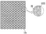
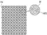
도 2는 본 발명의 실시예에 의한 터치 스크린 패널을 개략적으로 도시한 평면도이다. 그리고, 도 3a는 도 2에 도시된 제1 감지패턴들 및 제1 더미패턴들의 일례를 도시한 평면도이고, 도 3b는 도 2에 도시된 제2 감지패턴들 및 제2 더미패턴들의 일례를 도시한 평면도이다.2 is a plan view schematically illustrating a touch screen panel according to an exemplary embodiment of the present invention. 3A is a plan view illustrating an example of the first sensing patterns and the first dummy patterns illustrated in FIG. 2, and FIG. 3B illustrates an example of the second sensing patterns and the second dummy patterns illustrated in FIG. 2. One floor plan.
도 2 내지 도 3b를 참조하면, 본 발명의 실시예에 의한 터치 스크린 패널(10)은 서로 어긋나도록 교호적으로 배치되며 다이아몬드 패턴과 같이 규칙적인 패턴으로 밀접되도록 형성된 다수의 제1 및 제2 감지패턴들(12, 14)과, 제1 및 제2 감지패턴들(12, 14)을 위치 검출라인(15_1)과 전기적으로 연결하는 다수의 금속패턴들(15)을 포함한다. 그리고, 제1 감지패턴들(12) 사이의 더미영역과 제2 감지패턴들(14) 사이의 더미영역에는 각각 다수의 제1 및 제2 더미패턴들(DX, DY)이 형성된다.2 to 3B, the
제1 감지패턴들(12)은 투명전극물질로 형성되며, 제1 방향을 따라 연결되도록 패터닝된 다수의 패턴들을 포함한다. 여기서, 제1 방향은 매트릭스 상의 열방향 또는 행방향 등이 될 수 있으며, 편의상 이하에서 제1 방향은 열방향이라 가정하여 설명하기로 한다. 예를 들어, 제1 감지패턴들(12)은 X 좌표가 동일한 하나의 열 단위의 패턴들끼리 서로 연결되도록 패터닝된 다수의 X 패턴들로 구현될 수 있다.The
이와 같은 제1 감지패턴들(12)은 열 단위로 제1 패드부(12a)를 구비하며, 제1 패드부(12a)를 통해 연결되는 금속패턴들(15)에 의해 열 단위로 위치 검출라인(15_1)과 연결된다.The
그리고, 제1 감지패턴들(12) 사이의 더미영역에는 제2 감지패턴들(14)과 대응되도록(예컨대, 중첩되도록) 다수의 제1 더미패턴들(DX)이 형성된다. 제1 더미패턴들(DX)은 각각이 분리된 패턴을 갖도록 형성되며, 위치 검출라인(15_1)과 연결되지는 않는다.In addition, a plurality of first dummy patterns DX is formed in the dummy region between the
이와 같은 제1 더미패턴들(DX)은 제1 감지패턴들(12)과 동일한 투명전극물질로 형성될 수 있다. 즉, 제1 더미패턴들(DX)은 제1 감지패턴들(12)이 형성되는 공정단계에서, 제1 감지패턴들(12)과 함께 패터닝되어 형성될 수 있다.The first dummy patterns DX may be formed of the same transparent electrode material as the
제2 감지패턴들(14)은 투명전극물질로 형성되며, 제2 방향을 따라 연결되도록 패터닝된 다수의 패턴들을 포함한다. 여기서, 제2 방향은 제1 방향과 교차하는 방향이다. 예컨대, 제1 방향이 열방향으로 설정되면, 제2 방향은 행방향으로 설정될 수 있다.The
이 경우, 제2 감지패턴들(14)은 Y 좌표가 동일한 하나의 행 단위의 패턴들끼리 서로 연결되도록 패터닝된 다수의 Y 패턴들로 구현될 수 있다.In this case, the
이와 같은 제2 감지패턴들(14)은 행 단위로 제2 패드부(14a)를 구비하며, 제2 패드부(14a)를 통해 연결되는 금속패턴들(15)에 의해 행 단위로 위치 검출라인(15_1)과 연결된다.The
그리고, 제2 감지패턴들(14) 사이의 더미영역에는 제1 감지패턴들(12)과 대응되도록(예컨대, 중첩되도록) 다수의 제2 더미패턴들(DY)이 형성된다. 제2 더미패 턴들(DY)은 각각이 분리된 패턴을 갖도록 형성되며, 위치 검출라인(15_1)과 연결되지는 않는다.In addition, a plurality of second dummy patterns DY are formed in the dummy region between the
이와 같은 제2 더미패턴들(DY)은 제2 감지패턴들(14)과 동일한 투명전극물질로 형성될 수 있다. 즉, 제2 더미패턴들(DY)은 제2 감지패턴들(14)이 형성되는 공정단계에서, 제2 감지패턴들(14)과 함께 패터닝되어 형성될 수 있다.The second dummy patterns DY may be formed of the same transparent electrode material as the
금속패턴들(15)은 제1 및 제2 감지패턴들(12, 14)이 위치되는 영역의 가장자리에서 제1 및 제2 감지패턴들의 제1, 2 패드부(12a, 14a)와 전기적으로 연결되어, 제1 및 제2 감지패턴들(12, 14)을 위치 검출라인(15_1)과 전기적으로 연결한다.The
예컨대, 금속패턴들(15)은, 하나의 열 단위의 제1 감지패턴들(12)을 각각의 위치 검출라인(15_1)과 전기적으로 연결함과 아울러, 하나의 행 단위의 제2 감지패턴들(14)을 각각의 위치 검출라인(15_1)과 전기적으로 연결할 수 있다.For example, the
위치 검출라인(15_1)은 금속패턴들(15)을 통해 제1 및 제2 감지패턴들(12, 14)과 연결되어 이들을 구동회로(미도시)와 연결한다. 예컨대, 터치 스크린 패널(10)이 패드부(20)를 통해 외부의 구동회로와 연결되는 경우, 위치 검출라인(15_1)은 패드부(20)와 감지패턴들(12, 14) 사이에 연결될 수 있다.The position detection line 15_1 is connected to the first and
한편, 앞선 설명에서, 금속패턴들(15)과 위치 검출라인(15_1)을 별도의 구성요소로 분리하여 설명하였지만, 이들은 동일한 공정 단계에서 동일 재료로 일체화되어 형성될 수도 있음은 물론이다.Meanwhile, in the above description, the
전술한 바와 같은 터치 스크린 패널(10)은 정전용량성 터치 스크린 패널로, 사람의 손 또는 터치스틱 등과 같은 접촉물체가 접촉되면, 감지패턴들(12, 14)로부 터 금속패턴들(15), 위치 검출라인(15_1) 및 패드부(20)를 경유하여 구동회로 측으로 접촉위치에 따른 정전용량의 변화가 전달된다. 그리고, X 및 Y 입력처리회로(미도시) 등에 의해 정전용량의 변화가 전기적 신호로 변환됨에 의해 접촉위치가 파악된다.As described above, the
단, 본 발명에서, 제1 감지패턴들(12)과 제2 감지패턴들(14)은 서로 다른 기판에 형성되어 서로 다른 레이어에 배치된다. 이 경우, 패터닝 단계에서부터 제1 감지패턴들(12)이 제1 방향으로 서로 연결되도록 패터닝하고, 제2 감지패턴들(14)이 제2 방향으로 서로 연결되도록 패터닝할 수 있다. 따라서, 별도의 컨택홀 및 연결패턴들을 형성하는 과정을 생략할 수 있어, 마스크 수가 저감되고 공정이 단순화된다.However, in the present invention, the
또한, 제1 감지패턴들(12)과 제2 감지패턴들(14)이 서로 다른 기판에 구비됨에 따라, 이들 사이의 이격거리가 충분히 확보되어 절연특성을 향상시킬 수 있다. 특히, 제1 감지패턴들(12)이 형성된 기판과 제2 감지패턴들(14)이 형성된 기판사이에 절연층을 구비하는 경우, 이들 사이의 절연특성을 보다 향상시킬 수 있다.In addition, as the
또한, 본 발명에서는 제1 감지패턴들(12)의 사이 및 제2 감지패턴들(14)의 사이에 각각 제1 더미패턴들(DX) 및 제2 더미패턴들(DY)을 형성함에 의하여, 제1 및 제2 감지패턴들(12, 14)이 서로 다른 기판의 상이한 레이어에 배치됨에 따른 감지패턴들의 반사율차를 개선할 수 있다.Further, in the present invention, by forming the first dummy patterns DX and the second dummy patterns DY between the
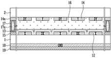
도 4는 도 2에 도시된 터치 스크린 패널의 요부 결합단면도이다. 도 4를 설 명할 때, 도 2 내지 도 3b와 동일한 부분에 대해서는 동일 부호를 부여하고, 이에 대한 상세한 설명은 생략하기로 한다. 또한, 편의상 도 4에서는 제1 및 제2 감지패턴들의 연결부는 도시하지 않기로 한다.4 is a cross-sectional view illustrating main parts of the touch screen panel illustrated in FIG. 2. 4, the same parts as in FIGS. 2 to 3B are denoted by the same reference numerals, and detailed description thereof will be omitted. Also, for convenience, the connecting portion of the first and second sensing patterns is not shown in FIG. 4.
도 4를 참조하면, 터치 스크린 패널(10)은 서로 대향되도록 배치되며 실링제(17)에 의해 합착되는 제1 및 제2 기판(1, 2)을 구비한다. 여기서, 제1 및 제2 기판(1, 2)은 터치 스크린 패널(10)의 상,하부 기판으로, 상부기판은 윈도우와 일체화되어 구현될 수 있다.Referring to FIG. 4, the
편의상, 이하에서는 제1 기판(1)을 하부기판이라 가정하고, 제2 기판(2)은 상부기판이라 가정하기로 한다. 하지만, 제1 기판(1)이 상부기판이 되고, 제2 기판(2)이 하부기판이 될 수도 있음은 물론이다.For convenience, hereinafter, it is assumed that the
제1 기판(1)의 상부면, 즉 제2 기판(2)을 향하는 일면에는, 제1 방향을 따라 연결되는 다수의 제1 감지패턴들(12)과, 제1 감지패턴들(12)의 사이에 제2 감지패턴들(14)과 대응되도록 형성되는 다수의 제1 더미패턴들(DX)과, 금속패턴들(15)이 형성된다. 또한, 도 4에는 도시되지 않았으나, 제1 기판(1)의 일면에는 도 2에 도시된 위치 검출라인(15_1)과 터치 스크린 패널의 패드부(20) 등이 더 형성될 수 있다.An upper surface of the
한편, 제1 기판(1)의 하부면, 즉 표시패널(미도시)을 향하는 타면에는, 투명접지전극(18)과, 투명 접지전극(18)을 커버하는 절연막(19)이 더 형성될 수 있다.The
투명 접지전극(17)은 터치 스크린 패널(10)과 표시패널 등의 사이에서 안정성을 확보하는데 이용될 수 있고, 터치 스크린 패널(10)의 설계 방식에 따라서는 제1 및 제2 감지패턴들(12, 14)과 정전용량을 형성하는 데에도 이용될 수 있다. 이와 같은 투명 접지전극(18) 및/또는 절연막(19)은 제품 설계에 따라 생략되는 것도 가능하다.The
제2 기판(2)의 하부면, 즉 제1 기판(1)을 향하는 일면에는, 제2 방향을 따라 연결되되 제1 감지패턴들(12)과 중첩되지 않도록 배치되는 다수의 제2 감지패턴들(14)과, 제2 감지패턴들(14)의 사이에 제1 감지패턴들(12)과 대응되도록 형성되는 다수의 제2 더미패턴들(DY)이 형성된다.On the lower surface of the
여기서, 제2 감지패턴들의 제2 패드부(14a)는 실링제(17)를 통하여 금속패턴들(15)과 전기적으로 연결된다. 이를 위해, 실링제(17)는 도전볼(17a)과 같은 도전성물질을 함유하며, 적어도 제2 감지패턴들의 제2 패드부(14a)와 금속패턴들(15) 사이에 배치될 수 있다.Here, the
한편, 제1 감지패턴들(12)이 금속패턴들(15)이 형성되는 기판과 상이한 기판에 형성되는 경우에는, 실링제(17)가 제1 감지패턴들의 패드부(12a)와 금속패턴들(15)을 전기적으로 연결하도록 배치될 수도 있다.On the other hand, when the
실링제(17)에 의해 합착된 제1 기판(1)과 제2 기판(2) 사이의 공간에는 절연층이 개재된다.An insulating layer is interposed in the space between the
예컨대, 절연층은 제1 감지패턴들(12) 및 제1 더미패턴들(DX)을 커버하도록 제1 기판(1) 상에 형성된 제1 절연막(13)을 포함할 수 있다. 또한, 도시되지는 않았으나, 절연층은 제2 감지패턴들(14) 및 제2 더미패턴들(DY)을 커버하도록 제2 기판(2) 상에 형성된 제2 절연막을 포함할 수도 있다. 단, 제1 절연막(13) 및 제2 절 연막은 선택적으로 구비될 수 있는 것으로, 어느 하나, 혹은 둘다 구비되거나 혹은 모두 구비되지 않을 수도 있다.For example, the insulating layer may include a first insulating
또한, 절연층은 제1 감지패턴들(12) 및 제1 더미패턴들(DX)이 형성된 제1 기판(1)과, 제2 감지패턴들(14) 및 제2 더미패턴들(DY)이 형성된 제2 기판(2) 사이의 공간에 채워진 충전제 물질(16)을 포함할 수 있다.In addition, the insulating layer may include the
여기서, 충전제 물질(16)은 터치 스크린 패널(10)에서의 광손실을 최소화하기 위하여 제1 및 제2 기판(1, 2)의 굴절률과 공기의 굴절률 사이의 굴절률을 갖는 물질로 형성될 수 있다. 예컨대, 충전제 물질(16)은 제1 및 제2 기판(1, 2)이 유리(glass)로 형성되는 경우, 유리와 유사한 굴절률을 갖는 SVR(Super View Resin)로 형성될 수 있다.Here, the
이와 같은 충전제 물질(16)은 주입방식, 혹은, 적하방식을 통해 제1 기판(1)과 제2 기판(2) 사이에 채워질 수 있다.The
전술한 바와 같은 본 발명의 터치 스크린 패널(10)은 제1 감지패턴들(12)과 제2 감지패턴들(14)을 서로 다른 기판에 형성함과 아울러 제1 기판(1)과 제2 기판(2) 사이에 충전제 물질(16) 등을 포함하는 절연층을 구비한다.As described above, the
이에 의해, 제1 또는 제2 감지패턴들(12, 14)을 연결하기 위한 별도의 연결패턴을 형성할 필요가 없어져 마스크 수가 저감되고 공정이 단순화된다.As a result, it is not necessary to form a separate connection pattern for connecting the first or
또한, 제1 감지패턴들(12)과 제2 감지패턴들(14) 사이에 절연층이 개재됨은 물론, 이들이 각기 다른 기판에 형성되기 때문에 제1 감지패턴들(12)과 제2 감지패턴들(14) 사이의 거리가 충분히 확보된다. 이에 따라, 제1 감지패턴들(12)과 제2 감지패턴들(14) 사이에 충분한 절연특성을 확보할 수 있다.In addition, since the insulating layer is interposed between the
또한, 본 발명의 터치 스크린 패널(10)은 제1 감지패턴들(12)의 사이에 제2 감지패턴들(14)과 대응되도록 형성된 제1 더미패턴들(DX)과, 제2 감지패턴들(14)의 사이에 제1 감지패턴들(12)과 대응되도록 형성된 제2 더미패턴들(DY)을 구비한다.In addition, the
이에 의해, 제1 감지패턴들(12)이 형성되는 레이어와 제2 감지패턴들(14)이 형성되는 레이어가 서로 대응되는 유사 패턴을 포함하게 된다. 따라서, 터치 스크린 패널(10)의 터치영역(제1 및 제2 감지패턴들(12, 14)이 형성되는 광투과영역) 전반적으로, 반사율이 균일해지게 된다.As a result, the layer on which the
도 5a 내지 도 5d는 주입방식을 통해 도 4에 도시된 터치 스크린 패널을 제조하는 방법을 순차적으로 도시한 단면도이다.5A through 5D are cross-sectional views sequentially illustrating a method of manufacturing the touch screen panel shown in FIG. 4 through an injection method.
도 5a 내지 도 5d를 참조하면, 우선, 도 5a에 도시된 바와 같이, 제1 감지패턴들(12), 제1 더미패턴들(DX) 및 금속패턴들(15) 등이 구비된 제1 기판(1)과, 제2 감지패턴들(14) 및 제2 더미패턴들(DY) 등이 구비된 제2 기판(2)을 준비한 후, 제1 기판(1)과 제2 기판(2)을 정렬한다.5A through 5D, first, as shown in FIG. 5A, a first substrate including
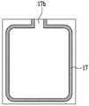
이때, 제1 기판(1) 또는 제2 기판(2)의 외곽에는 도 7a에 도시된 바와 같이 주입구(17b)가 구비되는 형상으로 실링제(17)가 형성된다.At this time, the sealing
이후, 도 5b에 도시된 바와 같이, 제1 기판(1)과 제2 기판(2)을 조립한 후, 실링제(17)에 의해 제1 기판(1)과 제2 기판(2)을 합착한다.Thereafter, as shown in FIG. 5B, after assembling the
이후, 도 5c에 도시된 바와 같이, 주입기(30)를 이용하여 SVR 등의 충전제 물질(16)을 제1 기판(1)과 제2 기판(2) 사이에 주입한다.Subsequently, as shown in FIG. 5C, a
이후, 도 5d에 도시된 바와 같이, 제1 기판(1)과 제2 기판(2) 사이에 충전제 물질(16)이 채워지면, 주입구를 봉한다.Thereafter, as shown in FIG. 5D, when the
전술한 바와 같은 주입방식을 통해 터치 스크린 패널을 제조하면, 제1 및 제2 기판(1, 2) 사이에 충전제 물질(16)을 채우는 과정에서 기포(air bubble) 발생과 이물 유입을 최소화할 수 있다.When the touch screen panel is manufactured through the injection method as described above, air bubble generation and foreign material inflow can be minimized while filling the
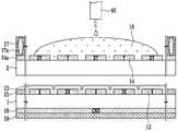
도 6a 내지 도 6c는 적하방식을 통해 도 4에 도시된 터치 스크린 패널을 제조하는 방법을 순차적으로 도시한 단면도이다.6A through 6C are cross-sectional views sequentially illustrating a method of manufacturing the touch screen panel shown in FIG. 4 through a dropping method.
도 6a 내지 도 6c를 참조하면, 우선, 도 6a에 도시된 바와 같이, 제1 감지패턴들(12), 제1 더미패턴들(DX) 및 금속패턴들(15) 등이 구비된 제1 기판(1)과, 제2 감지패턴들(14) 및 제2 더미패턴들(DY) 등이 구비된 제2 기판(2)을 준비한다.6A through 6C, first, as illustrated in FIG. 6A, a first substrate including
이때, 제1 기판(1) 또는 제2 기판(2)의 외곽에는 도 7b에 도시된 바와 같이 실링제(17)가 형성된다. 편의상, 본 실시예에서 실링제(17)는 제2 기판(2)에 형성되는 것으로 가정하기로 한다. 이 경우, 제2 기판(2)의 내측면에는 적하기(40)에 의해 충전제 물질(16)이 적하되어 채워진다.At this time, the sealing
이후, 도 6b에 도시된 바와 같이, 제1 기판(1) 및 제2 기판(2)을 정렬하고, 충전제 물질(16)이 채워진 제2 기판(2)의 내측면이 제1 기판(1) 방향의 하부방향을 향하도록 하면서 제1 기판(1) 및 제2 기판(2)을 조립한다.Thereafter, as shown in FIG. 6B, the
이후, 도 6c에 도시된 바와 같이, 실링제(17)에 의해 제1 기판(1)과 제2 기 판(2)을 합착한다.Thereafter, as shown in FIG. 6C, the
단, 전술한 바와 같은 적하방식에 의해 제1 및 제2 기판(1, 2) 사이에 충전제 물질(16)을 채울 때에는 진공하에서 공정이 진행되도록 한다. 즉, 본 실시예에서는 진공 적하방식을 통해 터치 스크린 패널을 제조한다.However, when the
이와 같이, 진공 적하방식을 통해 터치 스크린 패널을 제조하면, 제1 및 제2 기판(1, 2) 사이에 충전제 물질(16)을 채우는 과정에서 기포(air bubble) 발생과 이물 유입을 최소화할 수 있다.As such, when the touch screen panel is manufactured by vacuum dropping, air bubbles and foreign matters may be minimized while filling the
본 발명의 기술 사상은 상기 바람직한 실시예에 따라 구체적으로 기술되었으나, 상기한 실시예는 그 설명을 위한 것이며 그 제한을 위한 것이 아님을 주의하여야 한다. 또한, 본 발명의 기술 분야의 통상의 지식을 가진 자라면 본 발명의 기술 사상의 범위 내에서 다양한 변형예가 가능함을 이해할 수 있을 것이다.While the present invention has been particularly shown and described with reference to exemplary embodiments thereof, it is to be understood that the invention is not limited to the disclosed exemplary embodiments. It will be apparent to those skilled in the art that various modifications may be made without departing from the scope of the present invention.
도 1은 본 발명의 실시예에 의한 감지패턴들의 배치를 나타낸 평면도이다.1 is a plan view illustrating an arrangement of sensing patterns according to an exemplary embodiment of the present invention.
도 2는 본 발명의 실시예에 의한 터치 스크린 패널을 개략적으로 도시한 평면도이다.2 is a plan view schematically illustrating a touch screen panel according to an exemplary embodiment of the present invention.
도 3a는 도 2에 도시된 제1 감지패턴들 및 제1 더미패턴들의 일례를 도시한 평면도이다.3A is a plan view illustrating an example of the first sensing patterns and the first dummy patterns shown in FIG. 2.
도 3b는 도 2에 도시된 제2 감지패턴들 및 제2 더미패턴들의 일례를 도시한 평면도이다.3B is a plan view illustrating an example of the second sensing patterns and the second dummy patterns shown in FIG. 2.
도 4는 도 2에 도시된 터치 스크린 패널의 요부 결합단면도이다.4 is a cross-sectional view illustrating main parts of the touch screen panel illustrated in FIG. 2.
도 5a 내지 도 5d는 주입방식을 통해 도 4에 도시된 터치 스크린 패널을 제조하는 방법을 순차적으로 도시한 단면도이다.5A through 5D are cross-sectional views sequentially illustrating a method of manufacturing the touch screen panel shown in FIG. 4 through an injection method.
도 6a 내지 도 6c는 적하방식을 통해 도 4에 도시된 터치 스크린 패널을 제조하는 방법을 순차적으로 도시한 단면도이다.6A through 6C are cross-sectional views sequentially illustrating a method of manufacturing the touch screen panel shown in FIG. 4 through a dropping method.
도 7a는 주입방식에 의한 실링제의 형상을 도시한 평면도이다.7A is a plan view showing the shape of the sealing agent by the injection method.
도 7b는 적하방식에 의한 실링제의 형상을 도시한 평면도이다.7B is a plan view showing the shape of the sealing agent by the dropping method.
<도면의 주요 부분에 대한 부호의 설명><Explanation of symbols for the main parts of the drawings>
10: 터치 스크린 패널1, 2: 기판10:
12, 14: 감지패턴16: 충전제 물질12, 14: detection pattern 16: filler material
17: 실링제DX, DY: 더미패턴17: sealing agent DX, DY: dummy pattern
Claims (13)
Translated fromKoreanPriority Applications (5)
| Application Number | Priority Date | Filing Date | Title |
|---|---|---|---|
| KR1020090003635AKR101048980B1 (en) | 2009-01-16 | 2009-01-16 | Touch screen panel and its manufacturing method |
| JP2009165811AJP2010165336A (en) | 2009-01-16 | 2009-07-14 | Touch screen panel and method for manufacturing the same |
| US12/543,421US8847893B2 (en) | 2009-01-16 | 2009-08-18 | Touch screen panel and method of fabricating the same |
| CN200910209382.8ACN101782819B (en) | 2009-01-16 | 2009-11-04 | Touch screen panel and fabricating method for the same |
| EP09176884.6AEP2209063B1 (en) | 2009-01-16 | 2009-11-24 | Touch screen panel and method of fabricating the same |
Applications Claiming Priority (1)
| Application Number | Priority Date | Filing Date | Title |
|---|---|---|---|
| KR1020090003635AKR101048980B1 (en) | 2009-01-16 | 2009-01-16 | Touch screen panel and its manufacturing method |
Publications (2)
| Publication Number | Publication Date |
|---|---|
| KR20100084255A KR20100084255A (en) | 2010-07-26 |
| KR101048980B1true KR101048980B1 (en) | 2011-07-12 |
Family
ID=42034683
Family Applications (1)
| Application Number | Title | Priority Date | Filing Date |
|---|---|---|---|
| KR1020090003635AActiveKR101048980B1 (en) | 2009-01-16 | 2009-01-16 | Touch screen panel and its manufacturing method |
Country Status (5)
| Country | Link |
|---|---|
| US (1) | US8847893B2 (en) |
| EP (1) | EP2209063B1 (en) |
| JP (1) | JP2010165336A (en) |
| KR (1) | KR101048980B1 (en) |
| CN (1) | CN101782819B (en) |
Families Citing this family (55)
| Publication number | Priority date | Publication date | Assignee | Title |
|---|---|---|---|---|
| JP5591834B2 (en) | 2009-03-04 | 2014-09-17 | ナム、ドンシク | Touch panel sensor |
| US9753597B2 (en) | 2009-07-24 | 2017-09-05 | Cypress Semiconductor Corporation | Mutual capacitance sensing array |
| TWM380534U (en)* | 2009-11-05 | 2010-05-11 | Transtouch Technology Inc | Capacitive touch panel |
| JP2011154442A (en)* | 2010-01-26 | 2011-08-11 | Sony Corp | Sensor element and display apparatus |
| US8970508B2 (en)* | 2010-02-11 | 2015-03-03 | Lg Display Co., Ltd. | Touch screen panel |
| WO2011102168A1 (en)* | 2010-02-17 | 2011-08-25 | 日本写真印刷株式会社 | Transparent electrode film |
| KR101113471B1 (en) | 2010-04-01 | 2012-02-29 | 삼성모바일디스플레이주식회사 | Touch Screen Panel |
| KR101056264B1 (en)* | 2010-05-14 | 2011-08-11 | 삼성모바일디스플레이주식회사 | Touch screen panel |
| JP5475190B2 (en)* | 2010-06-16 | 2014-04-16 | サムウォン エスティー | Touch panel sensor |
| KR101669538B1 (en)* | 2010-08-11 | 2016-10-28 | 삼성디스플레이 주식회사 | Touch Screen Panel and Fabricating Method Thereof |
| KR101691619B1 (en)* | 2010-09-14 | 2017-01-02 | 삼성디스플레이 주식회사 | Touch Screen Panel and Display Device Having the Same |
| US8638307B2 (en)* | 2010-09-27 | 2014-01-28 | Blackberry Limited | Electronic device and touch-sensitive input device |
| KR101704536B1 (en)* | 2010-10-08 | 2017-02-09 | 삼성전자주식회사 | Touch Panel type of Slim and Portable Device including the same |
| KR101224419B1 (en)* | 2010-10-26 | 2013-01-22 | (주)삼원에스티 | Touch panel sensor |
| KR20120065687A (en)* | 2010-12-13 | 2012-06-21 | 삼성모바일디스플레이주식회사 | Touch screen panel |
| KR101734555B1 (en)* | 2011-01-03 | 2017-05-11 | 엘지이노텍 주식회사 | Method for manufacturing touch panel |
| KR101793677B1 (en)* | 2011-01-18 | 2017-11-06 | 삼성디스플레이 주식회사 | Touch Screen Panel |
| US8558807B2 (en)* | 2011-02-15 | 2013-10-15 | Teh-Zheng Lin | Transparent touch panel |
| JP5496143B2 (en)* | 2011-04-04 | 2014-05-21 | 信越ポリマー株式会社 | Capacitance sensor sheet and manufacturing method thereof |
| KR101303635B1 (en)* | 2011-05-26 | 2013-09-11 | 엘지이노텍 주식회사 | Touch window |
| TWI459269B (en)* | 2011-06-07 | 2014-11-01 | Rtr Tech Technology Co Ltd | Manufacturing method of touch panel |
| EP2538313B1 (en)* | 2011-06-20 | 2015-05-20 | Melfas, Inc. | Touch sensor panel |
| CN103649883B (en)* | 2011-07-11 | 2017-09-08 | 富士胶片株式会社 | Conducting strip and its manufacture method, touch-screen and display device |
| JP5734243B2 (en)* | 2011-07-11 | 2015-06-17 | 富士フイルム株式会社 | Conductive sheet, touch panel and display device |
| JP5808966B2 (en)* | 2011-07-11 | 2015-11-10 | 富士フイルム株式会社 | Conductive laminate, touch panel and display device |
| JP5806559B2 (en)* | 2011-09-06 | 2015-11-10 | 富士フイルム株式会社 | Conductive sheet, touch panel and display device |
| WO2013012428A1 (en)* | 2011-07-15 | 2013-01-24 | Cypress Semiconductor Corporaton | Capacitance sensing circuits, methods and systems having ground insertion electrodes |
| JP5781886B2 (en)* | 2011-10-05 | 2015-09-24 | 富士フイルム株式会社 | Conductive sheet, touch panel and display device |
| US20130093697A1 (en)* | 2011-10-18 | 2013-04-18 | Wei-Hao Sun | Touch panel display and assembly process thereof |
| TWI531936B (en)* | 2011-10-24 | 2016-05-01 | 友達光電股份有限公司 | Touch display device |
| KR101421706B1 (en)* | 2011-11-16 | 2014-07-24 | (주) 태양기전 | Touch screen panel and manufacturing method of the same |
| US9323092B2 (en) | 2011-12-05 | 2016-04-26 | Htc Corporation | Touch panel |
| CN103135831B (en)* | 2011-12-05 | 2016-03-30 | 宏达国际电子股份有限公司 | touch panel |
| CN103197784B (en)* | 2012-01-06 | 2016-05-25 | 宸鸿科技(厦门)有限公司 | Contact panel and preparation method thereof |
| JP5942454B2 (en)* | 2012-02-08 | 2016-06-29 | 大日本印刷株式会社 | Touch panel sensor, display device with touch panel, and method of manufacturing touch panel sensor |
| WO2013129810A1 (en)* | 2012-02-29 | 2013-09-06 | 미래나노텍 주식회사 | Touch screen sensor, image display device having same, and manufacturing method therefor |
| KR101975536B1 (en)* | 2012-07-30 | 2019-05-08 | 삼성디스플레이 주식회사 | flexible touch screen panel |
| KR102024783B1 (en)* | 2012-11-16 | 2019-09-25 | 엘지디스플레이 주식회사 | Touch screen panel for display device |
| JP6040317B2 (en)* | 2012-11-30 | 2016-12-07 | エルジー・ケム・リミテッド | Touch screen and manufacturing method thereof |
| WO2014133347A1 (en)* | 2013-02-27 | 2014-09-04 | 미래나노텍 주식회사 | Structure of touch pad using dummy pattern for capacitive type touch screen |
| JP6674257B2 (en)* | 2013-02-27 | 2020-04-01 | ミラエナノテック カンパニー リミテッド | Structure of Touchpad Using Dummy Pattern for Capacitive Touch Screen |
| KR101447805B1 (en)* | 2013-02-28 | 2014-10-07 | 희성전자 주식회사 | Touch screen panel |
| EP2957996A4 (en)* | 2013-03-22 | 2016-11-02 | Lg Chemical Ltd | Conductive pattern laminate and electronic device comprising same |
| US20140300831A1 (en)* | 2013-04-08 | 2014-10-09 | Young Fast Optoelectronics Co., Ltd. | Transparent capacitive touch panel |
| US9298300B2 (en)* | 2013-05-01 | 2016-03-29 | Apple Inc. | Displays with integrated touch and improved image pixel aperture |
| KR102091035B1 (en)* | 2013-09-03 | 2020-03-20 | 엘지디스플레이 주식회사 | Display device having touch screen |
| KR102271114B1 (en)* | 2014-03-28 | 2021-06-30 | 삼성디스플레이 주식회사 | Touch sensing panel |
| TWI486862B (en)* | 2014-05-06 | 2015-06-01 | Apex Material Technology Corp | Capacitive touch circuit and touch sensor and capacitive touch system using the same |
| US10048788B2 (en) | 2015-03-09 | 2018-08-14 | Apple Inc. | Touch screen display uniformity |
| KR102320640B1 (en)* | 2015-04-29 | 2021-11-02 | 삼성디스플레이 주식회사 | Display apparatus and manufacturing method thereof |
| CN106299148B (en)* | 2015-06-10 | 2018-04-03 | 上海和辉光电有限公司 | The encapsulating structure and method for packing of display panel |
| KR102592972B1 (en)* | 2016-02-12 | 2023-10-24 | 삼성전자주식회사 | Sensing Module substrate and Sensing Module including the same |
| MX381491B (en)* | 2016-04-13 | 2025-03-12 | Tactotek Oy | Multilayer structure with embedded multilayer electronics |
| KR102283011B1 (en)* | 2017-03-15 | 2021-07-29 | 삼성디스플레이 주식회사 | Touch sensor, display device having the same and fabricating method of display device |
| KR102620293B1 (en)* | 2021-04-26 | 2024-01-03 | 엘지이노텍 주식회사 | Printed circuit board and Electronic parts having the same |
Citations (3)
| Publication number | Priority date | Publication date | Assignee | Title |
|---|---|---|---|---|
| KR20010034828A (en)* | 1998-04-24 | 2001-04-25 | 니폰샤신인사츠가부시키가이샤 | Touch panel device |
| KR20050072680A (en)* | 2004-01-07 | 2005-07-12 | 엘란 마이크로일렉트로닉스 코포레이션 | Capacitive touchpad and method for forming the same |
| JP2008129708A (en)* | 2006-11-17 | 2008-06-05 | Alps Electric Co Ltd | Transparent touch panel and its manufacturing method |
Family Cites Families (32)
| Publication number | Priority date | Publication date | Assignee | Title |
|---|---|---|---|---|
| JPH0614157B2 (en)* | 1983-12-27 | 1994-02-23 | セイコーエプソン株式会社 | Liquid cell |
| US4760003A (en)* | 1985-05-24 | 1988-07-26 | Canon Kabushiki Kaisha | Electrophotographic photosensitive member containing disazo compound |
| JPS63174120A (en)* | 1987-01-14 | 1988-07-18 | Fujitsu Ltd | capacitive touch panel |
| JPS6441022A (en)* | 1987-08-05 | 1989-02-13 | Fujitsu Ltd | Panel structure for coordinate detector |
| US5392058A (en)* | 1991-05-15 | 1995-02-21 | Sharp Kabushiki Kaisha | Display-integrated type tablet device |
| JPH08272532A (en)* | 1995-02-01 | 1996-10-18 | Alps Electric Co Ltd | Display device with tablet |
| JP3220403B2 (en)* | 1996-02-09 | 2001-10-22 | セイコーインスツルメンツ株式会社 | Display device manufacturing method |
| US6204896B1 (en)* | 1996-02-09 | 2001-03-20 | Seiko Instruments Inc. | Display unit, manufacturing method thereof and electronic device equipped with same |
| US6188391B1 (en)* | 1998-07-09 | 2001-02-13 | Synaptics, Inc. | Two-layer capacitive touchpad and method of making same |
| JP2000029612A (en)* | 1998-07-15 | 2000-01-28 | Smk Corp | Touch panel input device |
| US6872933B2 (en)* | 1998-07-15 | 2005-03-29 | Alvin R. Wirthlin | Optical transducer |
| EP1230248B1 (en)* | 1999-11-15 | 2007-06-06 | Therasense, Inc. | Transition metal complexes attached to a polymer via a flexible chain |
| JP2003099185A (en)* | 2001-09-20 | 2003-04-04 | Alps Electric Co Ltd | Input device |
| US7154481B2 (en) | 2002-06-25 | 2006-12-26 | 3M Innovative Properties Company | Touch sensor |
| US7936338B2 (en) | 2002-10-01 | 2011-05-03 | Sony Corporation | Display unit and its manufacturing method |
| JP4136586B2 (en)* | 2002-10-11 | 2008-08-20 | 富士通コンポーネント株式会社 | Touch panel |
| KR20070017296A (en) | 2003-10-15 | 2007-02-09 | 쓰리엠 이노베이티브 프로퍼티즈 컴파니 | Patterned conductor touch screen with improved optical properties |
| JP2006065611A (en)* | 2004-08-27 | 2006-03-09 | Matsushita Electric Ind Co Ltd | Input device and input system using the same |
| KR100703542B1 (en) | 2005-05-02 | 2007-04-03 | 삼성에스디아이 주식회사 | Light emitting display device with touch panel |
| EP1892609A4 (en)* | 2005-05-26 | 2013-03-27 | Gunze Kk | Transparent planar body and transparent touch switch |
| TWI267773B (en)* | 2005-05-31 | 2006-12-01 | Wintek Corp | Manufacturing method of a touch panel |
| US7932898B2 (en)* | 2005-09-20 | 2011-04-26 | Atmel Corporation | Touch sensitive screen |
| US8169421B2 (en)* | 2006-06-19 | 2012-05-01 | Cypress Semiconductor Corporation | Apparatus and method for detecting a touch-sensor pad gesture |
| US20080088595A1 (en)* | 2006-10-12 | 2008-04-17 | Hua Liu | Interconnected two-substrate layer touchpad capacitive sensing device |
| US8120584B2 (en)* | 2006-12-21 | 2012-02-21 | Cypress Semiconductor Corporation | Feedback mechanism for user detection of reference location on a sensing device |
| US20100073316A1 (en)* | 2007-03-27 | 2010-03-25 | Junichi Nozawa | Touch panel and display apparatus with touch panel |
| US20080309633A1 (en)* | 2007-06-13 | 2008-12-18 | Apple Inc. | Touch-sensitive display |
| JP2009009249A (en)* | 2007-06-26 | 2009-01-15 | Nissha Printing Co Ltd | Capacitance type touch panel and two system combined use touch panel using the same |
| TWI367437B (en)* | 2007-09-29 | 2012-07-01 | Au Optronics Corp | Touch panel and manufacturing method thereof |
| TW200919287A (en)* | 2007-10-17 | 2009-05-01 | Wintek Corp | Touch panel and manufacturing method thereof |
| US20100045625A1 (en)* | 2008-08-21 | 2010-02-25 | Tpo Displays Corp. | Touch panel and system for displaying images utilizing the same |
| CA2742985A1 (en) | 2008-11-06 | 2010-05-14 | Uico, Inc. | Capacitive touch screen and strategic geometry isolation patterning method for making touch screens |
- 2009
- 2009-01-16KRKR1020090003635Apatent/KR101048980B1/enactiveActive
- 2009-07-14JPJP2009165811Apatent/JP2010165336A/enactivePending
- 2009-08-18USUS12/543,421patent/US8847893B2/enactiveActive
- 2009-11-04CNCN200910209382.8Apatent/CN101782819B/enactiveActive
- 2009-11-24EPEP09176884.6Apatent/EP2209063B1/enactiveActive
Patent Citations (3)
| Publication number | Priority date | Publication date | Assignee | Title |
|---|---|---|---|---|
| KR20010034828A (en)* | 1998-04-24 | 2001-04-25 | 니폰샤신인사츠가부시키가이샤 | Touch panel device |
| KR20050072680A (en)* | 2004-01-07 | 2005-07-12 | 엘란 마이크로일렉트로닉스 코포레이션 | Capacitive touchpad and method for forming the same |
| JP2008129708A (en)* | 2006-11-17 | 2008-06-05 | Alps Electric Co Ltd | Transparent touch panel and its manufacturing method |
Also Published As
| Publication number | Publication date |
|---|---|
| CN101782819A (en) | 2010-07-21 |
| JP2010165336A (en) | 2010-07-29 |
| EP2209063A3 (en) | 2013-05-08 |
| EP2209063A2 (en) | 2010-07-21 |
| EP2209063B1 (en) | 2017-10-18 |
| KR20100084255A (en) | 2010-07-26 |
| US8847893B2 (en) | 2014-09-30 |
| US20100182253A1 (en) | 2010-07-22 |
| CN101782819B (en) | 2015-02-18 |
Similar Documents
| Publication | Publication Date | Title |
|---|---|---|
| KR101048980B1 (en) | Touch screen panel and its manufacturing method | |
| US9395830B2 (en) | Wired electrode of touch screen panel | |
| KR101373044B1 (en) | Touch Screen Panel | |
| TWI467449B (en) | Capacitive touch panel and method for producing the same | |
| KR101793677B1 (en) | Touch Screen Panel | |
| US8937605B2 (en) | Touch screen panel and method of fabricating the same | |
| KR101844536B1 (en) | Touch Screen Panel having a Polarizer | |
| KR101113471B1 (en) | Touch Screen Panel | |
| CN103092452B (en) | Capacitance touch screen and preparation method thereof and touch display unit | |
| US20090160824A1 (en) | Sensory structure of touch panel | |
| US20120146921A1 (en) | Touch screen panel | |
| KR101022143B1 (en) | Touch screen panel | |
| US20100201633A1 (en) | Touch screen with improved optical performace | |
| TWI604343B (en) | Touch screen panel and image display device having the same | |
| KR20140064259A (en) | Flexible touch screen panel and flexible display device with the same | |
| TWI438662B (en) | Touch panel and touch display panel having the same | |
| KR101510580B1 (en) | Conductive film, method for manufacturing the same, and touch screen including the same | |
| KR20120041529A (en) | Electrostatic capacity type touch-screen and manufacturing method thereof | |
| JP2015197930A (en) | Capacitive touch-sensitive device and production method of the same | |
| KR101365960B1 (en) | Touch Screen Panel and Manufacturing Process of The Same | |
| KR20120027693A (en) | Electrostatic capacity type touch-screen and manufacturing method thereof | |
| KR20140133771A (en) | Conductive film, method for making the same, and touch screen including the same | |
| KR101219597B1 (en) | Touch Screen Panel and Fabricating Method for the Same | |
| KR101095190B1 (en) | Capacitive Touch Screen Panel Manufacturing Method | |
| KR101421706B1 (en) | Touch screen panel and manufacturing method of the same |
Legal Events
| Date | Code | Title | Description |
|---|---|---|---|
| A201 | Request for examination | ||
| PA0109 | Patent application | Patent event code:PA01091R01D Comment text:Patent Application Patent event date:20090116 | |
| PA0201 | Request for examination | ||
| PG1501 | Laying open of application | ||
| E902 | Notification of reason for refusal | ||
| PE0902 | Notice of grounds for rejection | Comment text:Notification of reason for refusal Patent event date:20101027 Patent event code:PE09021S01D | |
| E701 | Decision to grant or registration of patent right | ||
| PE0701 | Decision of registration | Patent event code:PE07011S01D Comment text:Decision to Grant Registration Patent event date:20110625 | |
| GRNT | Written decision to grant | ||
| PR0701 | Registration of establishment | Comment text:Registration of Establishment Patent event date:20110706 Patent event code:PR07011E01D | |
| PR1002 | Payment of registration fee | Payment date:20110706 End annual number:3 Start annual number:1 | |
| PG1601 | Publication of registration | ||
| FPAY | Annual fee payment | Payment date:20140701 Year of fee payment:4 | |
| PR1001 | Payment of annual fee | Payment date:20140701 Start annual number:4 End annual number:4 | |
| FPAY | Annual fee payment | Payment date:20150701 Year of fee payment:5 | |
| PR1001 | Payment of annual fee | Payment date:20150701 Start annual number:5 End annual number:5 | |
| FPAY | Annual fee payment | Payment date:20160629 Year of fee payment:6 | |
| PR1001 | Payment of annual fee | Payment date:20160629 Start annual number:6 End annual number:6 | |
| FPAY | Annual fee payment | Payment date:20170704 Year of fee payment:7 | |
| PR1001 | Payment of annual fee | Payment date:20170704 Start annual number:7 End annual number:7 | |
| FPAY | Annual fee payment | Payment date:20180702 Year of fee payment:8 | |
| PR1001 | Payment of annual fee | Payment date:20180702 Start annual number:8 End annual number:8 | |
| FPAY | Annual fee payment | Payment date:20190701 Year of fee payment:9 | |
| PR1001 | Payment of annual fee | Payment date:20190701 Start annual number:9 End annual number:9 | |
| PR1001 | Payment of annual fee | Payment date:20200701 Start annual number:10 End annual number:10 | |
| PR1001 | Payment of annual fee | Payment date:20210701 Start annual number:11 End annual number:11 | |
| PR1001 | Payment of annual fee | Payment date:20220620 Start annual number:12 End annual number:12 | |
| PR1001 | Payment of annual fee | Payment date:20240625 Start annual number:14 End annual number:14 |