KR101048699B1 - Method of manufacturing a transverse electric field type liquid crystal display device - Google Patents
Method of manufacturing a transverse electric field type liquid crystal display deviceDownload PDFInfo
- Publication number
- KR101048699B1 KR101048699B1KR1020030101425AKR20030101425AKR101048699B1KR 101048699 B1KR101048699 B1KR 101048699B1KR 1020030101425 AKR1020030101425 AKR 1020030101425AKR 20030101425 AKR20030101425 AKR 20030101425AKR 101048699 B1KR101048699 B1KR 101048699B1
- Authority
- KR
- South Korea
- Prior art keywords
- photoresist
- mask
- electrode
- line
- common
- Prior art date
- Legal status (The legal status is an assumption and is not a legal conclusion. Google has not performed a legal analysis and makes no representation as to the accuracy of the status listed.)
- Expired - Fee Related
Links
Images


Classifications
- G—PHYSICS
- G02—OPTICS
- G02F—OPTICAL DEVICES OR ARRANGEMENTS FOR THE CONTROL OF LIGHT BY MODIFICATION OF THE OPTICAL PROPERTIES OF THE MEDIA OF THE ELEMENTS INVOLVED THEREIN; NON-LINEAR OPTICS; FREQUENCY-CHANGING OF LIGHT; OPTICAL LOGIC ELEMENTS; OPTICAL ANALOGUE/DIGITAL CONVERTERS
- G02F1/00—Devices or arrangements for the control of the intensity, colour, phase, polarisation or direction of light arriving from an independent light source, e.g. switching, gating or modulating; Non-linear optics
- G02F1/01—Devices or arrangements for the control of the intensity, colour, phase, polarisation or direction of light arriving from an independent light source, e.g. switching, gating or modulating; Non-linear optics for the control of the intensity, phase, polarisation or colour
- G02F1/13—Devices or arrangements for the control of the intensity, colour, phase, polarisation or direction of light arriving from an independent light source, e.g. switching, gating or modulating; Non-linear optics for the control of the intensity, phase, polarisation or colour based on liquid crystals, e.g. single liquid crystal display cells
- G02F1/133—Constructional arrangements; Operation of liquid crystal cells; Circuit arrangements
- G02F1/1333—Constructional arrangements; Manufacturing methods
- G02F1/1343—Electrodes
- G02F1/134309—Electrodes characterised by their geometrical arrangement
- G02F1/134363—Electrodes characterised by their geometrical arrangement for applying an electric field parallel to the substrate, i.e. in-plane switching [IPS]
- G—PHYSICS
- G02—OPTICS
- G02F—OPTICAL DEVICES OR ARRANGEMENTS FOR THE CONTROL OF LIGHT BY MODIFICATION OF THE OPTICAL PROPERTIES OF THE MEDIA OF THE ELEMENTS INVOLVED THEREIN; NON-LINEAR OPTICS; FREQUENCY-CHANGING OF LIGHT; OPTICAL LOGIC ELEMENTS; OPTICAL ANALOGUE/DIGITAL CONVERTERS
- G02F1/00—Devices or arrangements for the control of the intensity, colour, phase, polarisation or direction of light arriving from an independent light source, e.g. switching, gating or modulating; Non-linear optics
- G02F1/01—Devices or arrangements for the control of the intensity, colour, phase, polarisation or direction of light arriving from an independent light source, e.g. switching, gating or modulating; Non-linear optics for the control of the intensity, phase, polarisation or colour
- G02F1/13—Devices or arrangements for the control of the intensity, colour, phase, polarisation or direction of light arriving from an independent light source, e.g. switching, gating or modulating; Non-linear optics for the control of the intensity, phase, polarisation or colour based on liquid crystals, e.g. single liquid crystal display cells
- G02F1/133—Constructional arrangements; Operation of liquid crystal cells; Circuit arrangements
- G02F1/136—Liquid crystal cells structurally associated with a semi-conducting layer or substrate, e.g. cells forming part of an integrated circuit
- G02F1/1362—Active matrix addressed cells
- G02F1/136227—Through-hole connection of the pixel electrode to the active element through an insulation layer
- G—PHYSICS
- G02—OPTICS
- G02F—OPTICAL DEVICES OR ARRANGEMENTS FOR THE CONTROL OF LIGHT BY MODIFICATION OF THE OPTICAL PROPERTIES OF THE MEDIA OF THE ELEMENTS INVOLVED THEREIN; NON-LINEAR OPTICS; FREQUENCY-CHANGING OF LIGHT; OPTICAL LOGIC ELEMENTS; OPTICAL ANALOGUE/DIGITAL CONVERTERS
- G02F1/00—Devices or arrangements for the control of the intensity, colour, phase, polarisation or direction of light arriving from an independent light source, e.g. switching, gating or modulating; Non-linear optics
- G02F1/01—Devices or arrangements for the control of the intensity, colour, phase, polarisation or direction of light arriving from an independent light source, e.g. switching, gating or modulating; Non-linear optics for the control of the intensity, phase, polarisation or colour
- G02F1/13—Devices or arrangements for the control of the intensity, colour, phase, polarisation or direction of light arriving from an independent light source, e.g. switching, gating or modulating; Non-linear optics for the control of the intensity, phase, polarisation or colour based on liquid crystals, e.g. single liquid crystal display cells
- G02F1/133—Constructional arrangements; Operation of liquid crystal cells; Circuit arrangements
- G02F1/136—Liquid crystal cells structurally associated with a semi-conducting layer or substrate, e.g. cells forming part of an integrated circuit
- G02F1/1362—Active matrix addressed cells
- G02F1/1368—Active matrix addressed cells in which the switching element is a three-electrode device
- G—PHYSICS
- G02—OPTICS
- G02F—OPTICAL DEVICES OR ARRANGEMENTS FOR THE CONTROL OF LIGHT BY MODIFICATION OF THE OPTICAL PROPERTIES OF THE MEDIA OF THE ELEMENTS INVOLVED THEREIN; NON-LINEAR OPTICS; FREQUENCY-CHANGING OF LIGHT; OPTICAL LOGIC ELEMENTS; OPTICAL ANALOGUE/DIGITAL CONVERTERS
- G02F1/00—Devices or arrangements for the control of the intensity, colour, phase, polarisation or direction of light arriving from an independent light source, e.g. switching, gating or modulating; Non-linear optics
- G02F1/01—Devices or arrangements for the control of the intensity, colour, phase, polarisation or direction of light arriving from an independent light source, e.g. switching, gating or modulating; Non-linear optics for the control of the intensity, phase, polarisation or colour
- G02F1/13—Devices or arrangements for the control of the intensity, colour, phase, polarisation or direction of light arriving from an independent light source, e.g. switching, gating or modulating; Non-linear optics for the control of the intensity, phase, polarisation or colour based on liquid crystals, e.g. single liquid crystal display cells
- G02F1/133—Constructional arrangements; Operation of liquid crystal cells; Circuit arrangements
- G02F1/136—Liquid crystal cells structurally associated with a semi-conducting layer or substrate, e.g. cells forming part of an integrated circuit
- G02F1/1362—Active matrix addressed cells
- G02F1/136231—Active matrix addressed cells for reducing the number of lithographic steps
Landscapes
- Physics & Mathematics (AREA)
- Nonlinear Science (AREA)
- Mathematical Physics (AREA)
- Chemical & Material Sciences (AREA)
- Crystallography & Structural Chemistry (AREA)
- General Physics & Mathematics (AREA)
- Optics & Photonics (AREA)
- Engineering & Computer Science (AREA)
- Microelectronics & Electronic Packaging (AREA)
- Liquid Crystal (AREA)
- Geometry (AREA)
Abstract
Translated fromKoreanDescription
Translated fromKorean도 1은 일반적인 횡전계방식 액정표시소자의 평면도1 is a plan view of a typical transverse electric field type liquid crystal display device
도 2a 내지 2e는 종래기술에 의한 횡전계방식 액정표시소자의 공정단면도2A through 2E are cross-sectional views of a transverse electric field type liquid crystal display device according to the related art.
도 3은 본 발명에 따른 횡전계방식 액정표시소자를 나타낸 평면도3 is a plan view showing a transverse electric field type liquid crystal display device according to the present invention
도 4는 도 3의 Ⅳ-Ⅳ'선에 따른 횡전계방식 액정표시소자를 나타낸 단면도4 is a cross-sectional view of a transverse electric field type liquid crystal display device taken along the line IV-IV ′ of FIG. 3.
도 5a 내지 5h는 본 발명에 따른 횡전계방식 액정표시소자의 제조방법을 나타낸 공정단면도5A to 5H are cross-sectional views illustrating a method of manufacturing a transverse electric field liquid crystal display device according to the present invention.
도면의 주요부분에 대한 부호의 간단한 설명Brief description of symbols for the main parts of the drawings
100 : 기판101 : 게이트 전극100
102 : 공통 라인 103 : 게이트 절연막102
105 : 비정질 실리콘층 106: 보호막105: amorphous silicon layer 106: protective film
107 : 금속층111, 112 : 포토레지스트107:
115: 투명 도전물질115: transparent conductive material
본 발명은 액정표시소자(LCD ; Liquid Crystal Display Device)에 관한 것으로, 특히 공정을 단순화시키는데 적당한 횡전계방식 액정표시소자의 제조방법에 관한 것이다.BACKGROUND OF THE INVENTION 1. Field of the Invention The present invention relates to a liquid crystal display device (LCD), and more particularly, to a method of manufacturing a transverse electric field type liquid crystal display device suitable for simplifying a process.
최근, 계속해서 주목받고 있는 평판표시소자 중 하나인 액정표시소자는 액체의 유동성과 결정의 광학적 성질을 겸비하는 액정에 전계를 가하여 광학적 이방성을 변화시키는 소자로서, 종래 음극선관(Cathode Ray Tube)에 비해 소비전력이 낮고 부피가 작으며 대형화 및 고정세가 가능하여 널리 사용되고 있다.Recently, a liquid crystal display device, which is one of the flat panel display devices that are attracting attention, is an element that changes the optical anisotropy by applying an electric field to a liquid crystal having both liquidity and optical properties of crystals. Compared with the low power consumption, small volume, large size, and high definition, it is widely used.
상기 액정표시소자는 액정의 성질과 패턴의 구조에 따라서 여러 가지 다양한 모드가 있다.The liquid crystal display device has a variety of different modes depending on the nature of the liquid crystal and the structure of the pattern.
구체적으로, 액정 방향자가 90°트위스트 되도록 배열한 후 전압을 가하여 액정 방향자를 제어하는 TN 모드(Twisted Nematic Mode)와, 한 화소를 여러 도메인으로 나눠 각각의 도메인의 주시야각 방향을 달리하여 광시야각을 구현하는 멀티도메인 모드(Multi-Domain Mode)와, 보상필름을 기판 외주면에 부착하여 빛의 진행방향에 따른 빛의 위상변화를 보상하는 OCB 모드(Optically Compensated Birefringence Mode)와, 한 기판 상에 두개의 전극을 형성하여 액정의 방향자가 배향막의 나란한 평면에서 꼬이게 하는 횡전계방식(In-Plane Switching Mode)과, 네가티브형 액정과 수직배향막을 이용하여 액정 분자의 장축이 배향막 평면에 수직 배열되도록 하는 VA 모드(Vertical Alignment) 등 다양하다.Specifically, the TN mode (Twisted Nematic Mode) for arranging the liquid crystal directors to be twisted by 90 ° and then applying a voltage to the liquid crystal directors, and dividing one pixel into several domains to change the viewing angle of each domain to change the wide viewing angle. Multi-domain mode to implement, OCB mode (Optically Compensated Birefringence Mode) to compensate the phase change of light according to the direction of light by attaching the compensation film to the outer peripheral surface of the substrate, and two on one substrate In-Plane Switching Mode, which forms an electrode so that the directors of the liquid crystal are twisted in parallel planes of the alignment layer, and VA mode, in which the long axis of the liquid crystal molecules is vertically aligned with the alignment layer plane by using a negative liquid crystal and a vertical alignment layer. (Vertical Alignment), etc.
이중, 상기 횡전계방식 액정표시소자는 통상, 서로 대향 배치되어 그 사이에 액정층을 구비한 컬러필터 기판과 박막 어레이 기판으로 구성된다.Among them, the transverse electric field type liquid crystal display device is usually composed of a color filter substrate and a thin film array substrate, which are disposed to face each other and have a liquid crystal layer therebetween.
즉, 상기 컬러필터 기판에는 빛샘을 방지하기 위한 블랙 매트릭스와, 상기 블랙 매트릭스 상에 색상을 구현하기 위한 R,G,B의 컬러 필터층이 형성된다.That is, the color filter substrate is formed with a black matrix for preventing light leakage and a color filter layer of R, G, and B for realizing color on the black matrix.
그리고, 상기 박막 어레이 기판에는 단위 화소를 정의하는 게이트 배선 및 데이터 배선과, 상기 게이트 배선 및 데이터 배선의 교차 지점에 형성된 스위칭소자와, 서로 엇갈리게 교차되어 횡전계를 발생시키는 공통전극 및 화소전극이 형성된다.The thin film array substrate includes gate wirings and data wirings defining unit pixels, switching elements formed at intersections of the gate wirings and data wirings, and a common electrode and a pixel electrode alternately crossing each other to generate a transverse electric field. do.
한편, 이러한 횡전계방식 액정표시소자의 고속화를 충족시키기 위해서는 RC-딜레이(delay)를 감소시키는 것이 필수적인데, RC-딜레이에 의한 화질 저하를 방지하기 위해 첫째, 전도층의 저항과 층간절연막이 갖는 커패시터의 용량(capacitance)을 감소시키고, 둘째, 알루미늄(Al) 대신 구리(Cu)와 같은 비저항이 낮은 금속 재료로 금속배선을 형성시키고, 셋째, 저유전율 폴리머(polymer) 또는 실리콘산화막(SiO2) 등과 같은 저유전율 물질로 층간절연막을 형성시키는 방법을 사용하고 있다.On the other hand, in order to satisfy the high speed of the transverse electric field type liquid crystal display device, it is essential to reduce the RC-delay. Reduce the capacitance of the capacitor, secondly, to form a metal wiring with a low resistivity metal material such as copper (Cu) instead of aluminum (Al), and thirdly, a low dielectric polymer or silicon oxide film (SiO2 ). A method of forming an interlayer insulating film with a low dielectric constant material such as the above is used.
이하, 도면을 참조하여 종래 기술의 횡전계방식 액정표시소자 및 그 제조방법을 설명하면 다음과 같다.Hereinafter, a transverse electric field type liquid crystal display device and a manufacturing method thereof according to the related art will be described with reference to the accompanying drawings.
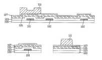
도 1은 종래 기술에 의한 횡전계방식 액정표시소자의 평면도이고, 도 2a 내지 도 2c는 종래 기술에 의한 도 1의 Ⅰ-Ⅰ'선상에서의 공정단면도이다.1 is a plan view of a transverse electric field type liquid crystal display device according to the prior art, and FIGS. 2A to 2C are cross-sectional views of a process along the line II ′ of FIG. 1 according to the prior art.
통상, 횡전계방식 액정표시소자의 박막 어레이 기판 상에는, 도 1에 도시된 바와 같이, 기판 상에 수직으로 교차 배치되어 화소를 정의하는 게이트 배선(12) 및 데이터 배선(15)과, 상기 게이트 배선(12) 및 데이터 배선(15)의 교차 부위에 배치된 박막트랜지스터(TFT)와, 상기 게이트 배선(12)과 평행하도록 화소 내에 배치된 공통배선(25)과, 상기 공통배선(25)에서 분기되어 각 화소영역에 상기 데이터 배선(15)에 평행하도록 형성되는 다수개의 공통전극(24)과, 상기 박막트랜지스터(TFT)의 드레인 전극에 연결되어 각 화소영역의 상기 공통전극(24) 사이에서 상기 공통전극과 평행하게 교차 배치된 다수개의 화소 전극(17)이 구비되어 있다.In general, on the thin film array substrate of the transverse electric field type liquid crystal display device, as shown in FIG. 1, the
상기 박막트랜지스터(TFT)는 상기 게이트 배선(12)에서 분기되는 게이트 전극(12a)과, 상기 게이트 전극(12a)을 포함한 전면에 형성된 게이트 절연막(도시하지 않음)과, 상기 게이트 전극(12a) 상부의 게이트 절연막 상에 형성된 반도체층(14)과, 상기 데이터 배선(15)에서 분기되어 상기 반도체층(14) 양 끝에 각각 형성되는 소스 전극(15a) 및 드레인 전극(15b)으로 구성된다.The thin film transistor TFT may include a
이 때, 도시하지는 않았으나, 상기 게이트 배선(12) 및 데이터 배선(15) 사이에는 실리콘 질화물(SiNx), 실리콘 산화물(SiOx) 등의 무기 재료인 게이트 절연막이 더 구비되고, 상기 데이터 배선(15)과 화소전극(17) 사이에는 실리콘 질화물(SiNx), 실리콘 산화물(SiOx) 등의 무기재료의 단일막이나 또는 상기의 무기재료와 BCB(Benzocyclobutene), 아크릴계 물질과 같은 유기재료를 적층한 이중막의 보호막이 더 구비된다.At this time, although not shown, a gate insulating film made of an inorganic material such as silicon nitride (SiNx) or silicon oxide (SiOx) is further provided between the
그리고, 상기 화소전극(17)은 상기 공통전극(24)과 교번하도록 형성하는데, 공통전극(24)을 먼저 형성하고 화소전극(17)을 이후에 형성하여 그 사이를 절연막 으로써 분리하는 이외에, 상기 화소전극(17)을 먼저 형성하고 공통전극(24)을 이후에 형성하고 그 사이를 절연막으로써 분리하여도 되고, 절연막을 형성하지 않고 상기 공통전극(24) 및 화소전극(17)을 동일층에 형성하여도 된다.The
이하에서는, 상기 공통전극(24) 및 화소전극(17)을 인듐-틴-옥사이드(indium-tin-oxide : ITO)와 같이 빛의 투과율이 비교적 뛰어난 투명도전성 물질로 동일층에 형성하는 ITO-ITO전극 횡전계방식 액정표시소자의 제조방법에 대해 주로 서술한다.Hereinafter, the ITO-ITO in which the
먼저, 도 2a에 도시된 바와 같이, 절연기판(11) 상에 저저항 금속층을 증착한 후, 제 1 마스크를 사용한 포토 및 식각 공정을 통해 선택적으로 패터닝하여 복수개의 게이트 배선(도 1의 12) 및 상기 게이트 배선에서 분기된 형태의 게이트 전극(12a)을 형성한다.First, as shown in FIG. 2A, a low resistance metal layer is deposited on the
다음, 상기 게이트 전극(12a)을 포함한 전면에 실리콘 산화물(SiOx) 또는 실리콘 질화물(SiNx) 등의 무기 절연물질을 증착하여 게이트 절연막(13)을 형성하고, 비정질 실리콘(a-Si:H)을 고온에서 증착한 후, 제 2 마스크를 사용한 포토 및 식각 공정을 통해 선택적으로 패터닝하여 상기 게이트 전극(12a) 상부의 게이트 절연막(13) 상에 반도체층(14)을 형성한다.Next, an inorganic insulating material such as silicon oxide (SiOx) or silicon nitride (SiNx) is deposited on the entire surface including the
계속하여, 도 2b에 도시된 바와 같이, 상기 반도체층(14)을 포함한 전면에 저저항 금속을 증착한 후, 제 3 마스크를 이용한 포토 및 식각 공정을 통해 선택적으로 패터닝하여 복수개의 데이터 배선(15) 및 상기 데이터 배선(15)에서 분기되는 소스/드레인 전극(15a/15b)을 형성한다. 이 때, 상기 저저항 금속으로 비저항이 낮 은 구리(Cu)를 주로 사용하여 RC-딜레이에 의한 화질 저하를 방지한다.Subsequently, as illustrated in FIG. 2B, a low resistance metal is deposited on the entire surface including the
여기서, 상기 데이터 배선(15)은 단위 화소를 정의하기 위해 상기 게이트 배선(12)에 수직하도록 형성하고, 상기 소스/드레인 전극(15a/15b)은 상기 반도체층(14)의 양 끝단에 각각 형성한다.The
다음, 도 2c에 도시된 바와 같이, 상기 데이터 배선(15)을 포함한 전면에 포토 아크릴과 같은 절연막을 증착하여 보호막(26)을 형성한다.Next, as shown in FIG. 2C, an insulating film such as photoacryl is deposited on the entire surface including the
계속하여, 제 4 마스크를 이용한 포토 및 식각 공정을 통해 상기 보호막(26)을 선택적으로 제거하여 상기 드레인 전극(15b)이 노출되는 콘택홀(18)을 형성한다.Subsequently, the
이후, 상기 보호막(26)을 포함한 전면에 ITO(Indium Tin Oxide) 또는 IZO(Indium Zinc Oxide)와 같은 투명도전물질을 증착하고, 제 5 마스크를 이용한 포토 및 식각 공정을 통해 상기 투명도전물질을 선택적으로 패터닝하여 공통배선(도 1의 25), 공통전극(24) 및 화소전극(17)을 형성한다.Thereafter, a transparent conductive material such as indium tin oxide (ITO) or indium zinc oxide (IZO) is deposited on the entire surface including the
여기서, 상기 공통배선(25)은 상기 게이트 배선(12)에 평행하도록 형성하고, 상기 공통전극(24)은 상기 공통 배선(25)에서 분기되어 상기 데이터 배선(15)에 평행하는 형태로 패터닝하며, 상기 화소전극(17)은 상기 콘택홀(18)을 통해 드레인 전극(15b)에 전기적으로 연결되고 상기 공통전극(24)에 평행하도록 형성한다.The
한편, 상기 공통전극(24)을 화소전극(17)을 형성할 때 함께 형성하고 있지만, 게이트 배선을 형성할 때 게이트 전극(12a)과 동일층상에 형성할 수도 있다.The
그러나 상기와 같은 종래의 횡전계방식 액정표시소자 및 그의 제조방법은 총 5마스크(게이트 배선, 반도체층, 데이터 배선, 콘택홀, 화소전극 및 공통전극)를 사용함으로써 공정 단가가 증가하고 공정이 복잡하다는 문제를 가지고 있었다.However, the conventional transverse electric field type liquid crystal display device and its manufacturing method use a total of five masks (gate wiring, semiconductor layer, data wiring, contact hole, pixel electrode, and common electrode), which increases the process cost and the complexity of the process. Had a problem.
본 발명은 상기와 같은 문제점을 해결하기 위해 안출한 것으로서, 리프트-오프 공정을 이용하여 마스크의 사용횟수를 줄임으로써 공정 단가를 절감하고 공정시간을 단축하는 횡전계방식 액정표시소자의 제조방법을 제공하는데 그 목적이 있다.The present invention has been made to solve the above problems, and provides a method of manufacturing a transverse electric field type liquid crystal display device which reduces the process cost and shorten the process time by reducing the number of times of use of the mask using a lift-off process. Its purpose is to.
삭제delete
상기와 같은 목적을 달성하기 위한 본 발명에 의한 횡전계방식 액정표시소자의 제조방법은 기판상에 금속을 증착한 후 제 1 마스크를 이용한 포토 및 식각 공정을 통해 상기 금속을 선택적으로 패터닝하여 게이트 라인, 상기 게이트 라인과 접속된 게이트 전극, 상기 게이트 라인과 일정한 간격을 갖고 화소영역을 둘러싸는 공통라인을 형성하는 단계; 상기 게이트 라인을 포함한 전면에 게이트 절연막을 형성하는 단계; 상기 게이트 절연막상에 비정질 실리콘층 및 금속층을 차례로 형성하고 상기 금속층상에 제 1 포토레지스트를 도포하는 단계; 상기 제 1 포토레지스트의 상부에 투과영역, 차단영역 및 슬릿영역을 갖는 제 2 마스크를 정렬하고 회절 노광 및 현상 공정을 통해 패터닝하는 단계; 상기 패터닝된 제 1 포토레지스트를 마스크로 하여 상기 금속층 및 비정질 실리콘층을 선택적으로 식각하여 액티브층 및 금속막 패턴을 형성하는 단계; 상기 패터닝된 제 1 포토레지스트를 애싱 처리하고, 상기 애싱 처리된 제 1 포토레지스트를 마스크로 이용하여 상기 금속막 패턴을 선택적으로 제거하여 상기 게이트 라인과 수직하고 상기 공통라인과 일정한 간격을 갖는 데이터 라인, 상기 데이터 라인과 접속된 소오스 전극, 상기 소오스 전극과 일정한 간격을 갖는 드레인 전극을 형성하는 단계; 상기 데이터 라인을 포함한 기판의 전면에 보호막을 형성하는 단계; 상기 보호막상에 제 2 포토레지스트를 도포하고, 제 3 마스크를 사용하여 노광 및 현상 공정을 통해 상기 제 2 포토레지스트를 선택적으로 패터닝하는 단계; 상기 패터닝된 제 2 포토레지스트를 마스크로 하여 상기 공통라인 및 드레인 전극의 표면이 소정부분 노출되도록 상기 보호막을 선택적으로 제거하여 복수개의 콘택홀을 형성하는 단계; 상기 각 콘택홀을 포함한 제 2 포토레지스트의 전면에 투명 도전물질을 형성하는 단계; 상기 제 2 포토레지스트와 함께 상부의 투명 도전물질을 제거하여 상기 각 콘택홀을 통해 상기 드레인 전극과 연결되는 화소전극 및 상기 공통라인에 연결되는 공통전극을 형성하는 단계를 포함하여 이루어짐을 특징으로 한다.In the method of manufacturing a transverse electric field type liquid crystal display device according to the present invention for achieving the above object, a gate line by selectively patterning the metal through a photo and etching process using a first mask after depositing a metal on a substrate Forming a gate line connected to the gate line and a common line surrounding the pixel area at a predetermined distance from the gate line; Forming a gate insulating film on the entire surface including the gate line; Sequentially forming an amorphous silicon layer and a metal layer on the gate insulating film and applying a first photoresist on the metal layer; Arranging a second mask having a transmission region, a blocking region, and a slit region on top of the first photoresist and patterning the photomask through a diffraction exposure and development process; Selectively etching the metal layer and the amorphous silicon layer using the patterned first photoresist as a mask to form an active layer and a metal film pattern; Ashing the patterned first photoresist, and selectively removing the metal layer pattern using the ashed first photoresist as a mask so as to be perpendicular to the gate line and have a constant distance from the common line Forming a source electrode connected to the data line and a drain electrode having a predetermined distance from the source electrode; Forming a protective film on an entire surface of the substrate including the data line; Applying a second photoresist on the passivation layer and selectively patterning the second photoresist through an exposure and development process using a third mask; Forming a plurality of contact holes by selectively removing the passivation layer so that the surfaces of the common line and the drain electrode are partially exposed using the patterned second photoresist as a mask; Forming a transparent conductive material on the entire surface of the second photoresist including each of the contact holes; And removing the transparent conductive material on the upper portion together with the second photoresist to form a pixel electrode connected to the drain electrode and a common electrode connected to the common line through each contact hole. .
이하, 첨부된 도면을 참고하여 본 발명에 따른 횡전계방식 액정표시소자의 제조방법을 상세히 설명하면 다음과 같다.Hereinafter, a method of manufacturing a transverse electric field type liquid crystal display device according to the present invention will be described in detail with reference to the accompanying drawings.
도 3은 본 발명에 따른 횡전계방식 액정표시소자를 나타낸 평면도이고, 도 4는 도 3의 Ⅳ-Ⅳ'선에 따른 횡전계방식 액정표시소자를 나타낸 단면도이다.3 is a plan view showing a transverse electric field liquid crystal display device according to the present invention, Figure 4 is a cross-sectional view showing a transverse electric field liquid crystal display device along the line IV-IV 'of FIG.
도 3 및 도 4에 도시한 바와 같이, 기판(100)상에 일방향으로 형성되는 게이트 라인(121)과, 상기 게이트 라인(121)으로부터 돌출되어 형성되는 게이트 전극(101)과, 상기 게이트 라인(101)과 일정한 간격을 갖고 동일한 방향을 갖고 사각형 형태로 형성되는 공통라인(102)과, 상기 게이트 전극(101) 및 게이트 라인(121)을 포함한 기판(100)의 전면에 형성되는 게이트 절연막(103)과, 상기 게이트 전극(101)과 대응되는 게이트 절연막(103)상에 형성되는 반도체층(105a)과, 상기 반도체층(105a)상에 상기 게이트 라인(121)과 교차하면서 화소영역을 정의하 고 상기 공통라인(102)과 일정한 간격을 갖고 형성되는 데이터 라인(122) 및 상기 데이터 라인(122)으로부터 연장되는 소오스 전극(107a)과 상기 소오스 전극(107a)과 일정한 간격을 갖고 형성되는 드레인 전극(107b)과, 상기 드레인 전극(107b) 및 공통라인의 표면이 소정부분 노출되도록 콘택홀을 갖고 기판(100)의 전면에 형성되는 보호막(106)과, 상기 콘택홀을 통해 상기 드레인 전극(107b)과 연결되어 형성되는 화소전극(115a) 및 상기 화소전극(115a)과 일정한 간격을 갖고 상기 공통라인(102)에 접속되는 공통전극(115b)을 포함하여 구성되어 있다.3 and 4, the
여기서, 상기 소오스 전극(107a)은 U자형 구조를 갖고 있고, 상기 소오스 전극(107a)과 일정한 간격을 갖고 게이트 절연막(103)상에 상기 게이트 라인(101a)과 오버랩되게 캐패시터 전극이 형성되어 있다.Here, the
또한, 상기 공통라인(102)과 드레인 전극(107b)은 소정부분이 오버랩되어 있고, 상기 드레인 전극(107b)에 연결되는 화소전극(115a)은 일정한 간격을 갖고 형성되며 상기 각 화소전극(115a) 사이에는 상기 공통라인(102)과 연결되는 공통전극(115b)이 형성된다.In addition, a predetermined portion of the
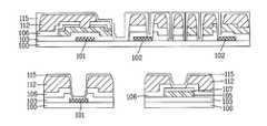
도 5a 내지 5h는 본 발명에 따른 횡전계방식 액정표시소자의 제조방법을 나타낸 공정단면도이다.5A to 5H are cross-sectional views illustrating a method of manufacturing a transverse electric field type liquid crystal display device according to the present invention.
도 5a에 도시된 바와 같이, 기판(100) 상에 낮은 비저항을 가지는 구리(Cu), 알루미늄(Al), 알루미늄 합금(AlNd : Aluminum Neodymium), 몰리브덴(Mo), 크롬(Cr), 티타늄(Ti), 탄탈륨(Ta), 몰리브덴-텅스텐(MoW) 등의 금속을 증착한 후, 제 1 마스크를 이용한 포토 및 식각공정을 통해 상기 금속을 선택적으로 패터닝하 여 게이트 라인(도 3의 121) 및 상기 게이트 라인(121)에서 돌출되는 게이트 전극(101) 그리고 상기 게이트 라인(121)과 일정한 간격을 갖는 사각형 형상의 공통라인(102)을 형성한다.As shown in FIG. 5A, copper (Cu), aluminum (Al), aluminum alloy (AlNd: Aluminum Neodymium), molybdenum (Mo), chromium (Cr), and titanium (Ti) having a low resistivity on the substrate 100 ), Tantalum (Ta), molybdenum-tungsten (MoW), and the like, and then selectively patterning the metal through a photo-etching process using a first mask to form a gate line (121 of FIG. 3) and the
다음, 도 5b에 도시한 바와 같이, 상기 게이트 전극(101)을 포함한 전면에 실리콘 산화물(SiOx) 또는 실리콘 질화물(SiNx)등의 무기 절연물질을 통상, 플라즈마 강화형 화학 증기 증착(PECVD : plasma enhanced chemical vapor deposition) 방법으로 증착하여 게이트 절연막(103)을 형성한다.Next, as shown in FIG. 5B, an inorganic insulating material such as silicon oxide (SiOx) or silicon nitride (SiNx) is generally disposed on the entire surface including the
이어서, 상기 게이트 절연막(103)을 포함한 전면에 비정질 실리콘(a-Si:H)층(105)을 고온에서 증착한다.Subsequently, an amorphous silicon (a-Si: H)
여기서, 상기 비정질 실리콘층(105) 상에는 이후 형성될 소스/드레인 전극과의 콘택 저항을 낮추기 위해 비정질 실리콘에 불순물을 도핑한 오버코트층을 더 형성할 수 있다.Here, an overcoat layer doped with impurities may be further formed on the
계속하여, 상기 비정질 실리콘층(105)상에 구리(Cu), 알루미늄(Al), 알루미늄 합금(AlNd : Aluminum Neodymium), 몰리브덴(Mo), 크롬(Cr), 티타늄(Ti), 탄탈륨(Ta), 몰리브덴-텅스텐(MoW) 등의 금속층(107)을 증착한다.Subsequently, on the
다음으로, 상기 금속층(107)의 전면에 포토레지스트(111)를 도포하고, 상기 포토레지스트(111)의 상부에 회절마스크(미 도시)를 정렬한다.Next, a
여기서, 상기 회절마스크는 광을 투과시키는 투과영역과, 광을 차단시키는 차단영역과, 광의 일부분은 투과시키고 일부분은 차단시키는 슬릿영역으로 이루어져 있다.The diffraction mask includes a transmission region for transmitting light, a blocking region for blocking light, and a slit region for transmitting a portion of light and blocking a portion of the light.
이와 같이 구성된 회절마스크를 통해 상기 포토레지스트(111)에 자외선과 같은 광을 조사시키는 노광 및 현상공정을 진행하면, 상기 투과영역에 대응하는 포토레지스트는 모두 제거되고, 상기 차단영역에 대응하는 포토레지스트(111)는 그대로 남아있게 되며, 상기 슬릿영역에 대응하는 포토레지스트(111)는 일정 두께만 제거된다.When the exposure and development processes of irradiating the
통상적으로 상기 슬릿영역에 대응하는 포토레지스트(111)는 약 반정도의 두께가 남게 되는데, 이와 같이 남게 되는 포토레지스트(111)를 하프톤(half tone) 레지스트라고 한다.Typically, the
이후, 도 5c에 도시한 바와 같이, 상기 패터닝된 포토레지스트(111)를 마스크로 하여 노출되는 금속층(107) 및 비정질 실리콘층(105)을 선택적으로 식각하여 액티브층(105a) 및 금속막 패턴을 형성한다.Subsequently, as shown in FIG. 5C, the exposed
도 5d에 도시한 바와 같이, 상기 패터닝된 포토레지스트(111)를 산소(O2) 플라즈마처리 하여 애싱한다.As shown in FIG. 5D, the patterned
여기서, 상기 애싱공정에 의해 상기 패터닝된 포토레지스트(111) 및 상기 하프톤 레지스트는 동일한 수준으로 제거되며, 이때, 상기 하프톤 레지스트는 상기 패터닝된 포토레지스트(111)의 두께보다 얇기 때문에 상기 하프톤 레지스트가 제거된 영역에는 금속층(107)이 노출된다.Here, the patterned
이어서, 상기 애싱처리된 포토레지스트(111)를 마스크로 이용하여 상기 금속층(107)을 선택적으로 제거하여 상기 게이트 라인(121)과 수직한 방향의 데이터 라 인(도 3의 122) 및 상기 데이터 라인(122)에서 돌출되는 소오스 전극(107a)과 상기 소오스 전극(107a)과 일정한 간격을 갖는 드레인 전극(107b)을 상기 액티브층(105a)상에 형성한다.Subsequently, the
다음, 도 5e에 도시된 바와 같이, 상기 소오스 전극(107a) 및 드레인 전극(107b)을 포함한 기판(100)의 전면에 유기 절연막 등을 사용하여 보호막(106)을 형성한다.Next, as shown in FIG. 5E, the
그리고, 상기 보호막(106) 상에 포토레지스트(112)를 도포한 후, 노광 및 현상 공정을 통해 상기 포토레지스트(112)를 선택적으로 패터닝한다.After the
이어서, 도 5f에 도시한 바와 같이, 상기 패터닝된 포토레지스트(112)를 마스크로 하여 상기 드레인 전극(107a) 및 공통라인(102)의 표면이 소정부분 노출되도록 상기 보호막(106)을 선택적으로 식각하여 콘택홀을 형성한다.Subsequently, as shown in FIG. 5F, the
여기서, 상기 보호막(106)을 식각하는 것은 후의 리프트-오프(Lift-Off) 공정시 스트리퍼 용액이 침투할 수 있도록 경로를 만들어 주기 위해서이다.In this case, the
다음으로, 도 5g에 도시된 바와 같이, 상기 패터닝된 포토레지스트(112)를 포함한 기판(100)의 전면에 투명 도전물질(115)을 증착한다.Next, as illustrated in FIG. 5G, the transparent
상기 투명 도전물질(115)은 ITO(Indium Tin Oxide) 또는 IZO(Indium Zinc Oxide)와 같은 물질로 한다.The transparent
이후, 도 5h에 도시한 바와 같이, 스트리퍼 용액을 사용하여 상기 패터닝된 포토레지스트(112)를 제거하면, 상기 패터닝된 포토레지스트(112)의 상부에 형성된 투명 도전물질(115)도 같이 떨어져 나가며, 상기 떨어져 나간 투명 도전물질(115) 의 파티클은 상기 스트리퍼 용액에 의해 용해되어 제거된다.Thereafter, as shown in FIG. 5H, when the patterned
즉, 상기 포토레지스트(112) 상부의 투명 도전물질(115)이 제거되면서 상기 드레인 전극(107a)과 연결되는 화소전극(115a) 및 상기 화소전극(115a)과 일정한 간격을 갖고 상기 공통라인(102)에 연결되는 공통전극(115b)을 형성한다.That is, while the transparent
여기서, 상기 스트리퍼 용액을 사용하여 상기 패터닝된 포토레지스트(112)를 제거함과 동시에 상기 패터닝된 포토레지스트(112)의 상부에 증착된 투명 도전물질(115)을 제거하는 방식을 리프트-오프법이라고 한다.Here, a method of removing the patterned
이와 같이, 상기 리프트-오프 공정을 이용하여 화소 전극(115a) 및 공통전극(115b)을 형성함으로써, 마스크의 사용 횟수를 1회 저감할 수 있다.As described above, the
따라서, 본 발명에서는 3번의 마스크를 사용하여 횡전계방식 액정표시소자를 구현할 수 있다.Therefore, in the present invention, the transverse electric field type liquid crystal display device can be realized by using the third mask.
이와 같이, 리프트-오프 공정을 이용한 기판(100)은 도시하지는 않았으나, 상기 기판(100)에 컬러필터층 및 블랙 매트릭스층이 형성된 다른 기판을 대향 합착한 후, 상기 두 기판 사이에 액정층을 형성하고 액정 주입구를 밀봉함으로써 횡전계방식 액정표시소자를 완성할 수 있다.As such, although the
이상 설명한 내용을 통해 당업자라면 본 발명의 기술사상을 일탈하지 아니하는 범위에서 다양한 변경 및 수정이 가능함을 알 수 있을 것이다. 따라서, 본 발명의 기술적 범위는 명세서의 상세한 설명에 기재된 내용으로 한정되는 것이 아니라 특허 청구의 범위에 의해 정해져야만 할 것이다.Those skilled in the art will appreciate that various changes and modifications can be made without departing from the technical spirit of the present invention. Therefore, the technical scope of the present invention should not be limited to the contents described in the detailed description of the specification but should be defined by the claims.
이상 설명한 바와 같이, 본 발명에 따른 횡전계방식 액정표시소자의 제조방법은 리프트-오프 공정을 이용하여 마스크의 사용횟수를 줄임으로써 공정 단가를 절감하고 공정시간을 단축하여 생산 수율을 향상시키는 효과가 있다.As described above, the method of manufacturing the transverse electric field type liquid crystal display device according to the present invention has an effect of reducing the production cost by reducing the number of times of use of the mask using a lift-off process and shortening the processing time to improve the production yield. have.
Claims (12)
Translated fromKoreanPriority Applications (1)
| Application Number | Priority Date | Filing Date | Title |
|---|---|---|---|
| KR1020030101425AKR101048699B1 (en) | 2003-12-31 | 2003-12-31 | Method of manufacturing a transverse electric field type liquid crystal display device |
Applications Claiming Priority (1)
| Application Number | Priority Date | Filing Date | Title |
|---|---|---|---|
| KR1020030101425AKR101048699B1 (en) | 2003-12-31 | 2003-12-31 | Method of manufacturing a transverse electric field type liquid crystal display device |
Publications (2)
| Publication Number | Publication Date |
|---|---|
| KR20050069383A KR20050069383A (en) | 2005-07-05 |
| KR101048699B1true KR101048699B1 (en) | 2011-07-12 |
Family
ID=37259799
Family Applications (1)
| Application Number | Title | Priority Date | Filing Date |
|---|---|---|---|
| KR1020030101425AExpired - Fee RelatedKR101048699B1 (en) | 2003-12-31 | 2003-12-31 | Method of manufacturing a transverse electric field type liquid crystal display device |
Country Status (1)
| Country | Link |
|---|---|
| KR (1) | KR101048699B1 (en) |
Families Citing this family (3)
| Publication number | Priority date | Publication date | Assignee | Title |
|---|---|---|---|---|
| KR101282898B1 (en)* | 2006-06-30 | 2013-07-05 | 엘지디스플레이 주식회사 | In-Plane Switching Mode Liquid Crystal Display Device and the method for fabricating thereof |
| KR101327851B1 (en)* | 2007-02-07 | 2013-11-12 | 엘지디스플레이 주식회사 | Method for forming copper line and method for manufacturing liquid crystal display using the same |
| KR101358221B1 (en)* | 2007-05-31 | 2014-02-05 | 엘지디스플레이 주식회사 | In plane switching mode liquid crystal display device and method of fabricating the same |
Citations (3)
| Publication number | Priority date | Publication date | Assignee | Title |
|---|---|---|---|---|
| KR100322969B1 (en)* | 1999-12-22 | 2002-02-01 | 주식회사 현대 디스플레이 테크놀로지 | In-plane switching mode lcd and method for fabricating the same |
| KR20020057019A (en)* | 2000-12-30 | 2002-07-11 | 주식회사 현대 디스플레이 테크놀로지 | Method for manufacturing thin film transistor lcd |
| KR20030058511A (en)* | 2001-12-31 | 2003-07-07 | 비오이 하이디스 테크놀로지 주식회사 | A method for manufacturing of thin film transistor liquid crystal display |
- 2003
- 2003-12-31KRKR1020030101425Apatent/KR101048699B1/ennot_activeExpired - Fee Related
Patent Citations (3)
| Publication number | Priority date | Publication date | Assignee | Title |
|---|---|---|---|---|
| KR100322969B1 (en)* | 1999-12-22 | 2002-02-01 | 주식회사 현대 디스플레이 테크놀로지 | In-plane switching mode lcd and method for fabricating the same |
| KR20020057019A (en)* | 2000-12-30 | 2002-07-11 | 주식회사 현대 디스플레이 테크놀로지 | Method for manufacturing thin film transistor lcd |
| KR20030058511A (en)* | 2001-12-31 | 2003-07-07 | 비오이 하이디스 테크놀로지 주식회사 | A method for manufacturing of thin film transistor liquid crystal display |
Also Published As
| Publication number | Publication date |
|---|---|
| KR20050069383A (en) | 2005-07-05 |
Similar Documents
| Publication | Publication Date | Title |
|---|---|---|
| US8933460B2 (en) | Array substrate for fringe field switching mode liquid crystal display device | |
| US7489380B2 (en) | Thin film transistor substrate of horizontal electric field applying type and fabricating method thereof | |
| US6281957B1 (en) | In-plane switching mode liquid crystal display device | |
| KR100682358B1 (en) | LCD panel and manufacturing method | |
| US7118947B2 (en) | Thin film transistor substrate of a horizontal electric field type LCD and fabricating method thereof | |
| US7561236B2 (en) | Method of fabricating array substrate for in-plane switching liquid crystal display device | |
| US8803147B2 (en) | Array substrate for fringe field switching mode liquid crystal display device and method of manufacturing the same | |
| US20080073651A1 (en) | Liquid crystal display device | |
| US20090137077A1 (en) | Thin film transistor array substrate and fabricating method thereof | |
| US20150153600A1 (en) | Liquid crystal display and method for manufacturing the same | |
| US20130295701A1 (en) | Liquid crystal display of horizontal electronic field applying type and fabricating method thereof | |
| US7061566B2 (en) | In-plane switching mode liquid crystal display device and method of fabricating the same | |
| US20100220255A1 (en) | Array substrate for fringe field switching mode liquid crystal display device | |
| US7289180B2 (en) | Liquid crystal display device of a horizontal electric field applying type comprising a storage capacitor substantially parallel to the data line and fabricating method thereof | |
| KR101423909B1 (en) | Display substrate and liquid crystal display device having the same | |
| KR101321242B1 (en) | In-Plane-Switching mode Liquid Crystal Display device and the fabrication method thereof | |
| KR101048699B1 (en) | Method of manufacturing a transverse electric field type liquid crystal display device | |
| KR101399154B1 (en) | Liquid crystal display device and method of manufacturing the same | |
| KR101055201B1 (en) | Manufacturing method of COT type liquid crystal display device | |
| KR101255274B1 (en) | The in-plane switching mode liquid crystal display device and method for fabricating the same | |
| KR20080045362A (en) | Liquid Crystal Display and Manufacturing Method Thereof | |
| KR101149938B1 (en) | Fabricating method of thin film transistor substrate of fringe field switch type | |
| KR101308443B1 (en) | In-plane switching mode liquid crystal display device and method for fabricating the same | |
| KR20080049443A (en) | Transverse electric field liquid crystal display device and manufacturing method thereof | |
| KR101116819B1 (en) | Method For Fabricating Liquid Crystal Display Panel |
Legal Events
| Date | Code | Title | Description |
|---|---|---|---|
| PA0109 | Patent application | St.27 status event code:A-0-1-A10-A12-nap-PA0109 | |
| PG1501 | Laying open of application | St.27 status event code:A-1-1-Q10-Q12-nap-PG1501 | |
| PN2301 | Change of applicant | St.27 status event code:A-3-3-R10-R13-asn-PN2301 St.27 status event code:A-3-3-R10-R11-asn-PN2301 | |
| A201 | Request for examination | ||
| PA0201 | Request for examination | St.27 status event code:A-1-2-D10-D11-exm-PA0201 | |
| E902 | Notification of reason for refusal | ||
| PE0902 | Notice of grounds for rejection | St.27 status event code:A-1-2-D10-D21-exm-PE0902 | |
| E13-X000 | Pre-grant limitation requested | St.27 status event code:A-2-3-E10-E13-lim-X000 | |
| P11-X000 | Amendment of application requested | St.27 status event code:A-2-2-P10-P11-nap-X000 | |
| P13-X000 | Application amended | St.27 status event code:A-2-2-P10-P13-nap-X000 | |
| R18-X000 | Changes to party contact information recorded | St.27 status event code:A-3-3-R10-R18-oth-X000 | |
| E902 | Notification of reason for refusal | ||
| PE0902 | Notice of grounds for rejection | St.27 status event code:A-1-2-D10-D21-exm-PE0902 | |
| P11-X000 | Amendment of application requested | St.27 status event code:A-2-2-P10-P11-nap-X000 | |
| P13-X000 | Application amended | St.27 status event code:A-2-2-P10-P13-nap-X000 | |
| E701 | Decision to grant or registration of patent right | ||
| PE0701 | Decision of registration | St.27 status event code:A-1-2-D10-D22-exm-PE0701 | |
| GRNT | Written decision to grant | ||
| PR0701 | Registration of establishment | St.27 status event code:A-2-4-F10-F11-exm-PR0701 | |
| PR1002 | Payment of registration fee | St.27 status event code:A-2-2-U10-U11-oth-PR1002 Fee payment year number:1 | |
| PG1601 | Publication of registration | St.27 status event code:A-4-4-Q10-Q13-nap-PG1601 | |
| R18-X000 | Changes to party contact information recorded | St.27 status event code:A-5-5-R10-R18-oth-X000 | |
| R18-X000 | Changes to party contact information recorded | St.27 status event code:A-5-5-R10-R18-oth-X000 | |
| FPAY | Annual fee payment | Payment date:20140630 Year of fee payment:4 | |
| PR1001 | Payment of annual fee | St.27 status event code:A-4-4-U10-U11-oth-PR1001 Fee payment year number:4 | |
| FPAY | Annual fee payment | Payment date:20150629 Year of fee payment:5 | |
| PR1001 | Payment of annual fee | St.27 status event code:A-4-4-U10-U11-oth-PR1001 Fee payment year number:5 | |
| FPAY | Annual fee payment | Payment date:20160630 Year of fee payment:6 | |
| PR1001 | Payment of annual fee | St.27 status event code:A-4-4-U10-U11-oth-PR1001 Fee payment year number:6 | |
| P22-X000 | Classification modified | St.27 status event code:A-4-4-P10-P22-nap-X000 | |
| PR1001 | Payment of annual fee | St.27 status event code:A-4-4-U10-U11-oth-PR1001 Fee payment year number:7 | |
| LAPS | Lapse due to unpaid annual fee | ||
| PC1903 | Unpaid annual fee | St.27 status event code:A-4-4-U10-U13-oth-PC1903 Not in force date:20180707 Payment event data comment text:Termination Category : DEFAULT_OF_REGISTRATION_FEE | |
| PC1903 | Unpaid annual fee | St.27 status event code:N-4-6-H10-H13-oth-PC1903 Ip right cessation event data comment text:Termination Category : DEFAULT_OF_REGISTRATION_FEE Not in force date:20180707 |