KR101047691B1 - Semiconductor light emitting device and manufacturing method thereof - Google Patents
Semiconductor light emitting device and manufacturing method thereofDownload PDFInfo
- Publication number
- KR101047691B1 KR101047691B1KR1020080126827AKR20080126827AKR101047691B1KR 101047691 B1KR101047691 B1KR 101047691B1KR 1020080126827 AKR1020080126827 AKR 1020080126827AKR 20080126827 AKR20080126827 AKR 20080126827AKR 101047691 B1KR101047691 B1KR 101047691B1
- Authority
- KR
- South Korea
- Prior art keywords
- layer
- semiconductor layer
- undoped
- conductive
- conductive semiconductor
- Prior art date
- Legal status (The legal status is an assumption and is not a legal conclusion. Google has not performed a legal analysis and makes no representation as to the accuracy of the status listed.)
- Active
Links
Images


Landscapes
- Led Devices (AREA)
Abstract
Translated fromKoreanDescription
Translated fromKorean실시 예는 반도체 발광소자 및 그 제조방법이 개시된다.The embodiment discloses a semiconductor light emitting device and a method of manufacturing the same.
일반적으로 반도체 발광소자는 자외선, 청색 및 녹색 영역을 포괄하는 발광 영역을 가진다. 특히, GaN계 질화물 반도체 발광소자는 그 응용 분야에 있어서 청색 LED, 녹색 LED 등의 광소자 및 MESFET(Metal Semiconductor Field Effect Transistor), HEMT (Hetero junction Field - Effect Transistors) 등의 고속 스위칭 소자, 고출력 소자, 표시장치 및 지시기 등에 응용되고 있다.In general, a semiconductor light emitting device has a light emitting area covering an ultraviolet, blue and green area. Particularly, GaN-based nitride semiconductor light emitting devices include optical devices such as blue LEDs and green LEDs, high-speed switching devices such as metal semiconductor field effect transistors (MESFETs), and hetero junction field-effect transistors (HEMTs), and high output devices. It is applied to display devices and indicators.
실시 예는 활성층 위의 반도체층에서의 전류 분포가 개선될 수 있도록 한 반도체 발광소자 및 그 제조방법을 제공한다.The embodiment provides a semiconductor light emitting device and a method of manufacturing the same so that current distribution in a semiconductor layer on an active layer can be improved.
실시 예는 제2도전형 반도체층 위 또는/및 아래에 적어도 한 층의 언도프드 반도체층을 형성해 주어, 상기 제2도전형 반도체층을 통해 활성층으로 공급되는 캐리어의 수평 방향으로의 흐름을 개선시켜 줄 수 있도록 한 반도체 발광소자 및 그 제조방법을 제공한다.The embodiment forms at least one undoped semiconductor layer above or below the second conductive semiconductor layer, thereby improving the flow in the horizontal direction of the carrier supplied to the active layer through the second conductive semiconductor layer. A semiconductor light emitting device and a method of manufacturing the same are provided.
실시 예는 제2도전형 반도체층 위에 언도프드 반도체층 및 상기 제2도전형 반도체층 보다 도펀트 농도가 높은 고농도의 도전형 반도체층을 형성시켜 주어, 상기 도전형 반도체층을 통해 활성층으로 공급되는 캐리어의 수평 방향으로의 흐름을 개선시켜 줄 수 있도록 한 반도체 발광소자 및 그 제조방법을 제공한다.The embodiment forms a high concentration conductive semiconductor layer having a higher dopant concentration than the second conductive semiconductor layer and an undoped semiconductor layer on the second conductive semiconductor layer, and is supplied to the active layer through the conductive semiconductor layer. A semiconductor light emitting device and a method of manufacturing the same are provided to improve flow in a horizontal direction.
실시 예에 따른 반도체 발광소자는, 제 1도전형 반도체층; 상기 제 1도전형 반도체층 위에 형성된 활성층; 상기 활성층 위에 형성된 제2도전형 반도체층, 상기 제2도전형 반도체층 위에 형성된 언도프드 반도체층; 상기 언도프드 반도체층 위에 형성된 고농도의 제2도전형 반도체층을 포함하는 제2도전형 구조물을 포함한다.A semiconductor light emitting device according to an embodiment includes a first conductive semiconductor layer; An active layer formed on the first conductive semiconductor layer; A second conductive semiconductor layer formed on the active layer, an undoped semiconductor layer formed on the second conductive semiconductor layer; And a second conductive structure including a high concentration of the second conductive semiconductor layer formed on the undoped semiconductor layer.
실시 예에 따른 반도체 발광소자 제조방법은, 제 1도전형 반도체층 위에 활성층을 형성하는 단계; 상기 활성층 위에 제 2도전형 구조물을 형성하는 단계를 포함하며, 상기 제2도전형 구조물은 상기 활성층 위에 제2도전형 반도체층을 형성하 는 단계; 상기 제2도전형 반도체층 위에 언도프드 반도체층을 형성하는 단계; 상기 언도프드 반도체층 위에 고농도의 제2도전형 반도체층을 형성하는 단계를 포함한다.A method of manufacturing a semiconductor light emitting device according to an embodiment includes: forming an active layer on a first conductive semiconductor layer; Forming a second conductive structure over the active layer, wherein the second conductive structure comprises forming a second conductive semiconductor layer over the active layer; Forming an undoped semiconductor layer on the second conductive semiconductor layer; Forming a high concentration of the second conductive semiconductor layer on the undoped semiconductor layer.
실시 예는 전류 확산 구조를 갖는 제2도전형 구조물에 의해 활성층으로 공급되는 전류 흐름을 개선시켜 줄 수 있다.The embodiment can improve the flow of current supplied to the active layer by the second conductive structure having the current spreading structure.
실시 예는 활성층 위에서의 전류 분포를 분산시켜 줌으로써, ESD에 강한 발광 소자를 제공할 수 있다.The embodiment can provide a light emitting device resistant to ESD by dispersing a current distribution on the active layer.
이하, 첨부된 도면을 참조하여 실시 예를 설명하면 다음과 같다. 이하, 실시 예를 설명함에 있어서, 각 층은 두께는 일 예이며, 도면에 도시된 두께로 한정하지 않는다.Hereinafter, exemplary embodiments will be described with reference to the accompanying drawings. Hereinafter, in describing the embodiments, the thickness of each layer is one example, and is not limited to the thickness shown in the drawings.
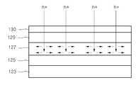
도 1은 제 1실시 예에 따른 반도체 발광소자의 측 단면도이며, 도 2는 도 1의 고농도의 제2도전형 반도체층에서의 전류 확산 방향을 일 예를 나타낸 도면이다.1 is a side cross-sectional view of a semiconductor light emitting device according to a first embodiment, and FIG. 2 is a diagram illustrating an example of a current diffusion direction in the second conductive semiconductor layer of high concentration shown in FIG. 1.
도 1을 참조하면, 반도체 발광소자(100)는 기판(110), 버퍼층(112), 하부 언도프드 반도체층(114), 제 1도전형 반도체층(116), 활성층(118), 제 2도전형 구조물(120), 제 3도전형 반도체층(130)을 포함한다.Referring to FIG. 1, the semiconductor
상기 기판(110)은 사파이어 기판(Al203), SiC, Si, GaAs, GaN, ZnO, GaP, InP, Ge 중 적어도 하나를 이용할 수 있으며, 도전 특성을 갖는 기판으로 이용할 수도 있다. 상기 기판(110)은 최종 소자에서 제거될 수도 있다. 상기 기판(110)의 위 또는/및 아래에는 요철 패턴이 형성될 수 있으며, 상기 요철 패턴은 형상은 스트라이프 형태, 렌즈 형태, 기둥 형태, 뿔 형태 중 어느 하나를 포함할 수 있다.The
상기 기판(110) 위에는 질화물 반도체가 성장되는 데, 성장 장비는 전자빔 증착기, PVD(physical vapor deposition), CVD(chemical vapor deposition), PLD(plasma laser deposition), 이중형의 열증착기(dual-type thermal evaporator) 스퍼터링(sputtering), MOCVD(metal organic chemical vapor deposition) 등에 의해 형성할 수 있으며, 이러한 장비로 한정하지는 않는다. 상기 반도체는 InxAlyGa1-x-yN (0≤x≤1, 0≤y≤1, 0≤x+y≤1)의 조성식을 갖는 화합물 반도체로 구현된다.The nitride semiconductor is grown on the
상기 기판(110) 위에는 버퍼층(112)이 형성된다. 상기 버퍼층(112)은 GaN 재료와 기판 재료의 격자 부정합을 완화시켜 줄 수 있으며, GaN, InN, AlN, InGaN, AlGaN, InAlGaN, AlInN 중 적어도 하나로 형성될 수 있다. 상기 버퍼층(112)은 도전형 도펀트가 도핑될 수도 있고, 도핑되지 않을 수도 있다.The
상기 버퍼층(112) 위에는 하부 언도프드 반도체층(114)이 형성된다. 상기 하부 언도프드 반도체층(114)은 제1도전형 도펀트 또는 제2도전형 도펀트를 첨가하지 않는 undoped GaN계층으로 형성될 수 있다. 상기 버퍼층(112) 및/또는 하부 언도프드 반도체층(114)은 형성하지 않거나, 최종 소자에 존재하지 않을 수도 있다.The lower
상기 제1도전형 반도체층(116)은 제1도전형 도펀트가 도핑된 적어도 한 반도체층으로 이루어질 수 있으며, 제1전극 접촉층으로 기능할 수 있다. 상기 제1도전 형 반도체층(116)은 GaN, InN, AlN, InGaN, AlGaN, InAlGaN, AlInN 중 적어도 하나로 형성될 수 있으며, 상기 제1도전형 도펀트는 예컨대, n형 도펀트로서 Si, Ge, Sn , Se, Te를 포함한다.The first
상기 제1도전형 반도체층(116) 위에는 활성층(118)이 형성된다. 상기 활성층(118)은 단일 양자 우물 또는 다중 양자 우물(MQW) 구조로 형성되며, InGaN/GaN 또는 AlGaN/GaN로 형성될 수 있다. 상기 활성층(118)은 발광시키는 빛의 파장에 따른 밴드 갭 에너지를 갖는 재료로 선택되며, 예를 들면, 파장이 460~470nm의 청색 발광의 경우, InxGa1-xN 우물층/InyGa1-yN 장벽층을 한 주기로 하여, 단일 또는 다중 양자 우물 구조로 형성될 수 있다. 여기서, 상기 우물층 InxGa1-xN은 0≤x≤1, 장벽층 InyGa1-yN은 0≤x≤1으로 조절할 수 있다. 상기 활성층(118)은 청색 파장의 광, 레드 파장의 광, 녹색 파장의 광 등의 유색 광을 발광하는 재료를 포함할 수 있다.An
상기 제1도전형 반도체층(116)과 활성층(118) 사이에는 제1도전형 AlGaN층이 형성될 수 있으며, 상기 제1도전형 AlGaN층은 클래드층으로 기능할 수 있다.A first conductive AlGaN layer may be formed between the first
상기 활성층(118) 위에는 제2도전형 구조물(120)이 형성되며, 상기 제2도전형 구조물(120)는 복수개의 반도체층이 적층된 구조이며, 상기 각 반도체층은 GaN, InN, AlN, InGaN, AlGaN, InAlGaN, AlInN 등과 같은 화합물 반도체 중 어느 하나로 이루어질 수 있다. 상기 제2도전형 도펀트는 예컨대, p형 도펀트이며 Mg, Zn, Ca, Sr, Ba 등을 포함한다.A second
상기 제2도전형 구조물(120)는 제2도전형 클래드층(121), 제2 도전형 반도체 층(123), 언도프드 반도체층(125), 고농도의 제2도전형 반도체층(127), 제2전극 접촉층(129)을 포함한다.The second
상기 제2도전형 클래드층(121)은 상기 활성층(118) 위에 형성되며, AlGaN 또는 InAlGaN층으로 이루어질 수 있으며, 광 차폐 효과와 크랙 발생 억제 기능을 수행할 수 있다. 이러한 제2도전형 클래드층(121)은 형성하지 않을 수도 있다.The second
상기 제2 도전형 반도체층(123)은 상기 제2도전형 클래드층(121) 위에 형성되며, 제2도전형 도펀트가 도핑된 반도체층 예컨대, GaN, InN, AlN, InGaN, AlGaN, InAlGaN, AlInN 등과 같은 화합물 반도체 중 어느 하나로 이루어질 수 있다. 상기 제2도전형 도펀트는 Mg, Zn, Ca, Sr, Ba 등에서 선택될 수 있다. 상기 제2 도전형 반도체층(123)은 하부에 제2도전형 클래드층(121)이 위치하기 때문에, 형성하지 않을 수도 있다.The second
상기 제2 도전형 반도체층(123) 위에는 언도프드 반도체층(125)이 형성되며, 상기 언도프드 반도체층(125)은 undoped GaN층으로 이루어질 수 있으며, 제1도전형 도펀트 또는 제2도전형 도펀트가 도핑되지 않는 층이다.An
상기 언도프드 반도체층(125)은 홀 장벽층의 기능을 하는 것으로, 그 두께는 홀이 터널링되지 않는 정도의 두께로 형성될 수 있다. 이에 따라 상기 언도프드 반도체층(125)의 두께는 ESD 개선을 위해 1OÅ~2000Å로 형성될 수 있으며, 특히 100Å~1000Å인 경우 ESD의 개선 효과가 높게 나타난다.The
상기 언도프드 반도체층(125) 위에는 고농도의 제2도전형 반도체층(127)이 형성되며, 상기 고농도의 제2도전형 반도체층(127)은 제2도전형 도펀트가 상기 제2 도전형 반도체층(123)의 도펀트 농도보다 높게 도핑된 층으로서, 예컨대 도펀트 농도는 1×1019cm-3 이상으로 형성될 수 있다. 상기 고농도의 제2도전형 반도체층(127)은 GaN, InN, AlN, InGaN, AlGaN, InAlGaN, AlInN 등과 같은 화합물 반도체 중 어느 하나로 이루어질 수 있으며, 상기 반도체 중에서 밴드 갭이 큰 물질인 AlGaN이나 AlN은 이용할 경우 그 두께는 구동 전압을 고려하여 형성될 수 있으며, GaN, InN, InGaN의 두께는 구동 전압과 광도 특성을 고려하여 형성될 수 있다.A high concentration of the second
여기서, 상기 언도프드 반도체층(125) 위에 고농도의 제2도전형 반도체층(127)을 형성해 줌으로써, 홀 장벽층의 역할을 하는 상기 언도프드 반도체층(125)에 의해 상기 고 농도의 제2도전형 반도체층(127)에 유입된 홀은 수평 방향으로 활발하게 이동하게 되므로, 전류를 확산시켜 줄 수 있다.Here, by forming a high concentration of the second
상기 언도프드 반도체층(125)과 고농도의 제2도전형 반도체층(147)의 형성 위치는 상기 제2전극층(미도시)과는 멀어질수록 전류 확산은 더 개선될 수 있다. 상기 언도프드 반도체층(125)와 상기 고농도의 제2도전형 반도체층(127)은 동일한 반도체 예컨대, GaN으로 형성될 수 있다.As the
또한 실시 예는 상기 언도프드 반도체층(125)와 상기 고농도의 제2도전형 반도체층(127)을 하나의 페어 층으로 하여, 멀티 층으로 적층할 수 있다. 또는 전류 확산을 위한 위/아래 층의 적층 구조에 있어서, 위 층은 고농도층 또는 저저항층으로 형성될 수 있고, 아래층은 저 농도층 또는 고 저항층으로 형성될 수 있는 데, 예들 들면, 언도프드 반도체층/제2도전형 반도체층의 적층 구조, 저농도(p형 불순 물 농도: 1×1019cm-3이하)의 제2도전형 반도체층/고농도의 제2도전형 반도체층의 적층 구조, 제1도전형 반도체층/제2도전형 반도체층의 적층 구조, 제1도전형 반도체층/고농도의 제2도전형 반도체층의 적층 구조로 형성될 수 있다.According to an embodiment, the
상기 제2 전극 접촉층(129)은 상기 고농도의 제2도전형 반도체층(127) 위에 형성되며, 제2도전형 도펀트가 도핑된 반도체층 예컨대, GaN, InN, AlN, InGaN, AlGaN, InAlGaN, AlInN 등과 같은 화합물 반도체 중 어느 하나로 이루어질 수 있다. 상기 제2도전형 도펀트는 Mg, Zn, Ca, Sr, Ba 등에서 선택될 수 있다.The second
상기 제2 전극 접촉층(129) 위에는 제3도전형 반도체층(130)이 형성될 수 있으며, 상기 제3도전형 반도체층(130)은 제1도전형 도펀트가 도핑된 반도체층 예컨대, GaN, InN, AlN, InGaN, AlGaN, InAlGaN, AlInN 등과 같은 화합물 반도체 중 어느 하나로 이루어질 수 있다. 상기 제3도전형 반도체층(130)은 형성하지 않을 수 있다. 이에 따라 상기 반도체 발광소자(100)는 n-p 접합 구조, p-n 접합 구조, n-p-n 접합 구조, p-n-p 접합 구조 중 어느 한 구조로 구현할 수 있다.A third
상기 제2 전극 접촉층(129) 위에는 상기 제3도전형 반도체층(130)이 형성되거나, 투명전극층 또는/및 제2전극층이 형성될 수 있다. 예컨대, 제2 전극 접촉층(129) 또는 상기 제3도전형 반도체층(130) 위에는 제2전극층이 형성되거나, 투명전극층/제2전극층이 형성될 수 있다. 상기 제1도전형 반도체층(116)의 일부를 노출시켜 제1전극층을 형성시켜 줄 수 있다.The third
도 1 및 도 2에 도시된 바와 같이, 제1실시 예는 제2전극 접촉층(129)과 활성층(118) 사이에 언도프드 반도체층(125)과 고농도의 제2도전형 반도체층(127)을 형성시켜 줌으로써, 두 층(125,127)의 경계 부분에서 홀(h+)의 이동도가 수직 방향보다는 수평 방향으로 증가되므로, 활성층(118)에 공급되는 홀(h+)이 전 영역을 통해 균일하게 공급됨으로써, 발광 효율이 증대될 수 있고, ESD를 개선할 수 있다.As shown in FIGS. 1 and 2, the first embodiment includes an
도 3은 제2실시 예에 따른 반도체 발광소자를 나타낸 측 단면도이다. 상기 제2실시 예를 설명함에 있어서, 상기 제1실시 예와 동일한 부분에 대해서는 중복 설명은 생략하기로 한다.3 is a side cross-sectional view illustrating a semiconductor light emitting device according to a second embodiment. In the description of the second embodiment, duplicate descriptions of the same parts as in the first embodiment will be omitted.
도 3을 참조하면, 반도체 발광소자(101)는 기판(110), 버퍼층(112), 하부 언도프드 반도체층(114), 제 1도전형 반도체층(116), 활성층(118), 제 2도전형 구조물(140), 및 제 3도전형 반도체층(130)을 포함한다.Referring to FIG. 3, the semiconductor
상기 제2도전형 구조물(140)은 제2도전형 클래드층(141), 제2도전형 반도체층(143), 언도프드 반도체층(145), 고농도 제2도전형 반도체층(147), 제2 전극 접촉층(149)을 포함한다.The second
상기 제2도전형 구조물(140)은 전류 확산 구조로서, 언도프드 반도체층(145)과 고농도의 제2도전형 반도체층(147)를 포함하며, 상기 언도프드 반도체층(145)는 도 1과 달리, undoped InGaN층으로 이루어질 수 있다.The second
상기 언도프드 반도체층(145)은 홀 장벽층의 기능을 하는 것으로, 그 두께는 홀이 터널링되지 않는 정도의 두께로 형성될 수 있다. 이에 따라 상기 언도프드 반도체층(145)의 두께는 ESD 개선을 위해 1OÅ~2000Å로 형성될 수 있으며, 특히 100Å~1000Å인 경우 ESD의 개선 효과 및 광도 개선 효과가 높게 나타난다.The
상기 언도프드 반도체층(145) 위에는 고농도의 제2도전형 반도체층(147)이 형성되며, 상기 고농도의 제2도전형 반도체층(147)은 제2도전형 도펀트가 상기 제2 도전형 반도체층(143)의 도펀트 농도보다 높게 도핑된 층으로서, 예컨대 도펀트 농도는 1×1019cm-3 이상으로 형성될 수 있다. 상기 고농도의 제2도전형 반도체층(147)은 GaN, InN, AlN, InGaN, AlGaN, InAlGaN, AlInN 등과 같은 화합물 반도체 중 어느 하나로 이루어질 수 있으며, 상기 반도체 중에서 밴드 갭이 큰 물질인 AlGaN이나 AlN은 이용할 경우 그 두께는 구동 전압을 고려하여 형성될 수 있으며, GaN, InN, InGaN의 두께는 구동 전압과 광도 특성을 고려하여 형성될 수 있다.A high concentration of the second
여기서, 상기 언도프드 반도체층(145) 위에 고농도의 제2도전형 반도체층(147)을 형성해 줌으로써, 홀 장벽층의 역할을 하는 상기 언도프드 반도체층(145)에 의해 상기 고 농도의 제2도전형 반도체층(147)에서는 홀의 수평 확산이 더 개선될 수 있다.Here, by forming a high concentration of the second
상기 언도프드 반도체층(145)과 고농도의 제2도전형 반도체층(147)의 형성 위치는 상기 제2전극층과는 멀어질수록 전류 확산이 더 개선될 수 있다. 상기 언도프드 반도체층(145)와 상기 고농도의 제2도전형 반도체층(147)은 예컨대, InAlGaN/GaN 구조로 적층될 수 있다.As the
또한 실시 예는 상기 언도프드 반도체층(145)와 상기 고농도의 제2도전형 반도체층(147)을 하나의 페어 층으로 하여, 멀티 층으로 적층할 수 있다. 또는 전류 확산을 위한 위/아래 층의 적층 구조에 있어서, 위 층은 고농도층 또는 저저항층으로 형성될 수 있고, 아래층은 저 농도층 또는 고 저항층으로 형성될 수 있는 데, 예들 들면, 언도프드 반도체층/제2도전형 반도체층의 적층 구조, 저농도(p형 불순물 농도: 1×1019cm-3이하)의 제2도전형 반도체층/고농도의 제2도전형 반도체층의 적층 구조, 제1도전형 반도체층/제2도전형 반도체층의 적층 구조, 제1도전형 반도체층/고농도의 제2도전형 반도체층의 적층 구조로 형성될 수 있다.According to an embodiment, the
상기 제2 전극 접촉층(149)은 상기 고농도의 제2도전형 반도체층(147) 위에 형성되며, 상기 제2 전극 접촉층(149) 위에는 제3도전형 반도체층(130)이 형성될 수 있으며, 상기 제3도전형 반도체층(130)은 형성하지 않을 수 있다. 이에 따라 상기 반도체 발광소자(100)는 n-p 접합 구조, p-n 접합 구조, n-p-n 접합 구조, p-n-p 접합 구조 중 어느 한 구조로 구현할 수 있다.The second electrode contact layer 149 may be formed on the high concentration of the second
상기 제2 전극 접촉층(149) 위에는 상기 제3도전형 반도체층(130)이 형성되거나, 투명전극층 또는/및 제2전극층이 형성될 수 있다. 예컨대, 제2 전극 접촉층 또는 상기 제3도전형 반도체층(130) 위에는 제2전극층이 형성되거나, 투명전극층/제2전극층이 형성될 수 있다.The third
상기 제2실시 예는 제2전극 접촉층(149)과 활성층(118) 사이에 undoped InGaN층(145)과 고농도의 제2도전형 반도체층(147)의 순서로 형성시켜 줌으로써, 두 층(145,147)의 경계 부분에서 홀의 이동도가 수직 방향보다는 수평 방향으로 증가되므로, 활성층(118)에 공급되는 홀이 전 영역을 통해 균일하게 공급됨으로써, 발광 효율이 증대될 수 있고, ESD를 개선할 수 있다. 또한 제2도전형 구조물(140)에 undoped InGaN층(145)를 형성시켜 줌으로써, undoped GaN층(도 1의 125)을 이용한 제1실시 예보다는 광도가 개선될 수 있다. 상기 제1 및 제2실시 예에서는 제2도 전형 구조물(120,140)의 언도프드 반도체층은 GaN 또는 InGaN층의 물질로 설명하였으나, GaN, InGaN, InN, AlN, InGaN, AlGaN, InAlGaN, AlInN 중 적어도 하나를 단일층 또는 복수개 층으로 형성될 수 있다.According to the second embodiment, the
도 4는 제3시시 예에 따른 반도체 발광소자를 나타낸 측 단면도이다. 상기 제3실시 예를 설명함에 있어서, 제1실시 예와 동일한 부분에 대해서는 제1실시 예를 참조하며, 중복 설명은 생략하기로 한다.4 is a side cross-sectional view illustrating a semiconductor light emitting device according to a third embodiment. In the description of the third embodiment, the same parts as in the first embodiment are referred to the first embodiment, and redundant description thereof will be omitted.
도 4를 참조하면, 반도체 발광소자(102)는 기판(110), 버퍼층(112), 하부 언도프드 반도체층(114), 제 1도전형 반도체층(116), 활성층(118), 제 2도전형 구조물(150), 및 제 3도전형 반도체층(130)을 포함한다.Referring to FIG. 4, the semiconductor
상기 제2도전형 구조물(150)은 제2도전형 클래드층(151), 제2도전형 반도체층(153), 언도프드 반도체층(155), 제2 전극 접촉층(157)을 포함한다.The second
상기 제2도전형 구조물(150)은 전류 확산 구조로서, 언도프드 반도체층(155)위에 제2전극 접촉층(157)을 적층한 구조이며, 상기 언도프드 반도체층(155)는 undoped GaN층으로 형성된다. 상기 언도프드 반도체층(155)인 undoped GaN층의 두께는 10~2000Å로 형성될 수 있으며, 광도 개선 및 ESD 개선을 위해 100~1000Å로 형성될 수 있다.The second
이러한 제2도전형 구조물(150)은 언도프드 반도체층(155) 위에 제2전극 접촉층(157)을 형성하고 고농도의 제2도전형 반도체층(도 1의 127, 도 3의 147)을 제거함으로써, 상기 제2전극 접촉층(157)에서의 홀의 수평 이동도는 도 1 및 도3의 구 조보다는 떨어질 수 있다. 이 경우, 상기 제2전극 접촉층(157)의 도펀트 농도를 증가시켜 형성할 수도 있다.The second
도 5는 제4실시 예에 따른 반도체 발광소자를 나타낸 측 단면도이다. 상기 제4실시 예를 설명함에 있어서, 제1실시 예와 동일한 부분에 대해서는 제1실시 예를 참조하며, 중복 설명은 생략하기로 한다.5 is a side cross-sectional view illustrating a semiconductor light emitting device according to a fourth embodiment. In the description of the fourth embodiment, the same parts as in the first embodiment are referred to the first embodiment, and redundant description thereof will be omitted.
도 5를 참조하면, 반도체 발광소자(103)는 기판(110), 버퍼층(112), 하부 언도프드 반도체층(114), 제 1도전형 반도체층(116), 활성층(118), 제 2도전형 구조물(160), 및 제 3도전형 반도체층(130)을 포함한다.Referring to FIG. 5, the semiconductor
상기 제2도전형 구조물(160)은 제2도전형 클래드층(161), 제2도전형 반도체층(162), 제1언도프드 반도체층(163), 제2언도프드 반도체층(164), 고농도의 제2도전형 반도체층(165), 제2 전극 접촉층(166)을 포함한다.The second
상기 제2도전형 구조물(160)은 전류 확산 구조로서, 상기 제2도전형 반도체층(162) 위에 제1언도프드 반도체층(163)을 형성하고, 상기 제1언도프드 반도체층(163) 위에 제2언도프드 반도체층(164)을 형성하며, 상기 제2언도프드 반도체층(164) 위에 고농도의 제2도전형 반도체층(165)을 형성한 구조이다.The second
상기 제1언도프드 반도체층(163)은 undoped GaN층으로 형성하고, 상기 제2언도프드 반도체층(164)은 undoped InGaN층으로 형성될 수 있으며, 이러한 구조는 도 1에 비해 상기 undoped GaN층과 고농도의 제2도전형 반도체층(165) 사이에 undoped InGaN층을 형성시켜 준 구조이다. 상기 제1언도프드 반도체층(163)인 undoped GaN층의 두께는 10~1000Å로 형성되고, 상기 제2언도프드 반도체층(164)인 undoped InGaN층의 두께는 10~1000Å로 형성될 수 있다. 이때 상기 고농도의 제2도전형 반도체층(165)의 두께는 500~2000Å로 형성될 수 있다. 이러한 제2도전형 구조물(160)은 전체 언도프드 반도체층(163,164)의 두께가 제1실시 예에 비해 두꺼워질 수 있으며, 도 1에 비해 ESD가 개선되고 광도가 증가될 수 있다.The first
상기 제1 및 제2 언도프드 반도체층(163,164)의 적어도 한 층은 상기에 제시된 언도핑된 GaN층 및 InGaN층뿐만 아니라, 실시 예의 기술적 범위 내에서 InN, AlN, AlGaN, InAlGaN, AlInN 등과 같은 화합물 반도체를 선택적으로 적용할 수 있다. 또한 상기 제2언도프드 반도체층(164) 위에 고농도의 제2도전형 반도체층(165)가 아닌 제2도전형 반도체층이 형성될 수도 있다.At least one layer of the first and second undoped semiconductor layers 163 and 164 may be a compound such as InN, AlN, AlGaN, InAlGaN, AlInN, etc., as well as the undoped GaN and InGaN layers as described above. The semiconductor can be selectively applied. In addition, a second conductive semiconductor layer may be formed on the second
도 6은 제5실시 예에 따른 반도체 발광소자를 나타낸 측 단면도이다. 상기 제5실시 예를 설명함에 있어서, 제1실시 예와 동일한 부분에 대해서는 제1실시 예를 참조하며, 중복 설명은 생략하기로 한다.6 is a side cross-sectional view illustrating a semiconductor light emitting device according to a fifth embodiment. In the description of the fifth embodiment, the same parts as in the first embodiment are referred to the first embodiment, and redundant description thereof will be omitted.
도 6을 참조하면, 반도체 발광소자(104)는 기판(110), 버퍼층(112), 하부 언도프드 반도체층(114), 제 1도전형 반도체층(116), 활성층(118), 제 2도전형 구조물(170), 및 제 3도전형 반도체층(130)을 포함한다.Referring to FIG. 6, the semiconductor
상기 제2도전형 구조물(170)은 제2도전형 클래드층(171), 제2도전형 반도체층(172), 제1언도프드 반도체층(173), 제2언도프드 반도체층(174), 제3언도프드 반도체층(175), 제4언도프드 반도체층(176), 고농도의 제2도전형 반도체층(177), 제2 전극 접촉층(179)을 포함한다.The second
상기 제2도전형 구조물(170)은 전류 확산 구조로서, 상기 제2도전형 반도체층(172) 위에 제1언도프드 반도체층(173)을 형성하고, 상기 제1언도프드 반도체층(173) 위에 제2언도프드 반도체층(174)을 형성하며, 상기 제2언도프드 반도체층(174) 위에 제3언도프드 반도체층(175)을 형성하며, 상기 제3언도프드 반도체층(175) 위에 제4언도프드 반도체층(176)을 형성하며, 상기 제4언도프드 반도체층(176) 위에 고농도의 제2도전형 반도체층(177)을 형성한 구조이다.The second
상기 제1언도프드 반도체층(173)은 undoped GaN층으로 형성하고, 상기 제2언도프드 반도체층(174)은 undoped InGaN층으로 형성될 수 있으며, 상기 제3언도프드 반도체층(175)은 undoped GaN층으로 형성하고, 상기 제4언도프드 반도체층(176)은 undoped InGaN층으로 형성될 수 있다. 이때 상기 제1 내지 제4언도프드 반도체층(173,174,175,176)은 상기 제1언도프드 반도체층(173)과 상기 제2언도프드 반도체층(174)의 페어를 2주기로 적층한 구조를 제시하였으나, 상기 페어를 3~5주기로 적층할 수 있으며, 또는 상기 고농도의 제2도전형 반도체층(177)을 상기 페어에 포함시켜 2~5주기로 형성할 수도 있다.The first
또한 상기 제1언도프드 반도체층(173) 및 제3언도프드 반도체층(175)인 undoped GaN층의 두께는 100~500Å로 형성되고, 상기 제2언도프드 반도체층(174) 및 상기 제4언도프드 반도체층(176)인 undoped InGaN층의 두께는 200~600Å로 형성될 수 있다. 이때 상기 고농도의 제2도전형 반도체층(177)의 두께는 200~1000Å로 형성될 수 있다.In addition, the thickness of the undoped GaN layer, which is the first
상기 제1/제2 및 제3/제4 언도프드 반도체층(173/174, 175/176)는 언도핑된 GaN층/InGaN층의 페어뿐만 아니라, 실시 예의 기술적 범위 내에서 InN, AlN, AlGaN, InAlGaN, AlInN 등과 같은 화합물 반도체를 선택적으로 이용한 상기 페어에 적용할 수 있다. 상기 제4언도프드 반도체층(176) 위에 제2전극 접촉층(179)을 배치하고, 고농도의 제2도전형 반도체층(177)을 제거할 수도 있다.The first / second and third / fourth undoped semiconductor layers 173/174 and 175/176 are not only pairs of undoped GaN layers / InGaN layers, but also InN, AlN, and AlGaN within the technical scope of the embodiments. It can be applied to the pair using a compound semiconductor, such as InAlGaN, AlInN and the like selectively. The second electrode contact layer 179 may be disposed on the fourth
상기 제5실시 예는 상기 제2도전형 반도체층(172)와 고농도의 제2도전형 반도체층(177) 사이에 상기 제1언도프드 반도체층(173)과 상기 제2언도프드 반도체층(174)의 페어를 여러 주기로 성장시켜 줌으로써, ESD 개선 및 광도 특성을 개선시켜 줄 수 있다.The fifth embodiment includes the first
도7은 실시 예에 따른 반도체 발광소자별의 광도의 박스플럿을 나타낸 도면이며, 도 8은 실시 예에 따른 반도체 발광소자별 역방향 ESD 박스 플럿을 나타낸 도면이다.FIG. 7 is a view illustrating a box plot of brightness of each semiconductor light emitting device according to the embodiment, and FIG. 8 is a view illustrating a reverse ESD box plot of each semiconductor light emitting device according to the embodiment.
도 7 및 도 8에서 제0 레이어 구조는 일반적인 발광소자이며, 제1레이어 구조는 도 1의 발광소자이며, 제2레이어 구조는 도 3의 발광소자이며, 제3레이어 구조는 도 4의 발광소자이며, 제4 레이어 구조는 도 5의 발광소자이며, 제5레이어 구조는 도6의 발광소자를 나타낸다. 상기 일반적인 발광소자는 활성층 위에 P형 반도체층을 배치한 구조이다.In FIGS. 7 and 8, the zero layer structure is a general light emitting device, the first layer structure is the light emitting device of FIG. 1, the second layer structure is the light emitting device of FIG. 3, and the third layer structure is the light emitting device of FIG. 4. The fourth layer structure is the light emitting device of FIG. 5, and the fifth layer structure is the light emitting device of FIG. 6. The general light emitting device has a structure in which a P-type semiconductor layer is disposed on an active layer.
제0레이어 구조는 광도는 높으나, ESD 특성이 -100V 정도로 최저를 나타내고 있다. 이에 반해 실시 예의 제1 내지 제5레이어 구조에서는 ESD 특성이 제0레이어 구조보다 개선됨을 알 수 있다.The 0-layer structure has the highest brightness but the lowest ESD characteristic of -100V. In contrast, in the first to fifth layer structures of the embodiment, it can be seen that the ESD characteristics are improved compared to the zero layer structure.
제1레이어 구조(도 1의 발광소자)의 광도는 언도프드 반도체층(도 1의 125)의 두께를 1000Å로 하여 실험한 데이터로서, 그 두께를 낮출 경우 광도가 개선될 수 있다. 제2레이어 구조(도 3의 발광소자)의 광도는 제1레이어 구조보다는 개선되었으나, ESD 특성이 저하되는 데, 상기 ESD 특성은 undoped InGaN층(도 3의 145)의 두께를 400Å 보다 높게 형성하여 개선시켜 줄 수 있다. 제3레이어 구조는 상기 도 1의 발광소자 구조에 비해 ESD 특성이 저하됨을 알 수 있다. 제4레이어 구조(도 5의 발광소자)는 상기 도 1의 구조보다는 ESD 및 광도 특성이 모두가 개선됨을 알 수 있다. 제5레이어 구조(도 6의 발광소자)는 다른 실시 예의 발광소자 보다는 ESD 및 광도가 개선됨을 알 수 있다.The luminous intensity of the first layer structure (the light emitting device of FIG. 1) is data obtained by experimenting with the thickness of the undoped semiconductor layer (125 of FIG. 1) as 1000 μs. Although the brightness of the second layer structure (the light emitting device of FIG. 3) is improved than that of the first layer structure, the ESD characteristic is deteriorated. The ESD characteristic is formed by forming a thickness of the undoped InGaN layer (145 in FIG. It can be improved. It can be seen that the third layer structure has a lower ESD characteristic than the light emitting device structure of FIG. 1. It can be seen that the fourth layer structure (the light emitting device of FIG. 5) has improved both ESD and luminous properties than the structure of FIG. 1. It can be seen that the fifth layer structure (the light emitting device of FIG. 6) has improved ESD and luminous intensity than the light emitting device of another embodiment.
이러한 실시 예는 활성층 위의 제2도전형 구조물에 적어도 하나의 언도프드 반도체층을 배치하거나, 적어도 하나의 언도프드 반도체층/고농도의 제2도전형 반도체층을 형성해 줌으로써, 반도체 발광소자의 ESD 특성 및 광도를 개선시켜 줄 수 있다.Such an embodiment provides an ESD characteristic of a semiconductor light emitting device by disposing at least one undoped semiconductor layer on the second conductive structure on the active layer or by forming at least one undoped semiconductor layer / high concentration second conductive semiconductor layer. And brightness can be improved.
실시 예의 설명에 있어서, 각 층(막), 영역, 패턴 또는 구조물들이 기판, 각 층(막), 영역, 패드 또는 패턴들의 "위(on)"에 또는 "아래(under)"에 형성되는 것으로 기재되는 경우에 있어, "위(on)"와 "아래(under)"는 "directly"와 "indirectly"의 의미를 모두 포함한다. 또한 각 층의 위 또는 아래에 대한 기준은 도면을 기준으로 설명한다.In the description of an embodiment, each layer (film), region, pattern or structure is formed to be "on" or "under" the substrate, each layer (film), region, pad or pattern. In the case described, "on" and "under" include both the meanings of "directly" and "indirectly". In addition, the criteria for the top or bottom of each layer will be described with reference to the drawings.
이상에서 본 발명에 대하여 실시 예를 중심으로 설명하였으나 이는 단지 예 시일 뿐 본 발명을 한정하는 것이 아니며, 본 발명이 속하는 분야의 통상의 지식을 가진 자라면 본 발명의 본질적인 특성을 벗어나지 않는 범위에서 이상에 예시되지 않은 여러 가지의 변형과 응용이 가능함을 알 수 있을 것이다.Although the present invention has been described above with reference to the embodiments, these are merely examples and are not intended to limit the present invention, and those skilled in the art to which the present invention pertains may have abnormalities within the scope not departing from the essential characteristics of the present invention. It will be appreciated that various modifications and applications are not illustrated.
예를 들어, 본 발명의 실시 예에 구체적으로 나타난 각 구성 요소는 변형하여 실시할 수 있는 것이다. 그리고 이러한 변형과 응용에 관계된 차이점들은 첨부된 청구 범위에서 규정하는 본 발명의 범위에 포함되는 것으로 해석되어야 할 것이다.For example, each component shown in detail in the embodiment of the present invention may be modified. And differences relating to such modifications and applications will have to be construed as being included in the scope of the invention defined in the appended claims.
도 1은 제 1실시 예에 따른 반도체 발광소자의 측 단면도이다.1 is a side cross-sectional view of a semiconductor light emitting device according to a first embodiment.
도 2는 도 1의 고농도의 제2도전형 반도체층에서의 전류 확산 방향을 일 예를 나타낸 도면이다.FIG. 2 is a diagram illustrating an example of a current diffusion direction in the high concentration second conductive semiconductor layer of FIG. 1.
도 3은 제 2실시 예에 따른 반도체 발광소자의 측 단면도이다.3 is a side cross-sectional view of a semiconductor light emitting device according to a second embodiment.
도 4는 제 3실시 예에 따른 반도체 발광소자의 측 단면도이다.4 is a side cross-sectional view of a semiconductor light emitting device according to a third embodiment.
도 5는 제 4실시 예에 따른 반도체 발광소자의 측 단면도이다.5 is a side cross-sectional view of a semiconductor light emitting device according to a fourth embodiment.
도 6은 제 5실시 예에 따른 반도체 발광소자의 측 단면도이다.6 is a side cross-sectional view of a semiconductor light emitting device according to a fifth embodiment.
도 7은 실시 예에 따른 반도체 발광소자별 광도의 박스플럿을 나타낸 도면이다.7 is a diagram illustrating a box plot of brightness of semiconductor light emitting devices according to an exemplary embodiment.
도 8은 실시 예에 따른 반도체 발광소자별 ESD의 박스플럿을 나타낸 도면이다.8 is a diagram illustrating a box plot of ESDs of semiconductor light emitting devices according to some embodiments.
Claims (15)
Translated fromKoreanPriority Applications (1)
| Application Number | Priority Date | Filing Date | Title |
|---|---|---|---|
| KR1020080126827AKR101047691B1 (en) | 2008-12-12 | 2008-12-12 | Semiconductor light emitting device and manufacturing method thereof |
Applications Claiming Priority (1)
| Application Number | Priority Date | Filing Date | Title |
|---|---|---|---|
| KR1020080126827AKR101047691B1 (en) | 2008-12-12 | 2008-12-12 | Semiconductor light emitting device and manufacturing method thereof |
Publications (2)
| Publication Number | Publication Date |
|---|---|
| KR20100068107A KR20100068107A (en) | 2010-06-22 |
| KR101047691B1true KR101047691B1 (en) | 2011-07-08 |
Family
ID=42366603
Family Applications (1)
| Application Number | Title | Priority Date | Filing Date |
|---|---|---|---|
| KR1020080126827AActiveKR101047691B1 (en) | 2008-12-12 | 2008-12-12 | Semiconductor light emitting device and manufacturing method thereof |
Country Status (1)
| Country | Link |
|---|---|
| KR (1) | KR101047691B1 (en) |
Families Citing this family (5)
| Publication number | Priority date | Publication date | Assignee | Title |
|---|---|---|---|---|
| KR20140001352A (en)* | 2012-06-26 | 2014-01-07 | 엘지이노텍 주식회사 | Light emitting element |
| KR20140044038A (en)* | 2012-10-04 | 2014-04-14 | 엘지이노텍 주식회사 | Light emitting device |
| KR102160068B1 (en)* | 2013-05-22 | 2020-09-25 | 서울바이오시스 주식회사 | Method of fabricating light emitting diode |
| KR20160038326A (en)* | 2014-09-30 | 2016-04-07 | 서울바이오시스 주식회사 | Light emitting device and manufacturing method of the same |
| KR102322692B1 (en) | 2015-05-29 | 2021-11-05 | 쑤저우 레킨 세미컨덕터 컴퍼니 리미티드 | Ultraviolet light emitting device |
Citations (4)
| Publication number | Priority date | Publication date | Assignee | Title |
|---|---|---|---|---|
| KR20060024724A (en)* | 2004-09-14 | 2006-03-17 | 삼성전기주식회사 | Nitride semiconductor light emitting device and manufacturing method |
| KR20060072446A (en)* | 2004-12-23 | 2006-06-28 | 엘지이노텍 주식회사 | Nitride semiconductor light emitting device and manufacturing method |
| KR20080024788A (en)* | 2006-09-15 | 2008-03-19 | 엘지이노텍 주식회사 | Nitride semiconductor light emitting device and manufacturing method thereof |
| KR100835116B1 (en) | 2007-04-16 | 2008-06-05 | 삼성전기주식회사 | Nitride semiconductor light emitting device |
- 2008
- 2008-12-12KRKR1020080126827Apatent/KR101047691B1/enactiveActive
Patent Citations (4)
| Publication number | Priority date | Publication date | Assignee | Title |
|---|---|---|---|---|
| KR20060024724A (en)* | 2004-09-14 | 2006-03-17 | 삼성전기주식회사 | Nitride semiconductor light emitting device and manufacturing method |
| KR20060072446A (en)* | 2004-12-23 | 2006-06-28 | 엘지이노텍 주식회사 | Nitride semiconductor light emitting device and manufacturing method |
| KR20080024788A (en)* | 2006-09-15 | 2008-03-19 | 엘지이노텍 주식회사 | Nitride semiconductor light emitting device and manufacturing method thereof |
| KR100835116B1 (en) | 2007-04-16 | 2008-06-05 | 삼성전기주식회사 | Nitride semiconductor light emitting device |
Also Published As
| Publication number | Publication date |
|---|---|
| KR20100068107A (en) | 2010-06-22 |
Similar Documents
| Publication | Publication Date | Title |
|---|---|---|
| KR101459752B1 (en) | Semiconductor light emitting device and manufacturing method thereof | |
| US8927961B2 (en) | Semiconductor light emitting device and method for manufacturing the same | |
| KR101393897B1 (en) | Semiconductor light emitting device and fabrication method thereof | |
| TWI445204B (en) | Light-emitting element with gradient content tunneling layer | |
| KR20100055750A (en) | Semiconductor light emitting device and fabrication method thereof | |
| KR101519140B1 (en) | Semiconductor light emitting device and fabrication method thereof | |
| JP4503570B2 (en) | Nitride semiconductor device | |
| JP2010538491A (en) | Semiconductor light emitting device and manufacturing method thereof | |
| US20190013437A1 (en) | Light-emitting element and light-emitting element package comprising same | |
| US8053792B2 (en) | Semiconductor light emitting device and method for manufacturing the same | |
| KR20090039089A (en) | Semiconductor light emitting device and manufacturing method thereof | |
| KR100604406B1 (en) | Nitride semiconductor devices | |
| KR101047691B1 (en) | Semiconductor light emitting device and manufacturing method thereof | |
| KR20120004214A (en) | Light emitting device and manufacturing method | |
| KR101532917B1 (en) | Semiconductor Light Emitting Diode with Improved Current Spreading Performance and High Brightness Comprising Seperation Region | |
| KR20140102422A (en) | Nitride-based semiconductor light emitting device | |
| KR100604423B1 (en) | Nitride semiconductor devices | |
| KR101007086B1 (en) | Semiconductor light emitting device and manufacturing method thereof | |
| KR101297788B1 (en) | Light emitting device | |
| KR100661606B1 (en) | Nitride semiconductor devices | |
| KR102302320B1 (en) | Light emitting device | |
| KR20160015761A (en) | Light emitting device and lighting system | |
| KR102237120B1 (en) | Light emitting device and lighting system | |
| KR101144523B1 (en) | Semiconductor light emitting device and method for fabricating thereof | |
| KR20090108506A (en) | Group III-nitride semiconductor light emitting diode device and method for manufacturing same |
Legal Events
| Date | Code | Title | Description |
|---|---|---|---|
| A201 | Request for examination | ||
| PA0109 | Patent application | Patent event code:PA01091R01D Comment text:Patent Application Patent event date:20081212 | |
| PA0201 | Request for examination | ||
| PG1501 | Laying open of application | ||
| E902 | Notification of reason for refusal | ||
| PE0902 | Notice of grounds for rejection | Comment text:Notification of reason for refusal Patent event date:20100924 Patent event code:PE09021S01D | |
| E701 | Decision to grant or registration of patent right | ||
| PE0701 | Decision of registration | Patent event code:PE07011S01D Comment text:Decision to Grant Registration Patent event date:20110531 | |
| GRNT | Written decision to grant | ||
| PR0701 | Registration of establishment | Comment text:Registration of Establishment Patent event date:20110701 Patent event code:PR07011E01D | |
| PR1002 | Payment of registration fee | Payment date:20110701 End annual number:3 Start annual number:1 | |
| PG1601 | Publication of registration | ||
| FPAY | Annual fee payment | Payment date:20140609 Year of fee payment:4 | |
| PR1001 | Payment of annual fee | Payment date:20140609 Start annual number:4 End annual number:4 | |
| FPAY | Annual fee payment | Payment date:20150605 Year of fee payment:5 | |
| PR1001 | Payment of annual fee | Payment date:20150605 Start annual number:5 End annual number:5 | |
| FPAY | Annual fee payment | Payment date:20160607 Year of fee payment:6 | |
| PR1001 | Payment of annual fee | Payment date:20160607 Start annual number:6 End annual number:6 | |
| FPAY | Annual fee payment | Payment date:20170605 Year of fee payment:7 | |
| PR1001 | Payment of annual fee | Payment date:20170605 Start annual number:7 End annual number:7 | |
| FPAY | Annual fee payment | Payment date:20190612 Year of fee payment:9 | |
| PR1001 | Payment of annual fee | Payment date:20190612 Start annual number:9 End annual number:9 | |
| PR1001 | Payment of annual fee | Payment date:20200609 Start annual number:10 End annual number:10 | |
| PR1001 | Payment of annual fee | Payment date:20210615 Start annual number:11 End annual number:11 | |
| PR1001 | Payment of annual fee | Payment date:20220613 Start annual number:12 End annual number:12 | |
| PR1001 | Payment of annual fee | Payment date:20230613 Start annual number:13 End annual number:13 | |
| PR1001 | Payment of annual fee | Payment date:20240610 Start annual number:14 End annual number:14 |