KR101047676B1 - Light emitting device and light unit having same - Google Patents
Light emitting device and light unit having sameDownload PDFInfo
- Publication number
- KR101047676B1 KR101047676B1KR1020100029941AKR20100029941AKR101047676B1KR 101047676 B1KR101047676 B1KR 101047676B1KR 1020100029941 AKR1020100029941 AKR 1020100029941AKR 20100029941 AKR20100029941 AKR 20100029941AKR 101047676 B1KR101047676 B1KR 101047676B1
- Authority
- KR
- South Korea
- Prior art keywords
- lead frame
- light emitting
- emitting device
- substrate
- protrusion
- Prior art date
- Legal status (The legal status is an assumption and is not a legal conclusion. Google has not performed a legal analysis and makes no representation as to the accuracy of the status listed.)
- Expired - Fee Related
Links
Images


Classifications
- H—ELECTRICITY
- H10—SEMICONDUCTOR DEVICES; ELECTRIC SOLID-STATE DEVICES NOT OTHERWISE PROVIDED FOR
- H10H—INORGANIC LIGHT-EMITTING SEMICONDUCTOR DEVICES HAVING POTENTIAL BARRIERS
- H10H20/00—Individual inorganic light-emitting semiconductor devices having potential barriers, e.g. light-emitting diodes [LED]
- H10H20/80—Constructional details
- H10H20/85—Packages
- H10H20/857—Interconnections, e.g. lead-frames, bond wires or solder balls
- H—ELECTRICITY
- H10—SEMICONDUCTOR DEVICES; ELECTRIC SOLID-STATE DEVICES NOT OTHERWISE PROVIDED FOR
- H10H—INORGANIC LIGHT-EMITTING SEMICONDUCTOR DEVICES HAVING POTENTIAL BARRIERS
- H10H20/00—Individual inorganic light-emitting semiconductor devices having potential barriers, e.g. light-emitting diodes [LED]
- H10H20/80—Constructional details
- H10H20/85—Packages
- H10H20/8506—Containers
- H—ELECTRICITY
- H10—SEMICONDUCTOR DEVICES; ELECTRIC SOLID-STATE DEVICES NOT OTHERWISE PROVIDED FOR
- H10H—INORGANIC LIGHT-EMITTING SEMICONDUCTOR DEVICES HAVING POTENTIAL BARRIERS
- H10H20/00—Individual inorganic light-emitting semiconductor devices having potential barriers, e.g. light-emitting diodes [LED]
- H10H20/80—Constructional details
- H10H20/85—Packages
- H10H20/858—Means for heat extraction or cooling
- H10H20/8582—Means for heat extraction or cooling characterised by their shape
- H—ELECTRICITY
- H10—SEMICONDUCTOR DEVICES; ELECTRIC SOLID-STATE DEVICES NOT OTHERWISE PROVIDED FOR
- H10H—INORGANIC LIGHT-EMITTING SEMICONDUCTOR DEVICES HAVING POTENTIAL BARRIERS
- H10H20/00—Individual inorganic light-emitting semiconductor devices having potential barriers, e.g. light-emitting diodes [LED]
- H10H20/80—Constructional details
- H10H20/85—Packages
- H10H20/858—Means for heat extraction or cooling
- H10H20/8585—Means for heat extraction or cooling being an interconnection
- H—ELECTRICITY
- H01—ELECTRIC ELEMENTS
- H01L—SEMICONDUCTOR DEVICES NOT COVERED BY CLASS H10
- H01L2224/00—Indexing scheme for arrangements for connecting or disconnecting semiconductor or solid-state bodies and methods related thereto as covered by H01L24/00
- H01L2224/01—Means for bonding being attached to, or being formed on, the surface to be connected, e.g. chip-to-package, die-attach, "first-level" interconnects; Manufacturing methods related thereto
- H01L2224/42—Wire connectors; Manufacturing methods related thereto
- H01L2224/47—Structure, shape, material or disposition of the wire connectors after the connecting process
- H01L2224/48—Structure, shape, material or disposition of the wire connectors after the connecting process of an individual wire connector
- H01L2224/4805—Shape
- H01L2224/4809—Loop shape
- H01L2224/48091—Arched
- H—ELECTRICITY
- H01—ELECTRIC ELEMENTS
- H01L—SEMICONDUCTOR DEVICES NOT COVERED BY CLASS H10
- H01L2224/00—Indexing scheme for arrangements for connecting or disconnecting semiconductor or solid-state bodies and methods related thereto as covered by H01L24/00
- H01L2224/01—Means for bonding being attached to, or being formed on, the surface to be connected, e.g. chip-to-package, die-attach, "first-level" interconnects; Manufacturing methods related thereto
- H01L2224/42—Wire connectors; Manufacturing methods related thereto
- H01L2224/47—Structure, shape, material or disposition of the wire connectors after the connecting process
- H01L2224/48—Structure, shape, material or disposition of the wire connectors after the connecting process of an individual wire connector
- H01L2224/481—Disposition
- H01L2224/48151—Connecting between a semiconductor or solid-state body and an item not being a semiconductor or solid-state body, e.g. chip-to-substrate, chip-to-passive
- H01L2224/48221—Connecting between a semiconductor or solid-state body and an item not being a semiconductor or solid-state body, e.g. chip-to-substrate, chip-to-passive the body and the item being stacked
- H01L2224/48245—Connecting between a semiconductor or solid-state body and an item not being a semiconductor or solid-state body, e.g. chip-to-substrate, chip-to-passive the body and the item being stacked the item being metallic
- H01L2224/48247—Connecting between a semiconductor or solid-state body and an item not being a semiconductor or solid-state body, e.g. chip-to-substrate, chip-to-passive the body and the item being stacked the item being metallic connecting the wire to a bond pad of the item
- H—ELECTRICITY
- H01—ELECTRIC ELEMENTS
- H01L—SEMICONDUCTOR DEVICES NOT COVERED BY CLASS H10
- H01L2924/00—Indexing scheme for arrangements or methods for connecting or disconnecting semiconductor or solid-state bodies as covered by H01L24/00
- H01L2924/15—Details of package parts other than the semiconductor or other solid state devices to be connected
- H01L2924/151—Die mounting substrate
- H01L2924/156—Material
- H01L2924/157—Material with a principal constituent of the material being a metal or a metalloid, e.g. boron [B], silicon [Si], germanium [Ge], arsenic [As], antimony [Sb], tellurium [Te] and polonium [Po], and alloys thereof
- H01L2924/15738—Material with a principal constituent of the material being a metal or a metalloid, e.g. boron [B], silicon [Si], germanium [Ge], arsenic [As], antimony [Sb], tellurium [Te] and polonium [Po], and alloys thereof the principal constituent melting at a temperature of greater than or equal to 950 C and less than 1550 C
- H01L2924/15747—Copper [Cu] as principal constituent
Landscapes
- Planar Illumination Modules (AREA)
- Led Device Packages (AREA)
- Non-Portable Lighting Devices Or Systems Thereof (AREA)
- Arrangement Of Elements, Cooling, Sealing, Or The Like Of Lighting Devices (AREA)
- Illuminated Signs And Luminous Advertising (AREA)
Abstract
Translated fromKoreanDescription
Translated fromKorean실시예는 발광 장치 및 이를 구비한 라이트 유닛에 관한 것이다.An embodiment relates to a light emitting device and a light unit having the same.
LED(Light Emitting Diode)는 GaAs 계열, AlGaAs 계열, GaN 계열, InGaN 계열 및 InGaAlP 계열 등의 화합물 반도체 재료를 이용하여 발광 원을 구성함으로써 다양한 색을 구현할 수 있다.Light emitting diodes (LEDs) can realize various colors by forming light emitting sources using compound semiconductor materials such as GaAs series, AlGaAs series, GaN series, InGaN series, and InGaAlP series.
이러한 LED의 특성은 화합물 반도체의 재료, 색(Color) 및 휘도, 휘도 세기의 범위 등에 의해 결정될 수 있다. 또한 상기 LED는 패키지화되며, 칼라를 표시하는 점등 표시기, 문자 표시기 및 영상 표시기 등의 다양한 분야에 적용되고 있다.The characteristics of such LEDs may be determined by the material, color and luminance of the compound semiconductor, the range of luminance intensity, and the like. In addition, the LED is packaged, and is applied to various fields such as a lighting indicator for displaying colors, a character indicator, and an image indicator.
실시예는 리드 프레임에 의한 방열 특성이 향상된 발광 장치 및 이를 구비한 라이트 유닛을 제공한다.The embodiment provides a light emitting device having improved heat dissipation characteristics by a lead frame and a light unit having the same.
실시예는 리드 프레임 중 적어도 하나의 프레임은 기판 내부로 돌출형성됨으로써, 발광 소자에서 발생되는 열의 방열이 효과적으로 이루어지도록 하는 발광 장치 및 이를 구비한 라이트 유닛을 제공한다.The embodiment provides a light emitting device and a light unit having the same, in which at least one frame of the lead frame is formed to protrude into the substrate, thereby effectively dissipating heat generated from the light emitting device.
실시예는 리드 프레임 중 적어도 하나의 프레임은 캐비티 측 또는 수지물 측으로 돌출 형성됨으로써, 발광 소자에서 발생되는 열의 방열이 효과적으로 이루어지도록 하는 발광 장치 및 이를 구비한 라이트 유닛을 제공한다.The embodiment provides a light emitting device and a light unit including the at least one frame of the lead frame protruding toward the cavity side or the resin material side to effectively dissipate heat generated from the light emitting device.
실시예에 따른 발광 장치는 기판; 상기 기판 상에 장착되는 발광 소자; 및 상기 발광 소자와 전기적으로 연결되는 리드 프레임;을 포함하고, 상기 리드 프레임은 일부분이 상기 기판 내부로 돌출 형성되는 리드 프레임 돌출부를 갖는다.In one embodiment, a light emitting device includes a substrate; A light emitting element mounted on the substrate; And a lead frame electrically connected to the light emitting device, wherein the lead frame has a lead frame protrusion having a portion protruding into the substrate.
그리고, 본 실시예의 발광 장치는 기판; 상기 기판 상에 배치되는 발광 소자; 및 상기 발광 소자와 전기적으로 연결되는 리드 프레임;을 포함하고, 상기 리드 프레임은 상측 방향으로 돌출되는 제 1 리드 프레임 돌출부와, 상기 기판 내부로 돌출되는 제 2 리드 프레임 돌출부를 포함한다.The light emitting device of this embodiment includes a substrate; A light emitting element disposed on the substrate; And a lead frame electrically connected to the light emitting device, wherein the lead frame includes a first lead frame protrusion protruding upward and a second lead frame protrusion protruding into the substrate.
또한, 실시예의 라이트 유닛은 복수 개의 발광 장치를 포함하는 발광 장치; 상기 발광 장치의 일측에 배치되는 광 가이드 플레이트; 및 상기 광 가이드 플레이트 위 또는 아래에 배치되는 광학 부재;를 포함하고, 상기 발광 장치는 캐비티가 형성된 기판과, 상기 캐비티에 수용된 발광 소자와, 상기 발광 소자와 연결되는 리드 프레임을 포함하고, 상기 리드 프레임은 상기 캐비티 방향 또는 상기 기판 방향으로 돌출형성되는 리드 프레임 돌출부를 갖는다.In addition, the light unit of the embodiment includes a light emitting device including a plurality of light emitting devices; A light guide plate disposed on one side of the light emitting device; And an optical member disposed above or below the light guide plate, wherein the light emitting device includes a substrate on which a cavity is formed, a light emitting element accommodated in the cavity, and a lead frame connected to the light emitting element. The frame has a lead frame protrusion which protrudes in the cavity direction or the substrate direction.
제안되는 바와 같은 실시예의 발광 장치 및 이를 구비한 라이트 유닛에 의해서, 우수한 방열 특성을 얻을 수 있는 장점이 있다.According to the light emitting device and the light unit having the same as the embodiment as proposed, there is an advantage that excellent heat radiation characteristics can be obtained.
도 1은 제 1 실시예에 따른 발광 장치의 정면도.
도 2는 도 1의 X축 단면도.
도 3은 도 2에 도시된 리드 프레임과 기판의 일부 영역 확대도.
도 4는 제 2 실시예에 따른 발광 장치의 정면도.
도 5는 도 4의 X축 단면도.
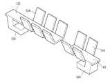
도 6은 도 4 및 도 5에 도시된 리드 프레임을 나타낸 사시도.
도 7은 제 3 실시예에 따른 발광 장치의 단면도.
도 8은 도 7에 도시된 리드 프레임을 나타낸 사시도.
도 9는 실시예에 따른 발광 장치가 구비된 표시 장치를 나타내는 사시도.1 is a front view of a light emitting device according to the first embodiment;
2 is a cross-sectional view along the X axis of FIG.
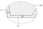
3 is an enlarged view of a portion of the lead frame and the substrate shown in FIG. 2;
4 is a front view of the light emitting device according to the second embodiment;
5 is a cross-sectional view along the X axis of FIG. 4.
6 is a perspective view of the lead frame shown in FIGS. 4 and 5.
7 is a sectional view of a light emitting device according to a third embodiment;
8 is a perspective view showing the lead frame shown in FIG.
9 is a perspective view illustrating a display device including a light emitting device according to an embodiment.
이하에서는, 본 실시예에 대하여 첨부되는 도면을 참조하여 상세하게 살펴보도록 한다. 다만, 본 실시예가 개시하는 사항으로부터 본 실시예가 갖는 발명의 사상의 범위가 정해질 수 있을 것이며, 본 실시예가 갖는 발명의 사상은 제안되는 실시예에 대하여 구성요소의 추가, 삭제, 변경 등의 실시변형을 포함한다고 할 것이다.Hereinafter, with reference to the accompanying drawings for the present embodiment will be described in detail. However, the scope of the inventive idea of the present embodiment may be determined from the matters disclosed by the present embodiment, and the inventive idea of the present embodiment may be implemented by adding, deleting, or modifying components to the proposed embodiment. It will be said to include variations.
도 1은 제 1 실시예에 따른 발광 장치의 정면도이고, 도 2는 도 1의 X축 단면도이며, 도 3은 도 2에 도시된 리드 프레임과 기판의 일부 영역 확대도이다.1 is a front view of the light emitting device according to the first embodiment, FIG. 2 is a cross-sectional view of the X-axis of FIG. 1, and FIG. 3 is an enlarged view of a portion of the lead frame and the substrate shown in FIG. 2.
발광 장치(100)는 측면 발광형 또는 상면 발광형 패키지 제품으로 직육면체 또는 정육면체 등과 같은 다각형 형상으로 형성될 수 있으며, 액정표시장치의 백라이트 광원, 조명 분야 등의 라이트 유닛으로 적용될 수 있다. 이하에서는 설명의 편의를 위하여 측면 발광형 발광 장치에 대해 설명하기로 한다.The
상기 발광 장치(100)는 캐비티(120)를 갖는 기판(110), 리드 프레임(133,143) 및 발광 소자(light emitting device)(150)를 포함한다.The
상기 기판(110)은 폴리프탈아미드(PPA), 폴리아미드9T(PA9T), 액정폴리머(LCP), 신지오택틱폴리스티렌(SPS) 중 어느 하나의 재질을 포함할 수 있다. 또한, 상기 기판(110)은 PCB가 될 수도 있다.The
상기 기판(110)의 상면에는 소정 깊이의 캐비티(120)를 포함한다. 다만, 실시예에 따라 상기 캐비티(120)는 형성되지 않을 수도 있다.The upper surface of the
여기서, 상기 기판(110)의 제 1 방향을 X축 방향이라 하고, 제 2 방향을 Y축 방향이라고 하며, X축 방향의 기판 길이는 Y축 방향의 기판 폭보다 길 수도 있으며, 이러한 기판의 형상에 한정되는 것은 아니다.Here, the first direction of the
상기 기판(110)의 상부에는 리드 프레임(133,143)이 사출 성형되며, 상기 리드 프레임(133,143)의 일부는 캐비티(120)로부터 노출된다.
상기 리드 프레임(133,143)은, 도 2에 도시된 바와 같이, 상기 기판(110) 내측 방향(Z축 하방향)으로 돌출형성되는 리드 프레임 돌출부(134,144)을 갖는다. 즉, 상기 발광 소자(150)로부터 발생되는 열의 방열이 우수해지도록 하기 위하여, 금속 재질로 이루어진 리드 프레임(133,143)에 방열 면적을 높이기 위한 리드 프레임 돌출부(134,144)가 형성된다.As shown in FIG. 2, the
그리고, 상기 리드 프레임 돌출부(134,144)는, 도 3에 도시되는 바와 같이, 상기 기판(110)까지의 거리를 고려하여 형성될 수 있다. 즉, 상기 리드 프레임 돌출부 중 제 1 리드 프레임 돌출부(134)는 상기 기판(110)의 측면부(111) 및/또는 기판의 바닥부(112)로부터 소정 거리 이상을 유지하도록 형성될 수 있다.The
예를 들면, 상기 제 1 리드 프레임 돌출부(134)는 상기 기판(110)의 측면부(111)와 바닥부(112)로부터 각각 50㎛ 내지 100㎛ 범위의 거리만큼 떨어지도록 형성될 수 있다. 만약, 간격이 50㎛ 이내가 될 경우에는, 외부(특히, 아래에서)로부터 상기 리드 프레임(133,143)측으로 수분이 침투될 가능성이 높기 때문이다.For example, the first
상기 제 1 리드 프레임 돌출부(134)가 기판 측면부(111)로부터 떨어진 거리를 A라고 하고, 기판 바닥부(112)로부터 떨어진 거리를 B라고 할 경우에, A와 B 모두 50㎛ 이상의 거리가 되도록 하는 것이 유리하다.When the distance from the substrate side portion 111 of the first
상기 리드 프레임(133,143) 및 리드 프레임 돌출부(134,144)은 동일한 금속 재질로 일체로 형성될 수 있으며, 그 재료로는 철(Fe), 주석(Sn), 크롬(Cr), 아연(Zn), 니켈(Ni), 알루미늄, 은, 금, 구리 및 이들의 합금 형태로 이루어진 금속 중에서 어느 하나로 사출성형될 수 있다.The
상기 캐비티(120)의 X축 방향의 좌/우 측면(131)과, 상하 측면(132)은 기판 일부로서, 소정 각도 경사지게 형성될 수 있으며, 이 경우, 도 1에 도시되는 바와 같이, 그 경사진 형상이 보여진다.The left and
상기 발광 소자(150)는 캐비티(120)에 배치된 적어도 한 리드 프레임(133,143)에 장착되고, 와이어(152)로 상기 리드 프레임(133,143)에 연결된다. 또한, 상기 발광 소자(150)는 복수 개의 리드 프레임(133,143)에 와이어 본딩(wire bonding), 플립 본딩(flip bonding), 다이 본딩(die bonding) 등의 방식으로 탑재될 수 있다. 그리고, 상기 발광 소자(150)는 상기 기판(110) 상에 설치되어 상기 리드 프레임(133,143)과 전기적으로 연결될 수도 있다.The
또한, 상기 발광 소자(150)는 3족 원소와 5족 원소의 화합물 반도체로서, AlGaN 계열, GaN 계열, InGaAlP 계열, GaAs 계열의 LED 칩 중 어느 하나를 하나 이상 포함할 수 있다. 또한 발광 소자(150)의 보호를 위해 제너 다이오드와 같은 보호 소자가 탑재될 수도 있다.In addition, the
한편, 상기 발광 장치(100)는 구현하는 형태에 따라 청색 LED 칩과 황색 형광체(예: 실리케이트계 형광체), 오렌지 형광체, 그린 형광체, 적색 형광체를 이용한 백색 발광 소자로 구현할 수 있다. 또한 적색 LED 칩, 녹색 LED 칩, 청색 LED 칩, 엘로우 LED 칩, 엘로우 그린(Yellow green) LED 칩, UV LED 칩 중 적어도 하나 또는 그 이상을 조합하여 광원으로 구현할 수도 있다.The
그리고, 상기 캐비티(120)에는 발광 소자(150)를 보호하기 위해 수지물이 몰딩되며, 상기 수지물은 투명한 재질의 에폭시 또는 실리콘 등을 이용할 수 있으며, 필요에 따라 형광체 분말이 첨가되어 몰딩된다. 상기 수지물은 몰딩액 또는 첨가물을 사용 목적, 사용 환경, 제품의 특성에 따라 선택적으로 사용할 수 있다. 또한, 상기 수지물의 표면은 플랫 형태, 오목 렌즈 형태, 볼록 렌즈 형태 중 어느 한 형태로 형성될 수 있다.In addition, a resin material is molded in the
도 4는 제 2 실시예에 따른 발광 장치의 정면도이고, 도 5는 도 1의 X축 단면도이며, 도 6은 도 4 및 도 5에 도시된 리드 프레임을 나타낸 사시도이다. 앞선 제 1 실시예와 동일한 구성에 대해서는 그 설명을 생략하기로 한다.4 is a front view of the light emitting device according to the second embodiment, FIG. 5 is a sectional view along the X axis of FIG. 1, and FIG. 6 is a perspective view showing the lead frame shown in FIGS. 4 and 5. The same configuration as that of the first embodiment will be omitted.
제 2 실시예의 발광 장치(100)는 상기 발광 장치(100)는 캐비티(120)를 갖는 기판(110), 리드 프레임(133,143) 및 발광 소자(light emitting device)(150)를 포함한다. 상기 기판(110)은 PCB가 될 수도 있다.In the
제 2 실시예의 리드 프레임(133,143)은, 도 5에 도시된 바와 같이, 상기 캐비티(120) 방향(Z축 상방향)으로 돌출형성되는 리드 프레임 돌출부(234,244)를 갖는다. 즉, 상기 발광 소자(150)로부터 발생되는 열의 방열이 우수해지도록 하기 위하여, 금속 재질로 이루어진 리드 프레임(133,143)에 방열 면적을 높이기 위한 리드 프레임 돌출부(234,244)가 형성되며, 도 4에 도시된 바와 같이, 상기 기판(110)의 캐비티(120) 주변에 배열된다.As shown in FIG. 5, the
그리고, 상기 리드 프레임 돌출부(234,244)는, 도 6에 도시되는 바와 같이, 복수 개의 돌출부들로 이루어질 수 있다. 그리고, 상기 기판(110) 캐비티(120)의 경사진 면을 따라 형성될 수 있도록, 상기 리드 프레임(133,143)으로부터 수직으로 돌출되는 것이 아니라 소정 각도 경사지게 형성될 수 있다.The
도 6에는, 제 1 리드 프레임(133)으로부터 상측 방향으로 돌출 형성되는 제 1 리드 프레임 돌출부(234)와, 제 2 리드 프레임(143)으로부터 상측 방향으로 돌출 형성되는 제 2 리드 프레임 돌출부(244)가 도시되어 있으며, 상기 제 1 리드 프레임 돌출부(234)는 6개, 제 2 리드 프레임 돌출부(244)는 4개 도시된다.6, a first
다만, 이러한 개수 및 리드 프레임 돌출부의 형상에 대해서는 하나의 예에 불과하며, 다양한 실시예의 변경에 따라 제 1 실시예와 같이 몸통 형상을 갖는 돌출부가 리드 프레임으로부터 상측방향으로 돌출형성되는 것도 가능하며, 그 개수 역시 다양하게 변경할 수 있다.However, the number and shape of the lead frame protrusions are just one example, and according to the change of various embodiments, protrusions having a body shape as in the first embodiment may protrude upward from the lead frame. The number can also vary.
이러한 리드 프레임 돌출부(234,244)는 도 4에서와 같이 기판(110)의 캐비티(120) 영역 외측에 형성될 수 있으며, 그 실시예의 변경에 따라, 상기 캐비티(120)내의 경사면을 따라 형성되는 것도 가능하다.The
상기 리드 프레임(133,143) 및 리드 프레임 돌출부(234,244)은 동일한 금속 재질로 일체로 형성될 수 있으며, 그 재료로는, 앞서 설명한 바와 같이, 철(Fe), 주석(Sn), 크롬(Cr), 아연(Zn), 니켈(Ni), 알루미늄, 은, 금, 구리 및 이들의 합금 형태로 이루어진 금속 중에서 어느 하나로 사출성형될 수 있으며, 상기 기판(110) 성형시 캐비티(120)와 함께 형성될 수 있다.The lead frames 133 and 143 and the
도 7은 제 3 실시예에 따른 발광 장치의 단면도이고, 도 8 도 7에 도시된 리드 프레임을 나타낸 사시도이다. 앞선 제 1 실시예 및 제 2 실시예와 동일한 구성에 대해서는 그 설명을 생략하기로 한다.7 is a cross-sectional view of the light emitting device according to the third embodiment, and is a perspective view showing the lead frame shown in FIG. 8. The same configuration as that of the first and second embodiments will be omitted.
도 7 및 도 8에 도시되는 제 3 실시예의 발광 장치 역시 리드 프레임(133,143)이 돌출부를 갖는 것이며, 상기 리드 프레임(133,143)으로부터 연장되어 돌출되는 리드 프레임 돌출부는 상측 방향으로 돌출되는 돌출부와, 하측 방향으로 돌출되는 돌출부를 갖는다.In the light emitting device of the third embodiment shown in FIGS. 7 and 8, the lead frames 133 and 143 have protrusions, and the lead frame protrusions extending from the lead frames 133 and 143 protrude upward, and the lower side protrudes. It has a protrusion projecting in the direction.
즉, 상기 리드 프레임(133,143)으로부터 연장되는 돌출부는, 리드 프레임으로부터 기판(110)의 캐비티(120) 방향(Z축 상방향)으로 돌출되는 제 1 리드 프레임 돌출부(334,344)와, 리드 프레임으로부터 기판(110) 내측 방향(Z축 하방향)으로 돌출되는 제 2 리드 프레임 돌출부(335,345)를 포함할 수 있다. 여기서, 상기 제 1 리드 프레임 돌출부는 기판에 대하여 상측 방향으로 돌출되므로, 리드 프레임 상측 돌출부라고 하고, 상기 제 2 리드 프레임 돌출부는 기판에 대하여 하측 방향으로 돌출되므로 리드 프레임 하측 돌출부라고도 할 수 있다.That is, the protrusions extending from the lead frames 133 and 143 may include first
다만, 이하의 설명에서는, 본 발명의 구성요소를 보다 쉽게 이해하기 위하여 제 1 리드 프레임 돌출부를 리드 프레임 상측 돌출부라고 하고, 제 2 리드 프레임 돌출부를 리드 프레임 하측 돌출부라고 하기로 한다.However, in the following description, in order to more easily understand the components of the present invention, the first lead frame protrusion is referred to as the lead frame upper protrusion, and the second lead frame protrusion is referred to as the lead frame lower protrusion.
상기 리드 프레임 상측 돌출부(334,344)는, 앞선 제 2 실시예의 경우와 같이, 복수 개의 돌출부들이 소정 각도 경사진 각도로 캐비티(120) 외측 둘레에 배열될 수 있다.The lead frame
그리고, 상기 리드 프레임 하측 돌출부(335,345)는 L자 형상으로 그 일부가 기판(110) 내부에 위치하도록 형성될 수 있으며, 방열 면적을 더 넓게 하기 위하여, 제 1 실시예의 경우와 같은 몸통 형상으로 제공될 수도 있다.In addition, the lead frame
이러한 제 3 실시예에 의한 리드 프레임 돌출부는, 상기 발광 소자(150)에서 발생되는 열이 상측 방향 뿐만 아니라 하측 방향으로 방열될 수 있도록 하므로, 그 방열 특성이 좀 더 우수할 수 있다.The lead frame protrusion according to the third embodiment allows heat generated in the
상기 리드 프레임(133,143) 및 리드 프레임 돌출부(334,344,335,345)은 동일한 금속 재질로 일체로 형성될 수 있으며, 그 재료로는, 앞서 설명한 바와 같이, 철(Fe), 주석(Sn), 크롬(Cr), 아연(Zn), 니켈(Ni), 알루미늄, 은, 금, 구리 및 이들의 합금 형태로 이루어진 금속 중에서 어느 하나로 사출성형될 수 있다.The lead frames 133 and 143 and the
도 9는 실시예에 따른 발광 장치가 구비된 표시 장치를 나타내는 사시도이다.9 is a perspective view illustrating a display device including a light emitting device according to an embodiment.
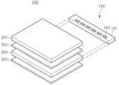
도 9를 참조하면, 표시장치(200)는 발광 장치(100)를 포함하는 발광 모듈(104), 반사 플레이트(201), 광 가이드플레이트(203), 광학 시트(205) 및 표시 패널(207)을 포함한다.Referring to FIG. 9, the
상기 발광 모듈(104)은 복수 개의 발광 장치(100)가 기판(102)에 탑재되는 구조이다. 상기 발광 장치(100)는 도 1 내지 도 3에 도시된 바와 같은 제 1 실시예의 패키지이거나, 도 4 내지 도 6에 도시된 제 2 실시예의 패키지이거나, 도 7 및 도 8에 도시된 제 3 실시예의 패키지이거나, 이들의 조합 또는 이들로부터 알 수 있는 다른 변형례의 패키지가 될 수 있다.The
이러한 발광 모듈(104)은 광 가이드 플레이트(203)의 적어도 한 측면에 대응되며, 발광된 광은 상기 광 가이드 플레이트(203)의 측면으로 입사된다.The
상기 광 가이드 플레이트(203)는 입사된 광을 전 영역으로 가이드하여, 면 광원으로 방출되게 한다. 또한, 상기 광 가이드 플레이트(203)의 어느 한면은 반사 패턴이 형성될 수 있다.The
상기 반사 플레이트(201)는 광 가이드 플레이트(203)의 아래에 배치되며, 상기 광 가이드 플레이트(203)로부터 아래로 누설되는 광을 반사시켜 준다.The
상기 광 가이드 플레이트(203)로부터 방출된 광은 광학 시트(205)를 통해 표시 패널(207)로 조사된다. 여기서, 상기 광학 시트(205)는 확산 시트, 프리즘 시트 중 적어도 한장을 포함할 수 있다. 상기 확산 시트는 광 가이드 플레이트(203) 위에 배치되며, 입사되는 광을 확산시켜 준다. 그리고, 상기 프리즘 시트는 상기 확산 시트 위에 배치될 수 있으며, 확산되는 광을 표시 영역으로 집광시켜 준다.Light emitted from the
여기서, 발광 모듈(104), 광 가이드 플레이트(203), 광학 시트(205)는 라이트 유닛으로 정의될 수 있으며, 상기 라이트 유닛은 반사 플레이트(201)를 포함할 수 있다. 또한, 상기 라이트 유닛의 구성 요소 일부는 도시하지 않은 몰드 프레임, 샤시 구조물, 금속 바텀 커버 등과 같은 구조물에 수납될 수 있다.The
상기 표시 패널(207)은 액정 패널로서, 두 개의 투명한 기판과 액정을 포함하며, 투과되는 광과 액정 구동에 의해 정보를 표시할 수 있다. 이러한 표시 패널(207)에 대해서는 한정하지 않으며, 변경될 수 있다. 또한, 광 가이드 플레이트(203)의 양측으로 표시 패널이 배치될 수 있다.The
이러한 표시 장치(200)는 핸드폰, PMP 등의 휴대 단말기나 컴퓨터에 적용될 수 있다.The
이상에서는 실시 예를 중심으로 설명하였으나, 이는 단지 예시일 뿐 본 발명을 한정하는 것이 아니며, 본 발명이 속하는 분야의 통상의 지식을 가진 자라면 본 발명의 본질적인 특성을 벗어나지 않는 범위에서 이상에 예시되지 않은 여러 가지의 변형과 응용이 가능함을 알 수 있을 것이다. 예를 들어, 본 발명의 실시예에 구체적으로 나타난 각 구성 요소는 변형하여 실시할 수 있는 것이다. 그리고 이러한 변형과 응용에 관계된 차이점들은 첨부된 청구 범위에서 규정하는 본 발명의 범위에 포함되는 것으로 해석되어야 할 것이다.Although the above description has been made with reference to the embodiments, these are merely examples and are not intended to limit the present invention. Those skilled in the art to which the present invention pertains should not be exemplified above without departing from the essential characteristics of the present invention. It will be understood that various modifications and applications are possible. For example, each component specifically shown in the embodiments of the present invention can be modified and implemented. And differences relating to such modifications and applications will have to be construed as being included in the scope of the invention defined in the appended claims.
Claims (14)
Translated fromKorean상기 캐비티에 배치되며, 제1 리드 프레임과 상기 제1 리드 프레임과 전기적으로 절연된 제2 리드 프레임을 포함하는 리드 프레임;
상기 제1 리드 프레임에 배치된 발광 소자;
상기 발광 소자와 상기 제2 리드 프레임을 전기적으로 연결하는 와이어;
를 포함하고,
상기 리드 프레임은 상기 제1 리드 프레임에서 하부 방향으로 돌출된 제1 리드 프레임 돌출부, 상기 제2 리드 프레임에서 하부 방향으로 돌출된 제2 리드 프레임 돌출부, 및 상기 제1 리드 프레임과 상기 제2 리드 프레임 중 적어도 하나에서 상부 방향으로 돌출된 제3 리드 프레임 돌출부를 포함하는 발광 장치.A substrate comprising a cavity;
A lead frame disposed in the cavity and including a first lead frame and a second lead frame electrically insulated from the first lead frame;
A light emitting element disposed on the first lead frame;
A wire electrically connecting the light emitting element and the second lead frame;
Including,
The lead frame may include a first lead frame protrusion protruding downward from the first lead frame, a second lead frame protrusion protruding downward from the second lead frame, and the first lead frame and the second lead frame. And a third lead frame protrusion protruding in an upward direction in at least one of the light emitting devices.
상기 기판 상에 배치되는 발광 소자; 및
상기 발광 소자와 전기적으로 연결되는 리드 프레임;을 포함하고,
상기 리드 프레임은 베이스 프레임과, 상기 베이스 프레임에서 상측 방향으로 돌출되는 제 1 리드 프레임 돌출부와, 상기 베이스 프레임에서 상기 기판 외부로 노출되어 하측 방향으로 연장된 연장부와 상기 연장부로부터 절곡되어 상기 기판 내부에 삽입된 삽입부를 갖는 제2 리드 프레임 돌출부를 포함하고,
상기 연장부 및 상기 삽입부의 두께는 상기 베이스 프레임의 두께에 비하여 더 두꺼운 발광 장치.Board;
A light emitting element disposed on the substrate; And
And a lead frame electrically connected to the light emitting device.
The lead frame may include a base frame, a first lead frame protrusion protruding upward from the base frame, an extension part exposed from the base frame to the outside of the substrate and extending downward, and bent from the extension part. A second lead frame protrusion having an insertion portion inserted therein,
The thickness of the extension portion and the insertion portion is thicker than the thickness of the base frame.
상기 제 1 리드 프레임 돌출부는 상기 리드 프레임으로부터 상측 방향으로 연장되는 복수 개의 돌출부들을 포함하는 발광 장치.The method of claim 9,
The first lead frame protrusion includes a plurality of protrusions extending upward from the lead frame.
상기 제 2 리드 프레임 돌출부는 L자 형상으로 형성된 발광 장치.The method of claim 9,
The light emitting device of claim 2, wherein the second lead frame protrusion is formed in an L shape.
상기 발광 모듈의 일측에 배치되는 광 가이드 플레이트;
를 포함하는 라이트 유닛.A light emitting module comprising the light emitting device according to any one of claims 1 to 4 and 8 to 11;
A light guide plate disposed on one side of the light emitting module;
Light unit comprising a.
Priority Applications (4)
| Application Number | Priority Date | Filing Date | Title |
|---|---|---|---|
| KR1020100029941AKR101047676B1 (en) | 2010-04-01 | 2010-04-01 | Light emitting device and light unit having same |
| EP11160354.4AEP2372794B1 (en) | 2010-04-01 | 2011-03-30 | Lighting device, display device and lighting system having the same |
| US13/075,405US9076942B2 (en) | 2010-04-01 | 2011-03-30 | Lighting device and lighting system having the same |
| CN201110086632.0ACN102213373B (en) | 2010-04-01 | 2011-04-01 | Lighting device, display device and lighting system having the same |
Applications Claiming Priority (1)
| Application Number | Priority Date | Filing Date | Title |
|---|---|---|---|
| KR1020100029941AKR101047676B1 (en) | 2010-04-01 | 2010-04-01 | Light emitting device and light unit having same |
Publications (1)
| Publication Number | Publication Date |
|---|---|
| KR101047676B1true KR101047676B1 (en) | 2011-07-08 |
Family
ID=44168416
Family Applications (1)
| Application Number | Title | Priority Date | Filing Date |
|---|---|---|---|
| KR1020100029941AExpired - Fee RelatedKR101047676B1 (en) | 2010-04-01 | 2010-04-01 | Light emitting device and light unit having same |
Country Status (4)
| Country | Link |
|---|---|
| US (1) | US9076942B2 (en) |
| EP (1) | EP2372794B1 (en) |
| KR (1) | KR101047676B1 (en) |
| CN (1) | CN102213373B (en) |
Families Citing this family (1)
| Publication number | Priority date | Publication date | Assignee | Title |
|---|---|---|---|---|
| KR20120093679A (en)* | 2011-02-15 | 2012-08-23 | 삼성전자주식회사 | Light emitting device package and manufacturing method thereof |
Citations (2)
| Publication number | Priority date | Publication date | Assignee | Title |
|---|---|---|---|---|
| JP2007142044A (en)* | 2005-11-16 | 2007-06-07 | Stanley Electric Co Ltd | Semiconductor light emitting device and surface light source using the same |
| JP2008300386A (en)* | 2007-05-29 | 2008-12-11 | Iwatani Internatl Corp | Semiconductor light emitting device |
Family Cites Families (16)
| Publication number | Priority date | Publication date | Assignee | Title |
|---|---|---|---|---|
| JP2003152228A (en) | 2001-11-12 | 2003-05-23 | Sumitomo Bakelite Co Ltd | Led case and led light emitting body |
| JP2004146815A (en)* | 2002-09-30 | 2004-05-20 | Sanyo Electric Co Ltd | Light emitting device |
| JP3910171B2 (en) | 2003-02-18 | 2007-04-25 | シャープ株式会社 | Semiconductor light emitting device, method for manufacturing the same, and electronic imaging device |
| JP2005116937A (en) | 2003-10-10 | 2005-04-28 | Matsushita Electric Ind Co Ltd | Semiconductor light emitting device and manufacturing method thereof |
| JP2007012727A (en)* | 2005-06-29 | 2007-01-18 | Toyoda Gosei Co Ltd | Light emitting device |
| JP2007184534A (en) | 2005-12-09 | 2007-07-19 | Matsushita Electric Ind Co Ltd | LIGHT EMITTING MODULE, ITS MANUFACTURING METHOD, AND BACKLIGHT DEVICE USING THE SAME |
| KR101224376B1 (en) | 2006-01-25 | 2013-01-21 | 삼성디스플레이 주식회사 | Backlight assembly and liquid crystal display apparatus having the same |
| JP2007329152A (en)* | 2006-06-06 | 2007-12-20 | Matsushita Electric Ind Co Ltd | Glass, glass manufacturing method, semiconductor light emitting device, and semiconductor light emitting device manufacturing method |
| JP2008016744A (en)* | 2006-07-10 | 2008-01-24 | Matsushita Electric Ind Co Ltd | Package for semiconductor light emitting device and method for manufacturing the same |
| KR100772433B1 (en)* | 2006-08-23 | 2007-11-01 | 서울반도체 주식회사 | LED package adopting lead terminal with reflecting surface |
| KR20090003740U (en)* | 2007-10-17 | 2009-04-22 | 엘지이노텍 주식회사 | LED Package |
| JP5186930B2 (en)* | 2008-01-24 | 2013-04-24 | 豊田合成株式会社 | Light emitting device |
| KR100986202B1 (en)* | 2008-07-01 | 2010-10-07 | 알티전자 주식회사 | Side view light emitting diode package |
| JP2010021259A (en)* | 2008-07-09 | 2010-01-28 | Toshiba Corp | Optical semiconductor device |
| US8288785B2 (en)* | 2008-12-03 | 2012-10-16 | Seoul Semiconductor Co., Ltd. | Lead frame having light-reflecting layer, light emitting diode having the lead frame, and backlight unit having the light emitting diode |
| CN201344485Y (en) | 2008-12-12 | 2009-11-11 | 张宇 | LED polyhedral lamp |
- 2010
- 2010-04-01KRKR1020100029941Apatent/KR101047676B1/ennot_activeExpired - Fee Related
- 2011
- 2011-03-30EPEP11160354.4Apatent/EP2372794B1/enactiveActive
- 2011-03-30USUS13/075,405patent/US9076942B2/enactiveActive
- 2011-04-01CNCN201110086632.0Apatent/CN102213373B/enactiveActive
Patent Citations (2)
| Publication number | Priority date | Publication date | Assignee | Title |
|---|---|---|---|---|
| JP2007142044A (en)* | 2005-11-16 | 2007-06-07 | Stanley Electric Co Ltd | Semiconductor light emitting device and surface light source using the same |
| JP2008300386A (en)* | 2007-05-29 | 2008-12-11 | Iwatani Internatl Corp | Semiconductor light emitting device |
Also Published As
| Publication number | Publication date |
|---|---|
| US20110242825A1 (en) | 2011-10-06 |
| US9076942B2 (en) | 2015-07-07 |
| EP2372794A2 (en) | 2011-10-05 |
| CN102213373A (en) | 2011-10-12 |
| EP2372794A3 (en) | 2015-12-23 |
| CN102213373B (en) | 2015-07-01 |
| EP2372794B1 (en) | 2019-11-20 |
Similar Documents
| Publication | Publication Date | Title |
|---|---|---|
| JP3175433U (en) | Semiconductor diode package | |
| CN102157504B (en) | Light emitting diode package and light unit having the same | |
| KR100818518B1 (en) | LED Package | |
| US8783933B2 (en) | Light emitting device package, and display apparatus and lighting system having the same | |
| KR101047676B1 (en) | Light emitting device and light unit having same | |
| KR20130024152A (en) | Light unit and display device | |
| KR101327124B1 (en) | Lighting Emitting Apparatus | |
| KR101923688B1 (en) | Light emitting device package and light unit | |
| KR101683887B1 (en) | Light emitting device package and light unit having thereof | |
| KR20090064717A (en) | Light emitting diode package | |
| KR102119746B1 (en) | Light emitting device and light emitting device package | |
| KR101878863B1 (en) | The light emitting device package and the light emitting system | |
| KR20090003740U (en) | LED Package | |
| KR20130028289A (en) | Light emitting device package and light unit | |
| KR20140145402A (en) | Light unit | |
| KR20100003324A (en) | Light-emitting device | |
| KR20130119132A (en) | Light emitting device, lightr emitting module and lighting system | |
| KR20130083173A (en) | The light emitting device package and the light emitting system | |
| KR20180129714A (en) | Light emitting device package and light unit | |
| KR20100082393A (en) | Light emitting device package | |
| KR20140099683A (en) | Light Emitting Devices package |
Legal Events
| Date | Code | Title | Description |
|---|---|---|---|
| PA0109 | Patent application | St.27 status event code:A-0-1-A10-A12-nap-PA0109 | |
| A201 | Request for examination | ||
| A302 | Request for accelerated examination | ||
| PA0201 | Request for examination | St.27 status event code:A-1-2-D10-D11-exm-PA0201 | |
| PA0302 | Request for accelerated examination | St.27 status event code:A-1-2-D10-D17-exm-PA0302 St.27 status event code:A-1-2-D10-D16-exm-PA0302 | |
| D13-X000 | Search requested | St.27 status event code:A-1-2-D10-D13-srh-X000 | |
| D14-X000 | Search report completed | St.27 status event code:A-1-2-D10-D14-srh-X000 | |
| E13-X000 | Pre-grant limitation requested | St.27 status event code:A-2-3-E10-E13-lim-X000 | |
| P11-X000 | Amendment of application requested | St.27 status event code:A-2-2-P10-P11-nap-X000 | |
| P13-X000 | Application amended | St.27 status event code:A-2-2-P10-P13-nap-X000 | |
| E902 | Notification of reason for refusal | ||
| PE0902 | Notice of grounds for rejection | St.27 status event code:A-1-2-D10-D21-exm-PE0902 | |
| E13-X000 | Pre-grant limitation requested | St.27 status event code:A-2-3-E10-E13-lim-X000 | |
| P11-X000 | Amendment of application requested | St.27 status event code:A-2-2-P10-P11-nap-X000 | |
| P13-X000 | Application amended | St.27 status event code:A-2-2-P10-P13-nap-X000 | |
| E701 | Decision to grant or registration of patent right | ||
| PE0701 | Decision of registration | St.27 status event code:A-1-2-D10-D22-exm-PE0701 | |
| GRNT | Written decision to grant | ||
| PR0701 | Registration of establishment | St.27 status event code:A-2-4-F10-F11-exm-PR0701 | |
| PR1002 | Payment of registration fee | St.27 status event code:A-2-2-U10-U11-oth-PR1002 Fee payment year number:1 | |
| PG1601 | Publication of registration | St.27 status event code:A-4-4-Q10-Q13-nap-PG1601 | |
| FPAY | Annual fee payment | Payment date:20140609 Year of fee payment:4 | |
| PR1001 | Payment of annual fee | St.27 status event code:A-4-4-U10-U11-oth-PR1001 Fee payment year number:4 | |
| PN2301 | Change of applicant | St.27 status event code:A-5-5-R10-R13-asn-PN2301 St.27 status event code:A-5-5-R10-R11-asn-PN2301 | |
| FPAY | Annual fee payment | Payment date:20150605 Year of fee payment:5 | |
| PR1001 | Payment of annual fee | St.27 status event code:A-4-4-U10-U11-oth-PR1001 Fee payment year number:5 | |
| FPAY | Annual fee payment | Payment date:20160607 Year of fee payment:6 | |
| PR1001 | Payment of annual fee | St.27 status event code:A-4-4-U10-U11-oth-PR1001 Fee payment year number:6 | |
| R18-X000 | Changes to party contact information recorded | St.27 status event code:A-5-5-R10-R18-oth-X000 | |
| FPAY | Annual fee payment | Payment date:20170605 Year of fee payment:7 | |
| PR1001 | Payment of annual fee | St.27 status event code:A-4-4-U10-U11-oth-PR1001 Fee payment year number:7 | |
| PR1001 | Payment of annual fee | St.27 status event code:A-4-4-U10-U11-oth-PR1001 Fee payment year number:8 | |
| R18-X000 | Changes to party contact information recorded | St.27 status event code:A-5-5-R10-R18-oth-X000 | |
| FPAY | Annual fee payment | Payment date:20190612 Year of fee payment:9 | |
| PR1001 | Payment of annual fee | St.27 status event code:A-4-4-U10-U11-oth-PR1001 Fee payment year number:9 | |
| R18-X000 | Changes to party contact information recorded | St.27 status event code:A-5-5-R10-R18-oth-X000 | |
| PR1001 | Payment of annual fee | St.27 status event code:A-4-4-U10-U11-oth-PR1001 Fee payment year number:10 | |
| PN2301 | Change of applicant | St.27 status event code:A-5-5-R10-R13-asn-PN2301 St.27 status event code:A-5-5-R10-R11-asn-PN2301 | |
| PR1001 | Payment of annual fee | St.27 status event code:A-4-4-U10-U11-oth-PR1001 Fee payment year number:11 | |
| PN2301 | Change of applicant | St.27 status event code:A-5-5-R10-R11-asn-PN2301 | |
| PN2301 | Change of applicant | St.27 status event code:A-5-5-R10-R14-asn-PN2301 | |
| PR1001 | Payment of annual fee | St.27 status event code:A-4-4-U10-U11-oth-PR1001 Fee payment year number:12 | |
| PR1001 | Payment of annual fee | St.27 status event code:A-4-4-U10-U11-oth-PR1001 Fee payment year number:13 | |
| PC1903 | Unpaid annual fee | St.27 status event code:A-4-4-U10-U13-oth-PC1903 Not in force date:20240702 Payment event data comment text:Termination Category : DEFAULT_OF_REGISTRATION_FEE | |
| P22-X000 | Classification modified | St.27 status event code:A-4-4-P10-P22-nap-X000 | |
| PC1903 | Unpaid annual fee | St.27 status event code:N-4-6-H10-H13-oth-PC1903 Ip right cessation event data comment text:Termination Category : DEFAULT_OF_REGISTRATION_FEE Not in force date:20240702 |