KR101047652B1 - Light emitting device and manufacturing method - Google Patents
Light emitting device and manufacturing methodDownload PDFInfo
- Publication number
- KR101047652B1 KR101047652B1KR1020090127189AKR20090127189AKR101047652B1KR 101047652 B1KR101047652 B1KR 101047652B1KR 1020090127189 AKR1020090127189 AKR 1020090127189AKR 20090127189 AKR20090127189 AKR 20090127189AKR 101047652 B1KR101047652 B1KR 101047652B1
- Authority
- KR
- South Korea
- Prior art keywords
- light emitting
- gallium
- aluminum
- oxide
- gallium aluminum
- Prior art date
- Legal status (The legal status is an assumption and is not a legal conclusion. Google has not performed a legal analysis and makes no representation as to the accuracy of the status listed.)
- Expired - Fee Related
Links
Images


Classifications
- H—ELECTRICITY
- H01—ELECTRIC ELEMENTS
- H01L—SEMICONDUCTOR DEVICES NOT COVERED BY CLASS H10
- H01L21/00—Processes or apparatus adapted for the manufacture or treatment of semiconductor or solid state devices or of parts thereof
- H01L21/02—Manufacture or treatment of semiconductor devices or of parts thereof
- H01L21/04—Manufacture or treatment of semiconductor devices or of parts thereof the devices having potential barriers, e.g. a PN junction, depletion layer or carrier concentration layer
- H01L21/18—Manufacture or treatment of semiconductor devices or of parts thereof the devices having potential barriers, e.g. a PN junction, depletion layer or carrier concentration layer the devices having semiconductor bodies comprising elements of Group IV of the Periodic Table or AIIIBV compounds with or without impurities, e.g. doping materials
- H01L21/20—Deposition of semiconductor materials on a substrate, e.g. epitaxial growth solid phase epitaxy
- H—ELECTRICITY
- H10—SEMICONDUCTOR DEVICES; ELECTRIC SOLID-STATE DEVICES NOT OTHERWISE PROVIDED FOR
- H10H—INORGANIC LIGHT-EMITTING SEMICONDUCTOR DEVICES HAVING POTENTIAL BARRIERS
- H10H20/00—Individual inorganic light-emitting semiconductor devices having potential barriers, e.g. light-emitting diodes [LED]
- H10H20/80—Constructional details
- H10H20/81—Bodies
- H10H20/822—Materials of the light-emitting regions
- H10H20/824—Materials of the light-emitting regions comprising only Group III-V materials, e.g. GaP
- H10H20/825—Materials of the light-emitting regions comprising only Group III-V materials, e.g. GaP containing nitrogen, e.g. GaN
- H—ELECTRICITY
- H01—ELECTRIC ELEMENTS
- H01L—SEMICONDUCTOR DEVICES NOT COVERED BY CLASS H10
- H01L21/00—Processes or apparatus adapted for the manufacture or treatment of semiconductor or solid state devices or of parts thereof
- H01L21/02—Manufacture or treatment of semiconductor devices or of parts thereof
- H01L21/02104—Forming layers
- H01L21/02365—Forming inorganic semiconducting materials on a substrate
- H01L21/02367—Substrates
- H01L21/0237—Materials
- H01L21/0242—Crystalline insulating materials
- H—ELECTRICITY
- H01—ELECTRIC ELEMENTS
- H01L—SEMICONDUCTOR DEVICES NOT COVERED BY CLASS H10
- H01L21/00—Processes or apparatus adapted for the manufacture or treatment of semiconductor or solid state devices or of parts thereof
- H01L21/02—Manufacture or treatment of semiconductor devices or of parts thereof
- H01L21/02104—Forming layers
- H01L21/02365—Forming inorganic semiconducting materials on a substrate
- H01L21/02436—Intermediate layers between substrates and deposited layers
- H01L21/02439—Materials
- H01L21/02455—Group 13/15 materials
- H01L21/02458—Nitrides
- H—ELECTRICITY
- H01—ELECTRIC ELEMENTS
- H01L—SEMICONDUCTOR DEVICES NOT COVERED BY CLASS H10
- H01L21/00—Processes or apparatus adapted for the manufacture or treatment of semiconductor or solid state devices or of parts thereof
- H01L21/02—Manufacture or treatment of semiconductor devices or of parts thereof
- H01L21/02104—Forming layers
- H01L21/02365—Forming inorganic semiconducting materials on a substrate
- H01L21/02436—Intermediate layers between substrates and deposited layers
- H01L21/02439—Materials
- H01L21/02488—Insulating materials
- H—ELECTRICITY
- H01—ELECTRIC ELEMENTS
- H01L—SEMICONDUCTOR DEVICES NOT COVERED BY CLASS H10
- H01L21/00—Processes or apparatus adapted for the manufacture or treatment of semiconductor or solid state devices or of parts thereof
- H01L21/02—Manufacture or treatment of semiconductor devices or of parts thereof
- H01L21/02104—Forming layers
- H01L21/02365—Forming inorganic semiconducting materials on a substrate
- H01L21/02436—Intermediate layers between substrates and deposited layers
- H01L21/02494—Structure
- H01L21/02496—Layer structure
- H01L21/02502—Layer structure consisting of two layers
- H—ELECTRICITY
- H01—ELECTRIC ELEMENTS
- H01L—SEMICONDUCTOR DEVICES NOT COVERED BY CLASS H10
- H01L21/00—Processes or apparatus adapted for the manufacture or treatment of semiconductor or solid state devices or of parts thereof
- H01L21/02—Manufacture or treatment of semiconductor devices or of parts thereof
- H01L21/02104—Forming layers
- H01L21/02365—Forming inorganic semiconducting materials on a substrate
- H01L21/02518—Deposited layers
- H01L21/02521—Materials
- H01L21/02538—Group 13/15 materials
- H01L21/0254—Nitrides
- H—ELECTRICITY
- H10—SEMICONDUCTOR DEVICES; ELECTRIC SOLID-STATE DEVICES NOT OTHERWISE PROVIDED FOR
- H10H—INORGANIC LIGHT-EMITTING SEMICONDUCTOR DEVICES HAVING POTENTIAL BARRIERS
- H10H20/00—Individual inorganic light-emitting semiconductor devices having potential barriers, e.g. light-emitting diodes [LED]
- H10H20/01—Manufacture or treatment
- H10H20/011—Manufacture or treatment of bodies, e.g. forming semiconductor layers
- H10H20/013—Manufacture or treatment of bodies, e.g. forming semiconductor layers having light-emitting regions comprising only Group III-V materials
- H10H20/0133—Manufacture or treatment of bodies, e.g. forming semiconductor layers having light-emitting regions comprising only Group III-V materials with a substrate not being Group III-V materials
- H10H20/01335—Manufacture or treatment of bodies, e.g. forming semiconductor layers having light-emitting regions comprising only Group III-V materials with a substrate not being Group III-V materials the light-emitting regions comprising nitride materials
- H—ELECTRICITY
- H10—SEMICONDUCTOR DEVICES; ELECTRIC SOLID-STATE DEVICES NOT OTHERWISE PROVIDED FOR
- H10H—INORGANIC LIGHT-EMITTING SEMICONDUCTOR DEVICES HAVING POTENTIAL BARRIERS
- H10H20/00—Individual inorganic light-emitting semiconductor devices having potential barriers, e.g. light-emitting diodes [LED]
- H10H20/80—Constructional details
- H10H20/81—Bodies
- H10H20/815—Bodies having stress relaxation structures, e.g. buffer layers
- H—ELECTRICITY
- H10—SEMICONDUCTOR DEVICES; ELECTRIC SOLID-STATE DEVICES NOT OTHERWISE PROVIDED FOR
- H10H—INORGANIC LIGHT-EMITTING SEMICONDUCTOR DEVICES HAVING POTENTIAL BARRIERS
- H10H20/00—Individual inorganic light-emitting semiconductor devices having potential barriers, e.g. light-emitting diodes [LED]
- H10H20/80—Constructional details
- H10H20/84—Coatings, e.g. passivation layers or antireflective coatings
- H—ELECTRICITY
- H01—ELECTRIC ELEMENTS
- H01L—SEMICONDUCTOR DEVICES NOT COVERED BY CLASS H10
- H01L2224/00—Indexing scheme for arrangements for connecting or disconnecting semiconductor or solid-state bodies and methods related thereto as covered by H01L24/00
- H01L2224/01—Means for bonding being attached to, or being formed on, the surface to be connected, e.g. chip-to-package, die-attach, "first-level" interconnects; Manufacturing methods related thereto
- H01L2224/42—Wire connectors; Manufacturing methods related thereto
- H01L2224/47—Structure, shape, material or disposition of the wire connectors after the connecting process
- H01L2224/48—Structure, shape, material or disposition of the wire connectors after the connecting process of an individual wire connector
- H01L2224/4805—Shape
- H01L2224/4809—Loop shape
- H01L2224/48091—Arched
Landscapes
- Engineering & Computer Science (AREA)
- Microelectronics & Electronic Packaging (AREA)
- Condensed Matter Physics & Semiconductors (AREA)
- General Physics & Mathematics (AREA)
- Manufacturing & Machinery (AREA)
- Computer Hardware Design (AREA)
- Physics & Mathematics (AREA)
- Power Engineering (AREA)
- Chemical & Material Sciences (AREA)
- Crystallography & Structural Chemistry (AREA)
- Materials Engineering (AREA)
- Led Devices (AREA)
- Led Device Packages (AREA)
- Non-Portable Lighting Devices Or Systems Thereof (AREA)
Abstract
Translated fromKoreanDescription
Translated fromKorean실시예는 발광소자 및 그 제조방법에 관한 것이다.The embodiment relates to a light emitting device and a method of manufacturing the same.
발광소자는 전기에너지가 빛에너지로 변환되는 특성의 p-n 접합 다이오드를 주기율표상에서 Ⅲ족과 Ⅴ족의 원소가 화합하여 생성될 수 있다. 발광소자는 화합물 반도체의 조성비를 조절함으로써 다양한 색상구현이 가능하다.The light emitting device may be generated by combining elements of group III and group V on a periodic table of a p-n junction diode having a characteristic in which electrical energy is converted into light energy. The light emitting device can realize various colors by controlling the composition ratio of the compound semiconductor.
발광소자는 순방향전압 인가 시 n층의 전자와 p층의 정공(hole)이 결합하여 전도대(Conduction band)와 가전대(Valance band)의 에너지 갭에 해당하는 만큼의 에너지를 발산하는데, 이 에너지는 주로 열이나 빛의 형태로 방출되며, 빛의 형태로 발산되면 발광소자가 되는 것이다.When the forward voltage is applied, the n-layer electrons and the p-layer holes combine to emit energy corresponding to the energy gap of the conduction band and the valence band. It is mainly emitted in the form of heat or light, and when it is emitted in the form of light, it becomes a light emitting device.
예를 들어, 질화물 반도체는 높은 열적 안정성과 폭넓은 밴드갭 에너지에 의해 광소자 및 고출력 전자소자 개발 분야에서 큰 관심을 받고 있다. 특히, 질화물 반도체를 이용한 청색(Blue) 발광소자, 녹색(Green) 발광소자, 자외선(UV) 발광소자 등은 상용화되어 널리 사용되고 있다.For example, nitride semiconductors are receiving great attention in the field of optical devices and high power electronic devices due to their high thermal stability and wide bandgap energy. In particular, blue light emitting devices, green light emitting devices, and ultraviolet light emitting devices using nitride semiconductors are commercially used and widely used.
한편, 질화물 반도체 발광소자는 전극층의 위치에 따라 수평형(Lateral Type) 발광소자와 수직형(Vertical type) 발광소자로 구분할 수 있다.The nitride semiconductor light emitting device may be classified into a horizontal type light emitting device and a vertical type light emitting device according to the position of the electrode layer.
그런데, 수직형 발광소자는 사파이어 기판과 같은 비전도성 기판 상에 질화물 반도체를 형성 후 비전도성 기판을 분리해야 하는 공정상의 번거로운 문제가 있다. 이에 수직형 발광소자 제조시 전도성 기판을 사용함으로써 기판을 분리할 필요가 없는 질화물 반도체 발광소자에 대한 연구가 많이 진행되고 있다.By the way, the vertical light emitting device has a cumbersome problem in the process of separating the non-conductive substrate after forming a nitride semiconductor on a non-conductive substrate such as a sapphire substrate. Accordingly, many studies have been conducted on nitride semiconductor light emitting devices which do not need to separate a substrate by using a conductive substrate when manufacturing a vertical light emitting device.
예를 들어, 종래기술에 의하면 산화갈륨 기판 상에 질화물 반도체층을 형성할 수 있다.For example, according to the prior art, a nitride semiconductor layer can be formed on a gallium oxide substrate.
그런데, 종래기술에 의하면 산화갈륨 기판과 질화물 반도체층이 박리(剝離)되는 문제가 있다.By the way, according to the prior art, there is a problem that the gallium oxide substrate and the nitride semiconductor layer are peeled off.
예를 들어, 산화갈륨은 고온에서 수소가스 분위기에서 쉽게 식각되는 속성이 있는데, 질화물 반도체층은 고온에서 암모니아와 수소 혼합 분위기에서 성장된다. 이에 따라 질화물 반도체층 성장시 산화갈륨 기판과 질화물 반도체층 사이의 계면이 고온에서 수소가스에 의해 일부 불균일하게 식각된다. 이러한 불균일한 계면의 식각은 계면의 접착력을 떨어뜨려서 질화물 반도체층과 산화갈륨 기판 사이에 박리의 문제점을 야기한다.For example, gallium oxide is easily etched in a hydrogen gas atmosphere at a high temperature, the nitride semiconductor layer is grown in a mixed atmosphere of ammonia and hydrogen at a high temperature. Accordingly, when the nitride semiconductor layer is grown, the interface between the gallium oxide substrate and the nitride semiconductor layer is partially unevenly etched by hydrogen gas at a high temperature. Etching of such a non-uniform interface degrades the adhesion of the interface and causes a problem of peeling between the nitride semiconductor layer and the gallium oxide substrate.
또한, 산화갈륨 기판과 질화물 반도체층은 열팽창계수가 다르다. 따라서, 질화물 반도체층 성장 후 냉각중 혹은 발광소자 제조를 위한 열처리 공정단계에서 열팽창 계수 차이에 의해 발생되는 응력에 의해 산화갈륨 기판과 질화물 반도체층 계면의 박리가 발생한다.In addition, the gallium oxide substrate and the nitride semiconductor layer have different coefficients of thermal expansion. Therefore, peeling of the interface between the gallium oxide substrate and the nitride semiconductor layer occurs due to the stress generated by the difference in the coefficient of thermal expansion during cooling or during the heat treatment process step for manufacturing the light emitting device after growth of the nitride semiconductor layer.
실시예는 고품질의 질화물 반도체층을 산화갈륨 기판상에 구현하여 고성능의 질화물 반도체 발광소자 및 그 제조방법을 제공하고자 한다.The embodiment provides a high-quality nitride semiconductor light emitting device and a method of manufacturing the same by implementing a high-quality nitride semiconductor layer on a gallium oxide substrate.
실시예에 따른 발광소자는 산화갈륨 기판 상에 갈륨알루미늄을 포함하는 산화물; 상기 갈륨알루미늄을 포함하는 산화물 상에 갈륨알루미늄을 포함하는 질화물; 및 상기 갈륨알루미늄을 포함하는 질화물 상에 발광구조물;을 포함할 수 있다.A light emitting device according to the embodiment includes an oxide including gallium aluminum on the gallium oxide substrate; A nitride comprising gallium aluminum on the oxide comprising gallium aluminum; And a light emitting structure on the nitride including gallium aluminum.
또한, 실시예에 따른 발광소자의 제조방법은 산화갈륨 기판이 준비되는 단계; 상기 산화갈륨 기판 상에 갈륨알루미늄을 포함하는 산화물을 형성하는 단계; 상기 갈륨알루미늄을 포함하는 산화물 상에 갈륨알루미늄을 포함하는 질화물을 형성하는 단계; 및 상기 갈륨알루미늄을 포함하는 질화물 상에 발광구조물을 형성하는 단계;를 포함할 수 있다.In addition, the method of manufacturing a light emitting device according to the embodiment comprises the steps of preparing a gallium oxide substrate; Forming an oxide comprising gallium aluminum on the gallium oxide substrate; Forming a nitride including gallium aluminum on the oxide including gallium aluminum; And forming a light emitting structure on the nitride including gallium aluminum.
실시예에 따른 발광소자 및 그 제조방법에 의하면, 산화갈륨 기판과 계면 결합력 강화에 따른 고품위 질화물 반도체층을 구현함으로써 신뢰성이 우수하고, 성능이 우수한 발광소자 구현할 수 있다.According to the light emitting device and the manufacturing method thereof according to the embodiment, by implementing a high-quality nitride semiconductor layer by strengthening the interfacial bonding force with the gallium oxide substrate it can be implemented a light emitting device with excellent reliability and excellent performance.
본 발명에 따른 실시 예의 설명에 있어서, 각 층(막), 영역, 패턴 또는 구조물들이 기판, 각 층(막), 영역, 패드 또는 패턴들의 "상/위(on/over)"에 또는 "아래(under)"에 형성되는 것으로 기재되는 경우에 있어, "상/위(on/over)"와 "아 래(under)"는 "직접(directly)" 또는 "다른 층을 개재하여 (indirectly)" 형성되는 것을 모두 포함한다. 또한 각 층의 위 또는 아래에 대한 기준은 도면을 기준으로 설명한다.In the description of an embodiment according to the present invention, each layer (film), region, pattern or structure may be “on / over” or “below” the substrate, each layer (film), region, pad or pattern. In the case described as being formed under "under", "on / over" and "under" are "directly" or "indirectly" through another layer. It includes all that is formed. In addition, the criteria for the top or bottom of each layer will be described with reference to the drawings.
도면에서 각층의 두께나 크기는 설명의 편의 및 명확성을 위하여 과장되거나 생략되거나 또는 개략적으로 도시되었다. 또한 각 구성요소의 크기는 실제크기를 전적으로 반영하는 것은 아니다.In the drawings, the thickness or size of each layer is exaggerated, omitted, or schematically illustrated for convenience and clarity of description. In addition, the size of each component does not necessarily reflect the actual size.
(실시예)(Example)
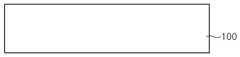
도 1은 실시예에 따른 발광소자의 단면도이다.1 is a cross-sectional view of a light emitting device according to an embodiment.
실시예에 따른 발광소자는 산화갈륨 기판(100) 상에 갈륨알루미늄을 포함하는 산화물(110), 상기 갈륨알루미늄을 포함하는 산화물(110) 상에 형성된 갈륨알루미늄을 포함하는 질화물(120) 및 상기 갈륨알루미늄을 포함하는 질화물(120) 상에 형성된 발광구조물(130)을 포함할 수 있다.The light emitting device according to the embodiment includes an
상기 갈륨알루미늄을 포함하는 산화물(110)은 GaxAlyOz(단, 0〈x≤1, 0〈y≤1,0〈z≤1)을 포함할 수 있으나 이에 한정되는 것은 아니다.The
상기 갈륨알루미늄을 포함하는 질화물(120)은 GaxAlyNz(단, 0〈x≤1, 0〈y≤1,0〈z≤1)을 포함할 수 있으나 이에 한정되는 것은 아니다.The
상기 발광구조물(130)은 상기 갈륨알루미늄을 포함하는 질화물(120) 상에 형성된 제2 도전형 반도체층(132), 상기 제2 도전형 반도체층(132) 상에 형성된 활성층(134) 및 상기 활성층(134) 상에 형성된 제1 도전형 반도체층(136)을 포함할 수 있으나 이에 한정되는 것은 아니다.The
실시예에 의하면 갈륨(Ga)과 산소(O) 사이의 결합력보다 알루미늄(Al)과 산소(O) 사이의 결합력이 더욱 강하며, 갈륨(Ga)과 질소(N) 사이의 결합력보다 알루미늄(Al)과 질소(N)의 결합력이 더욱 강하다.According to the embodiment, the bonding force between aluminum (Al) and oxygen (O) is stronger than the bonding force between gallium (Ga) and oxygen (O), and the aluminum (Al) than the bonding force between gallium (Ga) and nitrogen (N). ) And the binding force of nitrogen (N) is stronger.
이에 따라 갈륨알루미늄을 포함하는 산화물(110)과 갈륨알루미늄을 포함하는 질화물(120) 사이의 계면 결합력이 산화갈륨 기판(100)/질화물 반도체층의 발광구조물(130) 계면 결합력보다 더욱 강하여 산화갈륨 기판과 발광구조물 사이의 박리문제를 해결할 수 있다. 또한, 갈륨알루미늄을 포함하는 산화물(110)과 갈륨알루미늄을 포함하는 질화물(120) 사이의 계면 결합력이 갈륨산화질화물과 질화물 반도체층 계면의 결합력보다 강하여 박리문제를 해결할 수 있다.Accordingly, the interfacial bonding force between the
실시예에 따른 발광소자 및 그 제조방법에 의하면, 산화갈륨 기판과 계면 결합력 강화에 따른 고품위 질화물 반도체층을 구현함으로써 신뢰성이 우수하고, 성능이 우수한 발광소자 구현할 수 있다.According to the light emitting device and the manufacturing method thereof according to the embodiment, by implementing a high-quality nitride semiconductor layer by strengthening the interfacial bonding force with the gallium oxide substrate it can be implemented a light emitting device with excellent reliability and excellent performance.
이하, 도 2 내지 도 6를 참조하여 실시예에 따른 발광소자의 제조방법을 설명한다.Hereinafter, a method of manufacturing a light emitting device according to an embodiment will be described with reference to FIGS. 2 to 6.
우선, 도 2와 같이 산화갈륨 기판(100)을 준비한다. 상기 산화갈륨 기판(100)은 전도성 기판일 수 있다. 상기 산화갈륨 기판(100)은 Ga2O3기판을 포함할 수 있으나 이에 한정되는 것은 아니다.First, a
상기 산화갈륨 기판(100)은 불순물 도핑에 의해 우수한 전기 전도성을 가질 수 있다.The
상기 산화갈륨 기판(100)에 대해 습식 세척을 하여 산화갈륨 기판(100)상의 유기물 및 무기물을 제거할 수 있다.The
다음으로, 도 3과 같이 상기 산화갈륨 기판(100) 상에 갈륨알루미늄을 포함하는 산화물(110)을 형성한다. 상기 갈륨알루미늄을 포함하는 산화물(110)은 GaxAlyOz(단, 0〈x≤1, 0〈y≤1,0〈z≤1)을 포함할 수 있으나 이에 한정되는 것은 아니다.Next, as shown in FIG. 3, an
상기 갈륨알루미늄을 포함하는 산화물(110)은 원자간 결합력이 강하여 에너지 갭이 크다. 따라서 전기전도성이 산화갈륨 기판보다 작을 수 있으므로 두께를 1 ㎛ 이하로 형성할 수 있으나 이에 한정되는 것은 아니다.The
상기 갈륨알루미늄을 포함하는 산화물(110)을 형성하는 단계는 상기 산화갈륨 기판(100) 상에 박막증착장비로 증착하여 형성할 수 있다. 예를 들어, 액상에피택시, 기상에피택시, 분자선에피택시, 스퍼터링 등으로 형성할 수 있으나 이에 한정되는 것은 아니다.Forming the
또는, 상기 갈륨알루미늄을 포함하는 산화물(110)을 형성하는 단계는 상기 산화갈륨 기판(100) 상에 알루미늄층(미도시)을 형성한다. 이후, 산소분위기하에서 열처리하여 알루미늄층의 Al 원자가 상기 산화갈륨 기판(100)으로 확산하게 하여 갈륨알루미늄을 포함하는 산화물(110)을 형성할 수 있다.Alternatively, forming the
예를 들어, 상기 산화갈륨 기판(100) 상에 Al 박막층을 형성한 후, 챔버에 산소 가스 또는 산소 가스를 주된 가스로 포함하는 혼합가스를 주입하고 약 500-1200℃ 온도에서 상기 산화갈륨 기판(100)에 대한 열처리를 수행함으로써 갈륨알루 미늄을 포함하는 산화물(110)을 형성할 수 있으나 이에 한정되는 것은 아니다.For example, after forming the Al thin film layer on the
다음으로, 도 4와 같이 상기 갈륨알루미늄을 포함하는 산화물(110) 상에 갈륨알루미늄을 포함하는 질화물(120)을 형성한다.Next, as shown in FIG. 4, a
상기 갈륨알루미늄을 포함하는 질화물(120)은 GaxAlyNz(단, 0〈x≤1, 0〈y≤1,0〈z≤1)을 포함할 수 있으나 이에 한정되는 것은 아니다.The
상기 갈륨알루미늄을 포함하는 질화물(120)은 상기 갈륨알루미늄을 포함하는 산화물(110) 상에 박막증착장비로 증착할 수 있다. 예를 들어, 액상에피택시, 기상에피택시, 분자선에피택시 등으로 형성할 수 있으나 이에 한정되는 것은 아니다.The
또는, 상기 갈륨알루미늄을 포함하는 질화물(120)을 형성하는 단계는 상기 갈륨알루미늄을 포함하는 산화물(110)의 일부를 질화처리하여 형성할 수 있다.Alternatively, the forming of the
예를 들어, 상기 산화갈륨 기판(100) 상에 알루미늄층(미도시)을 형성한다. 이후, 산소분위기하에서 열처리하여 알루미늄층의 Al 원자가 상기 산화갈륨 기판(100)으로 확산하게 하여 갈륨알루미늄을 포함하는 산화물(110)을 형성한다. 이후, 상기 갈륨알루미늄을 포함하는 산화물(110)의 일부를 암모니아 분위기에서 고온의 질화처리하여 갈륨알루미늄을 포함하는 질화물(120)을 형성할 수 있다.For example, an aluminum layer (not shown) is formed on the
상기 고온 질화처리는 챔버에 암모니아 가스, 또는 암모니아 가스와 산소 가스의 혼합가스, 또는 암모니아 가스와 질소 가스의 혼합가스를 주입하여 실시할 수 있다.The high temperature nitriding treatment may be performed by injecting ammonia gas, a mixed gas of ammonia gas and oxygen gas, or a mixed gas of ammonia gas and nitrogen gas into the chamber.
이때, 상기 챔버에 주입되는 가스에 불순물 가스를 주입함으로써 상기 갈륨알루미늄을 포함하는 질화물(120)의 전기 전도성을 향상시킬 수도 있다.In this case, the electrical conductivity of the
실시예에 의하면 갈륨(Ga)과 산소(O) 사이의 결합력보다 알루미늄(Al)과 산소(O) 사이의 결합력이 더욱 강하며, 갈륨(Ga)과 질소(N) 사이의 결합력보다 알루미늄(Al)과 질소(N)의 결합력이 더욱 강하다.According to the embodiment, the bonding force between aluminum (Al) and oxygen (O) is stronger than the bonding force between gallium (Ga) and oxygen (O), and the aluminum (Al) than the bonding force between gallium (Ga) and nitrogen (N). ) And the binding force of nitrogen (N) is stronger.
이에 따라 갈륨알루미늄을 포함하는 산화물(110)과 갈륨알루미늄을 포함하는 질화물(120) 사이의 계면 결합력이 산화갈륨 기판(100)/질화물 반도체층의 발광구조물(130) 계면 결합력보다 더욱 강하여 산화갈륨 기판과 발광구조물 사이의 박리문제를 해결할 수 있다.Accordingly, the interfacial bonding force between the
실시예에 따른 발광소자 및 그 제조방법에 의하면, 산화갈륨 기판과의 계면 결합력 강화에 따른 고품위 질화물 반도체층을 구현함으로써 신뢰성이 우수하고, 성능이 우수한 발광소자 구현할 수 있다.According to the light emitting device and the manufacturing method according to the embodiment, by implementing a high-quality nitride semiconductor layer by strengthening the interfacial bonding force with the gallium oxide substrate it can be implemented a light emitting device with excellent reliability, excellent performance.
다음으로, 도 5와 같이 상기 갈륨알루미늄을 포함하는 질화물(120) 상에 발광구조물(130)을 형성할 수 있다. 도 6은 발광구조물(130)에 대한 부분 확대도이다.Next, as shown in FIG. 5, the
상기 발광구조물(130)은 상기 갈륨알루미늄을 포함하는 질화물(120) 상에 형성된 제2 도전형 반도체층(132), 상기 제2 도전형 반도체층(132) 상에 형성된 활성층(134) 및 상기 활성층(134) 상에 형성된 제1 도전형 반도체층(136)을 포함할 수 있으나 이에 한정되는 것은 아니다.The
실시예에서의 발광소자의 발광구조물(130)은 GaN, GaAs, GaAsP, GaP 등의 물질로 형성될 수 있다. 예를 들어, Green~Blue LED는 GaN(InGaN), Yellow~Red LED는 InGaAIP, AIGaAs를 사용할 수 있으며, 물질의 조성의 변경에 따라 Full Color 구현 도 가능하다.The
상기 제2 도전형 반도체층(132)은 챔버에 트리메틸 갈륨 가스(TMGa), 암모니아 가스(NH3), 질소 가스(N2), 및 마그네슘(Mg)과 같은 p 형 불순물을 포함하는 비세틸 사이클로 펜타디에닐 마그네슘(EtCp2Mg){Mg(C2H5C5H4)2}가 주입되어 p형 GaN층이 형성될 수 있으나 이에 한정되는 것은 아니다.The second conductivity-
상기 활성층(134)은 제1 도전형 반도체층(136)을 통해서 주입되는 전자와 제2 도전형 반도체층(132)을 통해서 주입되는 정공이 서로 만나서 활성층(발광층) 물질 고유의 에너지 밴드에 의해서 결정되는 에너지를 갖는 빛을 방출하는 층이다.The
상기 활성층(134)은 단일 양자 우물 구조, 다중 양자 우물 구조(MQW: Multi Quantum Well), 양자 선(Quantum-Wire) 구조, 또는 양자 점(Quantum Dot) 구조 중 적어도 어느 하나로 형성될 수 있다. 예를 들어, 상기 활성층(134)은 트리메틸 갈륨 가스(TMGa), 암모니아 가스(NH3), 질소 가스(N2), 및 트리메틸 인듐 가스(TMIn)가 주입되어 InGaN/GaN 구조를 갖는 다중 양자우물구조가 형성될 수 있으나 이에 한정되는 것은 아니다.The
상기 제1 도전형 반도체층(136)은 화학증착방법(CVD) 혹은 분자선 에피택시 (MBE) 혹은 스퍼터링 혹은 수산화물 증기상 에피택시(HVPE) 등의 방법을 사용하여 N형 GaN층을 형성할 수 있다. 또한, 상기 제1 도전형 반도체층(136)은 챔버에 트리메틸 갈륨 가스(TMGa), 암모니아 가스(NH3), 질소 가스(N2), 및 실리콘(Si)와 같은 n 형 불순물을 포함하는 실란 가스(SiH4)가 주입되어 형성될 수 있다.The first
이후, 상기 산화갈륨 기판(100)의 하측에 제2 전극(미도시)을 형성하고, 상기 제1 도전형 반도체층(136) 상에 제1 전극(미도시)을 형성할 수 있다.Thereafter, a second electrode (not shown) may be formed below the
상기 제2 전극은 오믹층(미도시), 반사층(미도시) 등을 포함할 수 있다.The second electrode may include an ohmic layer (not shown), a reflective layer (not shown), and the like.
예를 들어, 상기 제2 전극은 오믹층을 포함할 수 있으며, 정공주입을 효율적으로 할 수 있도록 단일 금속 혹은 금속합금, 금속산화물 등을 다중으로 적층하여 형성할 수 있다. 예를 들어, 상기 오믹층은 ITO, IZO(In-ZnO), GZO(Ga-ZnO), AZO(Al-ZnO), AGZO(Al-Ga ZnO), IGZO(In-Ga ZnO), IrOx, RuOx, RuOx/ITO, Ni/IrOx/Au, 및 Ni/IrOx/Au/ITO 중 적어도 하나를 포함하여 형성될 수 있으며, 이러한 재료에 한정되는 않는다.For example, the second electrode may include an ohmic layer, and may be formed by stacking a single metal, a metal alloy, a metal oxide, or the like in multiple layers so as to efficiently inject holes. For example, the ohmic layer may include ITO, IZO (In-ZnO), GZO (Ga-ZnO), AZO (Al-ZnO), AGZO (Al-Ga ZnO), IGZO (In-Ga ZnO), IrOx, RuOx. At least one of RuOx / ITO, Ni / IrOx / Au, and Ni / IrOx / Au / ITO, but is not limited thereto.
또한, 상기 제2 전극이 반사층을 포함하는 경우 Al, Ag, 혹은 Al이나 Ag를 포함하는 합금을 포함하는 금속층으로 이루어질 수 있다. 알루미늄이나 은 등은 활성층에서 발생된 빛을 효과적으로 반사하여 발광소자의 광추출 효율을 크게 개선할 수 있다.In addition, when the second electrode includes a reflective layer, the second electrode may be formed of a metal layer including Al, Ag, or an alloy including Al or Ag. Aluminum or silver can effectively reflect the light generated from the active layer to greatly improve the light extraction efficiency of the light emitting device.
실시예에 따른 발광소자 및 그 제조방법에 의하면, 산화갈륨 기판과의 계면 결합력 강화에 따른 고품위 질화물 반도체층을 구현함으로써 신뢰성이 우수하고, 성능이 우수한 발광소자 구현할 수 있다.According to the light emitting device and the manufacturing method according to the embodiment, by implementing a high-quality nitride semiconductor layer by strengthening the interfacial bonding force with the gallium oxide substrate it can be implemented a light emitting device with excellent reliability, excellent performance.
이상에서 실시예를 중심으로 설명하였으나 이는 단지 예시일 뿐 본 발명을 한정하는 것이 아니며, 본 발명이 속하는 분야의 통상의 지식을 가진 자라면 본 실시예의 본질적인 특성을 벗어나지 않는 범위에서 이상에 예시되지 않은 여러 가지의 변형과 응용이 가능함을 알 수 있을 것이다. 예를 들어, 실시예에 구체적으로 나타난 각 구성 요소는 변형하여 실시할 수 있는 것이다. 그리고 이러한 변형과 응용에 관계된 차이점들은 첨부된 청구 범위에서 규정하는 본 발명의 범위에 포함되는 것으로 해석되어야 할 것이다.Although the above description has been made based on the embodiments, these are merely examples and are not intended to limit the present invention. Those skilled in the art to which the present invention pertains may not have been exemplified above without departing from the essential characteristics of the present embodiments. It will be appreciated that many variations and applications are possible. For example, each component specifically shown in the embodiment can be modified. And differences relating to such modifications and applications will have to be construed as being included in the scope of the invention defined in the appended claims.
도 1은 실시예에 따른 발광소자의 단면도.1 is a cross-sectional view of a light emitting device according to an embodiment.
도 2 내지 도 6은 실시예에 따른 발광소자의 제조방법의 공정단면도.2 to 6 are process cross-sectional views of a method of manufacturing a light emitting device according to the embodiment.
Claims (14)
Translated fromKoreanPriority Applications (7)
| Application Number | Priority Date | Filing Date | Title |
|---|---|---|---|
| KR1020090127189AKR101047652B1 (en) | 2009-12-18 | 2009-12-18 | Light emitting device and manufacturing method |
| US12/940,718US8115230B2 (en) | 2009-12-18 | 2010-11-05 | Light emitting device, light emitting device package and lighting system |
| EP10191489AEP2337093B1 (en) | 2009-12-18 | 2010-11-17 | Light emitting device, light emitting device package and lighting system |
| CN201010579308.8ACN102104093B (en) | 2009-12-18 | 2010-12-03 | Light emitting device, light emitting device package and lighting system |
| JP2010277127AJP5751696B2 (en) | 2009-12-18 | 2010-12-13 | Light emitting device, light emitting device package, and lighting system |
| US13/349,387US8349743B2 (en) | 2009-12-18 | 2012-01-12 | Method for fabricating light emitting device |
| US13/735,607US9099611B2 (en) | 2009-12-18 | 2013-01-07 | Light emitting device |
Applications Claiming Priority (1)
| Application Number | Priority Date | Filing Date | Title |
|---|---|---|---|
| KR1020090127189AKR101047652B1 (en) | 2009-12-18 | 2009-12-18 | Light emitting device and manufacturing method |
Publications (2)
| Publication Number | Publication Date |
|---|---|
| KR20110070382A KR20110070382A (en) | 2011-06-24 |
| KR101047652B1true KR101047652B1 (en) | 2011-07-07 |
Family
ID=43589886
Family Applications (1)
| Application Number | Title | Priority Date | Filing Date |
|---|---|---|---|
| KR1020090127189AExpired - Fee RelatedKR101047652B1 (en) | 2009-12-18 | 2009-12-18 | Light emitting device and manufacturing method |
Country Status (5)
| Country | Link |
|---|---|
| US (3) | US8115230B2 (en) |
| EP (1) | EP2337093B1 (en) |
| JP (1) | JP5751696B2 (en) |
| KR (1) | KR101047652B1 (en) |
| CN (1) | CN102104093B (en) |
Families Citing this family (9)
| Publication number | Priority date | Publication date | Assignee | Title |
|---|---|---|---|---|
| WO2013035472A1 (en)* | 2011-09-08 | 2013-03-14 | 株式会社タムラ製作所 | Substrate for epitaxial growth, and crystal laminate structure |
| JP5343224B1 (en)* | 2012-09-28 | 2013-11-13 | Roca株式会社 | Semiconductor device and crystal |
| JP2016015375A (en)* | 2014-07-01 | 2016-01-28 | 株式会社タムラ製作所 | Light emitting element |
| CA2964920C (en)* | 2014-10-27 | 2023-02-21 | Dow Global Technologies Llc | Plasticizer compositions and methods for making plasticizer compositions |
| JP6776931B2 (en)* | 2016-03-23 | 2020-10-28 | 三菱マテリアル株式会社 | Manufacturing method of laminated reflective electrode film, laminated reflective electrode pattern, laminated reflective electrode pattern |
| TWI577842B (en)* | 2016-05-30 | 2017-04-11 | 光鋐科技股份有限公司 | Method for growing aluminum gallium nitride |
| CN107358780B (en)* | 2017-07-30 | 2020-01-03 | 王旭兰 | Intelligent electric spark detection alarm system based on PN junction chip and preparation method thereof |
| US20210013374A1 (en)* | 2018-03-19 | 2021-01-14 | King Abdullah University Of Science And Technology | Iii-nitride optoelectronic devices and method of production |
| WO2024228767A1 (en)* | 2023-05-04 | 2024-11-07 | Ohio State Innovation Foundation | Devices comprising a thick (alzga1-z)2o3 layer on a (001) ga2o3 substrate using a (alxga1-x)2o3 buffer layer, and methods of making and use thereof |
Citations (2)
| Publication number | Priority date | Publication date | Assignee | Title |
|---|---|---|---|---|
| JP2005072094A (en)* | 2003-08-20 | 2005-03-17 | ▲さん▼圓光電股▲ふん▼有限公司 | Light emitting diode device where selective growth is applied |
| KR20080049869A (en)* | 2006-12-01 | 2008-06-05 | 서울옵토디바이스주식회사 | Nitride Semiconductor Light Emitting Diode and Manufacturing Method Thereof |
Family Cites Families (26)
| Publication number | Priority date | Publication date | Assignee | Title |
|---|---|---|---|---|
| JP3679097B2 (en)* | 2002-05-31 | 2005-08-03 | 株式会社光波 | Light emitting element |
| TWI303909B (en)* | 2002-11-25 | 2008-12-01 | Nichia Corp | Ridge waveguide semiconductor laser diode |
| JP4754164B2 (en) | 2003-08-08 | 2011-08-24 | 株式会社光波 | Semiconductor layer |
| TW200520266A (en)* | 2003-11-21 | 2005-06-16 | Sanken Electric Co Ltd | Semiconductor luminous element and manufacturing method of the same |
| JP4670034B2 (en)* | 2004-03-12 | 2011-04-13 | 学校法人早稲田大学 | Ga2O3-based semiconductor layer provided with electrodes |
| WO2005122349A1 (en)* | 2004-06-07 | 2005-12-22 | Nl Nanosemiconductor Gmbh | Electrooptically wavelength-tunable resonant cavity optoelectronic device for high-speed data transfer |
| JP4624131B2 (en)* | 2005-02-22 | 2011-02-02 | 三洋電機株式会社 | Nitride semiconductor device manufacturing method |
| KR100593937B1 (en)* | 2005-03-30 | 2006-06-30 | 삼성전기주식회사 | LED package using Si substrate and manufacturing method thereof |
| JP5159040B2 (en)* | 2005-03-31 | 2013-03-06 | 株式会社光波 | Method for forming low temperature growth buffer layer and method for manufacturing light emitting device |
| KR100691159B1 (en)* | 2005-04-30 | 2007-03-09 | 삼성전기주식회사 | Method of manufacturing gallium nitride based semiconductor |
| US8008215B2 (en)* | 2005-05-12 | 2011-08-30 | Massachusetts Institute Of Technology | Integration of buried oxide layers with crystalline layers |
| JP4225510B2 (en)* | 2005-07-06 | 2009-02-18 | 昭和電工株式会社 | Compound semiconductor light emitting diode and method for manufacturing the same |
| JP3998027B2 (en)* | 2005-07-25 | 2007-10-24 | 松下電工株式会社 | Lighting equipment using LED |
| JP5180430B2 (en)* | 2005-08-04 | 2013-04-10 | 独立行政法人物質・材料研究機構 | Light emitting element |
| JP2007234902A (en)* | 2006-03-01 | 2007-09-13 | Toyoda Gosei Co Ltd | LIGHT EMITTING ELEMENT AND MANUFACTURING METHOD THEREOF |
| US20070134833A1 (en)* | 2005-12-14 | 2007-06-14 | Toyoda Gosei Co., Ltd. | Semiconductor element and method of making same |
| JP2007165626A (en)* | 2005-12-14 | 2007-06-28 | Toyoda Gosei Co Ltd | Light emitting device and manufacturing method thereof |
| CN101852349B (en)* | 2005-12-22 | 2012-08-29 | 松下电器产业株式会社 | Lighting apparatus with led |
| KR100795547B1 (en) | 2006-06-30 | 2008-01-21 | 서울옵토디바이스주식회사 | Nitride semiconductor light emitting device |
| KR100915502B1 (en) | 2007-01-18 | 2009-09-03 | 광주과학기술원 | Light-Emitting Diode using Surface Plasmon |
| JP2008258042A (en)* | 2007-04-06 | 2008-10-23 | Hitachi Displays Ltd | LIGHTING DEVICE AND DISPLAY DEVICE USING THE LIGHTING DEVICE |
| JP2009060005A (en)* | 2007-09-03 | 2009-03-19 | Nippon Light Metal Co Ltd | LIGHT EMITTING ELEMENT AND MANUFACTURING METHOD THEREOF |
| TWI362765B (en)* | 2007-09-07 | 2012-04-21 | Epistar Corp | Light emitting diode device and manufacturing method therof |
| JP2009091217A (en) | 2007-10-11 | 2009-04-30 | Nippon Light Metal Co Ltd | Gallium-aluminum oxide crystal film, method for producing the same, and semiconductor device using the same |
| KR100998007B1 (en) | 2007-11-23 | 2010-12-03 | 삼성엘이디 주식회사 | Nitride semiconductor light emitting device |
| WO2011155302A1 (en)* | 2010-06-11 | 2011-12-15 | Semiconductor Energy Laboratory Co., Ltd. | Semiconductor device |
- 2009
- 2009-12-18KRKR1020090127189Apatent/KR101047652B1/ennot_activeExpired - Fee Related
- 2010
- 2010-11-05USUS12/940,718patent/US8115230B2/enactiveActive
- 2010-11-17EPEP10191489Apatent/EP2337093B1/enactiveActive
- 2010-12-03CNCN201010579308.8Apatent/CN102104093B/enactiveActive
- 2010-12-13JPJP2010277127Apatent/JP5751696B2/enactiveActive
- 2012
- 2012-01-12USUS13/349,387patent/US8349743B2/enactiveActive
- 2013
- 2013-01-07USUS13/735,607patent/US9099611B2/enactiveActive
Patent Citations (2)
| Publication number | Priority date | Publication date | Assignee | Title |
|---|---|---|---|---|
| JP2005072094A (en)* | 2003-08-20 | 2005-03-17 | ▲さん▼圓光電股▲ふん▼有限公司 | Light emitting diode device where selective growth is applied |
| KR20080049869A (en)* | 2006-12-01 | 2008-06-05 | 서울옵토디바이스주식회사 | Nitride Semiconductor Light Emitting Diode and Manufacturing Method Thereof |
Also Published As
| Publication number | Publication date |
|---|---|
| US20120115267A1 (en) | 2012-05-10 |
| EP2337093A1 (en) | 2011-06-22 |
| US20130119402A1 (en) | 2013-05-16 |
| CN102104093A (en) | 2011-06-22 |
| US20110147771A1 (en) | 2011-06-23 |
| KR20110070382A (en) | 2011-06-24 |
| EP2337093B1 (en) | 2013-01-02 |
| US8349743B2 (en) | 2013-01-08 |
| US9099611B2 (en) | 2015-08-04 |
| JP2011129915A (en) | 2011-06-30 |
| JP5751696B2 (en) | 2015-07-22 |
| US8115230B2 (en) | 2012-02-14 |
| CN102104093B (en) | 2015-06-17 |
Similar Documents
| Publication | Publication Date | Title |
|---|---|---|
| KR101047652B1 (en) | Light emitting device and manufacturing method | |
| KR101134731B1 (en) | Light emitting device and method for fabricating the same | |
| KR101646255B1 (en) | Light emitting device, light emitting device package and method for fabricating the light emitting device | |
| KR101039988B1 (en) | Light emitting device and method of manufacturing | |
| KR101294518B1 (en) | Nitride semiconductor light-emitting device and manufacturing method thereof | |
| KR20110062128A (en) | Light emitting device, light emitting device package and manufacturing method | |
| CN101834242B (en) | Light emitting device | |
| KR20110027296A (en) | Light emitting device and manufacturing method | |
| KR101114047B1 (en) | Light emitting device and method for fabricating the same | |
| KR101072200B1 (en) | Light emitting device and method for fabricating the same | |
| TWI513062B (en) | Light-emitting element package structure and method of manufacturing same | |
| KR102249624B1 (en) | Light emitting structure and Light emitting device having the same | |
| JP6948494B2 (en) | UV light emitting element and light emitting element package | |
| KR101198759B1 (en) | Nitride light emitting device | |
| KR100999695B1 (en) | Semiconductor light emitting device and manufacturing method thereof | |
| KR102249630B1 (en) | Light emitting device and lighting system | |
| KR100986327B1 (en) | Light emitting device and method for fabricating the same | |
| US8319227B2 (en) | Light emitting device | |
| KR101232069B1 (en) | Light emitting device and method fabricating the same | |
| KR101755670B1 (en) | Light emitting device and method for fabricating light emitting device | |
| KR20130006978A (en) | Light emitting device and method for fabricating the same | |
| CN106601878A (en) | Preparation method for LED with high light efficiency | |
| KR102462717B1 (en) | Light Emitting Device | |
| TW202406170A (en) | Light-emitting device and manufacturing method thereof | |
| KR101199796B1 (en) | Nitride semiconductor light emitting device and method for manufacturing thereof |
Legal Events
| Date | Code | Title | Description |
|---|---|---|---|
| A201 | Request for examination | ||
| PA0109 | Patent application | St.27 status event code:A-0-1-A10-A12-nap-PA0109 | |
| PA0201 | Request for examination | St.27 status event code:A-1-2-D10-D11-exm-PA0201 | |
| R18-X000 | Changes to party contact information recorded | St.27 status event code:A-3-3-R10-R18-oth-X000 | |
| A302 | Request for accelerated examination | ||
| PA0302 | Request for accelerated examination | St.27 status event code:A-1-2-D10-D17-exm-PA0302 St.27 status event code:A-1-2-D10-D16-exm-PA0302 | |
| D13-X000 | Search requested | St.27 status event code:A-1-2-D10-D13-srh-X000 | |
| D14-X000 | Search report completed | St.27 status event code:A-1-2-D10-D14-srh-X000 | |
| E902 | Notification of reason for refusal | ||
| PE0902 | Notice of grounds for rejection | St.27 status event code:A-1-2-D10-D21-exm-PE0902 | |
| P11-X000 | Amendment of application requested | St.27 status event code:A-2-2-P10-P11-nap-X000 | |
| P13-X000 | Application amended | St.27 status event code:A-2-2-P10-P13-nap-X000 | |
| E701 | Decision to grant or registration of patent right | ||
| PE0701 | Decision of registration | St.27 status event code:A-1-2-D10-D22-exm-PE0701 | |
| PG1501 | Laying open of application | St.27 status event code:A-1-1-Q10-Q12-nap-PG1501 | |
| GRNT | Written decision to grant | ||
| PR0701 | Registration of establishment | St.27 status event code:A-2-4-F10-F11-exm-PR0701 | |
| PR1002 | Payment of registration fee | St.27 status event code:A-2-2-U10-U11-oth-PR1002 Fee payment year number:1 | |
| PG1601 | Publication of registration | St.27 status event code:A-4-4-Q10-Q13-nap-PG1601 | |
| FPAY | Annual fee payment | Payment date:20140609 Year of fee payment:4 | |
| PR1001 | Payment of annual fee | St.27 status event code:A-4-4-U10-U11-oth-PR1001 Fee payment year number:4 | |
| PN2301 | Change of applicant | St.27 status event code:A-5-5-R10-R13-asn-PN2301 St.27 status event code:A-5-5-R10-R11-asn-PN2301 | |
| FPAY | Annual fee payment | Payment date:20150605 Year of fee payment:5 | |
| PR1001 | Payment of annual fee | St.27 status event code:A-4-4-U10-U11-oth-PR1001 Fee payment year number:5 | |
| FPAY | Annual fee payment | Payment date:20160607 Year of fee payment:6 | |
| PR1001 | Payment of annual fee | St.27 status event code:A-4-4-U10-U11-oth-PR1001 Fee payment year number:6 | |
| R18-X000 | Changes to party contact information recorded | St.27 status event code:A-5-5-R10-R18-oth-X000 | |
| FPAY | Annual fee payment | Payment date:20170605 Year of fee payment:7 | |
| PR1001 | Payment of annual fee | St.27 status event code:A-4-4-U10-U11-oth-PR1001 Fee payment year number:7 | |
| LAPS | Lapse due to unpaid annual fee | ||
| PC1903 | Unpaid annual fee | St.27 status event code:A-4-4-U10-U13-oth-PC1903 Not in force date:20180702 Payment event data comment text:Termination Category : DEFAULT_OF_REGISTRATION_FEE | |
| R18-X000 | Changes to party contact information recorded | St.27 status event code:A-5-5-R10-R18-oth-X000 | |
| PC1903 | Unpaid annual fee | St.27 status event code:N-4-6-H10-H13-oth-PC1903 Ip right cessation event data comment text:Termination Category : DEFAULT_OF_REGISTRATION_FEE Not in force date:20180702 | |
| R18-X000 | Changes to party contact information recorded | St.27 status event code:A-5-5-R10-R18-oth-X000 | |
| PN2301 | Change of applicant | St.27 status event code:A-5-5-R10-R13-asn-PN2301 St.27 status event code:A-5-5-R10-R11-asn-PN2301 |