KR101047601B1 - Backlight unit and display device using same - Google Patents
Backlight unit and display device using sameDownload PDFInfo
- Publication number
- KR101047601B1 KR101047601B1KR1020090079030AKR20090079030AKR101047601B1KR 101047601 B1KR101047601 B1KR 101047601B1KR 1020090079030 AKR1020090079030 AKR 1020090079030AKR 20090079030 AKR20090079030 AKR 20090079030AKR 101047601 B1KR101047601 B1KR 101047601B1
- Authority
- KR
- South Korea
- Prior art keywords
- guide plate
- light guide
- backlight unit
- light
- optical assemblies
- Prior art date
- Legal status (The legal status is an assumption and is not a legal conclusion. Google has not performed a legal analysis and makes no representation as to the accuracy of the status listed.)
- Expired - Fee Related
Links
Images


Classifications
- G—PHYSICS
- G02—OPTICS
- G02B—OPTICAL ELEMENTS, SYSTEMS OR APPARATUS
- G02B6/00—Light guides; Structural details of arrangements comprising light guides and other optical elements, e.g. couplings
- G02B6/0001—Light guides; Structural details of arrangements comprising light guides and other optical elements, e.g. couplings specially adapted for lighting devices or systems
- G02B6/0011—Light guides; Structural details of arrangements comprising light guides and other optical elements, e.g. couplings specially adapted for lighting devices or systems the light guides being planar or of plate-like form
- G02B6/0075—Arrangements of multiple light guides
- G02B6/0078—Side-by-side arrangements, e.g. for large area displays
- G02B6/008—Side-by-side arrangements, e.g. for large area displays of the partially overlapping type
- G—PHYSICS
- G02—OPTICS
- G02F—OPTICAL DEVICES OR ARRANGEMENTS FOR THE CONTROL OF LIGHT BY MODIFICATION OF THE OPTICAL PROPERTIES OF THE MEDIA OF THE ELEMENTS INVOLVED THEREIN; NON-LINEAR OPTICS; FREQUENCY-CHANGING OF LIGHT; OPTICAL LOGIC ELEMENTS; OPTICAL ANALOGUE/DIGITAL CONVERTERS
- G02F1/00—Devices or arrangements for the control of the intensity, colour, phase, polarisation or direction of light arriving from an independent light source, e.g. switching, gating or modulating; Non-linear optics
- G02F1/01—Devices or arrangements for the control of the intensity, colour, phase, polarisation or direction of light arriving from an independent light source, e.g. switching, gating or modulating; Non-linear optics for the control of the intensity, phase, polarisation or colour
- G02F1/13—Devices or arrangements for the control of the intensity, colour, phase, polarisation or direction of light arriving from an independent light source, e.g. switching, gating or modulating; Non-linear optics for the control of the intensity, phase, polarisation or colour based on liquid crystals, e.g. single liquid crystal display cells
- G02F1/133—Constructional arrangements; Operation of liquid crystal cells; Circuit arrangements
- G02F1/1333—Constructional arrangements; Manufacturing methods
- G02F1/1335—Structural association of cells with optical devices, e.g. polarisers or reflectors
- G—PHYSICS
- G02—OPTICS
- G02B—OPTICAL ELEMENTS, SYSTEMS OR APPARATUS
- G02B6/00—Light guides; Structural details of arrangements comprising light guides and other optical elements, e.g. couplings
- G02B6/0001—Light guides; Structural details of arrangements comprising light guides and other optical elements, e.g. couplings specially adapted for lighting devices or systems
- G02B6/0011—Light guides; Structural details of arrangements comprising light guides and other optical elements, e.g. couplings specially adapted for lighting devices or systems the light guides being planar or of plate-like form
- G02B6/0033—Means for improving the coupling-out of light from the light guide
- G02B6/005—Means for improving the coupling-out of light from the light guide provided by one optical element, or plurality thereof, placed on the light output side of the light guide
- G02B6/0051—Diffusing sheet or layer
- G—PHYSICS
- G02—OPTICS
- G02B—OPTICAL ELEMENTS, SYSTEMS OR APPARATUS
- G02B6/00—Light guides; Structural details of arrangements comprising light guides and other optical elements, e.g. couplings
- G02B6/0001—Light guides; Structural details of arrangements comprising light guides and other optical elements, e.g. couplings specially adapted for lighting devices or systems
- G02B6/0011—Light guides; Structural details of arrangements comprising light guides and other optical elements, e.g. couplings specially adapted for lighting devices or systems the light guides being planar or of plate-like form
- G02B6/0033—Means for improving the coupling-out of light from the light guide
- G02B6/005—Means for improving the coupling-out of light from the light guide provided by one optical element, or plurality thereof, placed on the light output side of the light guide
- G02B6/0053—Prismatic sheet or layer; Brightness enhancement element, sheet or layer
- G—PHYSICS
- G02—OPTICS
- G02B—OPTICAL ELEMENTS, SYSTEMS OR APPARATUS
- G02B6/00—Light guides; Structural details of arrangements comprising light guides and other optical elements, e.g. couplings
- G02B6/0001—Light guides; Structural details of arrangements comprising light guides and other optical elements, e.g. couplings specially adapted for lighting devices or systems
- G02B6/0011—Light guides; Structural details of arrangements comprising light guides and other optical elements, e.g. couplings specially adapted for lighting devices or systems the light guides being planar or of plate-like form
- G02B6/0033—Means for improving the coupling-out of light from the light guide
- G02B6/005—Means for improving the coupling-out of light from the light guide provided by one optical element, or plurality thereof, placed on the light output side of the light guide
- G02B6/0055—Reflecting element, sheet or layer
- G—PHYSICS
- G02—OPTICS
- G02B—OPTICAL ELEMENTS, SYSTEMS OR APPARATUS
- G02B6/00—Light guides; Structural details of arrangements comprising light guides and other optical elements, e.g. couplings
- G02B6/0001—Light guides; Structural details of arrangements comprising light guides and other optical elements, e.g. couplings specially adapted for lighting devices or systems
- G02B6/0011—Light guides; Structural details of arrangements comprising light guides and other optical elements, e.g. couplings specially adapted for lighting devices or systems the light guides being planar or of plate-like form
- G02B6/0066—Light guides; Structural details of arrangements comprising light guides and other optical elements, e.g. couplings specially adapted for lighting devices or systems the light guides being planar or of plate-like form characterised by the light source being coupled to the light guide
- G02B6/0068—Arrangements of plural sources, e.g. multi-colour light sources
Landscapes
- Physics & Mathematics (AREA)
- General Physics & Mathematics (AREA)
- Optics & Photonics (AREA)
- Nonlinear Science (AREA)
- Mathematical Physics (AREA)
- Chemical & Material Sciences (AREA)
- Crystallography & Structural Chemistry (AREA)
- Planar Illumination Modules (AREA)
Abstract
Translated fromKoreanDescription
Translated fromKorean실시예는 백라이트 유닛 및 이를 이용한 디스플레이 장치에 관한 것이다.An embodiment relates to a backlight unit and a display device using the same.
근래에 각광받고 있는 액정표시장치(LCD : liquid crystal display device)는 소형화, 경량화 및 저전력 소비화 등의 이점을 가지고 있어서 기존의 브라운관(CRT : cathode ray tube)의 단점을 극복할 수 있는 대체 수단으로서 점차 주목받아 왔고, 현재는 디스플레이 장치가 필요한 거의 모든 정보처리 기기에 장착되어 사용되고 있다.Liquid crystal display devices (LCDs), which have been in the spotlight recently, have advantages such as miniaturization, light weight, and low power consumption, and as an alternative means to overcome the disadvantages of the conventional cathode ray tube (CRT). It has been attracting attention gradually and is currently used in almost all information processing devices that require a display device.
이와 같은 액정표시장치는 자발광 표시장치가 아니기 때문에 백라이트 유닛(Back Light Unit : BLU)과 같은 별도의 광원이 필요하다. 상기 백라이트 유닛에서 발광되는 광을 효과적으로 활용하여 고 품질의 영상을 제공하기 위해 많은 연구가 진행되고 있다.Since the liquid crystal display is not a self-luminous display, a separate light source such as a back light unit (BLU) is required. In order to effectively utilize the light emitted from the backlight unit, many studies have been conducted to provide a high quality image.
실시예는 새로운 구조의 백라이트 유닛 및 이를 이용한 디스플레이 장치를 제공한다.The embodiment provides a backlight unit having a new structure and a display device using the same.
실시예는 다수의 광학 어셈블리를 포함하는 백라이트 유닛을 제공한다.Embodiments provide a backlight unit comprising a plurality of optical assemblies.
실시예는 간단한 구조를 가지는 광학 어셈블리를 포함하는 백라이트 유닛을 제공한다.The embodiment provides a backlight unit including an optical assembly having a simple structure.
실시예에 따른 백라이트 유닛은 도광판; 및 상기 도광판의 일 측을 향해 광을 입사하는 발광모듈부를 포함하는 다수의 광학 어셈블리를 포함하며, 상기 다수의 광학 어셈블리들은 각각 제1 각도로 기울어져 적어도 일부가 중첩되도록 배치된다.The backlight unit according to the embodiment includes a light guide plate; And a plurality of optical assemblies including a light emitting module unit for injecting light toward one side of the light guide plate, wherein the plurality of optical assemblies are inclined at a first angle and at least partially overlap each other.
실시예에 따른 디스플레이 장치는 도광판과, 상기 도광판의 일 측에 배치되어 상기 도광판의 일 측을 향해 광을 입사하는 발광모듈부를 포함하는 다수의 광학 어셈블리를 포함하며, 상기 다수의 광학 어셈블리는 적어도 일부가 중첩되도록 배치된 백라이트 유닛; 상기 백라이트 유닛 상에 배치되어, 상기 백라이트 유닛으로부터 광을 제공받아 영상을 디스플레이 하는 표시 패널; 및 상기 백라이트 유닛을 수용하고 지지하는 바텀 커버를 포함하며, 상기 다수의 광학 어셈블리들은 상기 표시 패널과 제1 각도를 가지도록 기울어져 배치된다.The display apparatus according to the embodiment includes a plurality of optical assemblies including a light guide plate and a light emitting module unit disposed on one side of the light guide plate to inject light toward one side of the light guide plate, wherein the plurality of optical assemblies are at least partially. A backlight unit disposed to overlap with each other; A display panel disposed on the backlight unit to receive light from the backlight unit to display an image; And a bottom cover configured to receive and support the backlight unit, wherein the plurality of optical assemblies are inclined to have a first angle with the display panel.
실시예는 새로운 구조의 백라이트 유닛 및 이를 이용한 디스플레이 장치를 제공할 수 있다.The embodiment can provide a backlight unit having a new structure and a display device using the same.
실시예는 다수의 광학 어셈블리를 포함하는 백라이트 유닛을 제공할 수 있다.Embodiments may provide a backlight unit including a plurality of optical assemblies.
실시예는 간단한 구조를 가지는 광학 어셈블리를 포함하는 백라이트 유닛을 제공할 수 있다.The embodiment can provide a backlight unit including an optical assembly having a simple structure.
실시예는 제조 공정이 간단한 백라이트 유닛을 제공할 수 있다.The embodiment can provide a backlight unit having a simple manufacturing process.
실시예는 교체가 용이한 백라이트 유닛을 제공할 수 있다.The embodiment may provide a backlight unit that is easy to replace.
실시예는 대형 표시 패널에 적용이 유리한 백라이트 유닛을 제공할 수 있다.The embodiment can provide a backlight unit that can be advantageously applied to a large display panel.
실시예는 슬림한 두께를 가지는 백라이트 유닛을 제공할 수 있다.The embodiment can provide a backlight unit having a slim thickness.
실시예의 설명에 있어서, 각 층(막), 영역, 패턴 또는 구조물들이 기판, 각 층(막), 영역, 패드 또는 패턴들의 "상/위(on)"에 또는 "아래(under)"에 형성되는 것으로 기재되는 경우에 있어, "상/위(on)"와 "아래(under)"는 "직접(directly)" 또는 "다른 층을 개재하여 (indirectly)" 형성되는 것을 모두 포함한다. 또한 각 층의 상/위 또는 아래에 대한 기준은 도면을 기준으로 설명한다.In the description of an embodiment, each layer (film), region, pattern, or structure is formed “on” or “under” a substrate, each layer (film), region, pad, or pattern. In the case where it is described as "to", "on" and "under" include both "directly" or "indirectly" formed. Also, the criteria for top, bottom, or bottom of each layer will be described with reference to the drawings.
도면에서 각층의 두께나 크기는 설명의 편의 및 명확성을 위하여 과장되거나 생략되거나 또는 개략적으로 도시되었다. 또한 각 구성요소의 크기는 실제크기를 전적으로 반영하는 것은 아니다.In the drawings, the thickness or size of each layer is exaggerated, omitted, or schematically illustrated for convenience and clarity of description. In addition, the size of each component does not necessarily reflect the actual size.
이하, 도면을 참조하여 실시예에 따른 백라이트 유닛 및 이를 이용한 디스플 레이 장치에 대해 설명한다.Hereinafter, a backlight unit and a display device using the same will be described with reference to the accompanying drawings.
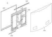
도 1은 실시예에 따른 디스플레이 장치(1)의 분해 사시도이다.1 is an exploded perspective view of a display device 1 according to an embodiment.
도 1을 참조하면, 실시예에 따른 디스플레이 장치(1)는 디스플레이 모듈(200)과, 디스플레이 모듈(200)을 둘러싸는 프론트 커버(300) 및 백 커버(400)와, 디스플레이 모듈(200)을 프론트 커버(300) 및/또는 백 커버(400)에 고정시키기 위한 고정부재(500)를 포함한다.Referring to FIG. 1, the display apparatus 1 according to the embodiment includes a
상기 고정 부재(500)는 상기 프론트 커버(300)와 상기 디스플레이 모듈(200) 사이에 배치될 수 있다. 상기 고정 부재(500)의 일측은 상기 프론트 커버(300)에 예를 들어, 스크류와 같은 체결부재에 의하여 고정되고, 타측은 상기 디스플레이 모듈(200)을 상기 프론트 커버(300)에 고정하여, 상기 프론트 커버(300)에 대하여 상기 디스플레이 모듈(200)이 고정되도록 할 수 있다.The
실시예에서는 상기 고정부재(500)가 일례로 일 방향으로 길게 연장된 플레이트 형상으로 형성되는 것으로 설명되고 있으나, 별도의 고정부재가 제공되지 아니하고, 체결부재에 의하여 상기 디스플레이 모듈(200)이 상기 프론트 커버(300) 또는 상기 백 커버(400)에 고정되는 구성 또한 가능하다고 할 것이다.In the embodiment, the
도 2는 도 1의 A-A선도에 따른 상기 디스플레이 모듈(200)의 단면도이다.2 is a cross-sectional view of the
도 2를 참조하면, 상기 디스플레이 모듈(200)은 영상이 디스플레이되는 표시 패널(210)과, 상기 표시 패널(210)에 광을 제공하는 백 라이트 유닛(100)과, 상기 디스플레이 모듈(200)의 하측 외관을 형성하는 바텀 커버(110)와, 상기 표시 패 널(210)을 하측에서 지지하는 패널 서포터(240)와, 상기 표시 패널(210)을 상측에서 지지하며, 디스플레이 모듈(200)의 테두리를 형성하는 탑 커버(230)를 포함한다.Referring to FIG. 2, the
상기 바텀 커버(110)은 상기 백 라이트 유닛(100)이 수납될 수 있도록 상면이 개구된 박스 형상으로 형성될 수 있다. 상기 바텀 커버(110)의 바닥면은 상기 백라이트 유닛(100)의 형상에 대응되도록 상기 백라이트 유닛(100)의 배면 형태를 따라 요철 구조로 형성될 수 있다.The
다만, 상기 바텀 커버(110)의 형태에 대해 한정하지는 않으며, 예를 들어, 상기 바텀 커버(110)의 바닥면은 편평하게 형성되고 상기 백라이트 유닛(100)을 지지하기 위한 지지부를 포함할 수도 있다.However, the shape of the
그리고, 상기 바텀 커버(110)의 일측은 상기 탑 커버(230)의 일측과 고정될 수 있다. 예를 들어, 상기 디스플레이 모듈(200)의 측면, 즉 상기 바텀 커버(110)와 상기 탑 커버(230)가 중첩되는 측에, 스크류와 같은 체결 부재가 관통되어, 상기 바텀 커버(110)와 상기 탑 커버(230)를 고정시킬 수 있다. 다만, 이에 대해 한정하지는 않는다.One side of the
상기 표시 패널(210)은 상세히 도시되지는 않았지만, 서로 대향하여 균일한 셀 갭(Gap)이 유지되도록 합착된 하부 기판(211) 및 상부 기판(222)과, 상기 두 기판 사이에 개재된 액정층을 포함할 수 있다. 상기 하부 기판(211)에는 다수의 게이트 라인과 상기 다수의 게이트 라인과 교차하는 다수의 데이터 라인이 형성되며, 상기 게이트 라인과 데이터 라인의 교차영역에 박막 트랜지스터(TFT: thin film transistor)가 형성될 수 있다. 상기 상부 기판(212)에는 컬러필터들이 형성될 수 있다. 다만, 상기 표시 패널(210)의 구조는 이에 한정되지는 않으며, 상기 표시 패널(210)은 다양한 구조를 가질 수 있다. 예를 들어, 상기 하부 기판(211)은 박막 트랜지스터 뿐만 아니라 컬러필터를 포함할 수도 있다. 또한, 상기 표시 패널(210)은 상기 액정층을 구동하는 방식에 따라 다양한 형태의 구조로 형성될 수 있다.Although not shown in detail, the
도시하지 않았으나, 상기 표시 패널(210)의 가장자리에는 게이트 라인에 스캔신호를 공급하는 게이트 구동 PCB(gate driving printed circuit board)와, 데이터 라인에 데이터 신호를 공급하는 데이터 구동 PCB(data driving printed circuit board)가 구비될 수 있다.Although not shown, a gate driving printed circuit board (PCB) for supplying a scan signal to a gate line and a data driving printed circuit board (PCB) for supplying a data signal to a data line are provided at edges of the display panel 210. ) May be provided.
상기 표시 패널(210)의 위 및 아래 중 적어도 한 곳에는 편광 필름(미도시)이 배치될 수도 있다.A polarizing film (not shown) may be disposed on at least one of the top and bottom of the
상기 표시 패널(210)과 백라이트 유닛(100) 사이에는 광학 시트(220)가 배치될 수 있으며, 이에 대해 한정하지는 않는다.An
상기 광학 시트(220)는 확산 시트 또는/및 프리즘 시트를 포함할 수 있다.The
상기 확산 시트는 상기 도광판에서 출사된 광을 고르게 확산시켜 주며, 상기 확산된 광은 프리즘 시트에 의해 표시 패널로 집광될 수 있다. 여기서, 상기 프리즘 시트는 수평 또는/및 수직 프리즘 시트, 한 장 이상의 조도 강화 필름 등을 이용하여 선택적으로 구성할 수 있다. 상기 광학 시트(220)의 종류나 개수 등은 실시 예의 기술적 범위 내에서 추가 또는 삭제될 수 있으며, 이에 대해 한정하지는 않는다.The diffusion sheet evenly spreads the light emitted from the light guide plate, and the diffused light may be focused onto the display panel by the prism sheet. Here, the prism sheet may be selectively configured using a horizontal or / and vertical prism sheet, one or more roughness reinforcing films, and the like. Type or number of the
한편, 상기 백라이트 유닛(100)은 다수의 분할 구동 영역을 형성하는 다수의 광학 어셈블리(10)를 포함한다. 그리고, 각각의 상기 광학 어셈블리(10)들에 대응하여 상기 표시 패널(210)은 다수의 분할 영역을 가지며, 상기 분할 영역의 그레이 피크값 또는 색 좌표 신호에 따라 상기 광학 어셈블리(10)들이 상기 표시 패널(210)의 휘도를 조절할 수 있다.Meanwhile, the
이하, 상기 백라이트 유닛(100)의 구성에 대해 상세히 설명한다.Hereinafter, the configuration of the
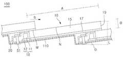
도 3은 상기 백라이트 유닛(100)의 단면도이고, 도 4는 상기 백라이트 유닛(100)의 사시도이고, 도 5는 상기 백라이트 유닛(100)의 평면도이다.3 is a cross-sectional view of the
도 3 내지 도 5를 참조하면, 상기 백라이트 유닛(100)은 다수의 광학 어셈블리(10)들을 포함한다. 상기 다수의 광학 어셈블리(10)들은 제1 각도(θ)로 기울어져 제1 영역(M)이 중첩되도록 제2 방향(b)으로 배치될 수 있다.3 to 5, the
상기 광학 어셈블리(10)들은 각각 도광판(15)과, 상기 도광판(15)의 일 측에 배치된 발광모듈부(13)와, 상기 도광판(15) 및 상기 발광모듈부(13)를 고정하는 사이드 커버(20)를 포함할 수 있다.Each of the
상기 발광모듈부(13)는 상기 도광판(15)의 일 측에 배치되어, 상기 도광판(15)에 광을 제공한다. 상기 발광모듈부(13)는 기판(12) 및 상기 기판(12) 상에 어레이(array)를 이루어 탑재되는 다수의 발광 소자(11)를 포함할 수 있다.The light emitting
상기 기판(12)은 인쇄회로기판(PCB : Printed Circuit Board)일 수 있으며, 예를 들어, 메탈 코어 PCB, FR-4 PCB, 일반 PCB, 플렉시블 기판 등으로 이루어질 수 있다.The
또한, 상기 발광 소자(11)는 발광 다이오드(LED) 일 수 있으며, 상기 발광 다이오드는 예를 들어, 적색, 녹색, 청색 또는 백색의 광을 발광하는 적색, 녹색, 청색 또는 백색 발광 다이오드일 수 있으나, 이에 대해 한정하지는 않는다.In addition, the
한편, 도시되지는 않았지만, 상기 발광모듈부(13)와 상기 도광판(15) 사이에는 광가이드 부재(미도시)가 형성될 수 있다. 상기 광가이드부재(미도시)는 상기 도광판(15)과 동일한 재질로 형성될 수 있으며, 상기 발광모듈부(13)와 상기 도광판(15) 사이의 공간에 형성되어, 상기 발광모듈부(13)로부터 방출되는 광이 효과적으로 상기 도광판(15)으로 가이드될 수 있도록 할 수 있다.Although not shown, an optical guide member (not shown) may be formed between the light emitting
또한, 도시되지는 않았지만, 상기 발광모듈부(13)와 상기 도광판(15) 사이에는 광여기 필름(PLF : Phosphor Luminescent Film)이 형성될 수 있다.In addition, although not shown, a photo-excited film (PLF: Phosphor Luminescent Film) may be formed between the light emitting
상기 광여기 필름(PLF)은 형광체를 포함하는 필름으로써, 상기 형광체는 상기 발광모듈부(13)에서 방출되는 제1빛에 의해 여기되어 제2빛을 생성할 수 있다.The photoexcited film (PLF) is a film containing a phosphor, the phosphor may be excited by the first light emitted from the light emitting
예를 들어, 상기 발광모듈부(13)에서 방출되는 빛이 청색(blue)이고, 상기 형광체가 상기 청색 빛에 의해 여기되어 황색 빛을 생성하는 황색 형광체인 경우, 결과적으로 두 가지 빛이 혼색되어 백색의 빛이 상기 도광판(15)에 제공될 수 있다. 다만, 이에 대해 한정하지는 않는다.For example, when the light emitted from the light emitting
상기 도광판(15)은 상기 발광모듈부(13)로부터 제공받은 광을 면광원화 하여, 상기 표시 패널(210)에 제공한다.The
상기 도광판(15)은 투명한 재질로 이루어지며, 예를 들어, PMMA(polymethyl metaacrylate)와 같은 아크릴 수지 계열, PET(polyethylene terephthlate), PC(poly carbonate), COC(cycloolefin copolymer) 및 PEN(polyethylene naphthalate) 수지 중 하나를 포함할 수 있다.The
상기 도광판(15)은 제1 방향(a)으로 길게 연장된 직사각형 형태일 수 있으나, 이에 대해 한정하지는 않는다. 또한, 상기 도광판(15)은 전 영역에 대하여 실질적으로 일정한 두께를 가질 수 있다.The
상기 도광판(15)의 상면 또는 하면에는 산란 패턴(미도시)이 형성될 수 있다. 상기 산란 패턴은 소정의 패턴으로 이루어져 입사되는 광을 난반사 시킴으로써 상기 도광판(15) 전면에서 광 균일성을 향상시키는 역할을 한다.A scattering pattern (not shown) may be formed on the top or bottom surface of the
상기 도광판(15)은 압출 성형법에 의해 제조될 수 있다. 따라서, 상기 도광판(15)이 상기 제1 방향(a)으로 예를 들어, 1 미터(meter) 이상 길게 연장되더라도 용이하게 제조될 수 있으며, 일정한 두께를 가지도록 제조될 수 있다. 또한, 상기 압출 성형 후에 상기 도광판(15)의 상면 또는 하면에 상기 산란 패턴(미도시)을 형성할 수 있다.The
상기 도광판(15)의 하면에는 반사 부재(17)가 형성될 수 있다. 따라서, 상기 발광모듈부(13)로부터 측면 입사된 광이 상기 도광판(15) 내부에서 가이드되어 상기 반사 부재(17)에 반사된 다음 상기 도광판(15)의 상면으로 출사될 수 있다.A
또한, 상기 반사 부재(17)는 중첩되어 배치된 다른 광학 어셈블리(10)에서 발생된 광에 의한 간섭을 차단하는 역할을 할 수도 있다.In addition, the
도 4를 참조하면, 상기 백라이트 유닛(100)의 출사면에 노출되는 상기 도광판(15)의 노출 측면(19)에는 표면 처리를 하여, 상기 노출 측면(19)을 통해 빛이 새어나가 출사면에 일(ㅡ)자 무늬가 형성되는 것을 방지할 수 있다.Referring to FIG. 4, the exposed
상기 노출 측면(19)은 상기 도광판(15)의 측면 중 상기 발광모듈부(13)가 배치된 측면의 반대 측면 일 수 있다.The exposed
상기 표면 처리는 예를 들어, 검정색, 흰색, 회색 중 적어도 하나의 색을 가지는 PSR(Photo Solder Resist) 잉크 등에 의한 도색을 포함할 수 있다. 다만, 이에 대해 한정하지는 않는다.The surface treatment may include, for example, painting with PSR (Photo Solder Resist) ink having a color of at least one of black, white, and gray. However, this is not limitative.
한편, 상기 일자 무늬가 형성되는 것을 방지하기 위해, 상기 백라이트 유닛(100) 상에는 확산 플레이트가 배치될 수도 있다. 이에 대해서는 후술한다.On the other hand, in order to prevent the date pattern is formed, a diffusion plate may be disposed on the
상기 사이드 커버(20)는 상기 도광판(15)의 일 측에 형성될 수 있으며, 내부에 상기 발광모듈부(13)를 수납할 수 있다. 이에 따라, 상기 사이드 커버(20)는 상기 도광판(15) 및 상기 발광모듈부(13)를 고정하고, 상기 백라이트 유닛(100)을 상기 바텀 커버(110)에 스크류 등의 체결 나사(51)에 의해 결합할 수 있다.The side cover 20 may be formed at one side of the
상기 사이드 커버(20)는 플라스틱 또는 금속 재질로 이루어질 수 있다. 다만, 상기 사이드 커버(20)의 형태 및 재질에 의해 한정하지는 않으며, 상기 백라이트 유닛(100)의 설계에 따라 다양하게 변형될 수 있다.The side cover 20 may be made of plastic or metal. However, the present invention is not limited to the shape and material of the
상기 광학 어셈블리(10)들은 상기 도광판(15)의 일부 영역, 상기 발광모듈부(13) 및 상기 사이드 커버(20)를 포함하는 제1 영역(M)과, 상기 제1 영역(M)에서 제공받은 빛을 전면으로 발산시키는 제2 영역(N)을 포함한다.The
상기 광학 어셈블리(10)들은 상기 제1 영역(M)이 중첩되도록 제2 방향(b)으로 다수 개가 배치될 수 있다. 즉, 상기 제1 영역(M)은 인근에 배치되는 광학 어셈 블리(10)의 제2 영역(N) 하부에 배치될 수 있다. 따라서, 상기 광학 어셈블리(10)들의 상기 제1 영역(M)들은 평면 상에서 관찰되지 않을 수 있다. 다만, 상기 백라이트 유닛(100)의 일측 모서리에 배치된 광학 어셈블리(10)의 제1 영역(M)은 중첩되지 않으므로 평면 상에 드러날 수 있다.A plurality of
상기 광학 어셈블리(10)들은 도 4 및 도 5에 도시된 것처럼, 제1 방향(a)으로 길게 연장된 직사각형 형태일 수 있으나, 이에 대해 한정하지는 않는다. 상기 광학 어셈블리(10)들은 이와 같은 형태를 가지므로, 상기 제2 방향(b)으로 다수 개가 배치됨으로써, 상기 백라이트 유닛(100)을 구성할 수 있다. 예를 들어, 상기 백라이트 유닛(100)은 상기 다수의 광학 어셈블리(10)들이 1×n의 배열로 배치되어 형성될 수 있다.4 and 5, the
각각의 상기 광학 어셈블리(10)들은 독립적인 어셈블리로 제작될 수 있으며, 근접 배치됨으로써 모듈형 백라이트 유닛을 형성할 수 있다. 이와 같은 모듈형 백라이트 유닛은 백라이트 수단으로서 상기 표시 패널(210)에 광을 제공할 수 있다.Each of the
실시예에 따른 백라이트 유닛(100)은 전체 구동 방식 또는 로컬 디밍(local dimming), 임펄시브(impulsive) 등과 같은 부분 구동 방식으로 구동될 수 있다.The
상기 백라이트 유닛(100)이 예를 들어, 상기 로컬 디밍 방식으로 구동될 경우, 상기 광학 어셈블리(10)들에 대응하여 상기 표시 패널(210)은 다수의 분할 영역을 가질 수 있으며, 상기 분할 영역들의 그레이 레벨의 피크값 또는 색 좌표 신호에 따라 각각의 상기 광학 어셈블리(10) 별로 휘도를 조절할 수 있다.When the
즉, 상기 백라이트 유닛(100)이 부분 구동 방식으로 동작되는 경우, 분할 구 동 영역의 휘도를 영상 신호의 휘도와 연계하여 영상의 검은색 부분은 휘도를 감소시키고 밝은 부분은 휘도를 증가시킴으로써, 명암비 및 선명도를 향상시킬 수 있고, 소비 전력을 감소시켜 비용 절감의 효과가 있다.That is, when the
도 6는 상기 다수의 광학 어셈블리(10)의 도광판(15)들 만을 간단하게 도시한 도면이다.FIG. 6 is a diagram schematically illustrating only the
도 3 및 도 6를 참조하면, 상기 광학 어셈블리(10)들은 제1 각도(θ)로 기울어져, 상기 제2 방향(b)으로 다수 개가 배치되므로, 상기 백라이트 유닛(100)의 두께(L)는 <수학식 1> 과 같이, 상기 제1 각도(θ) 및 상기 도광판(15)의 너비(A)와 두께(B)에 따라 결정될 수 있다.3 and 6, since the plurality of

또한, 상기 다수의 광학 어셈블리(10)들이 서로 중첩되는 중첩거리(x)도 <수학식 2>와 같이, 상기 제1 각도(θ) 및 상기 도광판(15)의 너비(A)와 두께(B)에 따라 결정될 수 있다.In addition, the overlapping distance (x) at which the plurality of

상기 광학 어셈블리(10)들은 상기 제1 각도(θ)로 기울어져 다수 개가 제2 방향(b)을 따라 배치되므로, 상기 백라이트 유닛(100)의 두께(L)를 감소시킬 수 있다.Since the plurality of
상기 제1 각도(θ)는 0°를 초과하고 90°미만 일 수 있으며, 바람직하게는 0.1°내지 30°일 수 있으나, 이에 대해 한정하지는 않는다.The first angle θ may be greater than 0 ° and less than 90 °, and preferably 0.1 ° to 30 °, but is not limited thereto.
상기 광학 어셈블리(10)들 각각은 에지(Edge)형 백라이트 방식으로 구동이 이루어지며, 상기 광학 어셈블리(10)들은 다시 하나의 광원으로서 동작하여 상기 표시 패널(210)에 직하형 백라이트 방식으로 광을 제공함으로써 백라이트 유닛을 형성할 수 있다. 따라서, 상기 발광 소자(11)들이 화면 상에 핫 스팟(hot spot)으로 관찰되는 문제를 해소할 수 있으며, 상기 도광판(15)의 두께를 감소시키고 광학 필름들의 수를 줄일 수 있어 상기 백라이트 유닛(100)의 슬림화를 구현할 수 있다.Each of the
도 2를 참조하면, 상기 백라이트 유닛(100) 상에는 상기 광학 시트(220)가 배치될 수 있다. 이때, 상기 광학 시트(220)는 상기 다수의 광학 어셈블리(10)와 선 접촉할 수 있다.Referring to FIG. 2, the
상기 다수의 광학 어셈블리(10)는 상기 제1 각도(θ)로 기울어져 다수 개가 제2 방향(b)을 따라 배치되고, 상기 도광판(15)은 일정한 두께를 가지고 제1 방 향(a)으로 연장된 직사각형 형태이므로, 상기 백라이트 유닛(100) 최상면은 다수의 선으로 이루어지게 된다. 따라서, 상기 광학 시트(220)는 상기 백라이트 유닛(100) 상에 선 접촉에 의해 배치될 수 있다.The plurality of
다만, 이에 대해 한정하지는 않으며, 상기 광학 시트(220)는 상기 백라이트 유닛(100) 상에 일정 간격을 두고 배치될 수도 있다.However, the present invention is not limited thereto, and the
또한, 상기 다수의 광학 어셈블리(10)는 상기 제1 각도(θ)로 기울어져 다수 개가 제2 방향(b)을 따라 배치되므로, 상기 다수의 광학 어셈블리(10)들은 상기 표시 패널(210)에 대해 상기 제1 각도(θ)를 가지도록 기울어져 배치된다.In addition, since the plurality of
실시예에 따른 백라이트 유닛(100)은 상기 광학 어셈블리(10)들을 조립하여 백라이트 유닛(100)을 제조하는 공정이 간단하고 조립 과정에서 발생할 수 있는 로스(loss)를 최소화하여 생산성을 향상시킬 수 있다. 또한, 백라이트 유닛(100)의 조립 과정에서 발생할 수 있는 도광판 스크래치 등에 의한 불량 발생을 줄이고 광학적 무라(mura) 발생을 개선시킬 수 있어 공정 신뢰성을 향상시키고 품질을 향상시킬 수 있는 효과가 있다.The
실시예에 따른 백라이트 유닛(100)은 상기 광학 어셈블리(10)를 압출 성형에 의해 제조될 수 있으므로, 제조 공정이 간단하여 대량 생산이 용이하며, 다양한 사이즈의 백라이트 유닛에 적용할 수 있다.Since the
실시예에 따른 백라이트 유닛(100)의 광학 어셈블리(10)들 중 어느 하나에 불량이 발생할 경우 전체의 백라이트 유닛(100)을 교체할 필요 없이 불량이 발생한 광학 어셈블리만 교체하면 되므로 교체 작업이 용이하고 부품 교체 비용이 절감되 는 효과가 있다.When a failure occurs in any one of the
실시예에 따른 광학 어셈블리(10) 및 이를 구비하는 백라이트 유닛(100)은 외부로부터의 충격 또는 환경 변화에 대해 강건하고 내구성이 뛰어난 효과가 있다.The
실시예에 따른 백라이트 유닛(100)의 광학 어셈블리(10)들은 인접한 광학 어셈블리(10)들의 일부가 서로 중첩되어 배치되고, 상기 광학 어셈블리(10)의 노출 측면(19)에 표면 처리를 실시하므로, 상기 광학 어셈블리(10)들 경계에서의 휘선 또는 암선 발생을 개선시키고 광의 균일성 확보가 가능한 효과가 있다.Since the
실시예에 따른 백라이트 유닛(100)은 대형 표시 패널에 적용이 용이하다. 또한, 실시예는 백라이트 유닛 및 디스플레이 장치의 슬림화에 유리한 효과가 있다.The
도 7 및 도 8은 확산 플레이트(30)를 도시한 도면이다.7 and 8 show the
도 7 및 도 8을 참조하면, 상기 확산 플레이트(30)는 상기 백라이트 유닛(100)과 상기 광학 시트(220) 사이에 배치되어, 상기 백라이트 유닛(100)의 출사면에 일(ㅡ)자 무늬가 형성되는 것을 방지할 수 있다.Referring to FIGS. 7 and 8, the
상기 확산 플레이트(30)에는 확산 패턴(31)이 형성될 수 있다. 상기 확산 패턴(31)은 상기 백라이트 유닛(100)의 상기 노출 측면(19)에 대응되는 부분에 형성될 수 있다.A
상기 확산 패턴(31)은 예를 들어, 도 7의 볼록 패턴(31), 도 8의 요철 패턴(31a)일 수 있으나, 이에 대해 한정하지는 않는다.The
상기 확산 플레이트(30)는 예를 들어, 압출 성형에 의해 형성될 수 있으나, 이에 대해 한정하지는 않는다. 또한, 상기 확산 패턴(31)은 상기 압출 성형 과정에서, 롤러(Roller)에 의해 상기 확산 플레이트(30)를 압출하는 것과 동시에 형성될 수 있다.The
상기 확산 플레이트(30)는 예를 들어, PMMA(polymethyl metaacrylate)와 같은 아크릴 수지 계열, PET(polyethylene terephthlate), PC(poly carbonate), COC(cycloolefin copolymer) 및 PEN(polyethylene naphthalate) 수지 중 어느 하나로 형성될 수 있다.The
상기 확산 플레이트(30)가 상기 백라이트 유닛(100)과 상기 광학 시트(220) 사이에 배치되는 경우, 상기 확산 플레이트(30)는 상기 백라이트 유닛(100)과 선 접촉 할 수 있다. 다만, 상기 확산 플레이트(30)는 형성되지 않을 수도 있다.When the
이상에서 실시예들에 설명된 특징, 구조, 효과 등은 본 발명의 적어도 하나의 실시예에 포함되며, 반드시 하나의 실시예에만 한정되는 것은 아니다. 나아가, 각 실시예에서 예시된 특징, 구조, 효과 등은 실시예들이 속하는 분야의 통상의 지식을 가지는 자에 의해 다른 실시예들에 대해서도 조합 또는 변형되어 실시 가능하다. 따라서 이러한 조합과 변형에 관계된 내용들은 본 발명의 범위에 포함되는 것으로 해석되어야 할 것이다.Features, structures, effects, and the like described in the above embodiments are included in at least one embodiment of the present invention, and are not necessarily limited to only one embodiment. Furthermore, the features, structures, effects, and the like illustrated in the embodiments may be combined or modified with respect to other embodiments by those skilled in the art to which the embodiments belong. Therefore, it should be understood that the present invention is not limited to these combinations and modifications.
또한, 이상에서 실시예를 중심으로 설명하였으나 이는 단지 예시일 뿐 본 발명을 한정하는 것이 아니며, 본 발명이 속하는 분야의 통상의 지식을 가진 자라면 본 실시예의 본질적인 특성을 벗어나지 않는 범위에서 이상에 예시되지 않은 여러 가지의 변형과 응용이 가능함을 알 수 있을 것이다. 예를 들어, 실시예에 구체적으로 나타난 각 구성 요소는 변형하여 실시할 수 있는 것이다. 그리고 이러한 변형과 응용에 관계된 차이점들은 첨부된 청구 범위에서 규정하는 본 발명의 범위에 포함되는 것으로 해석되어야 할 것이다.In addition, the above description has been made with reference to the embodiment, which is merely an example, and is not intended to limit the present invention. It will be appreciated that various modifications and applications are possible. For example, each component specifically shown in the embodiment can be modified. And differences relating to such modifications and applications will have to be construed as being included in the scope of the invention defined in the appended claims.
도 1 내지 도 8은 실시예에 따른 백라이트 유닛 및 이를 이용한 디스플레이 장치에 관한 것이다.1 to 8 are related to a backlight unit and a display device using the same according to an embodiment.
Claims (20)
Translated fromKorean

Priority Applications (4)
| Application Number | Priority Date | Filing Date | Title |
|---|---|---|---|
| KR1020090079030AKR101047601B1 (en) | 2009-08-26 | 2009-08-26 | Backlight unit and display device using same |
| EP10173784AEP2299301A1 (en) | 2009-08-26 | 2010-08-24 | Backlight unit and display device using the same |
| US12/868,462US20110051048A1 (en) | 2009-08-26 | 2010-08-25 | Backlight unit and display device using the same |
| CN2010102656958ACN102003641A (en) | 2009-08-26 | 2010-08-26 | Backlight unit and display apparatus using thereof |
Applications Claiming Priority (1)
| Application Number | Priority Date | Filing Date | Title |
|---|---|---|---|
| KR1020090079030AKR101047601B1 (en) | 2009-08-26 | 2009-08-26 | Backlight unit and display device using same |
Publications (2)
| Publication Number | Publication Date |
|---|---|
| KR20110021314A KR20110021314A (en) | 2011-03-04 |
| KR101047601B1true KR101047601B1 (en) | 2011-07-07 |
Family
ID=43500556
Family Applications (1)
| Application Number | Title | Priority Date | Filing Date |
|---|---|---|---|
| KR1020090079030AExpired - Fee RelatedKR101047601B1 (en) | 2009-08-26 | 2009-08-26 | Backlight unit and display device using same |
Country Status (4)
| Country | Link |
|---|---|
| US (1) | US20110051048A1 (en) |
| EP (1) | EP2299301A1 (en) |
| KR (1) | KR101047601B1 (en) |
| CN (1) | CN102003641A (en) |
Families Citing this family (5)
| Publication number | Priority date | Publication date | Assignee | Title |
|---|---|---|---|---|
| CN102621739A (en)* | 2012-03-31 | 2012-08-01 | 深圳市华星光电技术有限公司 | Liquid crystal display device and manufacturing method thereof |
| CN105022192A (en)* | 2015-08-10 | 2015-11-04 | 苏州固特斯电子科技有限公司 | High concentration photovoltaic liquid crystal display module |
| CN106773325B (en)* | 2017-03-14 | 2020-05-19 | 深圳市华星光电技术有限公司 | Local dimming type ultrathin backlight module and display device |
| KR102657039B1 (en)* | 2018-12-19 | 2024-04-11 | 엘지디스플레이 주식회사 | Display device |
| CN115995221B (en)* | 2023-03-23 | 2023-06-23 | 惠科股份有限公司 | Display device and electronic equipment |
Citations (4)
| Publication number | Priority date | Publication date | Assignee | Title |
|---|---|---|---|---|
| KR200309634Y1 (en) | 2002-05-03 | 2003-04-03 | 주식회사 파인옵틱스 | Display system having backlight unit |
| KR20050076848A (en)* | 2004-01-24 | 2005-07-28 | 삼성전자주식회사 | Back light unit |
| KR100784023B1 (en) | 2006-03-20 | 2007-12-07 | 엘지이노텍 주식회사 | Backlight unit and liquid crystal display device having same |
| KR20080059719A (en)* | 2006-12-26 | 2008-07-01 | 엘지디스플레이 주식회사 | Backlight unit and liquid crystal display module having same |
Family Cites Families (26)
| Publication number | Priority date | Publication date | Assignee | Title |
|---|---|---|---|---|
| KR100654220B1 (en)* | 1999-08-03 | 2006-12-05 | 삼성전자주식회사 | LCD Display |
| JP2001312916A (en)* | 2000-02-24 | 2001-11-09 | Sony Corp | Surface light source device |
| JP4863576B2 (en)* | 2001-06-06 | 2012-01-25 | セイコーインスツル株式会社 | Liquid crystal display |
| JP2004206916A (en)* | 2002-12-24 | 2004-07-22 | Yoshihiro Sakai | Planar light source |
| KR20040094053A (en)* | 2003-05-01 | 2004-11-09 | 주식회사 우영 | Back light for display device |
| JP4081448B2 (en)* | 2004-01-14 | 2008-04-23 | シャープ株式会社 | Liquid crystal display |
| JP4386749B2 (en)* | 2004-02-16 | 2009-12-16 | シチズン電子株式会社 | Planar light source |
| KR101096720B1 (en)* | 2004-05-28 | 2011-12-22 | 엘지디스플레이 주식회사 | Apparatus and method for driving liquid crystal display device |
| KR101065654B1 (en)* | 2004-06-15 | 2011-09-20 | 삼성전자주식회사 | Back light assembly and display device having same |
| TWI293702B (en)* | 2005-03-17 | 2008-02-21 | Au Optronics Corp | Backlight modules |
| KR20080005198A (en)* | 2005-04-12 | 2008-01-10 | 테이진 카세이 가부시키가이샤 | Resin Sheet and Direct Backlight Unit and Direct Backlit Liquid Crystal Display |
| KR100687926B1 (en)* | 2005-06-13 | 2007-02-27 | 삼성전자주식회사 | LCD Display |
| JP2007095662A (en)* | 2005-09-02 | 2007-04-12 | Mitsubishi Electric Corp | Surface light source device |
| TWI321682B (en)* | 2005-10-14 | 2010-03-11 | Innolux Display Corp | Liquid cyrstal display and method for assebling the same |
| US7891852B2 (en)* | 2005-10-17 | 2011-02-22 | Koninklijke Philips Electronics Nv | Illumination system using phosphor remote from light source |
| TW200745680A (en)* | 2006-04-19 | 2007-12-16 | Omron Tateisi Electronics Co | Diffuser plate and surface light source device |
| TWI318701B (en)* | 2006-08-18 | 2009-12-21 | Innolux Display Corp | Liquid crystal display device |
| US7907804B2 (en)* | 2007-12-19 | 2011-03-15 | Oree, Inc. | Elimination of stitch artifacts in a planar illumination area |
| JP2009163016A (en)* | 2008-01-07 | 2009-07-23 | Masaki Hamaguchi | Thin type external illumination signboard |
| CN101896765B (en)* | 2008-02-05 | 2012-07-04 | 夏普株式会社 | Lighting device and liquid crystal display device |
| JP2010021131A (en)* | 2008-06-09 | 2010-01-28 | Hitachi Ltd | Display device and backlight unit used for the same |
| KR20100020652A (en)* | 2008-08-13 | 2010-02-23 | 삼성전기주식회사 | Edge type back light unit module |
| TW201024856A (en)* | 2008-12-25 | 2010-07-01 | Chunghwa Picture Tubes Ltd | Backlight module and display module thereof |
| KR101628366B1 (en)* | 2009-07-06 | 2016-06-08 | 엘지전자 주식회사 | optical assembly, backlight unit having the same, and display apparatus thereof |
| KR20110020055A (en)* | 2009-08-21 | 2011-03-02 | 엘지이노텍 주식회사 | Backlight unit |
| TW201120522A (en)* | 2009-12-02 | 2011-06-16 | Dynascan Technology Corp | Stack combinational backlight panel used in display and display having the same. |
- 2009
- 2009-08-26KRKR1020090079030Apatent/KR101047601B1/ennot_activeExpired - Fee Related
- 2010
- 2010-08-24EPEP10173784Apatent/EP2299301A1/ennot_activeWithdrawn
- 2010-08-25USUS12/868,462patent/US20110051048A1/ennot_activeAbandoned
- 2010-08-26CNCN2010102656958Apatent/CN102003641A/enactivePending
Patent Citations (4)
| Publication number | Priority date | Publication date | Assignee | Title |
|---|---|---|---|---|
| KR200309634Y1 (en) | 2002-05-03 | 2003-04-03 | 주식회사 파인옵틱스 | Display system having backlight unit |
| KR20050076848A (en)* | 2004-01-24 | 2005-07-28 | 삼성전자주식회사 | Back light unit |
| KR100784023B1 (en) | 2006-03-20 | 2007-12-07 | 엘지이노텍 주식회사 | Backlight unit and liquid crystal display device having same |
| KR20080059719A (en)* | 2006-12-26 | 2008-07-01 | 엘지디스플레이 주식회사 | Backlight unit and liquid crystal display module having same |
Also Published As
| Publication number | Publication date |
|---|---|
| CN102003641A (en) | 2011-04-06 |
| US20110051048A1 (en) | 2011-03-03 |
| KR20110021314A (en) | 2011-03-04 |
| EP2299301A1 (en) | 2011-03-23 |
Similar Documents
| Publication | Publication Date | Title |
|---|---|---|
| US9366893B2 (en) | Liquid crystal display device | |
| US8432525B2 (en) | Backlight unit and liquid crystal display device having the same | |
| KR101395572B1 (en) | Liquid crystal display device module | |
| KR20160022224A (en) | Light guide plate and backlight unit having the same | |
| KR20100078298A (en) | Backlight unit and liquid crystal display device module including the same | |
| KR20110003777A (en) | Optical assembly, backlight unit and display device having same | |
| KR20100097515A (en) | Backlight unit for liquid crystal display device module | |
| KR102222297B1 (en) | Reflector for uniform brightness and liquid crystal display device having thereof | |
| US8506106B2 (en) | Backlight unit and display apparatus including the same | |
| CN100421008C (en) | Backlight unit and liquid crystal display using same | |
| US20240411179A1 (en) | Display module and display device | |
| KR101047601B1 (en) | Backlight unit and display device using same | |
| KR101591336B1 (en) | Liquid crystal display | |
| KR20100094158A (en) | Backlight unit and liquid crystal display device having the same | |
| KR20110014869A (en) | Backlight unit and display device using same | |
| KR101992891B1 (en) | Backlight unit and liquid crystal display device using the same | |
| KR20110041825A (en) | Backlight unit and liquid crystal display device having same | |
| KR20120047715A (en) | Light emitting diode, back light unit and liquid crystal display device having thereof | |
| KR20170064106A (en) | Backlight unit and display device | |
| KR20110012547A (en) | Backlight unit and display device using same | |
| US8057088B2 (en) | Backlight unit and liquid crystal display device including the same | |
| KR101047704B1 (en) | Backlight unit and display device with optical assembly | |
| KR101064088B1 (en) | Backlight unit and display device with optical assembly | |
| KR100889222B1 (en) | Light guide plate of liquid crystal display device and manufacturing method thereof | |
| KR101072052B1 (en) | optical assembly, backlight unit having the same, and display apparatus thereof |
Legal Events
| Date | Code | Title | Description |
|---|---|---|---|
| A201 | Request for examination | ||
| PA0109 | Patent application | St.27 status event code:A-0-1-A10-A12-nap-PA0109 | |
| PA0201 | Request for examination | St.27 status event code:A-1-2-D10-D11-exm-PA0201 | |
| R18-X000 | Changes to party contact information recorded | St.27 status event code:A-3-3-R10-R18-oth-X000 | |
| A302 | Request for accelerated examination | ||
| PA0302 | Request for accelerated examination | St.27 status event code:A-1-2-D10-D17-exm-PA0302 St.27 status event code:A-1-2-D10-D16-exm-PA0302 | |
| D13-X000 | Search requested | St.27 status event code:A-1-2-D10-D13-srh-X000 | |
| D14-X000 | Search report completed | St.27 status event code:A-1-2-D10-D14-srh-X000 | |
| E902 | Notification of reason for refusal | ||
| PE0902 | Notice of grounds for rejection | St.27 status event code:A-1-2-D10-D21-exm-PE0902 | |
| P11-X000 | Amendment of application requested | St.27 status event code:A-2-2-P10-P11-nap-X000 | |
| P13-X000 | Application amended | St.27 status event code:A-2-2-P10-P13-nap-X000 | |
| E902 | Notification of reason for refusal | ||
| PE0902 | Notice of grounds for rejection | St.27 status event code:A-1-2-D10-D21-exm-PE0902 | |
| E13-X000 | Pre-grant limitation requested | St.27 status event code:A-2-3-E10-E13-lim-X000 | |
| P11-X000 | Amendment of application requested | St.27 status event code:A-2-2-P10-P11-nap-X000 | |
| P13-X000 | Application amended | St.27 status event code:A-2-2-P10-P13-nap-X000 | |
| PG1501 | Laying open of application | St.27 status event code:A-1-1-Q10-Q12-nap-PG1501 | |
| E90F | Notification of reason for final refusal | ||
| PE0902 | Notice of grounds for rejection | St.27 status event code:A-1-2-D10-D21-exm-PE0902 | |
| P11-X000 | Amendment of application requested | St.27 status event code:A-2-2-P10-P11-nap-X000 | |
| P13-X000 | Application amended | St.27 status event code:A-2-2-P10-P13-nap-X000 | |
| E701 | Decision to grant or registration of patent right | ||
| PE0701 | Decision of registration | St.27 status event code:A-1-2-D10-D22-exm-PE0701 | |
| GRNT | Written decision to grant | ||
| PR0701 | Registration of establishment | St.27 status event code:A-2-4-F10-F11-exm-PR0701 | |
| PR1002 | Payment of registration fee | St.27 status event code:A-2-2-U10-U11-oth-PR1002 Fee payment year number:1 | |
| PG1601 | Publication of registration | St.27 status event code:A-4-4-Q10-Q13-nap-PG1601 | |
| FPAY | Annual fee payment | Payment date:20140609 Year of fee payment:4 | |
| PR1001 | Payment of annual fee | St.27 status event code:A-4-4-U10-U11-oth-PR1001 Fee payment year number:4 | |
| PN2301 | Change of applicant | St.27 status event code:A-5-5-R10-R13-asn-PN2301 St.27 status event code:A-5-5-R10-R11-asn-PN2301 | |
| FPAY | Annual fee payment | Payment date:20150605 Year of fee payment:5 | |
| PR1001 | Payment of annual fee | St.27 status event code:A-4-4-U10-U11-oth-PR1001 Fee payment year number:5 | |
| FPAY | Annual fee payment | Payment date:20160607 Year of fee payment:6 | |
| PR1001 | Payment of annual fee | St.27 status event code:A-4-4-U10-U11-oth-PR1001 Fee payment year number:6 | |
| R18-X000 | Changes to party contact information recorded | St.27 status event code:A-5-5-R10-R18-oth-X000 | |
| FPAY | Annual fee payment | Payment date:20170605 Year of fee payment:7 | |
| PR1001 | Payment of annual fee | St.27 status event code:A-4-4-U10-U11-oth-PR1001 Fee payment year number:7 | |
| PR1001 | Payment of annual fee | St.27 status event code:A-4-4-U10-U11-oth-PR1001 Fee payment year number:8 | |
| R18-X000 | Changes to party contact information recorded | St.27 status event code:A-5-5-R10-R18-oth-X000 | |
| PC1903 | Unpaid annual fee | St.27 status event code:A-4-4-U10-U13-oth-PC1903 Not in force date:20190702 Payment event data comment text:Termination Category : DEFAULT_OF_REGISTRATION_FEE | |
| R18-X000 | Changes to party contact information recorded | St.27 status event code:A-5-5-R10-R18-oth-X000 | |
| PC1903 | Unpaid annual fee | St.27 status event code:N-4-6-H10-H13-oth-PC1903 Ip right cessation event data comment text:Termination Category : DEFAULT_OF_REGISTRATION_FEE Not in force date:20190702 | |
| PN2301 | Change of applicant | St.27 status event code:A-5-5-R10-R13-asn-PN2301 St.27 status event code:A-5-5-R10-R11-asn-PN2301 |