KR101045371B1 - Micro pattern formation method using double patterning - Google Patents
Micro pattern formation method using double patterningDownload PDFInfo
- Publication number
- KR101045371B1 KR101045371B1KR1020080131678AKR20080131678AKR101045371B1KR 101045371 B1KR101045371 B1KR 101045371B1KR 1020080131678 AKR1020080131678 AKR 1020080131678AKR 20080131678 AKR20080131678 AKR 20080131678AKR 101045371 B1KR101045371 B1KR 101045371B1
- Authority
- KR
- South Korea
- Prior art keywords
- mask
- pattern
- layer
- patterns
- forming
- Prior art date
- Legal status (The legal status is an assumption and is not a legal conclusion. Google has not performed a legal analysis and makes no representation as to the accuracy of the status listed.)
- Expired - Fee Related
Links
Images


Classifications
- G—PHYSICS
- G03—PHOTOGRAPHY; CINEMATOGRAPHY; ANALOGOUS TECHNIQUES USING WAVES OTHER THAN OPTICAL WAVES; ELECTROGRAPHY; HOLOGRAPHY
- G03F—PHOTOMECHANICAL PRODUCTION OF TEXTURED OR PATTERNED SURFACES, e.g. FOR PRINTING, FOR PROCESSING OF SEMICONDUCTOR DEVICES; MATERIALS THEREFOR; ORIGINALS THEREFOR; APPARATUS SPECIALLY ADAPTED THEREFOR
- G03F7/00—Photomechanical, e.g. photolithographic, production of textured or patterned surfaces, e.g. printing surfaces; Materials therefor, e.g. comprising photoresists; Apparatus specially adapted therefor
- G03F7/70—Microphotolithographic exposure; Apparatus therefor
- G03F7/70425—Imaging strategies, e.g. for increasing throughput or resolution, printing product fields larger than the image field or compensating lithography- or non-lithography errors, e.g. proximity correction, mix-and-match, stitching or double patterning
- G03F7/70466—Multiple exposures, e.g. combination of fine and coarse exposures, double patterning or multiple exposures for printing a single feature
- H—ELECTRICITY
- H01—ELECTRIC ELEMENTS
- H01L—SEMICONDUCTOR DEVICES NOT COVERED BY CLASS H10
- H01L21/00—Processes or apparatus adapted for the manufacture or treatment of semiconductor or solid state devices or of parts thereof
- H01L21/02—Manufacture or treatment of semiconductor devices or of parts thereof
- H01L21/027—Making masks on semiconductor bodies for further photolithographic processing not provided for in group H01L21/18 or H01L21/34
- H01L21/033—Making masks on semiconductor bodies for further photolithographic processing not provided for in group H01L21/18 or H01L21/34 comprising inorganic layers
- H01L21/0334—Making masks on semiconductor bodies for further photolithographic processing not provided for in group H01L21/18 or H01L21/34 comprising inorganic layers characterised by their size, orientation, disposition, behaviour, shape, in horizontal or vertical plane
- H01L21/0338—Process specially adapted to improve the resolution of the mask
- H—ELECTRICITY
- H01—ELECTRIC ELEMENTS
- H01L—SEMICONDUCTOR DEVICES NOT COVERED BY CLASS H10
- H01L21/00—Processes or apparatus adapted for the manufacture or treatment of semiconductor or solid state devices or of parts thereof
- H01L21/02—Manufacture or treatment of semiconductor devices or of parts thereof
- H01L21/04—Manufacture or treatment of semiconductor devices or of parts thereof the devices having potential barriers, e.g. a PN junction, depletion layer or carrier concentration layer
- H01L21/18—Manufacture or treatment of semiconductor devices or of parts thereof the devices having potential barriers, e.g. a PN junction, depletion layer or carrier concentration layer the devices having semiconductor bodies comprising elements of Group IV of the Periodic Table or AIIIBV compounds with or without impurities, e.g. doping materials
- H01L21/30—Treatment of semiconductor bodies using processes or apparatus not provided for in groups H01L21/20 - H01L21/26
- H01L21/31—Treatment of semiconductor bodies using processes or apparatus not provided for in groups H01L21/20 - H01L21/26 to form insulating layers thereon, e.g. for masking or by using photolithographic techniques; After treatment of these layers; Selection of materials for these layers
- H01L21/3105—After-treatment
- H01L21/311—Etching the insulating layers by chemical or physical means
- H01L21/31144—Etching the insulating layers by chemical or physical means using masks
Landscapes
- Engineering & Computer Science (AREA)
- General Physics & Mathematics (AREA)
- Physics & Mathematics (AREA)
- Microelectronics & Electronic Packaging (AREA)
- Manufacturing & Machinery (AREA)
- Computer Hardware Design (AREA)
- Condensed Matter Physics & Semiconductors (AREA)
- Power Engineering (AREA)
- Chemical & Material Sciences (AREA)
- Inorganic Chemistry (AREA)
- Internal Circuitry In Semiconductor Integrated Circuit Devices (AREA)
- Semiconductor Memories (AREA)
- Exposure And Positioning Against Photoresist Photosensitive Materials (AREA)
- Element Separation (AREA)
Abstract
Translated fromKoreanDescription
Translated fromKorean본 발명은 반도체 소자에 관한 것으로, 특히, 이중 패터닝 기술(double patterning process)을 이용한 미세 패턴 형성 방법에 관한 것이다.BACKGROUND OF THE INVENTION 1. Field of the Invention The present invention relates to semiconductor devices, and in particular, to a method of forming a fine pattern using a double patterning process.
반도체 메모리(memory) 소자의 집적도가 증가하고 디자인 룰(design rule)이 급격히 축소됨에 따라, 보다 미세한 크기(size) 및 피치(pitch)의 미세 패턴들이 요구되고 있다. 패턴들의 피치가 감소함에 따라 한 번의 사진 노광 및 식각 과정으로 미세 패턴들을 형성하기가 어려워지고 있다. 이에 따라, 패턴들의 레이아웃(layout)을 홀수 패턴 배열의 제1레이아웃 및 짝수 패턴 배열의 제2레이아웃으로 나누고, 제1레이아웃을 패턴 전사하는 1차 노광 및 식각 과정의 1차 패터닝(first patterning)을 수행하여 1차 패턴들을 형성한 후, 1차 패턴들 사이에 2차 패턴들을 2차노광 및 식각 과정의 2차 패터닝으로 형성하는 이중 패터닝 기술이 제시되고 있다.As the degree of integration of semiconductor memory devices increases and design rules rapidly decrease, finer patterns of finer size and pitch are required. As the pitch of patterns decreases, it becomes difficult to form fine patterns in a single photolithography and etching process. Accordingly, the layout of the patterns is divided into the first layout of the odd pattern array and the second layout of the even pattern array, and the first patterning of the first exposure and etching process of pattern transferring the first layout is performed. After performing the primary patterns to form, a dual patterning technique for forming secondary patterns between the primary patterns by secondary patterning of secondary exposure and etching has been proposed.
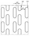
이중 패터닝 기술은 노광 과정의 해상력 한계를 극복할 수 있는 방법으로 평가되고 있지만, 1차 패터닝 과정과 2차 패터닝 과정 간에 중첩 오정렬(overlay misalign)이 유발되는 위험이 있다. 이중 패터닝에 의해 형성된 미세 패턴들의 레이아웃(layout)을 보여주는 도 1을 참조하면, 1차 패턴(10)과 2차 패턴(20) 사이에 오정렬이 유발될 경우, 1차 패턴과 2차 패턴들 사이의 간격이 달라질 수 있다. 즉, 제1간격(d1)과 제2간격(d2)이 동일한 값으로 유지되어야 하지만, 오정렬에 의해 달라져 제2간격(d2)이 상대적으로 좁아지는 불량이 유발될 수 있다. 이와 같이 좁아진 제2간격(d2)을 절연층이 채워 격리시킬 때, 절연층의 갭 채움(gap filling) 불량이 유발될 수 있다.Although double patterning technology is being evaluated as a way to overcome the resolution limitation of the exposure process, there is a risk of causing an overlay misalignment between the first patterning process and the second patterning process. Referring to FIG. 1, which shows the layout of the fine patterns formed by the double patterning, when misalignment is caused between the
본 발명은 1차 패턴과 2차 패턴의 오정렬을 억제할 수 있는 이중 패터닝(double patterning)을 이용한 미세 패턴 형성 방법을 제시하고자 한다.The present invention is to propose a method of forming a fine pattern using double patterning that can suppress misalignment of the primary pattern and the secondary pattern.
본 발명의 일 관점은, 반도체 기판 상에 패터닝(patterning) 대상층을 형성하는 단계; 상기 패터닝 대상층 상에 1차 마스크 패턴들을 형성하는 단계; 상기 1차 마스크 패턴들을 덮는 스페이서층(spacer layer)을 형성하는 단계; 상기 스페이서층 상에 2차 마스크층을 형성하는 단계; 상기 2차 마스크층을 리세스(recess)하여 1차 분리된 2차 마스크 제1패턴을 형성하는 단계; 상기 스페이서층이 노출되게 상기 2차 마스크 제1패턴의 일부를 선택적 식각하여 2차 마스크 제2패턴들로 2차 분리시키는 단계; 상기 2차 마스크 제2패턴들에 노출된 상기 스페이서층 부분을 선택적으로 제거하는 단계; 및 상기 1차 마스크 패턴 및 상기 2차 마스크 제2패턴들을 식각 마스크로 상기 패터닝 대상층을 선택적으로 식각하는 단계를 포함하는 이중 패터닝을 이용한 미세 패턴 형성 방법을 제시한다.One aspect of the invention, forming a patterning target layer on a semiconductor substrate; Forming primary mask patterns on the patterning target layer; Forming a spacer layer covering the primary mask patterns; Forming a second mask layer on the spacer layer; Recessing the secondary mask layer to form a primary mask first pattern separated from each other; Selectively etching a portion of the second mask first pattern to expose the spacer layer to second separation of the second mask second patterns; Selectively removing portions of the spacer layer exposed to the second mask second patterns; And selectively etching the patterning target layer using the first mask pattern and the second mask second patterns as an etch mask.
본 발명의 다른 일 관점은, 1차 목표 패턴들의 배열 및 2차 목표 패턴들의 배열이 교번적으로 배치된 미세 패턴 레이아웃을 얻는 단계; 반도체 기판 상에 상기 패턴 레이아웃이 전사될 패터닝(patterning) 대상층을 형성하는 단계; 상기 패터닝 대상층 상에 상기 1차 목표 패턴들의 레이아웃이 전사된 1차 마스크 패턴들을 형성하는 단계; 상기 1차 마스크 패턴들을 덮는 스페이서층(spacer layer)을 형성 하는 단계; 상기 스페이서층 상에 2차 마스크층을 형성하는 단계; 상기 2차 마스크층을 리세스(recess)하여 상기 스페이서층에 의해 분리된 2차 마스크 제1패턴들을 형성하는 단계; 상기 스페이서층이 노출되게 상기 2차 마스크 제1패턴을 선택적 식각하여 상기 2차 목표 패턴 레이아웃을 따르는 2차 마스크 제2패턴을 형성하는 단계; 상기 2차 마스크 제2패턴에 노출된 상기 스페이서층 부분을 선택적으로 제거하여 상기 패터닝 대상층 부분을 노출시키는 단계; 및 상기 1차 마스크 패턴 및 상기 2차 마스크 제2패턴에 의해 노출된 상기 패터닝 대상층 부분을 선택적으로 식각하여 미세 패턴들을 형성하는 단계를 포함하는 이중 패터닝을 이용한 미세 패턴 형성 방법을 제시한다.According to another aspect of the present invention, there is provided a method including: obtaining a fine pattern layout in which an arrangement of primary target patterns and an arrangement of secondary target patterns are alternately arranged; Forming a patterning target layer on which a pattern layout is to be transferred; Forming primary mask patterns on which the layout of the primary target patterns is transferred on the patterning target layer; Forming a spacer layer covering the primary mask patterns; Forming a second mask layer on the spacer layer; Recessing the secondary mask layer to form secondary mask first patterns separated by the spacer layer; Selectively etching the second mask first pattern to expose the spacer layer to form a second mask second pattern that conforms to the second target pattern layout; Selectively removing the spacer layer portion exposed to the second mask second pattern to expose the patterning target layer portion; And selectively etching the portion of the patterning target layer exposed by the first mask pattern and the second mask second pattern to form fine patterns.
상기 스페이서층 간 사이의 폭이 상기 2차 목표 패턴의 폭에 대등하게 유지되게 증착될 수 있다.The width between the spacer layers may be deposited to be equal to the width of the secondary target pattern.
상기 스페이서층을 리세스하는 단계는 상기 스페이서층을 화학기계적연마(CMP) 또는 에치백(etch back)하여 상기 1차 마스크 패턴의 상측을 덮는 상기 스페이서층 부분의 표면을 노출시켜 상기 스페이서층에 의해 상기 2차 마스크 제1패턴들이 분리되게 수행될 수 있다.Recessing the spacer layer may be performed by chemical mechanical polishing (CMP) or etch back of the spacer layer to expose a surface of the portion of the spacer layer covering the upper side of the primary mask pattern by the spacer layer. The secondary mask first patterns may be separated.
상기 2차 마스크 제2패턴을 형성하는 단계는 상기 2차 마스크 제1패턴 상에 상기 2차 목표 패턴들의 레이아웃을 따르는 포토레지스트 패턴을 형성하는 단계; 및 상기 포토레지스트 패턴 및 상기 스페이서층을 식각 마스크로 상기 2차 마스크 제1패턴을 선택적으로 식각하는 단계를 포함할 수 있다.The forming of the second mask second pattern may include forming a photoresist pattern on the second mask first pattern that follows a layout of the second target patterns; And selectively etching the second mask first pattern using the photoresist pattern and the spacer layer as an etching mask.
상기 미세 패턴들을 식각 마스크로 하부에 노출되는 상기 반도체 기판 부분 을 선택적으로 식각하여 트렌치(trench)를 형성하는 단계; 및 상기 트렌치를 채우는 절연층을 형성하는 단계를 더 수행할 수 있다.Selectively etching the portion of the semiconductor substrate exposed under the micro patterns using an etching mask to form a trench; And forming an insulating layer filling the trench.
본 발명의 실시예는, 1차 패턴을 형성한 후 간격을 균일하게 확보하는 스페이서층(spacer layer)을 도입하고, 스페이서층 상에 2차 패턴을 형성함으로써, 1차 패턴과 2차 패턴 간의 오정렬이 발생되어도 1차 패턴과 2차 패턴 사이의 간격이 유지되도록 하는 미세 패턴 형성 방법을 제시할 수 있다.Embodiments of the present invention provide a misalignment between a primary pattern and a secondary pattern by introducing a spacer layer that uniformly secures the gap after forming the primary pattern and forming a secondary pattern on the spacer layer. Even if this occurs, it is possible to provide a method for forming a fine pattern such that the gap between the primary pattern and the secondary pattern is maintained.
본 발명의 실시예는 디램(DRAM) 소자와 같은 반도체 소자의 활성 영역(active region)을 설정하는 소자분리 영역을 형성하는 소자분리 과정에 이용되는 마스크 패턴(mask pattern)의 배열을 이중 패터닝 기술을 이용한 미세 패턴 형성 방법으로 형성할 수 있다. 이때, 마스크 패턴을 위한 층 상에 1차 패턴을 형성한 후 1차 패턴과 후속의 2차 패턴 사이의 간격을 일정한 간격으로 확보하는 스페이서층(spacer layer)을 도입한다. 이후에, 스페이서층 상에 2차 패턴을 형성함으로써, 1차 패턴의 측벽 상에 위치하는 스페이서층의 폭만큼으로 1차 패턴과 2차 패턴의 사이의 간격을 확보할 수 있다. 2차 패턴이 1차 패턴과 중첩 정렬되는 정도가 설정된 기준에서 벗어나 오정렬되어도, 1차 패턴의 측벽 상에 위치하는 스페이서층 부분이 오정렬에 의해 사이 간격이 축소되는 것을 막아주는 역할을 한다.In an embodiment of the present invention, a double patterning technique uses an array of mask patterns used in a device isolation process to form a device isolation region that sets an active region of a semiconductor device, such as a DRAM device. It can form by the used fine pattern formation method. In this case, after forming a primary pattern on the layer for the mask pattern, a spacer layer is introduced to secure a gap between the primary pattern and the subsequent secondary pattern at a constant interval. Thereafter, by forming the secondary pattern on the spacer layer, the gap between the primary pattern and the secondary pattern can be secured by the width of the spacer layer located on the sidewall of the primary pattern. Even if the degree to which the secondary pattern overlaps with the primary pattern is misaligned outside the set standard, the spacer layer positioned on the sidewall of the primary pattern serves to prevent the gap between the secondary patterns from being reduced by misalignment.
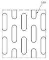
도 2 내지 도 15는 본 발명의 실시예에 따른 이중 패터닝을 이용한 미세 패턴 형성 방법을 보여준다.2 to 15 show a method of forming a fine pattern using double patterning according to an embodiment of the present invention.
도 2를 참조하면, 반도체 기판 상에 형성하고자하는 목표(target) 패턴(100)들이 배열된 레이아웃을 설계한다. 이때, 미세 크기의 목표 패턴(100)은 디램(DRAM) 소자의 소자분리(isolation) 형성 과정에서 사용될 마스크 패턴으로 설정될 수 있다. 이러한 마스크 패턴은 반도체 기판의 활성 영역(active region)의 레이아웃으로 설정되며, 소자분리 영역이 위치할 부분, 즉, 소자분리 절연층으로 채워질 트렌치(trench)가 형성될 영역을 여는 패턴으로 설계된다.Referring to FIG. 2, a layout in which
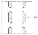
도 3을 참조하면, 목표 패턴(100)의 레이아웃으로부터 1차 패터닝 과정에서 형성될 1차 목표 패턴(101)의 레이아웃과 2차 패터닝 과정에서 형성될 2차 목표 패턴(103)들의 레이아웃으로 분리한다. 이때, 1차 목표 패턴(101)은 짝수 열의 패턴들로, 2차 목표 패턴(103)은 홀수 열의 패턴들로 분리할 수 있다.Referring to FIG. 3, the layout of the
도 4를 참조하면, 반도체 기판(210) 상에 패터닝 대상층(220)을 형성하고, 설계된 1차 목표 패턴(도 3의 101)의 레이아웃을 따르는 1차 마스크 패턴(231)을 1차 패터닝한다. 패터닝 대상층(220)은 반도체 기판(210)에 소자분리용 트렌치를 선택적 식각할 때 하드 마스크(hard mask)로 이용될 실리콘 산화물 및 질화물의 패드층(pad layer)으로 형성될 수 있다. 1차 마스크 패턴(231)을 위한 층, 예컨대 실리콘산화물(SiO2)층을 패터닝 대상층(220) 상에 형성하고, 1차 마스크 패턴(231)을 위한 1차 마스크층 상에 제1포토레지스트층을 형성하고, 제1포토레지스트층에 설계된 1차 목표 패턴(도 3의 101)의 레이아웃을 1차 노광 및 현상으로 패턴 전사하여 제1포토레지스트 패턴(241)을 형성한다. 제1포토레지스트 패턴(241)에 식각 마스크로 1차 마스크 패턴(231)을 위한 층을 선택적 식각하여 1차 마스크 패턴(231)을 형성한다. 형성된 1차 마스크 패턴(231)의 평면 레이아웃은 도 5에 제시된 바와 같이 설계된 1차 목표 패턴(도 3의 101)의 레이아웃을 따른다. 따라서, 1차 목표 패턴(도 3의 101) 간의 제3간격 d3은 2차 목표 패턴(도 3의 103)이 형성될 위치를 포함하여 넓은 간격을 가진다.Referring to FIG. 4, the
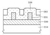
도 6을 참조하면, 1차 마스크 패턴(231) 상에 스페이서층(250)을 형성한다. 스페이서층(250)은 1차 마스크 패턴(231)과 식각 선택비를 가지는 절연 물질, 예컨대, 실리콘질화물(Si3N4)을 포함하여 형성될 수 있다. 스페이서층(250)은 1차 목표 패턴(도 3의 101)과 후속의 2차 목표 패턴(도 3의 103) 사이의 간격을 일정한 간격으로 확보하게 도입되며, 서로 마주보는 1차 마스크 패턴(231)들의 측벽 상에 위치하는 스페이서층(250) 부분들 사이의 제4간격 d4가 2차 목표 패턴(103)의 선폭과 대등한 폭을 가지게 스페이서층(250)의 두께가 설정된다.Referring to FIG. 6, a
도 7을 참조하면, 스페이서층(250) 상에 사이 제4간격 d4 부분을 채우는 2차 목표 패턴(도 3의 103)을 위한 2차 마스크층(260)을 증착한다. 2차 마스크층(260)은 스페이서층(250)과 식각 선택비를 가지는 절연 물질, 예컨대, 실리콘산화물의 층으로 형성될 수 있다.Referring to FIG. 7, a
도 8을 참조하면, 2차 마스크층(260)을 화학기계적연마(CMP)와 같은 평탄화 방법으로 평탄화하거나 에치백(etch back)하여 1차 마스크 패턴(231) 상측을 덮는 스페이서층(250) 부분의 표면이 노출되게 한다. CMP 또는 에치백으로 2차 마스크 층(260)이 리세스(recess)되어 스페이서층(250) 사이의 제4간격 d4 부분을 채우는 2차 마스크층 제1패턴(261)으로 패터닝된다. 이와 같은 2차 마스크층 제1패턴(261)은 도 9의 평면도에 제시된 바와 같이 라인(line) 형상을 가지게 패터닝된다.Referring to FIG. 8, a portion of the
도 10 및 도 11을 참조하면, 2차 마스크층 제1패턴(261) 상에 2차 목표 패턴(도 3의 103)의 형상을 따르는 제2포토레지스트 패턴(270)을 형성한다. 제2포토레지스트 패턴(270)은 제2포토레지스트층을 도포하고, 설계된 2차 목표 패턴(도 3의 103)의 레이아웃을 2차 노광 및 현상으로 패턴 전사하여 형성된다. 이때, 2차 노광 과정은 1차 노광 과정과 패턴 정렬을 수행하지만, 어느 정도의 오정렬이 유발될 수 있다. 따라서, 제2포토레지스트 패턴(270)과 하부의 1차 마스크 패턴(231) 사이에 오정렬에 따른 위치 변동(shift)이 유발될 수 있다.10 and 11, a second
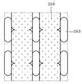
도 12를 도 11과 함께 참조하면, 제2포토레지스트 패턴(270)에 의해 노출된 2차 마스크층 제1패턴(261) 부분을 선택적으로 식각하여 2차 마스크층 제2패턴, 즉, 2차 마스크 패턴(263)들로 분리시킨다. 이러한 선택적 식각 과정에서 스페이서층(250)은 식각 장벽으로 작용하여 2차 마스크 패턴(263)과 1차 마스크 패턴(231) 간의 간격이 스페이서층(250)의 폭만큼 유지되게 확보한다.Referring to FIG. 12 together with FIG. 11, a portion of the second mask layer
도 13 및 도 14를 참조하면, 2차 마스크 패턴(263)을 식각 마스크로 이용하여 노출된 스페이서층(250) 부분을 선택적으로 식각한다. 이때, 스페이서층(250)의 식각에 의해 노출되는 1차 마스크 패턴(231)은 식각 장벽으로 작용하여 그 패턴 형상이 유지된다. 따라서, 1차 마스크 패턴(231)과 2차 마스크 패턴(263) 사이의 스페이서층(250) 부분이 선택적 식각으로 제거되고, 2차 마스크 패턴(263)에 정렬되 는 스페이서층(250) 부분이 스페이서층 패턴(253)으로 잔류한다. 이와 같이 스페이서층(250)의 선택적 제거에 의해, 패터닝 대상층(220) 상에 1차 마스크 패턴(231) 및 2차 마스크 패턴(263)이 미세 패턴(도 2의 100)으로 형성된다. 이러한 1차 마스크 패턴(231)과 2차 마스크 패턴(263)은 각각 분리된 2차례의 노광 및 식각 과정의 패터닝 과정으로 각각 형성되지만, 스페이서층(250)의 폭에 의해 1차 마스크 패턴(231)과 2차 마스크 패턴(263) 사이의 간격이 일정하게 유지되게 된다.13 and 14, the exposed portion of the
도 14 및 도 15를 참조하면, 1차 마스크 패턴(231) 및 2차 마스크 패턴(263)을 식각 마스크로 노출된 패터닝 대상층(220) 부분을 선택적으로 식각하여 미세 패턴(225)을 형성한다. 이후에, 미세 패턴(225)에 의해 노출된 반도체 기판(210) 부분을 선택적으로 식각하여 활성 영역을 설정하는 소자분리용 트렌치(211)를 형성한다. 이후에, 소자분리용 트렌치(211)를 채우는 소자분리용 절연층(231)을 형성하여 소자분리 구조를 구현한다. 1차 마스크 패턴(231)과 2차 마스크 패턴(263)이 스페이서층(250)에 의해 일정 간격을 가지게 유지되므로, 트렌치(211)들의 선폭은 상호 간에 균일한 크기로 형성될 수 있다. 따라서, 도 1의 1차 패턴(10)과 2차 패턴(20) 간의 오정렬에 의해 트렌치의 선폭이 원하지 않게 좁아져, 트렌치를 채우는 절연층의 채움 특성이 열화되는 것을 억제할 수 있다.14 and 15, the
본 발명의 실시예에서는 이중 패터닝 기술을 적용할 때, 중첩 오정렬이 발생하더라도 1차 패턴과 2차 패턴의 간격을 일정하게 유지할 수 있다. 따라서, 이중 패터닝 기술을 소자분리용의 트렌치를 형성하는 데 적용하여, 보다 미세한 크기의 소자분리 구조를 구현할 수 있다.In the embodiment of the present invention, even when overlapping misalignment occurs when the double patterning technique is applied, the interval between the primary pattern and the secondary pattern may be kept constant. Therefore, by applying a double patterning technique to form a trench for device isolation, it is possible to implement a finer device isolation structure.
도 1은 종래의 이중 패터닝 기술에서의 패턴 오정렬(misalignment)을 보여주는 평면도이다.1 is a plan view showing pattern misalignment in a conventional double patterning technique.
도 2 내지 도 15는 본 발명의 실시예에 따른 이중 패터닝을 이용한 미세 패턴 형성 방법을 설명하기 위해 제시한 도면들이다.2 to 15 are diagrams provided to explain a method for forming a fine pattern using double patterning according to an embodiment of the present invention.
Claims (6)
Translated fromKoreanPriority Applications (1)
| Application Number | Priority Date | Filing Date | Title |
|---|---|---|---|
| KR1020080131678AKR101045371B1 (en) | 2008-12-22 | 2008-12-22 | Micro pattern formation method using double patterning |
Applications Claiming Priority (1)
| Application Number | Priority Date | Filing Date | Title |
|---|---|---|---|
| KR1020080131678AKR101045371B1 (en) | 2008-12-22 | 2008-12-22 | Micro pattern formation method using double patterning |
Publications (2)
| Publication Number | Publication Date |
|---|---|
| KR20100073092A KR20100073092A (en) | 2010-07-01 |
| KR101045371B1true KR101045371B1 (en) | 2011-06-30 |
Family
ID=42636118
Family Applications (1)
| Application Number | Title | Priority Date | Filing Date |
|---|---|---|---|
| KR1020080131678AExpired - Fee RelatedKR101045371B1 (en) | 2008-12-22 | 2008-12-22 | Micro pattern formation method using double patterning |
Country Status (1)
| Country | Link |
|---|---|
| KR (1) | KR101045371B1 (en) |
Families Citing this family (1)
| Publication number | Priority date | Publication date | Assignee | Title |
|---|---|---|---|---|
| KR102274738B1 (en) | 2016-01-08 | 2021-07-07 | 삼성전자주식회사 | Semiconductor device and method for fabricating the same |
Citations (4)
| Publication number | Priority date | Publication date | Assignee | Title |
|---|---|---|---|---|
| KR20060134330A (en)* | 2005-06-22 | 2006-12-28 | 주식회사 하이닉스반도체 | Micro pattern formation method using double exposure process |
| KR20070002861A (en)* | 2005-06-30 | 2007-01-05 | 삼성전자주식회사 | Method of forming fine pattern of semiconductor device |
| KR100843241B1 (en) | 2007-03-29 | 2008-07-02 | 삼성전자주식회사 | Manufacturing method of semiconductor device |
| KR20080107557A (en)* | 2007-06-07 | 2008-12-11 | 삼성전자주식회사 | Method of forming a fine pattern employing self-aligned double patterning |
- 2008
- 2008-12-22KRKR1020080131678Apatent/KR101045371B1/ennot_activeExpired - Fee Related
Patent Citations (4)
| Publication number | Priority date | Publication date | Assignee | Title |
|---|---|---|---|---|
| KR20060134330A (en)* | 2005-06-22 | 2006-12-28 | 주식회사 하이닉스반도체 | Micro pattern formation method using double exposure process |
| KR20070002861A (en)* | 2005-06-30 | 2007-01-05 | 삼성전자주식회사 | Method of forming fine pattern of semiconductor device |
| KR100843241B1 (en) | 2007-03-29 | 2008-07-02 | 삼성전자주식회사 | Manufacturing method of semiconductor device |
| KR20080107557A (en)* | 2007-06-07 | 2008-12-11 | 삼성전자주식회사 | Method of forming a fine pattern employing self-aligned double patterning |
Also Published As
| Publication number | Publication date |
|---|---|
| KR20100073092A (en) | 2010-07-01 |
Similar Documents
| Publication | Publication Date | Title |
|---|---|---|
| KR101087835B1 (en) | Method of forming fine pattern of semiconductor device | |
| US7700456B2 (en) | Semiconductor device and manufacturing method of the same | |
| JP5606388B2 (en) | Pattern formation method | |
| US9269606B2 (en) | Spacer enabled active isolation for an integrated circuit device | |
| CN101140417B (en) | Semiconductor device with a bulb-type recess gate | |
| US10276395B2 (en) | Method for manufacturing semiconductor device | |
| JP2001176959A (en) | Semiconductor device and method of manufacturing the same | |
| CN110957209B (en) | Multiple patterning method and memory forming method | |
| US20090096116A1 (en) | Alignment mark and mehtod for forming the same | |
| US20070048938A1 (en) | Method of manufacturing MOS transistor with multiple channel structure | |
| KR100739656B1 (en) | Manufacturing Method of Semiconductor Device | |
| JP5690489B2 (en) | Method for forming semiconductor device | |
| KR100568452B1 (en) | A method of manufacturing a semiconductor device having an alignment key and a semiconductor device manufactured thereby. | |
| KR101045371B1 (en) | Micro pattern formation method using double patterning | |
| US20100227451A1 (en) | Method for manufacturing semiconductor device | |
| KR20160005945A (en) | Mask pattern and method for forming fine patterns of a semiconductor device | |
| JP5114844B2 (en) | Manufacturing method of semiconductor device | |
| TWI495089B (en) | Semiconductor memory array structure | |
| JP2009094379A (en) | Manufacturing method of semiconductor device | |
| KR20140028906A (en) | Semiconductor device and method for manufacturing the same | |
| KR100995142B1 (en) | Contact hole formation method of semiconductor device | |
| KR20090054235A (en) | Method for forming damascene pattern using self-aligned double patterning method and method for extracting photomask layout | |
| JP2009065151A (en) | Semiconductor device and its manufacturing method | |
| JP4786697B2 (en) | Semiconductor device | |
| KR101172310B1 (en) | Method for fabricating semiconductor device |
Legal Events
| Date | Code | Title | Description |
|---|---|---|---|
| A201 | Request for examination | ||
| PA0109 | Patent application | St.27 status event code:A-0-1-A10-A12-nap-PA0109 | |
| PA0201 | Request for examination | St.27 status event code:A-1-2-D10-D11-exm-PA0201 | |
| PG1501 | Laying open of application | St.27 status event code:A-1-1-Q10-Q12-nap-PG1501 | |
| E902 | Notification of reason for refusal | ||
| PE0902 | Notice of grounds for rejection | St.27 status event code:A-1-2-D10-D21-exm-PE0902 | |
| E13-X000 | Pre-grant limitation requested | St.27 status event code:A-2-3-E10-E13-lim-X000 | |
| P11-X000 | Amendment of application requested | St.27 status event code:A-2-2-P10-P11-nap-X000 | |
| P13-X000 | Application amended | St.27 status event code:A-2-2-P10-P13-nap-X000 | |
| E701 | Decision to grant or registration of patent right | ||
| PE0701 | Decision of registration | St.27 status event code:A-1-2-D10-D22-exm-PE0701 | |
| GRNT | Written decision to grant | ||
| PR0701 | Registration of establishment | St.27 status event code:A-2-4-F10-F11-exm-PR0701 | |
| PR1002 | Payment of registration fee | St.27 status event code:A-2-2-U10-U11-oth-PR1002 Fee payment year number:1 | |
| PG1601 | Publication of registration | St.27 status event code:A-4-4-Q10-Q13-nap-PG1601 | |
| PN2301 | Change of applicant | St.27 status event code:A-5-5-R10-R13-asn-PN2301 St.27 status event code:A-5-5-R10-R11-asn-PN2301 | |
| PN2301 | Change of applicant | St.27 status event code:A-5-5-R10-R13-asn-PN2301 St.27 status event code:A-5-5-R10-R11-asn-PN2301 | |
| LAPS | Lapse due to unpaid annual fee | ||
| PC1903 | Unpaid annual fee | St.27 status event code:A-4-4-U10-U13-oth-PC1903 Not in force date:20140624 Payment event data comment text:Termination Category : DEFAULT_OF_REGISTRATION_FEE | |
| PN2301 | Change of applicant | St.27 status event code:A-5-5-R10-R13-asn-PN2301 St.27 status event code:A-5-5-R10-R11-asn-PN2301 | |
| PC1903 | Unpaid annual fee | St.27 status event code:N-4-6-H10-H13-oth-PC1903 Ip right cessation event data comment text:Termination Category : DEFAULT_OF_REGISTRATION_FEE Not in force date:20140624 | |
| P22-X000 | Classification modified | St.27 status event code:A-4-4-P10-P22-nap-X000 |