KR101036605B1 - Substrate support unit and sheet type substrate polishing apparatus using the same - Google Patents
Substrate support unit and sheet type substrate polishing apparatus using the sameDownload PDFInfo
- Publication number
- KR101036605B1 KR101036605B1KR1020080062444AKR20080062444AKR101036605B1KR 101036605 B1KR101036605 B1KR 101036605B1KR 1020080062444 AKR1020080062444 AKR 1020080062444AKR 20080062444 AKR20080062444 AKR 20080062444AKR 101036605 B1KR101036605 B1KR 101036605B1
- Authority
- KR
- South Korea
- Prior art keywords
- substrate
- support
- plate
- vacuum plate
- polishing
- Prior art date
- Legal status (The legal status is an assumption and is not a legal conclusion. Google has not performed a legal analysis and makes no representation as to the accuracy of the status listed.)
- Active
Links
- 239000000758substrateSubstances0.000titleclaimsabstractdescription255
- 238000005498polishingMethods0.000titleclaimsabstractdescription119
- 238000004140cleaningMethods0.000claimsabstractdescription98
- 238000000034methodMethods0.000claimsabstractdescription50
- 238000007517polishing processMethods0.000claimsabstractdescription31
- 239000007788liquidSubstances0.000claimsdescription39
- 238000003825pressingMethods0.000claimsdescription14
- 239000013013elastic materialSubstances0.000claimsdescription3
- 230000003028elevating effectEffects0.000claimsdescription2
- 230000003139buffering effectEffects0.000claims1
- 230000002265preventionEffects0.000claims1
- 238000011084recoveryMethods0.000description24
- 230000003750conditioning effectEffects0.000description13
- 239000008367deionised waterSubstances0.000description13
- 229910021641deionized waterInorganic materials0.000description13
- XLYOFNOQVPJJNP-UHFFFAOYSA-NwaterChemical compoundOXLYOFNOQVPJJNP-UHFFFAOYSA-N0.000description13
- 239000000126substanceSubstances0.000description8
- 229910003460diamondInorganic materials0.000description6
- 239000010432diamondSubstances0.000description6
- 239000004065semiconductorSubstances0.000description4
- 239000000463materialSubstances0.000description3
- 229910052751metalInorganic materials0.000description3
- 239000002184metalSubstances0.000description3
- 238000000926separation methodMethods0.000description3
- 230000035939shockEffects0.000description3
- 238000005406washingMethods0.000description3
- 238000004519manufacturing processMethods0.000description2
- 238000010297mechanical methods and processMethods0.000description2
- 238000001179sorption measurementMethods0.000description2
- 230000003746surface roughnessEffects0.000description2
- YCKRFDGAMUMZLT-UHFFFAOYSA-NFluorine atomChemical compound[F]YCKRFDGAMUMZLT-UHFFFAOYSA-N0.000description1
- 238000005452bendingMethods0.000description1
- 230000000593degrading effectEffects0.000description1
- 238000005137deposition processMethods0.000description1
- 238000005530etchingMethods0.000description1
- 229910052731fluorineInorganic materials0.000description1
- 239000011737fluorineSubstances0.000description1
- 230000001771impaired effectEffects0.000description1
- 238000012986modificationMethods0.000description1
- 230000004048modificationEffects0.000description1
- 230000003287optical effectEffects0.000description1
- 239000002245particleSubstances0.000description1
- 230000000149penetrating effectEffects0.000description1
- 238000000206photolithographyMethods0.000description1
- 229920001296polysiloxanePolymers0.000description1
- 210000000582semenAnatomy0.000description1
- 239000010409thin filmSubstances0.000description1
- WFKWXMTUELFFGS-UHFFFAOYSA-NtungstenChemical compound[W]WFKWXMTUELFFGS-UHFFFAOYSA-N0.000description1
- 229910052721tungstenInorganic materials0.000description1
- 239000010937tungstenSubstances0.000description1
- 238000004148unit processMethods0.000description1
Images


Classifications
- H—ELECTRICITY
- H01—ELECTRIC ELEMENTS
- H01L—SEMICONDUCTOR DEVICES NOT COVERED BY CLASS H10
- H01L21/00—Processes or apparatus adapted for the manufacture or treatment of semiconductor or solid state devices or of parts thereof
- H01L21/02—Manufacture or treatment of semiconductor devices or of parts thereof
- H01L21/04—Manufacture or treatment of semiconductor devices or of parts thereof the devices having potential barriers, e.g. a PN junction, depletion layer or carrier concentration layer
- H01L21/18—Manufacture or treatment of semiconductor devices or of parts thereof the devices having potential barriers, e.g. a PN junction, depletion layer or carrier concentration layer the devices having semiconductor bodies comprising elements of Group IV of the Periodic Table or AIIIBV compounds with or without impurities, e.g. doping materials
- H01L21/30—Treatment of semiconductor bodies using processes or apparatus not provided for in groups H01L21/20 - H01L21/26
- H01L21/302—Treatment of semiconductor bodies using processes or apparatus not provided for in groups H01L21/20 - H01L21/26 to change their surface-physical characteristics or shape, e.g. etching, polishing, cutting
- H01L21/304—Mechanical treatment, e.g. grinding, polishing, cutting
- B—PERFORMING OPERATIONS; TRANSPORTING
- B24—GRINDING; POLISHING
- B24B—MACHINES, DEVICES, OR PROCESSES FOR GRINDING OR POLISHING; DRESSING OR CONDITIONING OF ABRADING SURFACES; FEEDING OF GRINDING, POLISHING, OR LAPPING AGENTS
- B24B37/00—Lapping machines or devices; Accessories
- B24B37/27—Work carriers
- B24B37/30—Work carriers for single side lapping of plane surfaces
- H—ELECTRICITY
- H01—ELECTRIC ELEMENTS
- H01L—SEMICONDUCTOR DEVICES NOT COVERED BY CLASS H10
- H01L21/00—Processes or apparatus adapted for the manufacture or treatment of semiconductor or solid state devices or of parts thereof
- H01L21/67—Apparatus specially adapted for handling semiconductor or electric solid state devices during manufacture or treatment thereof; Apparatus specially adapted for handling wafers during manufacture or treatment of semiconductor or electric solid state devices or components ; Apparatus not specifically provided for elsewhere
- H01L21/68—Apparatus specially adapted for handling semiconductor or electric solid state devices during manufacture or treatment thereof; Apparatus specially adapted for handling wafers during manufacture or treatment of semiconductor or electric solid state devices or components ; Apparatus not specifically provided for elsewhere for positioning, orientation or alignment
- H—ELECTRICITY
- H01—ELECTRIC ELEMENTS
- H01L—SEMICONDUCTOR DEVICES NOT COVERED BY CLASS H10
- H01L21/00—Processes or apparatus adapted for the manufacture or treatment of semiconductor or solid state devices or of parts thereof
- H01L21/67—Apparatus specially adapted for handling semiconductor or electric solid state devices during manufacture or treatment thereof; Apparatus specially adapted for handling wafers during manufacture or treatment of semiconductor or electric solid state devices or components ; Apparatus not specifically provided for elsewhere
- H01L21/683—Apparatus specially adapted for handling semiconductor or electric solid state devices during manufacture or treatment thereof; Apparatus specially adapted for handling wafers during manufacture or treatment of semiconductor or electric solid state devices or components ; Apparatus not specifically provided for elsewhere for supporting or gripping
- H01L21/6838—Apparatus specially adapted for handling semiconductor or electric solid state devices during manufacture or treatment thereof; Apparatus specially adapted for handling wafers during manufacture or treatment of semiconductor or electric solid state devices or components ; Apparatus not specifically provided for elsewhere for supporting or gripping with gripping and holding devices using a vacuum; Bernoulli devices
- H—ELECTRICITY
- H01—ELECTRIC ELEMENTS
- H01L—SEMICONDUCTOR DEVICES NOT COVERED BY CLASS H10
- H01L21/00—Processes or apparatus adapted for the manufacture or treatment of semiconductor or solid state devices or of parts thereof
- H01L21/67—Apparatus specially adapted for handling semiconductor or electric solid state devices during manufacture or treatment thereof; Apparatus specially adapted for handling wafers during manufacture or treatment of semiconductor or electric solid state devices or components ; Apparatus not specifically provided for elsewhere
- H01L21/683—Apparatus specially adapted for handling semiconductor or electric solid state devices during manufacture or treatment thereof; Apparatus specially adapted for handling wafers during manufacture or treatment of semiconductor or electric solid state devices or components ; Apparatus not specifically provided for elsewhere for supporting or gripping
- H01L21/687—Apparatus specially adapted for handling semiconductor or electric solid state devices during manufacture or treatment thereof; Apparatus specially adapted for handling wafers during manufacture or treatment of semiconductor or electric solid state devices or components ; Apparatus not specifically provided for elsewhere for supporting or gripping using mechanical means, e.g. chucks, clamps or pinches
- H01L21/68714—Apparatus specially adapted for handling semiconductor or electric solid state devices during manufacture or treatment thereof; Apparatus specially adapted for handling wafers during manufacture or treatment of semiconductor or electric solid state devices or components ; Apparatus not specifically provided for elsewhere for supporting or gripping using mechanical means, e.g. chucks, clamps or pinches the wafers being placed on a susceptor, stage or support
- H01L21/68728—Apparatus specially adapted for handling semiconductor or electric solid state devices during manufacture or treatment thereof; Apparatus specially adapted for handling wafers during manufacture or treatment of semiconductor or electric solid state devices or components ; Apparatus not specifically provided for elsewhere for supporting or gripping using mechanical means, e.g. chucks, clamps or pinches the wafers being placed on a susceptor, stage or support characterised by a plurality of separate clamping members, e.g. clamping fingers
- H—ELECTRICITY
- H01—ELECTRIC ELEMENTS
- H01L—SEMICONDUCTOR DEVICES NOT COVERED BY CLASS H10
- H01L21/00—Processes or apparatus adapted for the manufacture or treatment of semiconductor or solid state devices or of parts thereof
- H01L21/67—Apparatus specially adapted for handling semiconductor or electric solid state devices during manufacture or treatment thereof; Apparatus specially adapted for handling wafers during manufacture or treatment of semiconductor or electric solid state devices or components ; Apparatus not specifically provided for elsewhere
- H01L21/683—Apparatus specially adapted for handling semiconductor or electric solid state devices during manufacture or treatment thereof; Apparatus specially adapted for handling wafers during manufacture or treatment of semiconductor or electric solid state devices or components ; Apparatus not specifically provided for elsewhere for supporting or gripping
- H01L21/687—Apparatus specially adapted for handling semiconductor or electric solid state devices during manufacture or treatment thereof; Apparatus specially adapted for handling wafers during manufacture or treatment of semiconductor or electric solid state devices or components ; Apparatus not specifically provided for elsewhere for supporting or gripping using mechanical means, e.g. chucks, clamps or pinches
- H01L21/68714—Apparatus specially adapted for handling semiconductor or electric solid state devices during manufacture or treatment thereof; Apparatus specially adapted for handling wafers during manufacture or treatment of semiconductor or electric solid state devices or components ; Apparatus not specifically provided for elsewhere for supporting or gripping using mechanical means, e.g. chucks, clamps or pinches the wafers being placed on a susceptor, stage or support
- H01L21/68742—Apparatus specially adapted for handling semiconductor or electric solid state devices during manufacture or treatment thereof; Apparatus specially adapted for handling wafers during manufacture or treatment of semiconductor or electric solid state devices or components ; Apparatus not specifically provided for elsewhere for supporting or gripping using mechanical means, e.g. chucks, clamps or pinches the wafers being placed on a susceptor, stage or support characterised by a lifting arrangement, e.g. lift pins
Landscapes
- Engineering & Computer Science (AREA)
- Microelectronics & Electronic Packaging (AREA)
- Condensed Matter Physics & Semiconductors (AREA)
- General Physics & Mathematics (AREA)
- Manufacturing & Machinery (AREA)
- Computer Hardware Design (AREA)
- Physics & Mathematics (AREA)
- Power Engineering (AREA)
- Mechanical Engineering (AREA)
- Finish Polishing, Edge Sharpening, And Grinding By Specific Grinding Devices (AREA)
- Mechanical Treatment Of Semiconductor (AREA)
- Container, Conveyance, Adherence, Positioning, Of Wafer (AREA)
- Constituent Portions Of Griding Lathes, Driving, Sensing And Control (AREA)
- Cleaning Or Drying Semiconductors (AREA)
Abstract
Translated fromKorean
Description
Translated fromKorean본 발명은 반도체 제조 장치 및 방법에 관한 것으로서, 보다 상세하게는 반도체 기판을 매엽 처리 방식으로 지지하는 기판 지지 유닛과 이를 이용하여 기판을 연마 및 세정하는 기판 연마 장치에 관한 것이다.BACKGROUND OF THE
일반적으로 반도체 소자의 제조 공정은 박막의 형성 및 적층을 위해 증착 공정, 사진 공정, 식각 공정 등 다수의 단위 공정들을 반복 수행해야만 한다. 웨이퍼 상에 요구되는 소정의 회로 패턴이 형성될 때까지 이들 공정은 반복되며, 회로 패턴이 형성된 후 웨이퍼의 표면에는 많은 굴곡이 생기게 된다. 최근 반도체 소자는 고집적화에 따라 그 구조가 다층화되며, 웨이퍼 표면의 굴곡의 수와 이들 사이의 단차가 증가하고 있다. 웨이퍼 표면의 비평탄화는 사진 공정에서 디포커스(Defocus) 등의 문제를 발생시키므로 웨이퍼의 표면을 평탄화하기 위해 주기적으로 웨이퍼 표면을 연마하여야 한다.In general, a semiconductor device manufacturing process must repeatedly perform a plurality of unit processes such as a deposition process, a photo process, and an etching process to form and stack thin films. These processes are repeated until the desired circuit pattern is formed on the wafer, and after the circuit pattern is formed, a lot of bending occurs on the surface of the wafer. In recent years, as semiconductor devices become highly integrated, their structures are multilayered, and the number of bends on the surface of the wafer and the step between them are increasing. Unplanarization of the wafer surface causes problems such as defocus in the photolithography process, and thus the wafer surface must be polished periodically to planarize the surface of the wafer.
웨이퍼의 표면을 평탄화하기 위해 다양한 표면 평탄화 기술이 있으나 이 중 좁은 영역뿐만 아니라 넓은 영역의 평탄화에 있어서도 우수한 평탄도를 얻을 수 있 는 화학적 기계적 연마(Chemical Mechanical Polishing : CMP) 장치가 주로 사용된다. 화학적 기계적 연마 장치는 텅스텐이나 산화물 등이 입혀진 웨이퍼의 표면을 기계적 마찰에 의해 연마시킴과 동시에 화학적 연마재에 의해 연마시키는 장치로서, 아주 미세한 연마를 가능하게 한다.Various surface planarization techniques are used to planarize the surface of the wafer, but chemical mechanical polishing (CMP) apparatuses, which can obtain excellent flatness not only for narrow areas but also for wide areas, are mainly used. The chemical mechanical polishing apparatus is an apparatus for polishing a surface of a wafer coated with tungsten, an oxide, or the like by mechanical friction and polishing with a chemical abrasive, and enables very fine polishing.
본 발명은 기판의 연마 공정과 후세정 공정을 매엽 방식으로 순차적으로 진행할 수 있는 기판 지지 유닛 및 이를 이용한 매엽식 기판 연마 장치를 제공하기 위한 것이다.An object of the present invention is to provide a substrate support unit capable of sequentially performing a substrate polishing process and a post-cleaning process in a single sheet method, and a single substrate polishing apparatus using the same.
본 발명의 목적은 여기에 제한되지 않으며, 언급되지 않은 또 다른 목적들은 아래의 기재로부터 당업자에게 명확하게 이해될 수 있을 것이다.The objects of the present invention are not limited thereto, and other objects not mentioned can be clearly understood by those skilled in the art from the following description.
상기한 과제를 달성하기 위하여 본 발명에 의한 기판 지지 유닛은 기판을 진공 흡착하는 진공 플레이트; 상기 진공 플레이트의 하부에 이격 배치되며, 상기 기판을 클램핑할 척 부재들이 설치된 지지 플레이트; 및 상기 척 부재들이 상기 진공 플레이트에 놓인 상기 기판을 상기 진공 플레이트로부터 상향 이격된 상태로 지지하도록 상기 진공 플레이트 또는 상기 지지 플레이트를 상하 방향으로 이동시키는 구동 부재를 포함하는 것을 특징으로 한다.In order to achieve the above object, a substrate support unit according to the present invention includes a vacuum plate for vacuum adsorption of a substrate; A support plate disposed below the vacuum plate and provided with chuck members for clamping the substrate; And a driving member for moving the vacuum plate or the support plate in a vertical direction so that the chuck members support the substrate placed on the vacuum plate in a state spaced upwardly from the vacuum plate.
상술한 바와 같은 구성을 가지는 본 발명에 의한 기판 지지 유닛에 있어서, 상기 구동 부재는 상기 지지 플레이트의 아래에 상하 방향을 따라 서로 마주보도록 배치되며, 서로 간에 자기적 반발력이 작용하도록 자극이 배열된 상부 자석 부재 및 하부 자석 부재; 일단이 상기 진공 플레이트에 연결되고 타단이 상기 상부 자석 부재에 연결되는 연결 부재들; 및 상기 하부 자석 부재를 상하 방향으로 이동시키는 직선 구동기를 포함할 수 있다.In the substrate support unit according to the present invention having the configuration as described above, the drive member is disposed to face each other in the up and down direction below the support plate, the magnetic pole is arranged so that the magnetic repulsive force to act on each other A magnet member and a lower magnet member; Connecting members having one end connected to the vacuum plate and the other end connected to the upper magnet member; And it may include a linear driver for moving the lower magnet member in the vertical direction.
상기 상부 자석 부재의 자극들과 상기 하부 자석 부재의 자극들은 환형 구조로 배열될 수 있다.The magnetic poles of the upper magnet member and the magnetic poles of the lower magnet member may be arranged in an annular structure.
상기 연결 부재들은 상기 지지 플레이트에 관통 형성된 홀에 삽입 설치되는 봉 형상일 수 있다.The connection members may have a rod shape inserted into a hole formed through the support plate.
상기 지지 플레이트와 상기 상부 자석 부재 사이에 탄성 반발력이 작용하도록 설치된 탄성 부재를 더 포함할 수 있다.The apparatus may further include an elastic member installed between the support plate and the upper magnet member so that an elastic repulsive force acts.
상기 하부 자석 부재의 기설정된 높이로의 상하 이동 여부를 검출하는 감지 부재를 더 포함할 수 있다.The apparatus may further include a sensing member configured to detect whether the lower magnet member moves up and down to a predetermined height.
상기 척 부재들은 상기 기판의 하면을 지지하는 지지 핀들과 상기 기판의 측면을 지지하는 척킹 핀들을 포함하고, 상기 진공 플레이트에는 상기 진공 플레이트의 상하 이동시 상기 지지 핀들과 상기 척킹 핀들이 삽입되도록 홀들이 관통 형성될 수 있다.The chuck members may include support pins for supporting a lower surface of the substrate and chucking pins for supporting a side surface of the substrate, and holes may pass through the vacuum plate so that the support pins and the chucking pins are inserted when the vacuum plate moves up and down. Can be formed.
진공 흡착된 상기 기판의 이탈을 방지하도록 상기 진공 플레이트의 가장자리에 이탈 방지 턱이 돌출 형성될 수 있다.An anti-separation jaw may protrude from an edge of the vacuum plate to prevent detachment of the vacuum-adsorbed substrate.
진공 흡착된 상기 기판과 상기 진공 플레이트 사이의 이물질에 의해 상기 기판이 변형되는 것을 방지하도록 완충 작용을 하는 탄성 재질의 완충 부재가 상기 진공 플레이트의 상면에 설치될 수 있다.A shock absorbing member made of an elastic material may be installed on the upper surface of the vacuum plate to prevent the substrate from being deformed by the foreign matter between the vacuum adsorbed substrate and the vacuum plate.
상기 구동 부재는 상기 지지 플레이트에 설치된 상부 자석 부재; 상기 상부 자석 부재의 아래에 상기 상부 자석 부재와 마주보도록 배치되며, 상기 상부 자석 부재와의 사이에 자기적 반발력이 작용하도록 자극이 배열된 하부 자석 부재; 및 상기 하부 자석 부재를 상하 방향으로 이동시키는 직선 구동기를 포함할 수 있다.The drive member includes an upper magnet member installed on the support plate; A lower magnet member disposed below the upper magnet member so as to face the upper magnet member, and having magnetic poles arranged such that magnetic repulsive force acts between the upper magnet member; And it may include a linear driver for moving the lower magnet member in the vertical direction.
상기 척 부재들은 상기 기판의 하면을 지지하는 지지 핀들과, 상기 지지 핀들의 외 측에 회전 가능하게 결합하여 상기 기판의 측면을 지지하는 L자 형상의 척킹 로드들을 포함하고, 상기 진공 플레이트에는 상기 지지 플레이트의 상하 이동시 상기 지지 핀들이 삽입 되도록 홀들이 관통 형성될 수 있다.The chuck members include support pins for supporting a lower surface of the substrate, and L-shaped chucking rods rotatably coupled to an outer side of the support pins to support a side surface of the substrate, and the vacuum plate includes the support pins. Holes may be formed to penetrate the support pins when the plate moves up and down.
상기 진공 플레이트의 하면에는 가압 부재가 돌출 형성되며, 상기 가압 부재는 상기 지지 플레이트의 승강시 L자 형상의 상기 척킹 로드들의 수평부를 가압하여 상기 척킹 로드들을 회전시키고, 회전하는 상기 척킹 로드들의 수직부는 상기 기판의 가장자리 측면을 지지할 수 있다.A pressing member protrudes from a lower surface of the vacuum plate, and the pressing member rotates the chucking rods by pressing the horizontal portion of the L-shaped chucking rods when the supporting plate is elevated, and the vertical portion of the rotating chucking rods is rotated. The edge side of the substrate may be supported.
상기 진공 플레이트의 하면에 연결된 회전 축에 설치되며, 상기 지지 플레이트의 상하 방향 이동을 안내하는 가이드 부재를 더 포함할 수 있다.It may further include a guide member installed on a rotating shaft connected to the lower surface of the vacuum plate, to guide the vertical movement of the support plate.
상기 진공 플레이트와 상기 지지 플레이트 사이에 탄성 반발력이 작용하도록 설치된 탄성 부재를 더 포함할 수 있다.The apparatus may further include an elastic member installed between the vacuum plate and the support plate so that an elastic repulsive force acts.
상기한 과제를 달성하기 위하여 본 발명에 의한 매엽식 기판 연마 장치는, 기판을 연마하는 장치에 있어서, 처리실; 상기 처리실 내에 설치되며, 기판을 지지하는 기판 지지 유닛; 상기 기판을 연마하는 연마 유닛; 및 연마된 상기 기판을 세정하는 세정 유닛을 포함하되, 상기 기판 지지 유닛은 상기 기판의 연마 공정 진행시 상기 기판을 진공 흡착하는 진공 플레이트; 상기 진공 플레이트의 하부에 이격 배치되며, 상기 기판을 클램핑할 척 부재들이 설치된 지지 플레이트; 및 연마된 상기 기판의 세정 공정 진행시 상기 척 부재들이 상기 진공 플레이트에 놓인 상기 기 판을 상기 진공 플레이트로부터 상향 이격된 상태로 지지하도록 상기 진공 플레이트 또는 상기 지지 플레이트를 승하강시키는 구동 부재를 포함하는 것을 특징으로 한다.In order to achieve the above object, the sheet type substrate polishing apparatus according to the present invention comprises: a processing chamber; A substrate support unit installed in the processing chamber and supporting a substrate; A polishing unit for polishing the substrate; And a cleaning unit for cleaning the polished substrate, wherein the substrate support unit comprises: a vacuum plate configured to vacuum-adsorb the substrate during the polishing process of the substrate; A support plate disposed below the vacuum plate and provided with chuck members for clamping the substrate; And a driving member for elevating the vacuum plate or the support plate to support the substrate on which the chuck members are placed on the vacuum plate while being spaced apart from the vacuum plate during the cleaning process of the polished substrate. It is characterized by.
상술한 바와 같은 구성을 가지는 본 발명에 의한 매엽식 기판 연마 장치에 있어서, 상기 구동 부재는 상기 지지 플레이트의 아래에 상하 방향을 따라 서로 마주보도록 배치되며, 서로 간에 자기적 반발력이 작용하도록 자극이 배열된 상부 자석 부재 및 하부 자석 부재; 일단이 상기 진공 플레이트에 연결되고 타단이 상기 상부 자석 부재에 연결되는 연결 부재들; 및 상기 하부 자석 부재를 상하 방향으로 이동시키는 직선 구동기를 포함할 수 있다.In the sheet type substrate polishing apparatus according to the present invention having the configuration as described above, the driving members are disposed to face each other in the up and down direction under the support plate, and the magnetic poles are arranged so that magnetic repulsive force acts on each other. Upper and lower magnet members; Connecting members having one end connected to the vacuum plate and the other end connected to the upper magnet member; And it may include a linear driver for moving the lower magnet member in the vertical direction.
상기 척 부재들은 상기 기판의 하면을 지지하는 지지 핀들과 상기 기판의 측면을 지지하는 척킹 핀들을 포함하고, 상기 진공 플레이트에는 상기 진공 플레이트의 상하 이동시 상기 지지 핀들과 상기 척킹 핀들이 삽입되도록 홀들이 관통 형성될 수 있다.The chuck members may include support pins for supporting a lower surface of the substrate and chucking pins for supporting a side surface of the substrate, and holes may pass through the vacuum plate so that the support pins and the chucking pins are inserted when the vacuum plate moves up and down. Can be formed.
상기 연결 부재들은 상기 지지 플레이트에 관통 형성된 홀에 삽입 설치되는 봉 형상이고, 상기 봉 형상의 연결 부재를 감싸는 코일 형상의 탄성 부재가 상기 지지 플레이트와 상기 상부 자석 부재 사이에 설치될 수 있다.The connecting members may be rod-shaped inserted into a hole formed through the supporting plate, and a coil-shaped elastic member surrounding the rod-shaped connecting member may be installed between the supporting plate and the upper magnet member.
상기 하부 자석 부재의 기설정된 높이로의 상하 이동 여부를 검출하는 감지 부재를 더 포함할 수 있다.The apparatus may further include a sensing member configured to detect whether the lower magnet member moves up and down to a predetermined height.
상기 진공 플레이트의 가장자리에는 진공 흡착된 상기 기판의 이탈을 방지하도록 이탈 방지 턱이 돌출 형성되고, 상기 진공 플레이트의 상면에는 진공 흡착된 상기 기판과 상기 진공 플레이트 사이의 이물질에 의해 상기 기판이 변형되는 것을 방지하도록 완충 작용을 하는 탄성 재질의 완충 부재가 설치될 수 있다.An anti-separation jaw is formed to protrude from the edge of the vacuum plate to prevent detachment of the vacuum-adsorbed substrate, and the substrate is deformed by foreign matter between the vacuum-adsorbed substrate and the vacuum plate on the upper surface of the vacuum plate. An elastic shock absorbing member may be installed to prevent shock.
상기 세정 유닛은 상기 기판 지지 유닛의 일 측에 설치되며, 상기 기판의 상면을 세정하는 제 1 세정 유닛; 및 상기 지지 플레이트의 상면 중심부에 설치되며, 상기 기판의 하면으로 세정액을 공급하는 제 2 세정 유닛을 포함하되, 상기 진공 플레이트의 중심부에는 상기 세정액이 상기 제 2 세정 유닛으로부터 상기 기판의 하면으로 공급되도록 개구부가 형성될 수 있다.The cleaning unit is installed on one side of the substrate support unit, the first cleaning unit for cleaning the upper surface of the substrate; And a second cleaning unit installed at a central portion of the upper surface of the support plate and supplying a cleaning liquid to the lower surface of the substrate, wherein the cleaning liquid is supplied from the second cleaning unit to the lower surface of the substrate at a central portion of the vacuum plate. Openings may be formed.
상기 구동 부재는 상기 지지 플레이트에 설치된 상부 자석 부재; 상기 상부 자석 부재의 아래에 상기 상부 자석 부재와 마주보도록 배치되며, 상기 상부 자석 부재와의 사이에 자기적 반발력이 작용하도록 자극이 배열된 하부 자석 부재; 및 상기 하부 자석 부재를 상하 방향으로 이동시키는 직선 구동기를 포함할 수 있다.The drive member includes an upper magnet member installed on the support plate; A lower magnet member disposed below the upper magnet member so as to face the upper magnet member, and having magnetic poles arranged such that magnetic repulsive force acts between the upper magnet member; And it may include a linear driver for moving the lower magnet member in the vertical direction.
상기 척 부재들은 상기 기판의 하면을 지지하는 지지 핀들과, 상기 지지 핀들의 외 측에 회전 가능하게 결합하여 상기 기판의 측면을 지지하는 L자 형상의 척킹 로드들을 포함하고, 상기 진공 플레이트에는 상기 지지 플레이트의 상하 이동시 상기 지지 핀들이 삽입 되도록 홀들이 관통 형성될 수 있다.The chuck members include support pins for supporting a lower surface of the substrate, and L-shaped chucking rods rotatably coupled to an outer side of the support pins to support a side surface of the substrate, and the vacuum plate includes the support pins. Holes may be formed to penetrate the support pins when the plate moves up and down.
상기 진공 플레이트의 하면에는 가압 부재가 돌출 형성되며, 상기 가압 부재는 상기 지지 플레이트의 승강시 L자 형상의 상기 척킹 로드들의 수평부를 가압하여 상기 척킹 로드들을 회전시키고, 상기 척킹 로드들의 수직부는 상기 기판의 가장자리 측면을 지지할 수 있다.A pressing member protrudes from a lower surface of the vacuum plate, and the pressing member rotates the chucking rods by pressing the horizontal portion of the L-shaped chucking rods when the supporting plate is lifted, and the vertical portion of the chucking rods is disposed on the substrate. It can support the edge side of the.
상기 진공 플레이트를 지지하는 지지 축에 설치되며, 상기 지지 플레이트의 상하 방향 이동을 안내하는 가이드 부재를 더 포함할 수 있다.It may be provided on a support shaft for supporting the vacuum plate, further comprising a guide member for guiding the vertical movement of the support plate.
상기 진공 플레이트와 상기 지지 플레이트 사이에 탄성 반발력이 작용하도록 설치된 탄성 부재를 더 포함할 수 있다.The apparatus may further include an elastic member installed between the vacuum plate and the support plate so that an elastic repulsive force acts.
상기 세정 유닛은 상기 기판 지지 유닛의 일 측에 설치되며, 상기 기판의 상면을 세정하는 제 1 세정 유닛; 및 상기 진공 플레이트에 설치되며, 상기 기판의 하면으로 세정액을 공급하는 제 2 세정 유닛을 포함할 수 있다. 상기 진공 플레이트의 상면은 상기 기판보다 직경이 크게 제공될 수 있다.The cleaning unit is installed on one side of the substrate support unit, the first cleaning unit for cleaning the upper surface of the substrate; And a second cleaning unit installed on the vacuum plate and supplying a cleaning liquid to the lower surface of the substrate. The upper surface of the vacuum plate may be provided with a larger diameter than the substrate.
본 발명에 의하면, 기판이 매엽 방식의 기판 지지 유닛에 지지된 상태에서 기판의 상면에 대한 연마 공정과 이에 따르는 기판의 상하면에 대한 후세정 공정을 순차적으로 진행할 수 있다.According to the present invention, the polishing process for the upper surface of the substrate and the post-cleaning process for the upper and lower surfaces of the substrate can be sequentially performed in a state where the substrate is supported by the single sheet type substrate supporting unit.
이하 첨부된 도면을 참조하여 본 발명의 바람직한 실시 예에 따른 기판 지지 유닛 및 이를 이용한 매엽식 기판 연마 장치를 상세히 설명하기로 한다. 우선 각 도면의 구성 요소들에 참조 부호를 부가함에 있어서, 동일한 구성 요소들에 대해서는 비록 다른 도면상에 표시되더라도 가능한 한 동일한 부호를 가지도록 하고 있음에 유의해야 한다. 또한, 본 발명을 설명함에 있어, 관련된 공지 구성 또는 기능에 대한 구체적인 설명이 본 발명의 요지를 흐릴 수 있다고 판단되는 경우에는 그 상세한 설명은 생략한다.Hereinafter, a substrate supporting unit and a sheet type substrate polishing apparatus using the same according to a preferred embodiment of the present invention will be described in detail with reference to the accompanying drawings. First, in adding reference numerals to the components of each drawing, it should be noted that the same reference numerals are assigned to the same components as much as possible, even if shown on different drawings. In the following description of the present invention, a detailed description of known functions and configurations incorporated herein will be omitted when it may make the subject matter of the present invention rather unclear.
( 실시 예 )(Example)
도 1은 본 발명에 따른 매엽식 기판 연마 장치(1)의 사시도이고, 도 2는 도 1의 처리 용기(100)와 기판 지지 유닛(200)의 측단면도이다.1 is a perspective view of a sheet type
본 발명에 따른 매엽식 기판 연마 장치(1)는 기판(W)의 상면에 대한 연마 공정과 이에 따르는 기판(W)의 상하면에 대한 후-세정 공정을 하나의 처리실(10) 내에서 순차적으로 진행할 수 있다.In the single
도 1 및 도 2를 참조하면, 본 발명에 따른 매엽식 기판 연마 장치(1)는 처리 용기(100), 기판 지지 유닛(200), 세정 유닛(310,320,330), 연마 유닛(400), 그리고 패드 컨디셔닝 유닛(500)을 포함한다. 처리 용기(100)는 기판(W)을 처리하기 위한 공간을 제공한다. 처리 용기(100)의 내측에는 기판 지지 유닛(200)이 수용되고, 기판 지지 유닛(200)은 기판(W)의 연마 공정과 후-세정 공정의 진행 중 처리 용기(100) 안으로 반입된 기판(W)을 고정한다. 처리 용기(100)의 일 측에는 기판의 상면을 세정하는 세정 유닛(310, 320)이 구비되고, 기판 지지 유닛(200)에는 기판의 하면을 세정하는 세정 유닛(330)이 구비된다. 세정 유닛(310,320,330)은 연마 유닛(400)에 의해 연마된 기판을 세정 처리한다. 세정 유닛(310)은 기판(W) 상면에 세정액을 공급하는 세정액 공급 부재이고, 세정 유닛(320)은 기판(W) 상면에 공급된 세정액에 초음파를 인가하여 세정 효율을 증대시키기 위한 초음파 세정 부재이며, 세정 유닛(330)은 기판(W) 하면에 세정액을 공급하는 세정액 공급 부재이다. 처리 용기(100)의 다른 일 측에는 연마 유닛(400)과 패드 컨디셔닝 유닛(500)이 구비된다. 연마 유닛(400)은 기판(W)의 상면을 화학적 기계적 방법으로 연마하고, 패드 컨디셔닝 유닛(500)은 연마 유닛(400)의 연마 패드(미도시)를 연마하여 연마 패 드(미도시)의 표면 조도를 조절한다.1 and 2, the sheet type
처리 용기(100)는 원통 형상을 갖는 제 1, 제 2 및 제 3 회수통(110, 120, 130)을 포함한다. 본 실시 예에 있어서, 처리 용기(100)는 세 개의 회수통(110, 120, 130)을 가지나, 회수통(110, 120, 130)의 개수는 증가하거나 감소할 수도 있다. 제 1 내지 제 3 회수통(110, 120, 130)은 기판(W) 처리 공정의 진행시 기판(W)으로 공급되는 세정액을 회수한다. 기판 처리 장치(1)는 기판(W)을 기판 지지 유닛(200)에 의해 회전시키면서 기판(W)을 세정 처리한다. 이 때문에, 기판(W)으로 공급된 세정액이 비산될 수 있으며, 제 1 내지 제 3 회수통(110, 120, 130)은 기판(W)으로부터 비산된 세정액을 회수한다.The
제 1 내지 제 3 회수통(110, 120, 130)은 기판(W)으로부터 비산된 세정액이 유입되는 제 1 내지 제 3 회수 공간(S1, S2, S3)을 형성한다. 제 1 회수 공간(S1)은 제1 회수통(110)에 의해 정의되고, 기판(W)을 1차적으로 처리하는 제 1 세정액을 회수한다. 제 2 회수 공간(S2)은 제 1 회수통(110)과 제 2 회수통(120) 간의 이격 공간에 의해 정의되고, 기판(W)을 2차적으로 처리하는 제 2 세정액을 회수한다. 제 3 회수 공간(S3)은 제 2 회수통(120)과 제 3 회수통(130) 간의 이격 공간에 의해 정의되고, 기판(W)을 3차적으로 처리하는 제 3 세정액을 회수한다.The first to
제 1 회수통(110)은 제 1 회수라인(141)과 연결된다. 제 1 회수 공간(S1)에 유입된 제 1 세정액은 제 1 회수 라인(141)을 통해 외부로 배출된다. 제 2 회수통(120)은 제 2 회수 라인(143)과 연결된다. 제 2 회수 공간(S2)에 유입된 제 2 세 정액은 제 2 회수 라인(143)을 통해 외부로 배출된다. 제 3 회수통(130)은 제 3 회수 라인(145)과 연결된다. 제 3 회수 공간(S3)에 유입된 제 3 세정액은 제 3 회수 라인(145)을 통해 외부로 배출된다.The
한편, 처리 용기(100)에는 처리 용기(100)의 수직 위치를 변경시키는 수직 이동부(150)가 결합될 수 있다. 수직 이동부(150)는 제 3 회수통(130)의 외 측벽에 구비되고, 기판 지지 유닛(200)의 수직 위치가 고정된 상태에서 처리 용기(100)를 상/하로 이동시킨다. 이에 따라, 처리 용기(100)와 기판(W) 간의 상대적인 수직 위치가 변경된다. 따라서, 처리 용기(100)는 각 회수 공간(S1, S2, S3) 별로 회수되는 세정액의 종류를 다르게 할 수 있다.Meanwhile, the vertical moving
도 3은 본 발명의 일 실시 예에 따른 기판 지지 유닛을 이용하여 기판을 연마하는 공정을 보여주는 도면이고, 도 4는 본 발명의 일 실시 예에 따른 기판 지지 유닛을 이용하여 기판을 세정하는 공정을 보여주는 도면이다.3 is a view showing a process of polishing a substrate using a substrate support unit according to an embodiment of the present invention, Figure 4 is a process for cleaning a substrate using a substrate support unit according to an embodiment of the present invention Figure showing.
도 2, 도 3 및 도 4를 참조하면, 기판 지지 유닛(200)은 지지 플레이트(210), 회전 축(220), 회전 구동부(230), 진공 플레이트(240) 그리고 구동 부재(250)를 포함한다. 기판 지지 유닛(200)은 처리 용기(100)의 내측에 설치되며, 공정 진행 중 기판(W)을 지지하고 회전시킬 수 있다. 진공 플레이트(240)는 도 3에 도시된 바와 같이 기판의 연마 공정 진행시 기판을 지지하고, 지지 플레이트(210)는 도 4에 도시된 바와 같이 기판의 후-세정 공정 진행시 기판을 지지한다. 구동 부재(250)는 기판의 연마 공정 시에는 진공 플레이트(240)를 상측으로 이동시켜 진 공 플레이트(240)가 기판을 지지하도록 하고, 기판의 후-세정 공정 시에는 진공 플레이트(240)를 하측으로 이동시켜 지지 플레이트(210)가 기판을 지지하도록 한다. 회전 축(220)은 지지 플레이트(210)의 하부에 연결되며, 회전 축(220)은 그 하단에 연결된 회전 구동부(230)에 의해 회전한다. 회전 구동부(230)는 모터 등으로 마련될 수 있다.2, 3, and 4, the
지지 플레이트(210)의 상부 면에는 기판(W)을 클램핑(Clamping)하는 척 부재들(214,216)이 설치된다. 척 부재들(214,216)은 지지 핀들(214)과 척킹 핀들(216)을 포함한다. 지지 핀들(214)은 지지 플레이트(210)의 상면에 일정 배열로 배치되며, 기판의 하면을 지지한다. 척킹 핀들(216)은 지지 플레이트(210) 상면의 지지 핀들(214)의 외 측에 배치되며, 기판의 측면을 지지한다.The upper surface of the
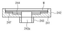
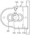
진공 플레이트(240)는 지지 플레이트(210)의 상부에 이격 배치되며, 후술할 구동 부재(250)에 의해 상하 이동한다. 도 5 및 도 6에 도시된 바와 같이, 진공 플레이트(240)는 원판 형상의 하부 벽(241)과, 하부 벽(241)의 가장자리로부터 상측으로 연장된 측벽(242)을 가진다. 하부 벽(241) 및 측벽(242)에는 홀들(245,246)이 관통 형성된다. 홀들(245,246)은 지지 플레이트(210)의 지지 핀들(214)과 척킹 핀들(216)에 대응하는 위치에 형성되며, 진공 플레이트(240)의 상하 이동시 지지 플레이트(210)의 지지 핀들(214)과 척킹 핀들(216)이 삽입된다. 하부 벽(241)의 중앙에는 개구부(243a)가 관통 형성되고, 개구부(243a)의 가장자리로부터 하부 벽(241) 의 하측으로 측벽(243)이 연장된다. 그리고 하부 벽(241)의 상면에는 개구부(243a)를 중심으로 방사상으로 그루브들(244)이 형성되며, 그루브들(244)은 개구부(243a)와 통하도록 형성된다.The
진공 플레이트(240)의 하부 벽(241) 상면에는 기판이 놓이고, 기판은 그루브들(244)을 통해 형성된 음압에 의해 진공 플레이트(240)에 진공 흡착된다. 이때, 진공 플레이트(240)의 측벽(242)은 진공 흡착된 기판이 진공 플레이트(240)로부터 이탈하는 것을 방지할 수 있으며, 측벽(242)은 청구항에 따라서는 이탈 방지 턱이라고도 한다.A substrate is placed on an upper surface of the
진공 플레이트(240)의 하부 벽(241) 상면에는 탄성 재질의 완충 부재(247)가 설치된다. 완충 부재는 실리콘 또는 불소 고무 등의 재질로 구비될 수 있다. 진공 플레이트(240)의 하부 벽(242)과 이에 진공 흡착된 기판의 사이에 파티클과 같은 이물질이 존재할 경우, 기판은 이물질에 의해 변형되어 기판의 평탄도가 저해될 수 있다. 기판의 평탄도가 저해된 상태에서 기판의 연마 공정을 진행하면, 기판 평면상의 높이 차에 의해 기판이 고르게 연마될 수 없다. 완충 부재(247)는 이러한 문제점을 해결하기 위한 것으로, 기판과 진공 플레이트(240) 사이에 이물질이 존재하더라도, 연마 공정시 기판에 가해지는 압력에 의해 이물질이 탄성 재질의 완충 부재로 함몰되기 때문에 기판의 평탄도를 고르게 유지할 수 있다.An
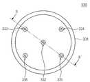
지지 플레이트(210)의 상면 중심부에는 백 노즐 어셈블리(330)가 설치되며, 지지 플레이트(210)와 백 노즐 어셈블리(330) 사이의 이격 공간으로 진공 플레이 트(240)의 측벽(243)이 상하 이동 가능하게 삽입 설치된다.The
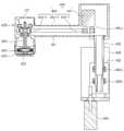
백 노즐 어셈블리(330)는 기판(W)의 하면으로 세정액을 공급하거나, 기판을 진공 흡착하기 위한 음압을 제공한다. 백 노즐 어셈블리(330)는 지지 플레이트(210)의 상면에 돌출되도록 설치된 노즐 몸체(331)를 가진다. 노즐 몸체(331)에는, 도 7에 도시된 바와 같이, 세정액 공급 부재(332,333), 린스액 공급 부재(334), 건조 가스 공급 부재(336) 및 배기 부재(335)가 제공된다. 세정액 공급 부재(332,333)는 기판의 하면으로 세정액을 분사하고, 린스액 공급 부재(334)는 기판의 하면으로 린스액을 분사하며, 건조 가스 공급 부재(336)는 기판의 하면으로 건조 가스를 분사한다. 그리고, 배기 부재(335)는 기판 하면의 공기를 흡입하여 기판을 진공 흡착하기 위한 음압을 제공한다. 도 8에 도시된 바와 같이, 세정액 공급 부재(332,333), 린스액 공급 부재(334), 건조 가스 공급 부재(336) 및 배기 부재(335)는 노즐 몸체(331)에 삽입 설치되는 튜브 형상의 노즐로 제공될 수 있다.The
구동 부재(250)는 도 3에 도시된 바와 같이 기판의 연마 공정 시에는 진공 플레이트(240)를 상측으로 이동시켜 진공 플레이트(240)가 기판을 지지하도록 하고, 도 4에 도시된 바와 같이 기판의 후-세정 공정 시에는 진공 플레이트(240)를 하측으로 이동시켜 지지 플레이트(210)가 기판을 지지하도록 한다.The driving
구동 부재(250)는 상부 자석 부재(251), 하부 자석 부재(253), 연결 부재(255), 그리고 직선 구동기(257)를 포함한다. 상부 및 하부 자석 부재(251,253)는 링 형상을 가지며, 회전 축(220)을 둘러싸도록 지지 플레이트(210)의 아래에 상 하 방향으로 배치된다. 상부 및 하부 자석 부재(251,253)에는 자석들(252,254)이 각각 설치되며, 자석들(252,254)은 서로 간에 자기적 반발력이 작용하도록 자극이 배열된다.The driving
연결 부재(255)는 봉 형상을 가지며, 지지 플레이트(210)에 상하 방향으로 관통 형성된 홀(213)에 삽입된다. 연결 부재(255)의 일단은 진공 플레이트(240)의 하부 벽(241)에 연결되고, 연결 부재(255)의 타단은 상부 자석 부재(251)에 연결된다. 그리고 하부 자석 부재(253)에는 하부 자석 부재(253)를 상하 방향으로 직선 이동시키는 직선 구동기(257)가 연결된다.The
이와 같은 구성에 의해, 직선 구동기(257)가 하부 자석 부재(253)를 상측으로 이동시키면, 하부 자석 부재(253)와의 사이에 자기적 반발력이 작용하는 상부 자석 부재(251)가 상측으로 이동되고, 결과적으로 연결 부재(255)에 의해 상부 자석 부재(251)에 연결된 진공 플레이트(240)가 상측으로 이동된다. 이 상태에서 진공 플레이트(240) 상에 기판이 로딩되고, 백 노즐 어셈블리(330)의 배기 부재(335)에 의해 기판 하부에 음압이 형성됨으로써 기판이 진공 흡착된다. 이후 후술할 연마 헤드(420)를 기판의 상부로 이동시키고, 연마 헤드(420)에 장착된 연마 패드(423)를 이용하여 기판의 연마 공정을 진행한다.With this configuration, when the
연마 공정이 완료된 후, 기판의 상하면에 대해 후-세정 공정이 진행된다. 직선 구동기(257)는 하부 자석 부재(253)를 하측으로 이동시킨다. 이때, 상부 자석 부재(251)는 지지 플레이트(210)와 상부 자석 부재(251)의 사이에 설치된 탄성 부재의 탄성 반발력에 의해 하측으로 이동되고, 결과적으로 연결 부재(255)에 의해 상부 자석 부재(251)에 연결된 진공 플레이트(240)가 하측으로 이동된다. 진공 플레이트(240)가 하측으로 이동됨에 따라, 기판은 지지 플레이트(210)의 척 부재들(214,216)에 의해 지지된다. 이 상태에서 세정 유닛(310)이 기판(W)의 상면에 세정액을 공급하고, 세정 유닛(320)이 기판(W)의 상면에 공급된 세정액에 초음파를 인가하여 기판의 상면을 세정한다. 또한, 이와 동시에 백 노즐 어셈블리(330)의 세정액 공급 부재(332)가 기판의 하면에 세정액을 공급하여 기판의 하면을 세정한다.After the polishing process is completed, the post-cleaning process is performed on the upper and lower surfaces of the substrate. The
한편, 본 발명에 따른 매엽식 기판 세정 장치에는 하부 자석 부재(253)가 연마 공정 또는 세정 공정에 따라 기설정된 높이로 상하 이동하였는가의 여부를 검출하는 감지 부재(260)가 제공될 수 있다. 감지 부재(260)로는 광 센서 등 다양한 센서가 사용될 수 있다. 감지 부재(260)는 하부 자석 부재(253)의 상승 위치에 대응하는 높이와 하부 자석 부재(253)의 하강 위치에 대응하는 높이에 설치될 수 있다. 그리고 하부 자석 부재(253)의 하부에는 꺾쇠 형상의 로드(262)가 설치될 수 있다. 하부 자석 부재(253)의 상하 이동에 따라 로드(262)의 단부가 하부 자석 부재(253)의 상승 위치에 대응하는 높이 또는 하부 자석 부재(253)의 하강 위치에 대응하는 높이에 위치하고, 이때 감지 부재(260)가 로드(262) 단부의 위치를 검출함으로써, 하부 자석 부재(253)의 상하 이동 여부를 검출할 수 있다.Meanwhile, the sheet type substrate cleaning apparatus according to the present invention may be provided with a
이상에서는 지지 플레이트가 고정되고, 진공 플레이트가 상하 이동하는 기판 지지 유닛을 예로 들어 설명하였으나, 이와 반대로 진공 플레이트가 고정되고, 지지 플레이트가 상하 이동할 수 있다.In the above description, the support plate is fixed and the substrate support unit in which the vacuum plate moves up and down has been described as an example. On the contrary, the vacuum plate is fixed and the support plate can move up and down.
도 9는 본 발명의 다른 실시 예에 따른 기판 지지 유닛을 이용하여 기판을 연마하는 공정을 보여주는 도면이고, 도 10은 본 발명의 다른 실시 예에 따른 기판 지지 유닛을 이용하여 기판을 세정하는 공정을 보여주는 도면이다.9 is a view illustrating a process of polishing a substrate using a substrate support unit according to another embodiment of the present invention, and FIG. 10 illustrates a process of cleaning a substrate using a substrate support unit according to another embodiment of the present invention. Figure showing.
도 9 및 도 10을 참조하면, 기판 지지 유닛(200)은 진공 플레이트(212'), 회전 축(220'), 회전 구동부(230'), 지지 플레이트(251') 그리고 구동 부재를 포함한다. 진공 플레이트(212')는 도 9에 도시된 바와 같이 기판의 연마 공정 진행시 기판을 지지하고, 지지 플레이트(251')는 도 10에 도시된 바와 같이 기판의 후-세정 공정 진행시 기판을 지지한다. 구동 부재(250')는 기판의 연마 공정 시에는 지지 플레이트(251')를 하측으로 이동시켜 진공 플레이트(212')가 기판을 지지하도록 하고, 기판의 후-세정 공정 시에는 지지 플레이트(251')를 상측으로 이동시켜 지지 플레이트(251')가 기판을 지지하도록 한다.9 and 10, the
진공 플레이트(212')는 원판 형상을 가진다. 진공 플레이트(212')의 중심부에는 백 노즐 어셈블리가 설치되고, 진공 플레이트(212')의 상면에는 기판의 진공 흡착을 위한 그루브들(244')이 형성된다. 백 노즐 어셈블리의 배기 부재(335)는 기판의 하면과 그루브들(244')에 의해 형성된 공간 내의 공기를 흡입하여 기판을 진공 흡착하기 위한 음압을 제공한다. 진공 플레이트(212')에는 후술할 지지 플레이트(251')의 지지 핀들(214')이 삽입되는 홀들(213')이 관통 형성된다. 진공 플레이트(212')의 하부에는 회전 축(220')이 연결되고, 회전 축(220')은 그 하단에 연결된 회전 구동부(230')에 의해 회전된다. 회전 구동부(230')는 모터 등으로 마련될 수 있다.The
지지 플레이트(251')는 진공 플레이트(212')의 하부에 이격 배치된다. 지지 플레이트(251')의 상부 면에는 기판(W)을 클램핑(Clamping)하는 척 부재들(214',216')이 설치된다. 척 부재들(214',216')은 지지 핀들(214')과 척킹 로드들(216')을 포함한다. 지지 핀들(214')은 지지 플레이트(251')의 상면에 일정 배열로 배치되며, 진공 플레이트(212')에 형성된 홀(213')에 삽입된다. 척킹 로드들(216')은 수직부(216'a)와 수평부(216'b)를 가지는 L자 형상의 로드로 구비될 수 있으며, 지지 핀들(214')의 외 측에 회전 가능하게 힌지 결합된다. 수직부(216'a)를 기준으로 수평부(216'b)의 반대 측에는 카운터 웨이트(216'c)가 설치된다. 카운터 웨이트(216'c)는 척킹 로드들(216')의 수직부(216'a)가 외향 경사진 초기 상태에 놓이도록 척킹 로드들(216')을 회전시킨다. 그리고, 진공 플레이트(212')의 하면에는 지지 플레이트(251')의 승강시 척킹 로드들(216')의 수평부(216'b)를 가압하도록 가압 부재(215')가 돌출 형성된다. 지지 플레이트(251')가 승강하면서 가압 부재(215')가 척킹 로드들(216')의 수평부(216'b)를 가압하면, 척킹 로드들(216')의 수직부(216'a)는 내측으로 회전하여 기판의 측면을 지지하고, 이때 지지 핀들(214')은 기판의 하면을 지지한다.The
진공 플레이트(212')에 연결된 회전 축(220')에는 LM 가이드와 같은 가이드 부재(255')가 설치된다. 가이드 부재(255')에는 지지 플레이트(251')가 연결되며, 가이드 부재(255')는 지지 플레이트(251')의 상하 방향 이동을 안내한다. 그리고, 진공 플레이트(212')와 지지 플레이트(251')의 사이에는 상호 간에 탄성 반발력이 작용하도록 탄성 부재(256')가 설치된다.A rotating member 220 'connected to the vacuum plate 212' is provided with a guide member 255 'such as an LM guide. The support plate 251 'is connected to the guide member 255', and the guide member 255 'guides the vertical movement of the support plate 251'. An
구동 부재는 지지 플레이트(251)에 설치된 상부 자석(252')과, 상부 자석(252')과 마주보도록 배치된 하부 자석(253')을 포함한다. 상부 자석(252')의 자극과 하부 자석(253')의 자극은 서로 간에 자기적 반발력이 작용하도록 배열된다. 하부 자석(253')은 링 형상의 하부 자석 부재(254')에 의해 지지되며, 하부 자석 부재(254')는 직선 구동기(257')에 의해 상하 방향으로 직선 이동된다.The driving member includes an upper magnet 252 'installed on the
도 9에 도시된 바와 같이, 직선 구동기(257')가 하부 자석 부재(253')를 하측으로 이동시키면, 진공 플레이트(212')와 지지 플레이트(251')의 사이에 설치된 탄성 부재(256')의 탄성 반발력에 의해 지지 플레이트(251')가 하측으로 이동된다. 이 상태에서 진공 플레이트(251') 상에 기판이 로딩되고, 백 노즐 어셈블리(330)의 배기 부재(335)에 의해 기판 하부에 음압이 형성됨으로써 기판이 진공 흡착된다. 이후 후술할 연마 헤드(420)를 기판의 상부로 이동시키고, 연마 헤드(420)에 장착된 연마 패드(423)를 이용하여 기판의 연마 공정을 진행한다.As shown in Fig. 9, when the linear driver 257 'moves the lower magnet member 253' downward, the elastic member 256 'provided between the vacuum plate 212' and the support plate 251 '. The supporting plate 251 'is moved downward by the elastic repulsive force. In this state, the substrate is loaded on the
연마 공정이 완료된 후, 기판의 상하면에 대해 후-세정 공정이 진행된다. 도 10에 도시된 바와 같이 직선 구동기(257')는 하부 자석 부재(254')를 상측으로 이동시킨다. 이때, 상부 자석(252')과 하부 자석(253') 간에 작용하는 자기적 반발력에 의해 지지 플레이트(251')가 상측으로 이동된다. 지지 플레이트(251')가 상측으로 이동됨에 따라, 가압 부재(215')가 척킹 로드(216')의 수평부(216'b)를 가압하고, 이에 의해 척킹 로드(216')의 수직부(216'a)가 내측으로 회전하여 기판의 측면 을 지지한다. 그리고, 이때 지지 핀들(214')은 기판의 하면을 지지한다. 이 상태에서 세정 유닛(310)이 기판(W)의 상면에 세정액을 공급하고, 세정 유닛(320)이 기판(W)의 상면에 공급된 세정액에 초음파를 인가하여 기판의 상면을 세정한다. 또한, 이와 동시에 백 노즐 어셈블리(330)의 세정액 공급 부재(332)가 기판의 하면에 세정액을 공급하여 기판의 하면을 세정한다.After the polishing process is completed, the post-cleaning process is performed on the upper and lower surfaces of the substrate. As shown in FIG. 10, the
다음으로, 상기와 같은 구성을 가지는 기판 지지 유닛에 고정된 기판을 연마하는 연마 유닛(400)에 대해 설명한다.Next, the polishing
도 11은 도 1의 연마 유닛의 사시도이고, 도 12는 도 11의 연마 유닛의 측단면도이며, 도 13는 도 12의 연마 헤드를 확대하여 보여주는 도면이다.FIG. 11 is a perspective view of the polishing unit of FIG. 1, FIG. 12 is a side cross-sectional view of the polishing unit of FIG. 11, and FIG. 13 is an enlarged view of the polishing head of FIG. 12.
연마 유닛(400)은 화학적 기계적 방법으로 기판 표면을 평탄화하는 연마 공정을 진행한다. 도 11 내지 도 13를 참조하면, 연마 유닛(400)은 연마 헤드(420)와, 연마 헤드(420)를 동작 모드에 따라 구동시키기 위한 제 1 , 제 2 및 제 3 구동 부재(440,460,480)를 포함한다. 연마 헤드(420)에는 기판을 연마하는 연마 패드(423)가 장착된다. 제 1 구동 부재(440)는 연마 공정의 진행시 연마 패드(423)를 자기 중심 축을 기준으로 회전시킨다. 제 2 구동 부재(460)는 연마 헤드(420)를 스윙 동작시키기 위해 연마 헤드(420)를 수평면상에서 이동시킨다. 제 3 구동 부재(480)는 연마 헤드(420)를 상하 방향으로 이동시킨다.The polishing
연마 헤드(420)는 하부가 개방된 원통 형상의 하우징(421)을 가진다. 하우징(421)의 개방된 하부에는 판 형상의 연마 패드 홀더(422)가 설치되며, 연마 패드 홀더(422)의 하면에는 연마 패드(423)가 결합된다. 연마 패드(423)는 금속 재질의 플레이트(424)의 일면에 부착될 수 있으며, 연마 패드 홀더(422)에는 금속 플레이트(424)의 다른 일 면이 연마 패드 홀더(422)에 탈착 가능하게 결합되도록 금속 플레이트(424)에 자력을 작용시키는 자석 부재(422a)가 내장될 수 있다.The polishing
연마 패드 홀더(422)의 상부 면에는 벨로우즈(425)가 설치되고, 벨로우즈(425)는 공압 부재(426)에 의해 작용되는 공기 압력에 의해 상하 방향으로 신축될 수 있다. 벨로우즈(425)는 연마 공정의 진행시 연마 패드(423)가 기판(W)에 밀착되도록 신장될 수 있으며, 연마 패드(423)가 기판(W)에 밀착된 상태에서 연마 공정이 진행되면 연마 공정이 균일하게 그리고 보다 효율적으로 진행될 수 있다.A bellows 425 is installed on the upper surface of the
공압 부재(426)는 벨로우즈(425)의 상부에 연결되며, 속이 빈 중공 축 형상의 축 부재로 구비될 수 있다. 공압 부재(426)는 길이 방향이 연직 방향을 향하도록 제공될 수 있으며, 베어링(427a,427b)에 의해 회전 가능하게 지지된다. 공압 부재(426)에는 공기를 공급하는 에어 라인(미도시)이 연결되고, 에어 라인(미도시) 상에는 에어 라인(미도시)을 개폐하는 밸브(미도시)와, 공기의 공급 유량을 조절하는 유량계(미도시)가 설치될 수 있으며, 이들의 구성은 관련 기술 분야의 당업자에게 자명한 사항이므로 이에 대한 상세한 설명은 생략한다.The
제 1 구동 부재(440)는 연마 공정의 진행시 연마 패드(423)를 자기 중심 축을 기준으로 회전시킨다. 제 1 구동 부재(440)는 회전력을 제공하는 제 1 구동 모터(441)와, 제 1 구동 모터(441)의 회전력을 연마 패드(423)로 전달하는 제 1 벨트-풀리 어셈블리(443)를 포함한다. 제 1 벨트-풀리 어셈블리(443)는 제 1 구동 풀 리(443-1), 제 1 종동 풀리(443-2) 및 제 1 벨트(443-3)의 조합으로 이루어질 수 있다. 제 1 구동 풀리(443-1)는 제 1 구동 모터(411)의 회전 축(411a)에 설치된다. 제 1 종동 풀리(443-2)는 중공 축 형상의 공압 부재(426)의 외 측면에 설치된다. 제 1 벨트(443-3)는 제 1 구동 풀리(443-1)와 제 1 종동 풀리(443-2)에 감긴다. 여기서, 제 1 구동 풀리(443-1)가 설치된 제 1 구동 모터(441)는 후술할 제 2 구동 부재(460)의 스윙 암(461)의 일단 내부에 설치되고, 제 1 벨트(443-3)는 스윙 암(461)의 길이 방향을 따라 스윙 암(461)의 내부를 통해 제 1 구동 풀리(443-1)와 제 1 종동 풀리(443-2)에 감길 수 있다.The
제 1 구동 모터(441)의 회전력은 벨트-풀리 어셈블리(443)에 의해 공압 부재(426)로 전달되고, 공압 부재(426)가 회전함에 따라 공압 부재(426)의 아래에 순차적으로 결합되어 있는 벨로우즈(425), 연마 패드 홀더(422) 및 연마 패드(423)가 회전된다. 이때, 제 1 구동 부재(440)의 제 1 구동 모터(441)는 선택적으로 시계 방향의 회전력 또는 반시계 방향의 회전력을 제공할 수 있으며, 이에 따라 도 14a 및 도 14b에 도시된 바와 같이 연마 패드(423)가 시계 방향 또는 반시계 방향으로 회전할 수 있다. 이와 같이 연마 패드(423)의 회전 방향을 시계 방향 또는 반시계 방향으로 가변시킬 수 있게 됨으로써, 연마 패드(423)를 기판(W)의 회전 방향과 동일한 방향 또는 기판(W)의 회전 방향에 반대 방향으로 회전시키면서 선택적으로 연마 공정을 진행할 수 있다.The rotational force of the
제 2 구동 부재(460)는 연마 헤드(420)를 기판상에서 스윙 동작시키기 위해 연마 헤드(420)를 수평면상에서 이동시킨다. 제 2 구동 부재(460)는 스윙 암(461), 수직 암(462), 제 2 구동 모터(463), 그리고 제 2 벨트-풀리 어셈블리(464)를 포함한다. 스윙 암(461)은 연마 헤드(420)의 하우징(421) 일 측에 수평 방향으로 결합되고, 수직 암(462)은 스윙 암(461)의 타단에 수직하게 아래 방향으로 결합된다. 제 2 구동 모터(463)는 제 2 벨트-풀리 어셈블리(464)를 통해 수직 암(462)에 회전력을 제공한다. 제 2 벨트-풀리 어셈블리(464)는 제 2 구동 풀리(464-1), 제 2 종동 풀리(464-2) 및 제 2 벨트(464-3)의 조합으로 이루어질 수 있다. 제 1 구동 풀리(464-1)는 제 2 구동 모터(463)의 회전 축에 설치된다. 제 2 종동 풀리(464-2)는 수직 암(462)의 외 측면에 설치된다. 제 2 벨트(464-3)는 제 2 구동 풀리(464-1)와 제 2 종동 풀리(464-2)에 감긴다.The
제 2 구동 모터(463)의 회전력은 제 2 벨트-풀리 어셈블리(464)에 의해 수직 암(462)으로 전달되고, 수직 암(462)이 자기 중심축을 기준으로 회전함에 따라 스윙 암(461)이 수직 암(462)을 중심으로 스윙 동작한다. 이에 따라 연마 패드(423)가 장착된 연마 헤드(420)가 원형의 곡선 궤적을 따라 이동한다.The rotational force of the
제 3 구동 부재(480)는 연마 헤드(420)를 상하 방향으로 이동시킨다. 제 3 구동 부재(480)는 지지 블록(482), 가이드 부재(484), 그리고 직선 구동기(486)를 포함한다. 지지 블록(482)은 수직 암(462)을 지지하며, 수직 암(462)은 베어링(482a,482b)에 의해 회전 가능하게 지지된다. 직선 구동기(486)는 지지 블록(482)을 상하 방향으로 직선 이동시키기 위한 구동력을 제공하며, 직선 구동 기(486)로는 실린더 부재 또는 리니어 모터와 같은 직선 구동 부재가 사용될 수 있다. 가이드 부재(484)는 지지 블록(482)의 직선 이동을 안내한다.The
직선 구동기(486)의 직선 구동력은 지지 블록(482)에 전달되고, 지지 블록(482)에 지지된 수직 암(462)이 지지 블록(482)과 함께 상하 방향으로 이동함에 따라 연마 패드(423)가 장착된 연마 헤드(420)가 상하 방향으로 이동한다.The linear driving force of the
연마 패드(423)를 이용하여 기판의 연마 공정을 반복적으로 진행하는 경우, 주기적으로 연마 패드(423)의 표면을 연마하여 연마 패드(423)의 표면 조도를 조절하여야 한다. 이를 위해, 도 1에 도시된 바와 같이, 처리실(10) 내의 연마 유닛(400)에 인접한 위치에 패드 컨디셔닝 유닛(500)이 구비된다.When the polishing process of the substrate is repeatedly performed using the
도 15은 도 1의 패드 컨디셔닝 유닛의 사시도이고, 도 16은 도 15의 패드 컨디셔닝 유닛의 측단면도이다. 그리고 도 17 및 도 18은 패드 컨디셔닝 유닛의 동작 상태를 보여주는 도면들이다.15 is a perspective view of the pad conditioning unit of FIG. 1, and FIG. 16 is a side cross-sectional view of the pad conditioning unit of FIG. 15. 17 and 18 are views illustrating an operating state of the pad conditioning unit.
도 15 내지 도 18을 참조하면, 패드 컨디셔닝 유닛(500)은 연마 패드(423)가 장착된 연마 헤드(420)의 단부가 수용되는 상부가 개방된 통 형상의 처리조(510)를 가진다. 처리조(510)는 바닥 벽(512)과, 바닥 벽(512)의 가장자리로부터 상측으로 연장된 측벽(514)을 가지며, 바닥 벽(512)의 하부에는 지지 프레임(516)이 제공된다. 처리조(510)의 바닥 벽(512)은 제 1 높이에 위치한 제 1 바닥 벽(512a)과, 제 1 바닥 벽(512a)보다 낮은 제 2 높이로 단차진 제 2 바닥 벽(512b)으로 이루어질 수 있다.15 to 18, the
처리조(510)의 제 1 바닥 벽(512a)에는 다이아몬드 컨디셔너(520)가 설치된다. 다이아몬드 컨디셔너(520)는 연마 패드(423)와 접촉하여 연마 패드(423)의 표면을 연마하기 위한 것으로, 환형 또는 원형의 다이아몬드 컨디셔너(520)가 제공될 수 있다. 그리고, 다이아몬드 컨디셔너(520)는 처리조(510)의 제 1 바닥 벽(512a)에 대응하는 크기를 가질 수 있으며, 또한 처리조(510)의 제 1 바닥 벽(512a)의 크기보다 작은 크기로 복수 개가 제공될 수도 있다.The
그리고, 처리조(510)에는 연마 패드(423)의 연마 진행 중 생성된 이물질을 제거하기 위해 처리조(510)의 제 1 바닥벽(512a)으로 탈이온수를 공급하기 위한 탈이온수 공급 부재(530,540)가 설치된다. 제 1 탈이온수 공급 부재(530)는 제 1 바닥 벽(512a)을 통해 처리조(510) 내로 탈이온수를 공급하도록 제 1 바닥 벽(512a)에 연결되며, 제 2 탈이온수 공급 부재(540)는 제 1 바닥 벽(512a)의 상측에서 제 1 바닥 벽(512a)을 향해 탈이온수를 공급하도록 처리조(510)의 일 측에 설치된다. 제 1 및 제 2 탈이온수 공급 부재(530,540)로부터 처리조(510)로 공급된 탈이온수는 제 1 바닥 벽(512a)을 타고 흐르면서 이물질을 제거하고, 이후 제 1 바닥 벽(512a) 보다 낮은 높이로 단차진 제 2 바닥 벽(512b)으로 이물질이 혼입된 탈이온수가 유입된다. 제 2 바닥 벽(512b)으로 유입된 탈이온수는 제 2 바닥 벽(512b)에 연결된 배수 부재(550)를 통해 외부로 배출된다.In addition, deionized
연마 패드(423)의 연마 공정은, 도 17에 도시된 바와 같이, 연마 헤드(420)가 처리조(510)에 수용된 상태에서 진행된다. 이때, 제 3 구동 부재(도 11의 도면 참조 번호 480)는 처리조(510)에 수용된 연마 헤드(420)를 상하 방향으로 이동시켜 연마 패드(423)를 다이아몬드 컨디셔너(520)에 접촉시킨다. 이 상태에서, 도 18에 도시된 바와 같이, 제 1 구동 부재(도 11의 도면 참조 번호 440)는 연마 패드(423)를 회전시키고, 제 2 구동 부재(도 11의 도면 참조 번호 460)는 연마 헤드(420)를 수평면상에서 이동시켜 다이아몬드 컨디셔너(520) 상에서 연마 패드(423)를 스캐닝시킨다. 이때, 제 1 및 제 2 탈이온수 공급 부재(530,540)는 처리조(510) 내로 탈이온수를 공급하고, 탈이온수는 연마 패드(423)의 연마 중 발생하는 이물질을 제거한 후 배수 부재(550)를 통해 외부로 배출된다.The polishing process of the
이상의 설명은 본 발명의 기술 사상을 예시적으로 설명한 것에 불과한 것으로서, 본 발명이 속하는 기술 분야에서 통상의 지식을 가진 자라면 본 발명의 본질적인 특성에서 벗어나지 않는 범위에서 다양한 수정 및 변형이 가능할 것이다. 따라서, 본 발명에 개시된 실시 예들은 본 발명의 기술 사상을 한정하기 위한 것이 아니라 설명하기 위한 것이고, 이러한 실시 예에 의하여 본 발명의 기술 사상의 범위가 한정되는 것은 아니다. 본 발명의 보호 범위는 아래의 청구범위에 의하여 해석되어야 하며, 그와 동등한 범위 내에 있는 모든 기술 사상은 본 발명의 권리범위에 포함되는 것으로 해석되어야 할 것이다.The foregoing description is merely illustrative of the technical idea of the present invention, and various changes and modifications may be made by those skilled in the art without departing from the essential characteristics of the present invention. Therefore, the embodiments disclosed in the present invention are not intended to limit the technical idea of the present invention but to describe the present invention, and the scope of the technical idea of the present invention is not limited by these embodiments. The protection scope of the present invention should be interpreted by the following claims, and all technical ideas within the equivalent scope should be interpreted as being included in the scope of the present invention.
이하에 설명된 도면들은 단지 예시의 목적을 위한 것이고, 본 발명의 범위를 제한하기 위한 것이 아니다.The drawings described below are for illustrative purposes only and are not intended to limit the scope of the invention.
도 1은 본 발명에 따른 매엽식 기판 연마 장치의 사시도,1 is a perspective view of a sheet type substrate polishing apparatus according to the present invention,
도 2는 도 1의 처리 용기와 기판 지지 유닛의 측단면도,2 is a side cross-sectional view of the processing vessel and substrate support unit of FIG. 1;
도 3은 본 발명의 일 실시 예에 따른 기판 지지 유닛을 이용하여 기판을 연마하는 공정을 보여주는 도면,3 is a view showing a process of polishing a substrate using a substrate support unit according to an embodiment of the present invention;
도 4는 본 발명의 일 실시 예에 따른 기판 지지 유닛을 이용하여 기판을 세정하는 공정을 보여주는 도면,4 is a view showing a process of cleaning a substrate using a substrate support unit according to an embodiment of the present invention;
도 5는 도 3의 진공 플레이트의 평면도,5 is a plan view of the vacuum plate of FIG.
도 6은 도 5의 A-A' 선에 따른 단면도,6 is a cross-sectional view taken along line AA ′ of FIG. 5;
도 7은 도 3의 백 노즐 어셈블리의 평면도,7 is a plan view of the bag nozzle assembly of FIG.
도 8은 도 7의 B-B' 선에 따른 단면도,8 is a cross-sectional view taken along line BB ′ of FIG. 7;
도 9는 본 발명의 다른 실시 예에 따른 기판 지지 유닛을 이용하여 기판을 연마하는 공정을 보여주는 도면,9 is a view showing a process of polishing a substrate using a substrate support unit according to another embodiment of the present invention;
도 10은 본 발명의 다른 실시 예에 따른 기판 지지 유닛을 이용하여 기판을 세정하는 공정을 보여주는 도면,10 is a view showing a process of cleaning a substrate using a substrate support unit according to another embodiment of the present invention;
도 11은 도 1의 연마 유닛의 사시도,11 is a perspective view of the polishing unit of FIG.
도 12는 도 11의 연마 유닛의 측단면도,12 is a side cross-sectional view of the polishing unit of FIG. 11;
도 13는 도 12의 연마 헤드를 확대하여 보여주는 도면,FIG. 13 is an enlarged view of the polishing head of FIG. 12; FIG.
도 14a 및 도 14b는 연마 패드를 이용한 연마 공정의 예들을 보여주는 도면,14A and 14B show examples of a polishing process using a polishing pad,
도 15은 도 1의 패드 컨디셔닝 유닛의 사시도,15 is a perspective view of the pad conditioning unit of FIG. 1, FIG.
도 16은 도 15의 패드 컨디셔닝 유닛의 측단면도,16 is a side cross-sectional view of the pad conditioning unit of FIG. 15;
도 17는 패드 컨디셔닝 유닛의 동작 상태를 보여주는 단면도,17 is a sectional view showing an operating state of the pad conditioning unit,
도 18은 패드 컨디셔닝 유닛의 동작 상태를 보여주는 평면도이다.18 is a plan view showing an operating state of the pad conditioning unit.
< 도면의 주요 부분에 대한 부호의 설명 ><Description of Symbols for Main Parts of Drawings>
100 : 처리 용기200 : 기판 지지 유닛100: processing container 200: substrate support unit
210 : 지지 플레이트220 : 회전 축210: support plate 220: axis of rotation
230 : 회전 구동부240 : 진공 플레이트230: rotary drive unit 240: vacuum plate
250 : 구동 부재310,320 : 세정 유닛250: drive member 310,320: cleaning unit
400 : 연마 유닛500 : 패드 컨디셔닝 유닛400: polishing unit 500: pad conditioning unit
Claims (33)
Translated fromKoreanPriority Applications (5)
| Application Number | Priority Date | Filing Date | Title |
|---|---|---|---|
| KR1020080062444AKR101036605B1 (en) | 2008-06-30 | 2008-06-30 | Substrate support unit and sheet type substrate polishing apparatus using the same |
| JP2008295492AJP5004059B2 (en) | 2008-06-30 | 2008-11-19 | Single substrate polishing machine |
| CN2008101765518ACN101618520B (en) | 2008-06-30 | 2008-11-19 | Substrate supporting unit and single type substrate polishing apparatus using the same |
| US12/273,829US8113918B2 (en) | 2008-06-30 | 2008-11-19 | Substrate supporting unit and single type substrate polishing apparatus using the same |
| TW097144989ATWI404166B (en) | 2008-06-30 | 2008-11-20 | Substrate supporting unit, single type substrate polishing apparatus using the unit, and substrate polishing method using the apparatus |
Applications Claiming Priority (1)
| Application Number | Priority Date | Filing Date | Title |
|---|---|---|---|
| KR1020080062444AKR101036605B1 (en) | 2008-06-30 | 2008-06-30 | Substrate support unit and sheet type substrate polishing apparatus using the same |
Publications (2)
| Publication Number | Publication Date |
|---|---|
| KR20100002523A KR20100002523A (en) | 2010-01-07 |
| KR101036605B1true KR101036605B1 (en) | 2011-05-24 |
Family
ID=41448017
Family Applications (1)
| Application Number | Title | Priority Date | Filing Date |
|---|---|---|---|
| KR1020080062444AActiveKR101036605B1 (en) | 2008-06-30 | 2008-06-30 | Substrate support unit and sheet type substrate polishing apparatus using the same |
Country Status (5)
| Country | Link |
|---|---|
| US (1) | US8113918B2 (en) |
| JP (1) | JP5004059B2 (en) |
| KR (1) | KR101036605B1 (en) |
| CN (1) | CN101618520B (en) |
| TW (1) | TWI404166B (en) |
Cited By (1)
| Publication number | Priority date | Publication date | Assignee | Title |
|---|---|---|---|---|
| KR20180077016A (en)* | 2016-12-28 | 2018-07-06 | 가부시키가이샤 스크린 홀딩스 | Substrate processing apparatus and substrate processing method |
Families Citing this family (394)
| Publication number | Priority date | Publication date | Assignee | Title |
|---|---|---|---|---|
| JP4783404B2 (en)* | 2008-07-02 | 2011-09-28 | 光洋機械工業株式会社 | Work mounting device |
| JP4783405B2 (en)* | 2008-07-02 | 2011-09-28 | 光洋機械工業株式会社 | Inclination angle adjusting device and workpiece mounting device |
| US10378106B2 (en) | 2008-11-14 | 2019-08-13 | Asm Ip Holding B.V. | Method of forming insulation film by modified PEALD |
| KR101004434B1 (en)* | 2008-11-26 | 2010-12-28 | 세메스 주식회사 | Substrate support unit, substrate polishing apparatus and method using same |
| KR101004435B1 (en)* | 2008-11-28 | 2010-12-28 | 세메스 주식회사 | Substrate Polishing Apparatus and Substrate Polishing Method Using The Same |
| US9394608B2 (en) | 2009-04-06 | 2016-07-19 | Asm America, Inc. | Semiconductor processing reactor and components thereof |
| KR101170760B1 (en)* | 2009-07-24 | 2012-08-03 | 세메스 주식회사 | Substrate polishing apparatus |
| US8802201B2 (en) | 2009-08-14 | 2014-08-12 | Asm America, Inc. | Systems and methods for thin-film deposition of metal oxides using excited nitrogen-oxygen species |
| KR101610832B1 (en)* | 2010-03-03 | 2016-04-08 | 삼성전자주식회사 | Chemical Mechanical Polishing Appratus |
| CN102528643A (en)* | 2010-12-30 | 2012-07-04 | 中芯国际集成电路制造(上海)有限公司 | Chemical mechanical polishing equipment and polishing unit thereof |
| US9312155B2 (en) | 2011-06-06 | 2016-04-12 | Asm Japan K.K. | High-throughput semiconductor-processing apparatus equipped with multiple dual-chamber modules |
| US10364496B2 (en) | 2011-06-27 | 2019-07-30 | Asm Ip Holding B.V. | Dual section module having shared and unshared mass flow controllers |
| US10854498B2 (en) | 2011-07-15 | 2020-12-01 | Asm Ip Holding B.V. | Wafer-supporting device and method for producing same |
| US20130023129A1 (en) | 2011-07-20 | 2013-01-24 | Asm America, Inc. | Pressure transmitter for a semiconductor processing environment |
| US9017481B1 (en) | 2011-10-28 | 2015-04-28 | Asm America, Inc. | Process feed management for semiconductor substrate processing |
| KR101874901B1 (en) | 2011-12-07 | 2018-07-06 | 삼성전자주식회사 | Apparatus and method for drying substrate |
| US9385020B2 (en)* | 2011-12-19 | 2016-07-05 | SCREEN Holdings Co., Ltd. | Substrate holding and rotating device, substrate treatment apparatus including the device, and substrate treatment method |
| US9659799B2 (en) | 2012-08-28 | 2017-05-23 | Asm Ip Holding B.V. | Systems and methods for dynamic semiconductor process scheduling |
| US9021985B2 (en) | 2012-09-12 | 2015-05-05 | Asm Ip Holdings B.V. | Process gas management for an inductively-coupled plasma deposition reactor |
| KR101381635B1 (en)* | 2012-09-21 | 2014-04-04 | 청진테크 주식회사 | Cleaning apparatus |
| KR101387568B1 (en)* | 2012-10-10 | 2014-04-22 | (주)에스티아이 | Rod Cassette For Solar Cell Manufacturing Process |
| US10714315B2 (en) | 2012-10-12 | 2020-07-14 | Asm Ip Holdings B.V. | Semiconductor reaction chamber showerhead |
| US20160376700A1 (en) | 2013-02-01 | 2016-12-29 | Asm Ip Holding B.V. | System for treatment of deposition reactor |
| US9589770B2 (en) | 2013-03-08 | 2017-03-07 | Asm Ip Holding B.V. | Method and systems for in-situ formation of intermediate reactive species |
| US9484191B2 (en) | 2013-03-08 | 2016-11-01 | Asm Ip Holding B.V. | Pulsed remote plasma method and system |
| CN103252713B (en)* | 2013-05-08 | 2015-12-02 | 浙江工业大学 | A kind of magnetic load wafer Ginding process and device |
| JP6190679B2 (en)* | 2013-09-24 | 2017-08-30 | 株式会社テックインテック | Substrate holding mechanism and substrate processing apparatus using the same |
| US9240412B2 (en) | 2013-09-27 | 2016-01-19 | Asm Ip Holding B.V. | Semiconductor structure and device and methods of forming same using selective epitaxial process |
| US10683571B2 (en) | 2014-02-25 | 2020-06-16 | Asm Ip Holding B.V. | Gas supply manifold and method of supplying gases to chamber using same |
| US10167557B2 (en) | 2014-03-18 | 2019-01-01 | Asm Ip Holding B.V. | Gas distribution system, reactor including the system, and methods of using the same |
| US11015245B2 (en) | 2014-03-19 | 2021-05-25 | Asm Ip Holding B.V. | Gas-phase reactor and system having exhaust plenum and components thereof |
| JP6309371B2 (en)* | 2014-07-01 | 2018-04-11 | 株式会社ディスコ | Unloading plate workpiece |
| JP6400967B2 (en)* | 2014-07-18 | 2018-10-03 | 株式会社Screenホールディングス | Substrate processing equipment |
| US10858737B2 (en) | 2014-07-28 | 2020-12-08 | Asm Ip Holding B.V. | Showerhead assembly and components thereof |
| US9890456B2 (en) | 2014-08-21 | 2018-02-13 | Asm Ip Holding B.V. | Method and system for in situ formation of gas-phase compounds |
| US10941490B2 (en) | 2014-10-07 | 2021-03-09 | Asm Ip Holding B.V. | Multiple temperature range susceptor, assembly, reactor and system including the susceptor, and methods of using the same |
| US9657845B2 (en) | 2014-10-07 | 2017-05-23 | Asm Ip Holding B.V. | Variable conductance gas distribution apparatus and method |
| US9714462B2 (en)* | 2014-10-08 | 2017-07-25 | Applied Materials, Inc. | Vacuum pre-wetting apparatus and methods |
| KR102263121B1 (en) | 2014-12-22 | 2021-06-09 | 에이에스엠 아이피 홀딩 비.브이. | Semiconductor device and manufacuring method thereof |
| US10529542B2 (en) | 2015-03-11 | 2020-01-07 | Asm Ip Holdings B.V. | Cross-flow reactor and method |
| US10276355B2 (en) | 2015-03-12 | 2019-04-30 | Asm Ip Holding B.V. | Multi-zone reactor, system including the reactor, and method of using the same |
| RU2607071C2 (en)* | 2015-03-23 | 2017-01-10 | Акционерное общество "Научно-исследовательское проектно-технологическое бюро "Онега" | Device for processed part installation on cutting machine |
| US10593554B2 (en) | 2015-04-14 | 2020-03-17 | Jun Yang | Method and apparatus for within-wafer profile localized tuning |
| US10458018B2 (en) | 2015-06-26 | 2019-10-29 | Asm Ip Holding B.V. | Structures including metal carbide material, devices including the structures, and methods of forming same |
| US10600673B2 (en)* | 2015-07-07 | 2020-03-24 | Asm Ip Holding B.V. | Magnetic susceptor to baseplate seal |
| US10083836B2 (en) | 2015-07-24 | 2018-09-25 | Asm Ip Holding B.V. | Formation of boron-doped titanium metal films with high work function |
| US9960072B2 (en) | 2015-09-29 | 2018-05-01 | Asm Ip Holding B.V. | Variable adjustment for precise matching of multiple chamber cavity housings |
| US10211308B2 (en) | 2015-10-21 | 2019-02-19 | Asm Ip Holding B.V. | NbMC layers |
| US10322384B2 (en) | 2015-11-09 | 2019-06-18 | Asm Ip Holding B.V. | Counter flow mixer for process chamber |
| JP6721967B2 (en)* | 2015-11-17 | 2020-07-15 | 株式会社荏原製作所 | Buff processing device and substrate processing device |
| US11139308B2 (en) | 2015-12-29 | 2021-10-05 | Asm Ip Holding B.V. | Atomic layer deposition of III-V compounds to form V-NAND devices |
| CN106933045B (en)* | 2015-12-30 | 2019-06-25 | 上海微电子装备(集团)股份有限公司 | A kind of auxiliary support apparatus and the photoetching machine equipment with Auxiliary support |
| US10529554B2 (en) | 2016-02-19 | 2020-01-07 | Asm Ip Holding B.V. | Method for forming silicon nitride film selectively on sidewalls or flat surfaces of trenches |
| US10468251B2 (en) | 2016-02-19 | 2019-11-05 | Asm Ip Holding B.V. | Method for forming spacers using silicon nitride film for spacer-defined multiple patterning |
| US10501866B2 (en) | 2016-03-09 | 2019-12-10 | Asm Ip Holding B.V. | Gas distribution apparatus for improved film uniformity in an epitaxial system |
| US10343920B2 (en) | 2016-03-18 | 2019-07-09 | Asm Ip Holding B.V. | Aligned carbon nanotubes |
| US9892913B2 (en) | 2016-03-24 | 2018-02-13 | Asm Ip Holding B.V. | Radial and thickness control via biased multi-port injection settings |
| US10865475B2 (en) | 2016-04-21 | 2020-12-15 | Asm Ip Holding B.V. | Deposition of metal borides and silicides |
| US10190213B2 (en) | 2016-04-21 | 2019-01-29 | Asm Ip Holding B.V. | Deposition of metal borides |
| CN105834900B (en)* | 2016-04-28 | 2019-03-26 | 浙江工业大学 | A kind of polishing workpiece vacuum fixture self-checking device |
| US10367080B2 (en) | 2016-05-02 | 2019-07-30 | Asm Ip Holding B.V. | Method of forming a germanium oxynitride film |
| US10032628B2 (en) | 2016-05-02 | 2018-07-24 | Asm Ip Holding B.V. | Source/drain performance through conformal solid state doping |
| KR102592471B1 (en) | 2016-05-17 | 2023-10-20 | 에이에스엠 아이피 홀딩 비.브이. | Method of forming metal interconnection and method of fabricating semiconductor device using the same |
| US11453943B2 (en) | 2016-05-25 | 2022-09-27 | Asm Ip Holding B.V. | Method for forming carbon-containing silicon/metal oxide or nitride film by ALD using silicon precursor and hydrocarbon precursor |
| RU172335U1 (en)* | 2016-06-28 | 2017-07-04 | Акционерное общество "Научно-исследовательское проектно-технологическое бюро "Онега" | DEVICE FOR INSTALLING THE PROCESSED PARTS ON THE METAL-CUTTING MACHINE |
| US10388509B2 (en) | 2016-06-28 | 2019-08-20 | Asm Ip Holding B.V. | Formation of epitaxial layers via dislocation filtering |
| US20180354142A1 (en)* | 2016-06-30 | 2018-12-13 | Aem Singapore Pte. Ltd. | Automated picking apparatus with magnetic repulsion for picking an object or a set of objects and method thereof |
| US10612137B2 (en) | 2016-07-08 | 2020-04-07 | Asm Ip Holdings B.V. | Organic reactants for atomic layer deposition |
| US9859151B1 (en) | 2016-07-08 | 2018-01-02 | Asm Ip Holding B.V. | Selective film deposition method to form air gaps |
| US10714385B2 (en) | 2016-07-19 | 2020-07-14 | Asm Ip Holding B.V. | Selective deposition of tungsten |
| KR102354490B1 (en) | 2016-07-27 | 2022-01-21 | 에이에스엠 아이피 홀딩 비.브이. | Method of processing a substrate |
| US9887082B1 (en) | 2016-07-28 | 2018-02-06 | Asm Ip Holding B.V. | Method and apparatus for filling a gap |
| KR102532607B1 (en) | 2016-07-28 | 2023-05-15 | 에이에스엠 아이피 홀딩 비.브이. | Substrate processing apparatus and method of operating the same |
| US9812320B1 (en) | 2016-07-28 | 2017-11-07 | Asm Ip Holding B.V. | Method and apparatus for filling a gap |
| US10395919B2 (en) | 2016-07-28 | 2019-08-27 | Asm Ip Holding B.V. | Method and apparatus for filling a gap |
| US10410943B2 (en) | 2016-10-13 | 2019-09-10 | Asm Ip Holding B.V. | Method for passivating a surface of a semiconductor and related systems |
| US10643826B2 (en) | 2016-10-26 | 2020-05-05 | Asm Ip Holdings B.V. | Methods for thermally calibrating reaction chambers |
| US11532757B2 (en) | 2016-10-27 | 2022-12-20 | Asm Ip Holding B.V. | Deposition of charge trapping layers |
| US10643904B2 (en) | 2016-11-01 | 2020-05-05 | Asm Ip Holdings B.V. | Methods for forming a semiconductor device and related semiconductor device structures |
| US10435790B2 (en) | 2016-11-01 | 2019-10-08 | Asm Ip Holding B.V. | Method of subatmospheric plasma-enhanced ALD using capacitively coupled electrodes with narrow gap |
| US10714350B2 (en) | 2016-11-01 | 2020-07-14 | ASM IP Holdings, B.V. | Methods for forming a transition metal niobium nitride film on a substrate by atomic layer deposition and related semiconductor device structures |
| US10229833B2 (en) | 2016-11-01 | 2019-03-12 | Asm Ip Holding B.V. | Methods for forming a transition metal nitride film on a substrate by atomic layer deposition and related semiconductor device structures |
| US10134757B2 (en) | 2016-11-07 | 2018-11-20 | Asm Ip Holding B.V. | Method of processing a substrate and a device manufactured by using the method |
| TWI645913B (en)* | 2016-11-10 | 2019-01-01 | 辛耘企業股份有限公司 | Liquid processing device |
| KR102546317B1 (en) | 2016-11-15 | 2023-06-21 | 에이에스엠 아이피 홀딩 비.브이. | Gas supply unit and substrate processing apparatus including the same |
| US10340135B2 (en) | 2016-11-28 | 2019-07-02 | Asm Ip Holding B.V. | Method of topologically restricted plasma-enhanced cyclic deposition of silicon or metal nitride |
| KR102762543B1 (en) | 2016-12-14 | 2025-02-05 | 에이에스엠 아이피 홀딩 비.브이. | Substrate processing apparatus |
| US11447861B2 (en) | 2016-12-15 | 2022-09-20 | Asm Ip Holding B.V. | Sequential infiltration synthesis apparatus and a method of forming a patterned structure |
| US11581186B2 (en) | 2016-12-15 | 2023-02-14 | Asm Ip Holding B.V. | Sequential infiltration synthesis apparatus |
| KR102700194B1 (en) | 2016-12-19 | 2024-08-28 | 에이에스엠 아이피 홀딩 비.브이. | Substrate processing apparatus |
| US10269558B2 (en) | 2016-12-22 | 2019-04-23 | Asm Ip Holding B.V. | Method of forming a structure on a substrate |
| US10867788B2 (en) | 2016-12-28 | 2020-12-15 | Asm Ip Holding B.V. | Method of forming a structure on a substrate |
| US11390950B2 (en) | 2017-01-10 | 2022-07-19 | Asm Ip Holding B.V. | Reactor system and method to reduce residue buildup during a film deposition process |
| CN106826516B (en)* | 2017-01-18 | 2018-10-23 | 浙江金达莱装饰工程有限公司 | A kind of polishing mechanism |
| US10655221B2 (en) | 2017-02-09 | 2020-05-19 | Asm Ip Holding B.V. | Method for depositing oxide film by thermal ALD and PEALD |
| US10468261B2 (en) | 2017-02-15 | 2019-11-05 | Asm Ip Holding B.V. | Methods for forming a metallic film on a substrate by cyclical deposition and related semiconductor device structures |
| US10529563B2 (en) | 2017-03-29 | 2020-01-07 | Asm Ip Holdings B.V. | Method for forming doped metal oxide films on a substrate by cyclical deposition and related semiconductor device structures |
| US10283353B2 (en) | 2017-03-29 | 2019-05-07 | Asm Ip Holding B.V. | Method of reforming insulating film deposited on substrate with recess pattern |
| KR102457289B1 (en) | 2017-04-25 | 2022-10-21 | 에이에스엠 아이피 홀딩 비.브이. | Method for depositing a thin film and manufacturing a semiconductor device |
| US10770286B2 (en) | 2017-05-08 | 2020-09-08 | Asm Ip Holdings B.V. | Methods for selectively forming a silicon nitride film on a substrate and related semiconductor device structures |
| US10892156B2 (en) | 2017-05-08 | 2021-01-12 | Asm Ip Holding B.V. | Methods for forming a silicon nitride film on a substrate and related semiconductor device structures |
| US10446393B2 (en) | 2017-05-08 | 2019-10-15 | Asm Ip Holding B.V. | Methods for forming silicon-containing epitaxial layers and related semiconductor device structures |
| US10504742B2 (en) | 2017-05-31 | 2019-12-10 | Asm Ip Holding B.V. | Method of atomic layer etching using hydrogen plasma |
| US10886123B2 (en) | 2017-06-02 | 2021-01-05 | Asm Ip Holding B.V. | Methods for forming low temperature semiconductor layers and related semiconductor device structures |
| KR101951006B1 (en)* | 2017-06-05 | 2019-02-27 | 레셀 주식회사 | Apparatus for mounting substrate container |
| US12040200B2 (en) | 2017-06-20 | 2024-07-16 | Asm Ip Holding B.V. | Semiconductor processing apparatus and methods for calibrating a semiconductor processing apparatus |
| US11306395B2 (en) | 2017-06-28 | 2022-04-19 | Asm Ip Holding B.V. | Methods for depositing a transition metal nitride film on a substrate by atomic layer deposition and related deposition apparatus |
| US10685834B2 (en) | 2017-07-05 | 2020-06-16 | Asm Ip Holdings B.V. | Methods for forming a silicon germanium tin layer and related semiconductor device structures |
| KR20190009245A (en) | 2017-07-18 | 2019-01-28 | 에이에스엠 아이피 홀딩 비.브이. | Methods for forming a semiconductor device structure and related semiconductor device structures |
| US11018002B2 (en) | 2017-07-19 | 2021-05-25 | Asm Ip Holding B.V. | Method for selectively depositing a Group IV semiconductor and related semiconductor device structures |
| US10541333B2 (en) | 2017-07-19 | 2020-01-21 | Asm Ip Holding B.V. | Method for depositing a group IV semiconductor and related semiconductor device structures |
| US11374112B2 (en) | 2017-07-19 | 2022-06-28 | Asm Ip Holding B.V. | Method for depositing a group IV semiconductor and related semiconductor device structures |
| US10312055B2 (en) | 2017-07-26 | 2019-06-04 | Asm Ip Holding B.V. | Method of depositing film by PEALD using negative bias |
| US10605530B2 (en) | 2017-07-26 | 2020-03-31 | Asm Ip Holding B.V. | Assembly of a liner and a flange for a vertical furnace as well as the liner and the vertical furnace |
| US10590535B2 (en) | 2017-07-26 | 2020-03-17 | Asm Ip Holdings B.V. | Chemical treatment, deposition and/or infiltration apparatus and method for using the same |
| TWI815813B (en) | 2017-08-04 | 2023-09-21 | 荷蘭商Asm智慧財產控股公司 | Showerhead assembly for distributing a gas within a reaction chamber |
| US10770336B2 (en) | 2017-08-08 | 2020-09-08 | Asm Ip Holding B.V. | Substrate lift mechanism and reactor including same |
| US10692741B2 (en) | 2017-08-08 | 2020-06-23 | Asm Ip Holdings B.V. | Radiation shield |
| US10249524B2 (en) | 2017-08-09 | 2019-04-02 | Asm Ip Holding B.V. | Cassette holder assembly for a substrate cassette and holding member for use in such assembly |
| US11139191B2 (en) | 2017-08-09 | 2021-10-05 | Asm Ip Holding B.V. | Storage apparatus for storing cassettes for substrates and processing apparatus equipped therewith |
| US11769682B2 (en) | 2017-08-09 | 2023-09-26 | Asm Ip Holding B.V. | Storage apparatus for storing cassettes for substrates and processing apparatus equipped therewith |
| US10236177B1 (en) | 2017-08-22 | 2019-03-19 | ASM IP Holding B.V.. | Methods for depositing a doped germanium tin semiconductor and related semiconductor device structures |
| USD900036S1 (en) | 2017-08-24 | 2020-10-27 | Asm Ip Holding B.V. | Heater electrical connector and adapter |
| US11830730B2 (en) | 2017-08-29 | 2023-11-28 | Asm Ip Holding B.V. | Layer forming method and apparatus |
| KR102491945B1 (en) | 2017-08-30 | 2023-01-26 | 에이에스엠 아이피 홀딩 비.브이. | Substrate processing apparatus |
| US11056344B2 (en) | 2017-08-30 | 2021-07-06 | Asm Ip Holding B.V. | Layer forming method |
| US11295980B2 (en) | 2017-08-30 | 2022-04-05 | Asm Ip Holding B.V. | Methods for depositing a molybdenum metal film over a dielectric surface of a substrate by a cyclical deposition process and related semiconductor device structures |
| KR102401446B1 (en) | 2017-08-31 | 2022-05-24 | 에이에스엠 아이피 홀딩 비.브이. | Substrate processing apparatus |
| US10607895B2 (en) | 2017-09-18 | 2020-03-31 | Asm Ip Holdings B.V. | Method for forming a semiconductor device structure comprising a gate fill metal |
| KR102630301B1 (en) | 2017-09-21 | 2024-01-29 | 에이에스엠 아이피 홀딩 비.브이. | Method of sequential infiltration synthesis treatment of infiltrateable material and structures and devices formed using same |
| US10844484B2 (en) | 2017-09-22 | 2020-11-24 | Asm Ip Holding B.V. | Apparatus for dispensing a vapor phase reactant to a reaction chamber and related methods |
| US10658205B2 (en) | 2017-09-28 | 2020-05-19 | Asm Ip Holdings B.V. | Chemical dispensing apparatus and methods for dispensing a chemical to a reaction chamber |
| US10403504B2 (en) | 2017-10-05 | 2019-09-03 | Asm Ip Holding B.V. | Method for selectively depositing a metallic film on a substrate |
| US10319588B2 (en) | 2017-10-10 | 2019-06-11 | Asm Ip Holding B.V. | Method for depositing a metal chalcogenide on a substrate by cyclical deposition |
| US10923344B2 (en) | 2017-10-30 | 2021-02-16 | Asm Ip Holding B.V. | Methods for forming a semiconductor structure and related semiconductor structures |
| US11056358B2 (en)* | 2017-11-14 | 2021-07-06 | Taiwan Semiconductor Manufacturing Co., Ltd. | Wafer cleaning apparatus and method |
| US10910262B2 (en) | 2017-11-16 | 2021-02-02 | Asm Ip Holding B.V. | Method of selectively depositing a capping layer structure on a semiconductor device structure |
| KR102443047B1 (en) | 2017-11-16 | 2022-09-14 | 에이에스엠 아이피 홀딩 비.브이. | Method of processing a substrate and a device manufactured by the same |
| US11022879B2 (en) | 2017-11-24 | 2021-06-01 | Asm Ip Holding B.V. | Method of forming an enhanced unexposed photoresist layer |
| WO2019103613A1 (en) | 2017-11-27 | 2019-05-31 | Asm Ip Holding B.V. | A storage device for storing wafer cassettes for use with a batch furnace |
| CN111344522B (en) | 2017-11-27 | 2022-04-12 | 阿斯莫Ip控股公司 | Including clean mini-environment device |
| US10290508B1 (en) | 2017-12-05 | 2019-05-14 | Asm Ip Holding B.V. | Method for forming vertical spacers for spacer-defined patterning |
| US10872771B2 (en) | 2018-01-16 | 2020-12-22 | Asm Ip Holding B. V. | Method for depositing a material film on a substrate within a reaction chamber by a cyclical deposition process and related device structures |
| KR102695659B1 (en) | 2018-01-19 | 2024-08-14 | 에이에스엠 아이피 홀딩 비.브이. | Method for depositing a gap filling layer by plasma assisted deposition |
| TWI799494B (en) | 2018-01-19 | 2023-04-21 | 荷蘭商Asm 智慧財產控股公司 | Deposition method |
| USD903477S1 (en) | 2018-01-24 | 2020-12-01 | Asm Ip Holdings B.V. | Metal clamp |
| US11018047B2 (en) | 2018-01-25 | 2021-05-25 | Asm Ip Holding B.V. | Hybrid lift pin |
| US10535516B2 (en) | 2018-02-01 | 2020-01-14 | Asm Ip Holdings B.V. | Method for depositing a semiconductor structure on a surface of a substrate and related semiconductor structures |
| USD880437S1 (en) | 2018-02-01 | 2020-04-07 | Asm Ip Holding B.V. | Gas supply plate for semiconductor manufacturing apparatus |
| US11081345B2 (en) | 2018-02-06 | 2021-08-03 | Asm Ip Holding B.V. | Method of post-deposition treatment for silicon oxide film |
| WO2019158960A1 (en) | 2018-02-14 | 2019-08-22 | Asm Ip Holding B.V. | A method for depositing a ruthenium-containing film on a substrate by a cyclical deposition process |
| US10896820B2 (en) | 2018-02-14 | 2021-01-19 | Asm Ip Holding B.V. | Method for depositing a ruthenium-containing film on a substrate by a cyclical deposition process |
| US10731249B2 (en) | 2018-02-15 | 2020-08-04 | Asm Ip Holding B.V. | Method of forming a transition metal containing film on a substrate by a cyclical deposition process, a method for supplying a transition metal halide compound to a reaction chamber, and related vapor deposition apparatus |
| US10658181B2 (en) | 2018-02-20 | 2020-05-19 | Asm Ip Holding B.V. | Method of spacer-defined direct patterning in semiconductor fabrication |
| KR102636427B1 (en) | 2018-02-20 | 2024-02-13 | 에이에스엠 아이피 홀딩 비.브이. | Substrate processing method and apparatus |
| US10975470B2 (en) | 2018-02-23 | 2021-04-13 | Asm Ip Holding B.V. | Apparatus for detecting or monitoring for a chemical precursor in a high temperature environment |
| US11473195B2 (en) | 2018-03-01 | 2022-10-18 | Asm Ip Holding B.V. | Semiconductor processing apparatus and a method for processing a substrate |
| US11629406B2 (en) | 2018-03-09 | 2023-04-18 | Asm Ip Holding B.V. | Semiconductor processing apparatus comprising one or more pyrometers for measuring a temperature of a substrate during transfer of the substrate |
| US11114283B2 (en) | 2018-03-16 | 2021-09-07 | Asm Ip Holding B.V. | Reactor, system including the reactor, and methods of manufacturing and using same |
| KR102038508B1 (en)* | 2018-03-26 | 2019-10-30 | 주식회사 케이씨텍 | Substrate processing apparatus |
| KR102646467B1 (en) | 2018-03-27 | 2024-03-11 | 에이에스엠 아이피 홀딩 비.브이. | Method of forming an electrode on a substrate and a semiconductor device structure including an electrode |
| US10510536B2 (en) | 2018-03-29 | 2019-12-17 | Asm Ip Holding B.V. | Method of depositing a co-doped polysilicon film on a surface of a substrate within a reaction chamber |
| US11230766B2 (en) | 2018-03-29 | 2022-01-25 | Asm Ip Holding B.V. | Substrate processing apparatus and method |
| US11088002B2 (en) | 2018-03-29 | 2021-08-10 | Asm Ip Holding B.V. | Substrate rack and a substrate processing system and method |
| KR102501472B1 (en) | 2018-03-30 | 2023-02-20 | 에이에스엠 아이피 홀딩 비.브이. | Substrate processing method |
| KR102600229B1 (en) | 2018-04-09 | 2023-11-10 | 에이에스엠 아이피 홀딩 비.브이. | Substrate supporting device, substrate processing apparatus including the same and substrate processing method |
| TWI811348B (en) | 2018-05-08 | 2023-08-11 | 荷蘭商Asm 智慧財產控股公司 | Methods for depositing an oxide film on a substrate by a cyclical deposition process and related device structures |
| US12025484B2 (en) | 2018-05-08 | 2024-07-02 | Asm Ip Holding B.V. | Thin film forming method |
| US12272527B2 (en) | 2018-05-09 | 2025-04-08 | Asm Ip Holding B.V. | Apparatus for use with hydrogen radicals and method of using same |
| KR20190129718A (en) | 2018-05-11 | 2019-11-20 | 에이에스엠 아이피 홀딩 비.브이. | Methods for forming a doped metal carbide film on a substrate and related semiconductor device structures |
| KR102596988B1 (en) | 2018-05-28 | 2023-10-31 | 에이에스엠 아이피 홀딩 비.브이. | Method of processing a substrate and a device manufactured by the same |
| US11718913B2 (en) | 2018-06-04 | 2023-08-08 | Asm Ip Holding B.V. | Gas distribution system and reactor system including same |
| TWI840362B (en) | 2018-06-04 | 2024-05-01 | 荷蘭商Asm Ip私人控股有限公司 | Wafer handling chamber with moisture reduction |
| US11286562B2 (en) | 2018-06-08 | 2022-03-29 | Asm Ip Holding B.V. | Gas-phase chemical reactor and method of using same |
| CN108481185B (en)* | 2018-06-14 | 2024-11-22 | 东莞金研精密研磨机械制造有限公司 | Double-sided grinding machine |
| KR102568797B1 (en) | 2018-06-21 | 2023-08-21 | 에이에스엠 아이피 홀딩 비.브이. | Substrate processing system |
| US10797133B2 (en) | 2018-06-21 | 2020-10-06 | Asm Ip Holding B.V. | Method for depositing a phosphorus doped silicon arsenide film and related semiconductor device structures |
| TWI873894B (en) | 2018-06-27 | 2025-02-21 | 荷蘭商Asm Ip私人控股有限公司 | Cyclic deposition methods for forming metal-containing material and films and structures including the metal-containing material |
| KR102854019B1 (en) | 2018-06-27 | 2025-09-02 | 에이에스엠 아이피 홀딩 비.브이. | Periodic deposition method for forming a metal-containing material and films and structures comprising the metal-containing material |
| US10612136B2 (en) | 2018-06-29 | 2020-04-07 | ASM IP Holding, B.V. | Temperature-controlled flange and reactor system including same |
| KR102686758B1 (en) | 2018-06-29 | 2024-07-18 | 에이에스엠 아이피 홀딩 비.브이. | Method for depositing a thin film and manufacturing a semiconductor device |
| US10388513B1 (en) | 2018-07-03 | 2019-08-20 | Asm Ip Holding B.V. | Method for depositing silicon-free carbon-containing film as gap-fill layer by pulse plasma-assisted deposition |
| US10755922B2 (en) | 2018-07-03 | 2020-08-25 | Asm Ip Holding B.V. | Method for depositing silicon-free carbon-containing film as gap-fill layer by pulse plasma-assisted deposition |
| US10767789B2 (en) | 2018-07-16 | 2020-09-08 | Asm Ip Holding B.V. | Diaphragm valves, valve components, and methods for forming valve components |
| KR102099105B1 (en)* | 2018-07-18 | 2020-05-15 | 세메스 주식회사 | Method for treating a substrate and an apparatus for treating a substrate |
| US10483099B1 (en) | 2018-07-26 | 2019-11-19 | Asm Ip Holding B.V. | Method for forming thermally stable organosilicon polymer film |
| US11053591B2 (en) | 2018-08-06 | 2021-07-06 | Asm Ip Holding B.V. | Multi-port gas injection system and reactor system including same |
| US10883175B2 (en) | 2018-08-09 | 2021-01-05 | Asm Ip Holding B.V. | Vertical furnace for processing substrates and a liner for use therein |
| US10829852B2 (en) | 2018-08-16 | 2020-11-10 | Asm Ip Holding B.V. | Gas distribution device for a wafer processing apparatus |
| RU187773U1 (en)* | 2018-08-20 | 2019-03-19 | Акционерное общество "Научно-исследовательское проектно-технологическое бюро "Онега" | DEVICE FOR INSTALLING PARTS ON A METAL-CUTTING MACHINE |
| US11430674B2 (en) | 2018-08-22 | 2022-08-30 | Asm Ip Holding B.V. | Sensor array, apparatus for dispensing a vapor phase reactant to a reaction chamber and related methods |
| KR102074222B1 (en)* | 2018-09-10 | 2020-02-06 | (주)신우에이엔티 | Body object matter scattering prevent structure of bowl for wafer handling device |
| KR102707956B1 (en) | 2018-09-11 | 2024-09-19 | 에이에스엠 아이피 홀딩 비.브이. | Method for deposition of a thin film |
| US11024523B2 (en) | 2018-09-11 | 2021-06-01 | Asm Ip Holding B.V. | Substrate processing apparatus and method |
| US11049751B2 (en) | 2018-09-14 | 2021-06-29 | Asm Ip Holding B.V. | Cassette supply system to store and handle cassettes and processing apparatus equipped therewith |
| CN110970344B (en) | 2018-10-01 | 2024-10-25 | Asmip控股有限公司 | Substrate holding apparatus, system comprising the same and method of using the same |
| US11232963B2 (en) | 2018-10-03 | 2022-01-25 | Asm Ip Holding B.V. | Substrate processing apparatus and method |
| KR102592699B1 (en) | 2018-10-08 | 2023-10-23 | 에이에스엠 아이피 홀딩 비.브이. | Substrate support unit and apparatuses for depositing thin film and processing the substrate including the same |
| US10847365B2 (en) | 2018-10-11 | 2020-11-24 | Asm Ip Holding B.V. | Method of forming conformal silicon carbide film by cyclic CVD |
| US10811256B2 (en) | 2018-10-16 | 2020-10-20 | Asm Ip Holding B.V. | Method for etching a carbon-containing feature |
| KR102546322B1 (en) | 2018-10-19 | 2023-06-21 | 에이에스엠 아이피 홀딩 비.브이. | Substrate processing apparatus and substrate processing method |
| KR102605121B1 (en) | 2018-10-19 | 2023-11-23 | 에이에스엠 아이피 홀딩 비.브이. | Substrate processing apparatus and substrate processing method |
| USD948463S1 (en) | 2018-10-24 | 2022-04-12 | Asm Ip Holding B.V. | Susceptor for semiconductor substrate supporting apparatus |
| US10381219B1 (en) | 2018-10-25 | 2019-08-13 | Asm Ip Holding B.V. | Methods for forming a silicon nitride film |
| US12378665B2 (en) | 2018-10-26 | 2025-08-05 | Asm Ip Holding B.V. | High temperature coatings for a preclean and etch apparatus and related methods |
| US11087997B2 (en) | 2018-10-31 | 2021-08-10 | Asm Ip Holding B.V. | Substrate processing apparatus for processing substrates |
| KR102748291B1 (en) | 2018-11-02 | 2024-12-31 | 에이에스엠 아이피 홀딩 비.브이. | Substrate support unit and substrate processing apparatus including the same |
| US11572620B2 (en) | 2018-11-06 | 2023-02-07 | Asm Ip Holding B.V. | Methods for selectively depositing an amorphous silicon film on a substrate |
| US11031242B2 (en) | 2018-11-07 | 2021-06-08 | Asm Ip Holding B.V. | Methods for depositing a boron doped silicon germanium film |
| US10818758B2 (en) | 2018-11-16 | 2020-10-27 | Asm Ip Holding B.V. | Methods for forming a metal silicate film on a substrate in a reaction chamber and related semiconductor device structures |
| US10847366B2 (en) | 2018-11-16 | 2020-11-24 | Asm Ip Holding B.V. | Methods for depositing a transition metal chalcogenide film on a substrate by a cyclical deposition process |
| US10559458B1 (en) | 2018-11-26 | 2020-02-11 | Asm Ip Holding B.V. | Method of forming oxynitride film |
| US12040199B2 (en) | 2018-11-28 | 2024-07-16 | Asm Ip Holding B.V. | Substrate processing apparatus for processing substrates |
| US11217444B2 (en) | 2018-11-30 | 2022-01-04 | Asm Ip Holding B.V. | Method for forming an ultraviolet radiation responsive metal oxide-containing film |
| KR102636428B1 (en) | 2018-12-04 | 2024-02-13 | 에이에스엠 아이피 홀딩 비.브이. | A method for cleaning a substrate processing apparatus |
| US11158513B2 (en) | 2018-12-13 | 2021-10-26 | Asm Ip Holding B.V. | Methods for forming a rhenium-containing film on a substrate by a cyclical deposition process and related semiconductor device structures |
| TWI874340B (en) | 2018-12-14 | 2025-03-01 | 荷蘭商Asm Ip私人控股有限公司 | Method of forming device structure, structure formed by the method and system for performing the method |
| TWI866480B (en) | 2019-01-17 | 2024-12-11 | 荷蘭商Asm Ip 私人控股有限公司 | Methods of forming a transition metal containing film on a substrate by a cyclical deposition process |
| KR102727227B1 (en) | 2019-01-22 | 2024-11-07 | 에이에스엠 아이피 홀딩 비.브이. | Semiconductor processing device |
| CN111524788B (en) | 2019-02-01 | 2023-11-24 | Asm Ip私人控股有限公司 | Method for forming topologically selective films of silicon oxide |
| KR102626263B1 (en) | 2019-02-20 | 2024-01-16 | 에이에스엠 아이피 홀딩 비.브이. | Cyclical deposition method including treatment step and apparatus for same |
| TWI838458B (en) | 2019-02-20 | 2024-04-11 | 荷蘭商Asm Ip私人控股有限公司 | Apparatus and methods for plug fill deposition in 3-d nand applications |
| TWI845607B (en) | 2019-02-20 | 2024-06-21 | 荷蘭商Asm Ip私人控股有限公司 | Cyclical deposition method and apparatus for filling a recess formed within a substrate surface |
| TWI873122B (en) | 2019-02-20 | 2025-02-21 | 荷蘭商Asm Ip私人控股有限公司 | Method of filling a recess formed within a surface of a substrate, semiconductor structure formed according to the method, and semiconductor processing apparatus |
| TWI842826B (en) | 2019-02-22 | 2024-05-21 | 荷蘭商Asm Ip私人控股有限公司 | Substrate processing apparatus and method for processing substrate |
| US11742198B2 (en) | 2019-03-08 | 2023-08-29 | Asm Ip Holding B.V. | Structure including SiOCN layer and method of forming same |
| KR102858005B1 (en) | 2019-03-08 | 2025-09-09 | 에이에스엠 아이피 홀딩 비.브이. | Method for Selective Deposition of Silicon Nitride Layer and Structure Including Selectively-Deposited Silicon Nitride Layer |
| KR102782593B1 (en) | 2019-03-08 | 2025-03-14 | 에이에스엠 아이피 홀딩 비.브이. | Structure Including SiOC Layer and Method of Forming Same |
| JP2020167398A (en) | 2019-03-28 | 2020-10-08 | エーエスエム・アイピー・ホールディング・ベー・フェー | Door openers and substrate processing equipment provided with door openers |
| KR102809999B1 (en) | 2019-04-01 | 2025-05-19 | 에이에스엠 아이피 홀딩 비.브이. | Method of manufacturing semiconductor device |
| KR20200123380A (en) | 2019-04-19 | 2020-10-29 | 에이에스엠 아이피 홀딩 비.브이. | Layer forming method and apparatus |
| KR20200125453A (en) | 2019-04-24 | 2020-11-04 | 에이에스엠 아이피 홀딩 비.브이. | Gas-phase reactor system and method of using same |
| KR20200130121A (en) | 2019-05-07 | 2020-11-18 | 에이에스엠 아이피 홀딩 비.브이. | Chemical source vessel with dip tube |
| US11289326B2 (en) | 2019-05-07 | 2022-03-29 | Asm Ip Holding B.V. | Method for reforming amorphous carbon polymer film |
| KR20200130652A (en) | 2019-05-10 | 2020-11-19 | 에이에스엠 아이피 홀딩 비.브이. | Method of depositing material onto a surface and structure formed according to the method |
| JP7612342B2 (en) | 2019-05-16 | 2025-01-14 | エーエスエム・アイピー・ホールディング・ベー・フェー | Wafer boat handling apparatus, vertical batch furnace and method |
| JP7598201B2 (en) | 2019-05-16 | 2024-12-11 | エーエスエム・アイピー・ホールディング・ベー・フェー | Wafer boat handling apparatus, vertical batch furnace and method |
| USD947913S1 (en) | 2019-05-17 | 2022-04-05 | Asm Ip Holding B.V. | Susceptor shaft |
| USD975665S1 (en) | 2019-05-17 | 2023-01-17 | Asm Ip Holding B.V. | Susceptor shaft |
| USD935572S1 (en) | 2019-05-24 | 2021-11-09 | Asm Ip Holding B.V. | Gas channel plate |
| USD922229S1 (en) | 2019-06-05 | 2021-06-15 | Asm Ip Holding B.V. | Device for controlling a temperature of a gas supply unit |
| KR20200141002A (en) | 2019-06-06 | 2020-12-17 | 에이에스엠 아이피 홀딩 비.브이. | Method of using a gas-phase reactor system including analyzing exhausted gas |
| KR20200141931A (en) | 2019-06-10 | 2020-12-21 | 에이에스엠 아이피 홀딩 비.브이. | Method for cleaning quartz epitaxial chambers |
| KR20200143254A (en) | 2019-06-11 | 2020-12-23 | 에이에스엠 아이피 홀딩 비.브이. | Method of forming an electronic structure using an reforming gas, system for performing the method, and structure formed using the method |
| USD944946S1 (en) | 2019-06-14 | 2022-03-01 | Asm Ip Holding B.V. | Shower plate |
| USD931978S1 (en) | 2019-06-27 | 2021-09-28 | Asm Ip Holding B.V. | Showerhead vacuum transport |
| KR20210005515A (en) | 2019-07-03 | 2021-01-14 | 에이에스엠 아이피 홀딩 비.브이. | Temperature control assembly for substrate processing apparatus and method of using same |
| JP7499079B2 (en) | 2019-07-09 | 2024-06-13 | エーエスエム・アイピー・ホールディング・ベー・フェー | Plasma device using coaxial waveguide and substrate processing method |
| CN112216646A (en) | 2019-07-10 | 2021-01-12 | Asm Ip私人控股有限公司 | Substrate supporting assembly and substrate processing device comprising same |
| KR20210010307A (en) | 2019-07-16 | 2021-01-27 | 에이에스엠 아이피 홀딩 비.브이. | Substrate processing apparatus |
| KR102860110B1 (en) | 2019-07-17 | 2025-09-16 | 에이에스엠 아이피 홀딩 비.브이. | Methods of forming silicon germanium structures |
| KR20210010816A (en) | 2019-07-17 | 2021-01-28 | 에이에스엠 아이피 홀딩 비.브이. | Radical assist ignition plasma system and method |
| US11643724B2 (en) | 2019-07-18 | 2023-05-09 | Asm Ip Holding B.V. | Method of forming structures using a neutral beam |
| KR20210010817A (en) | 2019-07-19 | 2021-01-28 | 에이에스엠 아이피 홀딩 비.브이. | Method of Forming Topology-Controlled Amorphous Carbon Polymer Film |
| TWI839544B (en) | 2019-07-19 | 2024-04-21 | 荷蘭商Asm Ip私人控股有限公司 | Method of forming topology-controlled amorphous carbon polymer film |
| TWI851767B (en) | 2019-07-29 | 2024-08-11 | 荷蘭商Asm Ip私人控股有限公司 | Methods for selective deposition utilizing n-type dopants and/or alternative dopants to achieve high dopant incorporation |
| CN112309900A (en) | 2019-07-30 | 2021-02-02 | Asm Ip私人控股有限公司 | Substrate processing apparatus |
| CN112309899A (en) | 2019-07-30 | 2021-02-02 | Asm Ip私人控股有限公司 | Substrate processing apparatus |
| US12169361B2 (en) | 2019-07-30 | 2024-12-17 | Asm Ip Holding B.V. | Substrate processing apparatus and method |
| US11587815B2 (en) | 2019-07-31 | 2023-02-21 | Asm Ip Holding B.V. | Vertical batch furnace assembly |
| US11227782B2 (en) | 2019-07-31 | 2022-01-18 | Asm Ip Holding B.V. | Vertical batch furnace assembly |
| US11587814B2 (en) | 2019-07-31 | 2023-02-21 | Asm Ip Holding B.V. | Vertical batch furnace assembly |
| CN112323048B (en) | 2019-08-05 | 2024-02-09 | Asm Ip私人控股有限公司 | Liquid level sensor for chemical source container |
| CN112342526A (en) | 2019-08-09 | 2021-02-09 | Asm Ip私人控股有限公司 | Heater assembly including cooling device and method of using same |
| USD965044S1 (en) | 2019-08-19 | 2022-09-27 | Asm Ip Holding B.V. | Susceptor shaft |
| USD965524S1 (en) | 2019-08-19 | 2022-10-04 | Asm Ip Holding B.V. | Susceptor support |
| JP2021031769A (en) | 2019-08-21 | 2021-03-01 | エーエスエム アイピー ホールディング ビー.ブイ. | Production apparatus of mixed gas of film deposition raw material and film deposition apparatus |
| KR20210024423A (en) | 2019-08-22 | 2021-03-05 | 에이에스엠 아이피 홀딩 비.브이. | Method for forming a structure with a hole |
| USD930782S1 (en) | 2019-08-22 | 2021-09-14 | Asm Ip Holding B.V. | Gas distributor |
| USD949319S1 (en) | 2019-08-22 | 2022-04-19 | Asm Ip Holding B.V. | Exhaust duct |
| USD940837S1 (en) | 2019-08-22 | 2022-01-11 | Asm Ip Holding B.V. | Electrode |
| USD979506S1 (en) | 2019-08-22 | 2023-02-28 | Asm Ip Holding B.V. | Insulator |
| KR20210024420A (en) | 2019-08-23 | 2021-03-05 | 에이에스엠 아이피 홀딩 비.브이. | Method for depositing silicon oxide film having improved quality by peald using bis(diethylamino)silane |
| US11286558B2 (en) | 2019-08-23 | 2022-03-29 | Asm Ip Holding B.V. | Methods for depositing a molybdenum nitride film on a surface of a substrate by a cyclical deposition process and related semiconductor device structures including a molybdenum nitride film |
| KR102806450B1 (en) | 2019-09-04 | 2025-05-12 | 에이에스엠 아이피 홀딩 비.브이. | Methods for selective deposition using a sacrificial capping layer |
| KR102733104B1 (en) | 2019-09-05 | 2024-11-22 | 에이에스엠 아이피 홀딩 비.브이. | Substrate processing apparatus |
| KR102154996B1 (en)* | 2019-09-18 | 2020-09-11 | 주식회사 휴비츠 | Sample loader |
| US11562901B2 (en) | 2019-09-25 | 2023-01-24 | Asm Ip Holding B.V. | Substrate processing method |
| CN112593212B (en) | 2019-10-02 | 2023-12-22 | Asm Ip私人控股有限公司 | Method for forming topologically selective silicon oxide film by cyclic plasma enhanced deposition process |
| TW202128273A (en) | 2019-10-08 | 2021-08-01 | 荷蘭商Asm Ip私人控股有限公司 | Gas injection system, reactor system, and method of depositing material on surface of substratewithin reaction chamber |
| TWI846953B (en) | 2019-10-08 | 2024-07-01 | 荷蘭商Asm Ip私人控股有限公司 | Substrate processing device |
| KR20210042810A (en) | 2019-10-08 | 2021-04-20 | 에이에스엠 아이피 홀딩 비.브이. | Reactor system including a gas distribution assembly for use with activated species and method of using same |
| TWI846966B (en) | 2019-10-10 | 2024-07-01 | 荷蘭商Asm Ip私人控股有限公司 | Method of forming a photoresist underlayer and structure including same |
| US12009241B2 (en) | 2019-10-14 | 2024-06-11 | Asm Ip Holding B.V. | Vertical batch furnace assembly with detector to detect cassette |
| TWI834919B (en) | 2019-10-16 | 2024-03-11 | 荷蘭商Asm Ip私人控股有限公司 | Method of topology-selective film formation of silicon oxide |
| US11637014B2 (en) | 2019-10-17 | 2023-04-25 | Asm Ip Holding B.V. | Methods for selective deposition of doped semiconductor material |
| KR102845724B1 (en) | 2019-10-21 | 2025-08-13 | 에이에스엠 아이피 홀딩 비.브이. | Apparatus and methods for selectively etching films |
| KR20210050453A (en) | 2019-10-25 | 2021-05-07 | 에이에스엠 아이피 홀딩 비.브이. | Methods for filling a gap feature on a substrate surface and related semiconductor structures |
| US11646205B2 (en) | 2019-10-29 | 2023-05-09 | Asm Ip Holding B.V. | Methods of selectively forming n-type doped material on a surface, systems for selectively forming n-type doped material, and structures formed using same |
| KR20210054983A (en) | 2019-11-05 | 2021-05-14 | 에이에스엠 아이피 홀딩 비.브이. | Structures with doped semiconductor layers and methods and systems for forming same |
| US11501968B2 (en) | 2019-11-15 | 2022-11-15 | Asm Ip Holding B.V. | Method for providing a semiconductor device with silicon filled gaps |
| KR102861314B1 (en) | 2019-11-20 | 2025-09-17 | 에이에스엠 아이피 홀딩 비.브이. | Method of depositing carbon-containing material on a surface of a substrate, structure formed using the method, and system for forming the structure |
| CN112951697B (en) | 2019-11-26 | 2025-07-29 | Asmip私人控股有限公司 | Substrate processing apparatus |
| US11450529B2 (en) | 2019-11-26 | 2022-09-20 | Asm Ip Holding B.V. | Methods for selectively forming a target film on a substrate comprising a first dielectric surface and a second metallic surface |
| CN120432376A (en) | 2019-11-29 | 2025-08-05 | Asm Ip私人控股有限公司 | Substrate processing apparatus |
| CN112885692B (en) | 2019-11-29 | 2025-08-15 | Asmip私人控股有限公司 | Substrate processing apparatus |
| JP7527928B2 (en) | 2019-12-02 | 2024-08-05 | エーエスエム・アイピー・ホールディング・ベー・フェー | Substrate processing apparatus and substrate processing method |
| KR20210070898A (en) | 2019-12-04 | 2021-06-15 | 에이에스엠 아이피 홀딩 비.브이. | Substrate processing apparatus |
| KR20210078405A (en) | 2019-12-17 | 2021-06-28 | 에이에스엠 아이피 홀딩 비.브이. | Method of forming vanadium nitride layer and structure including the vanadium nitride layer |
| KR20210080214A (en) | 2019-12-19 | 2021-06-30 | 에이에스엠 아이피 홀딩 비.브이. | Methods for filling a gap feature on a substrate and related semiconductor structures |
| JP7220648B2 (en)* | 2019-12-20 | 2023-02-10 | 株式会社荏原製作所 | SUBSTRATE PROCESSING APPARATUS AND SUBSTRATE PROCESSING METHOD |
| CN113118966B (en)* | 2019-12-31 | 2022-08-16 | 清华大学 | Bearing head for chemical mechanical polishing and using method thereof |
| JP7730637B2 (en) | 2020-01-06 | 2025-08-28 | エーエスエム・アイピー・ホールディング・ベー・フェー | Gas delivery assembly, components thereof, and reactor system including same |
| JP7636892B2 (en) | 2020-01-06 | 2025-02-27 | エーエスエム・アイピー・ホールディング・ベー・フェー | Channeled Lift Pins |
| US11993847B2 (en) | 2020-01-08 | 2024-05-28 | Asm Ip Holding B.V. | Injector |
| KR20210093163A (en) | 2020-01-16 | 2021-07-27 | 에이에스엠 아이피 홀딩 비.브이. | Method of forming high aspect ratio features |
| KR102675856B1 (en) | 2020-01-20 | 2024-06-17 | 에이에스엠 아이피 홀딩 비.브이. | Method of forming thin film and method of modifying surface of thin film |
| TWI889744B (en) | 2020-01-29 | 2025-07-11 | 荷蘭商Asm Ip私人控股有限公司 | Contaminant trap system, and baffle plate stack |
| TW202513845A (en) | 2020-02-03 | 2025-04-01 | 荷蘭商Asm Ip私人控股有限公司 | Semiconductor structures and methods for forming the same |
| KR20210100010A (en) | 2020-02-04 | 2021-08-13 | 에이에스엠 아이피 홀딩 비.브이. | Method and apparatus for transmittance measurements of large articles |
| JP7387471B2 (en)* | 2020-02-05 | 2023-11-28 | 株式会社荏原製作所 | Substrate processing equipment and substrate processing method |
| US11776846B2 (en) | 2020-02-07 | 2023-10-03 | Asm Ip Holding B.V. | Methods for depositing gap filling fluids and related systems and devices |
| TW202146691A (en) | 2020-02-13 | 2021-12-16 | 荷蘭商Asm Ip私人控股有限公司 | Gas distribution assembly, shower plate assembly, and method of adjusting conductance of gas to reaction chamber |
| KR20210103956A (en) | 2020-02-13 | 2021-08-24 | 에이에스엠 아이피 홀딩 비.브이. | Substrate processing apparatus including light receiving device and calibration method of light receiving device |
| TWI855223B (en) | 2020-02-17 | 2024-09-11 | 荷蘭商Asm Ip私人控股有限公司 | Method for growing phosphorous-doped silicon layer |
| CN113410160A (en) | 2020-02-28 | 2021-09-17 | Asm Ip私人控股有限公司 | System specially used for cleaning parts |
| KR20210113043A (en) | 2020-03-04 | 2021-09-15 | 에이에스엠 아이피 홀딩 비.브이. | Alignment fixture for a reactor system |
| KR20210116240A (en) | 2020-03-11 | 2021-09-27 | 에이에스엠 아이피 홀딩 비.브이. | Substrate handling device with adjustable joints |
| US11876356B2 (en) | 2020-03-11 | 2024-01-16 | Asm Ip Holding B.V. | Lockout tagout assembly and system and method of using same |
| KR102775390B1 (en) | 2020-03-12 | 2025-02-28 | 에이에스엠 아이피 홀딩 비.브이. | Method for Fabricating Layer Structure Having Target Topological Profile |
| US12173404B2 (en) | 2020-03-17 | 2024-12-24 | Asm Ip Holding B.V. | Method of depositing epitaxial material, structure formed using the method, and system for performing the method |
| KR102755229B1 (en) | 2020-04-02 | 2025-01-14 | 에이에스엠 아이피 홀딩 비.브이. | Thin film forming method |
| TWI887376B (en) | 2020-04-03 | 2025-06-21 | 荷蘭商Asm Ip私人控股有限公司 | Method for manufacturing semiconductor device |
| TWI888525B (en) | 2020-04-08 | 2025-07-01 | 荷蘭商Asm Ip私人控股有限公司 | Apparatus and methods for selectively etching silcon oxide films |
| KR20210128343A (en) | 2020-04-15 | 2021-10-26 | 에이에스엠 아이피 홀딩 비.브이. | Method of forming chromium nitride layer and structure including the chromium nitride layer |
| US11821078B2 (en) | 2020-04-15 | 2023-11-21 | Asm Ip Holding B.V. | Method for forming precoat film and method for forming silicon-containing film |
| US11996289B2 (en) | 2020-04-16 | 2024-05-28 | Asm Ip Holding B.V. | Methods of forming structures including silicon germanium and silicon layers, devices formed using the methods, and systems for performing the methods |
| KR20210130646A (en) | 2020-04-21 | 2021-11-01 | 에이에스엠 아이피 홀딩 비.브이. | Method for processing a substrate |
| CN113555279A (en) | 2020-04-24 | 2021-10-26 | Asm Ip私人控股有限公司 | Methods of forming vanadium nitride-containing layers and structures comprising the same |
| KR20210132612A (en) | 2020-04-24 | 2021-11-04 | 에이에스엠 아이피 홀딩 비.브이. | Methods and apparatus for stabilizing vanadium compounds |
| KR20210132600A (en) | 2020-04-24 | 2021-11-04 | 에이에스엠 아이피 홀딩 비.브이. | Methods and systems for depositing a layer comprising vanadium, nitrogen, and a further element |
| KR102866804B1 (en) | 2020-04-24 | 2025-09-30 | 에이에스엠 아이피 홀딩 비.브이. | Vertical batch furnace assembly comprising a cooling gas supply |
| TW202208671A (en) | 2020-04-24 | 2022-03-01 | 荷蘭商Asm Ip私人控股有限公司 | Methods of forming structures including vanadium boride and vanadium phosphide layers |
| KR102783898B1 (en) | 2020-04-29 | 2025-03-18 | 에이에스엠 아이피 홀딩 비.브이. | Solid source precursor vessel |
| KR20210134869A (en) | 2020-05-01 | 2021-11-11 | 에이에스엠 아이피 홀딩 비.브이. | Fast FOUP swapping with a FOUP handler |
| JP7726664B2 (en) | 2020-05-04 | 2025-08-20 | エーエスエム・アイピー・ホールディング・ベー・フェー | Substrate processing system for processing a substrate |
| KR102788543B1 (en) | 2020-05-13 | 2025-03-27 | 에이에스엠 아이피 홀딩 비.브이. | Laser alignment fixture for a reactor system |
| TW202146699A (en) | 2020-05-15 | 2021-12-16 | 荷蘭商Asm Ip私人控股有限公司 | Method of forming a silicon germanium layer, semiconductor structure, semiconductor device, method of forming a deposition layer, and deposition system |
| KR20210143653A (en) | 2020-05-19 | 2021-11-29 | 에이에스엠 아이피 홀딩 비.브이. | Substrate processing apparatus |
| KR102795476B1 (en) | 2020-05-21 | 2025-04-11 | 에이에스엠 아이피 홀딩 비.브이. | Structures including multiple carbon layers and methods of forming and using same |
| KR20210145079A (en) | 2020-05-21 | 2021-12-01 | 에이에스엠 아이피 홀딩 비.브이. | Flange and apparatus for processing substrates |
| TWI873343B (en) | 2020-05-22 | 2025-02-21 | 荷蘭商Asm Ip私人控股有限公司 | Reaction system for forming thin film on substrate |
| KR20210146802A (en) | 2020-05-26 | 2021-12-06 | 에이에스엠 아이피 홀딩 비.브이. | Method for depositing boron and gallium containing silicon germanium layers |
| TWI876048B (en) | 2020-05-29 | 2025-03-11 | 荷蘭商Asm Ip私人控股有限公司 | Substrate processing device |
| TW202212620A (en) | 2020-06-02 | 2022-04-01 | 荷蘭商Asm Ip私人控股有限公司 | Apparatus for processing substrate, method of forming film, and method of controlling apparatus for processing substrate |
| TW202208659A (en) | 2020-06-16 | 2022-03-01 | 荷蘭商Asm Ip私人控股有限公司 | Method for depositing boron containing silicon germanium layers |
| TW202218133A (en) | 2020-06-24 | 2022-05-01 | 荷蘭商Asm Ip私人控股有限公司 | Method for forming a layer provided with silicon |
| TWI873359B (en) | 2020-06-30 | 2025-02-21 | 荷蘭商Asm Ip私人控股有限公司 | Substrate processing method |
| US12431354B2 (en) | 2020-07-01 | 2025-09-30 | Asm Ip Holding B.V. | Silicon nitride and silicon oxide deposition methods using fluorine inhibitor |
| TW202202649A (en) | 2020-07-08 | 2022-01-16 | 荷蘭商Asm Ip私人控股有限公司 | Substrate processing method |
| KR20220010438A (en) | 2020-07-17 | 2022-01-25 | 에이에스엠 아이피 홀딩 비.브이. | Structures and methods for use in photolithography |
| TWI878570B (en) | 2020-07-20 | 2025-04-01 | 荷蘭商Asm Ip私人控股有限公司 | Method and system for depositing molybdenum layers |
| KR20220011092A (en) | 2020-07-20 | 2022-01-27 | 에이에스엠 아이피 홀딩 비.브이. | Method and system for forming structures including transition metal layers |
| US12322591B2 (en) | 2020-07-27 | 2025-06-03 | Asm Ip Holding B.V. | Thin film deposition process |
| KR20220021863A (en) | 2020-08-14 | 2022-02-22 | 에이에스엠 아이피 홀딩 비.브이. | Method for processing a substrate |
| US12040177B2 (en) | 2020-08-18 | 2024-07-16 | Asm Ip Holding B.V. | Methods for forming a laminate film by cyclical plasma-enhanced deposition processes |
| TW202228863A (en) | 2020-08-25 | 2022-08-01 | 荷蘭商Asm Ip私人控股有限公司 | Method for cleaning a substrate, method for selectively depositing, and reaction system |
| US11725280B2 (en) | 2020-08-26 | 2023-08-15 | Asm Ip Holding B.V. | Method for forming metal silicon oxide and metal silicon oxynitride layers |
| TW202229601A (en) | 2020-08-27 | 2022-08-01 | 荷蘭商Asm Ip私人控股有限公司 | Method of forming patterned structures, method of manipulating mechanical property, device structure, and substrate processing system |
| TW202217045A (en) | 2020-09-10 | 2022-05-01 | 荷蘭商Asm Ip私人控股有限公司 | Methods for depositing gap filing fluids and related systems and devices |
| USD990534S1 (en) | 2020-09-11 | 2023-06-27 | Asm Ip Holding B.V. | Weighted lift pin |
| KR20220036866A (en) | 2020-09-16 | 2022-03-23 | 에이에스엠 아이피 홀딩 비.브이. | Silicon oxide deposition method |
| USD1012873S1 (en) | 2020-09-24 | 2024-01-30 | Asm Ip Holding B.V. | Electrode for semiconductor processing apparatus |
| TWI889903B (en) | 2020-09-25 | 2025-07-11 | 荷蘭商Asm Ip私人控股有限公司 | Semiconductor processing method |
| US12009224B2 (en) | 2020-09-29 | 2024-06-11 | Asm Ip Holding B.V. | Apparatus and method for etching metal nitrides |
| KR20220045900A (en) | 2020-10-06 | 2022-04-13 | 에이에스엠 아이피 홀딩 비.브이. | Deposition method and an apparatus for depositing a silicon-containing material |
| CN114293174A (en) | 2020-10-07 | 2022-04-08 | Asm Ip私人控股有限公司 | Gas supply unit and substrate processing apparatus including the same |
| TW202229613A (en) | 2020-10-14 | 2022-08-01 | 荷蘭商Asm Ip私人控股有限公司 | Method of depositing material on stepped structure |
| TW202232565A (en) | 2020-10-15 | 2022-08-16 | 荷蘭商Asm Ip私人控股有限公司 | Method of manufacturing semiconductor device, and substrate treatment apparatus using ether-cat |
| TW202217037A (en) | 2020-10-22 | 2022-05-01 | 荷蘭商Asm Ip私人控股有限公司 | Method of depositing vanadium metal, structure, device and a deposition assembly |
| TW202223136A (en) | 2020-10-28 | 2022-06-16 | 荷蘭商Asm Ip私人控股有限公司 | Method for forming layer on substrate, and semiconductor processing system |
| TW202229620A (en) | 2020-11-12 | 2022-08-01 | 特文特大學 | Deposition system, method for controlling reaction condition, method for depositing |
| TW202229795A (en) | 2020-11-23 | 2022-08-01 | 荷蘭商Asm Ip私人控股有限公司 | A substrate processing apparatus with an injector |
| TW202235649A (en) | 2020-11-24 | 2022-09-16 | 荷蘭商Asm Ip私人控股有限公司 | Methods for filling a gap and related systems and devices |
| TW202235675A (en) | 2020-11-30 | 2022-09-16 | 荷蘭商Asm Ip私人控股有限公司 | Injector, and substrate processing apparatus |
| US12255053B2 (en) | 2020-12-10 | 2025-03-18 | Asm Ip Holding B.V. | Methods and systems for depositing a layer |
| TW202233884A (en) | 2020-12-14 | 2022-09-01 | 荷蘭商Asm Ip私人控股有限公司 | Method of forming structures for threshold voltage control |
| US11946137B2 (en) | 2020-12-16 | 2024-04-02 | Asm Ip Holding B.V. | Runout and wobble measurement fixtures |
| TW202232639A (en) | 2020-12-18 | 2022-08-16 | 荷蘭商Asm Ip私人控股有限公司 | Wafer processing apparatus with a rotatable table |
| TW202231903A (en) | 2020-12-22 | 2022-08-16 | 荷蘭商Asm Ip私人控股有限公司 | Transition metal deposition method, transition metal layer, and deposition assembly for depositing transition metal on substrate |
| TW202226899A (en) | 2020-12-22 | 2022-07-01 | 荷蘭商Asm Ip私人控股有限公司 | Plasma treatment device having matching box |
| TW202242184A (en) | 2020-12-22 | 2022-11-01 | 荷蘭商Asm Ip私人控股有限公司 | Precursor capsule, precursor vessel, vapor deposition assembly, and method of loading solid precursor into precursor vessel |
| USD981973S1 (en) | 2021-05-11 | 2023-03-28 | Asm Ip Holding B.V. | Reactor wall for substrate processing apparatus |
| USD980814S1 (en) | 2021-05-11 | 2023-03-14 | Asm Ip Holding B.V. | Gas distributor for substrate processing apparatus |
| USD1023959S1 (en) | 2021-05-11 | 2024-04-23 | Asm Ip Holding B.V. | Electrode for substrate processing apparatus |
| USD980813S1 (en) | 2021-05-11 | 2023-03-14 | Asm Ip Holding B.V. | Gas flow control plate for substrate processing apparatus |
| USD990441S1 (en) | 2021-09-07 | 2023-06-27 | Asm Ip Holding B.V. | Gas flow control plate |
| JP7700008B2 (en)* | 2021-09-22 | 2025-06-30 | 株式会社Screenホールディングス | SUBSTRATE PROCESSING APPARATUS AND SUBSTRATE PROCESSING METHOD |
| KR20230053957A (en)* | 2021-10-15 | 2023-04-24 | 세메스 주식회사 | Apparatus for lifting substrate and apparatus for processing substrate |
| USD1060598S1 (en) | 2021-12-03 | 2025-02-04 | Asm Ip Holding B.V. | Split showerhead cover |
| CN115527913A (en)* | 2022-08-15 | 2022-12-27 | 恩纳基智能科技无锡有限公司 | Wafer suction device and wafer transfer apparatus |
| CN116021403A (en)* | 2022-10-13 | 2023-04-28 | 北京特思迪半导体设备有限公司 | Flexible air bag structure for wafer batch polishing and accurate control method of down force |
| CN115662937B (en)* | 2022-12-29 | 2023-03-17 | 四川晶辉半导体有限公司 | Chip mounting equipment |
| CN118305675B (en)* | 2024-06-11 | 2024-08-06 | 四川中皓镁纤新材料科技有限公司 | A surface deburring device for production of fire prevention decorative board |
Citations (3)
| Publication number | Priority date | Publication date | Assignee | Title |
|---|---|---|---|---|
| JPH08203977A (en)* | 1995-01-27 | 1996-08-09 | Seiko Seiki Co Ltd | Vertically delivering equipment in a vacuum |
| JPH10303110A (en)* | 1997-04-30 | 1998-11-13 | Dainippon Screen Mfg Co Ltd | Method and device for treating substrate |
| KR20070009781A (en)* | 2005-07-14 | 2007-01-19 | 삼성전자주식회사 | Wafer chuck |
Family Cites Families (21)
| Publication number | Priority date | Publication date | Assignee | Title |
|---|---|---|---|---|
| JPS6138863A (en)* | 1984-07-30 | 1986-02-24 | Toshiba Corp | polishing equipment |
| JP3211468B2 (en)* | 1993-04-01 | 2001-09-25 | 松下電器産業株式会社 | Developing device and developing method |
| JPH10193260A (en)* | 1996-12-27 | 1998-07-28 | Shin Etsu Handotai Co Ltd | Wafer holding jig |
| JP3265238B2 (en)* | 1997-08-01 | 2002-03-11 | 東京エレクトロン株式会社 | Liquid film forming apparatus and method |
| US5964646A (en)* | 1997-11-17 | 1999-10-12 | Strasbaugh | Grinding process and apparatus for planarizing sawed wafers |
| JP3394181B2 (en)* | 1998-03-30 | 2003-04-07 | 日立ソフトウエアエンジニアリング株式会社 | Sample addition method and sample addition device |
| JP2000294622A (en)* | 1999-04-02 | 2000-10-20 | Speedfam-Ipec Co Ltd | Wafer holding chuck |
| US6558232B1 (en)* | 2000-05-12 | 2003-05-06 | Multi-Planar Technologies, Inc. | System and method for CMP having multi-pressure zone loading for improved edge and annular zone material removal control |
| JP3721320B2 (en)* | 2000-11-01 | 2005-11-30 | 東京エレクトロン株式会社 | Substrate processing apparatus and substrate processing method |
| US6750155B2 (en)* | 2001-08-08 | 2004-06-15 | Lam Research Corporation | Methods to minimize moisture condensation over a substrate in a rapid cycle chamber |
| JP4448297B2 (en)* | 2002-12-27 | 2010-04-07 | 株式会社荏原製作所 | Substrate polishing apparatus and substrate polishing method |
| US20040206304A1 (en)* | 2003-04-15 | 2004-10-21 | Menear John Edgar | Pressurized chuck for controlling backside wafer contamination |
| JP4090416B2 (en)* | 2003-09-30 | 2008-05-28 | 日東電工株式会社 | Separation method and separation device for workpiece with adhesive tape |
| JP2005123485A (en)* | 2003-10-17 | 2005-05-12 | Ebara Corp | Polishing device |
| KR100667598B1 (en)* | 2005-02-25 | 2007-01-12 | 주식회사 아이피에스 | Semiconductor processing equipment |
| US7312154B2 (en)* | 2005-12-20 | 2007-12-25 | Corning Incorporated | Method of polishing a semiconductor-on-insulator structure |
| KR100829923B1 (en)* | 2006-08-30 | 2008-05-16 | 세메스 주식회사 | Spin head and substrate processing method using same |
| KR100809594B1 (en)* | 2006-09-12 | 2008-03-04 | 세메스 주식회사 | Chucking member and spin head including same |
| US7589950B2 (en)* | 2006-10-13 | 2009-09-15 | Applied Materials, Inc. | Detachable electrostatic chuck having sealing assembly |
| KR100865941B1 (en)* | 2006-11-28 | 2008-10-30 | 세메스 주식회사 | Spin head and method for chucking/unchuking substrate using the spin head, and apparatus for treating substrate with the spin head |
| KR101004434B1 (en)* | 2008-11-26 | 2010-12-28 | 세메스 주식회사 | Substrate support unit, substrate polishing apparatus and method using same |
- 2008
- 2008-06-30KRKR1020080062444Apatent/KR101036605B1/enactiveActive
- 2008-11-19CNCN2008101765518Apatent/CN101618520B/enactiveActive
- 2008-11-19USUS12/273,829patent/US8113918B2/enactiveActive
- 2008-11-19JPJP2008295492Apatent/JP5004059B2/enactiveActive
- 2008-11-20TWTW097144989Apatent/TWI404166B/enactive
Patent Citations (3)
| Publication number | Priority date | Publication date | Assignee | Title |
|---|---|---|---|---|
| JPH08203977A (en)* | 1995-01-27 | 1996-08-09 | Seiko Seiki Co Ltd | Vertically delivering equipment in a vacuum |
| JPH10303110A (en)* | 1997-04-30 | 1998-11-13 | Dainippon Screen Mfg Co Ltd | Method and device for treating substrate |
| KR20070009781A (en)* | 2005-07-14 | 2007-01-19 | 삼성전자주식회사 | Wafer chuck |
Cited By (3)
| Publication number | Priority date | Publication date | Assignee | Title |
|---|---|---|---|---|
| KR20180077016A (en)* | 2016-12-28 | 2018-07-06 | 가부시키가이샤 스크린 홀딩스 | Substrate processing apparatus and substrate processing method |
| US10410887B2 (en) | 2016-12-28 | 2019-09-10 | SCREEN Holdings Co., Ltd. | Substrate processing apparatus and substrate processing method |
| KR102107281B1 (en)* | 2016-12-28 | 2020-05-06 | 가부시키가이샤 스크린 홀딩스 | Substrate processing apparatus and substrate processing method |
Also Published As
| Publication number | Publication date |
|---|---|
| KR20100002523A (en) | 2010-01-07 |
| US8113918B2 (en) | 2012-02-14 |
| TW201001609A (en) | 2010-01-01 |
| JP2010012591A (en) | 2010-01-21 |
| CN101618520A (en) | 2010-01-06 |
| US20090325469A1 (en) | 2009-12-31 |
| CN101618520B (en) | 2012-06-27 |
| JP5004059B2 (en) | 2012-08-22 |
| TWI404166B (en) | 2013-08-01 |
Similar Documents
| Publication | Publication Date | Title |
|---|---|---|
| KR101036605B1 (en) | Substrate support unit and sheet type substrate polishing apparatus using the same | |
| KR101004434B1 (en) | Substrate support unit, substrate polishing apparatus and method using same | |
| KR101004432B1 (en) | Single Sheet Substrate Processing Equipment | |
| KR102071727B1 (en) | Polishing cleaning mechanism, substrate processing apparatus, and substrate processing method | |
| KR100964871B1 (en) | Pad Conditioning Unit and Single Sheet Polishing Device Having the Same | |
| JP4722570B2 (en) | Substrate cleaning method, recording medium, and substrate cleaning apparatus | |
| KR101226951B1 (en) | Substrate supporting unit | |
| KR100578133B1 (en) | Chemical mechanical polishing apparatus and polishing pad used therein | |
| KR101041871B1 (en) | Substrate polishing apparatus and its substrate slip detection method | |
| KR100957227B1 (en) | Single Sheet Substrate Processing Equipment | |
| KR100634450B1 (en) | Chemical mechanical polishing apparatus and platen used therein | |
| KR20190054965A (en) | Substrate processing apparatus and substrate processing method | |
| KR101042323B1 (en) | Polishing unit and substrate polishing apparatus having the same | |
| KR101098368B1 (en) | Substrate polishing apparatus and method of polishing substrate using the same | |
| KR20100019545A (en) | Single type substrate treating apparatus and method | |
| KR20110016704A (en) | Substrate Processing Apparatus and Method | |
| KR20100002511A (en) | Method for polishing a substrate | |
| KR101086786B1 (en) | Substrate support unit, and substrate polishing apparatus having same | |
| KR101080867B1 (en) | Substrate polishing apparatus and method of polishing substrate using the same |
Legal Events
| Date | Code | Title | Description |
|---|---|---|---|
| A201 | Request for examination | ||
| PA0109 | Patent application | Patent event code:PA01091R01D Comment text:Patent Application Patent event date:20080630 | |
| PA0201 | Request for examination | ||
| PG1501 | Laying open of application | ||
| E902 | Notification of reason for refusal | ||
| PE0902 | Notice of grounds for rejection | Comment text:Notification of reason for refusal Patent event date:20100219 Patent event code:PE09021S01D | |
| E902 | Notification of reason for refusal | ||
| PE0902 | Notice of grounds for rejection | Comment text:Notification of reason for refusal Patent event date:20100802 Patent event code:PE09021S01D | |
| E701 | Decision to grant or registration of patent right | ||
| PE0701 | Decision of registration | Patent event code:PE07011S01D Comment text:Decision to Grant Registration Patent event date:20110425 | |
| GRNT | Written decision to grant | ||
| PR0701 | Registration of establishment | Comment text:Registration of Establishment Patent event date:20110517 Patent event code:PR07011E01D | |
| PR1002 | Payment of registration fee | Payment date:20110518 End annual number:3 Start annual number:1 | |
| PG1601 | Publication of registration | ||
| FPAY | Annual fee payment | Payment date:20140516 Year of fee payment:4 | |
| PR1001 | Payment of annual fee | Payment date:20140516 Start annual number:4 End annual number:4 | |
| FPAY | Annual fee payment | Payment date:20150519 Year of fee payment:5 | |
| PR1001 | Payment of annual fee | Payment date:20150519 Start annual number:5 End annual number:5 | |
| FPAY | Annual fee payment | Payment date:20160509 Year of fee payment:6 | |
| PR1001 | Payment of annual fee | Payment date:20160509 Start annual number:6 End annual number:6 | |
| FPAY | Annual fee payment | Payment date:20170510 Year of fee payment:7 | |
| PR1001 | Payment of annual fee | Payment date:20170510 Start annual number:7 End annual number:7 | |
| FPAY | Annual fee payment | Payment date:20190508 Year of fee payment:9 | |
| PR1001 | Payment of annual fee | Payment date:20190508 Start annual number:9 End annual number:9 | |
| PR1001 | Payment of annual fee | Payment date:20200507 Start annual number:10 End annual number:10 | |
| PR1001 | Payment of annual fee | Payment date:20210325 Start annual number:11 End annual number:11 | |
| PR1001 | Payment of annual fee | Payment date:20220427 Start annual number:12 End annual number:12 | |
| PR1001 | Payment of annual fee | Payment date:20230419 Start annual number:13 End annual number:13 | |
| PR1001 | Payment of annual fee | Payment date:20240425 Start annual number:14 End annual number:14 |