KR101035998B1 - Vertical LED Manufacturing Method - Google Patents
Vertical LED Manufacturing MethodDownload PDFInfo
- Publication number
- KR101035998B1 KR101035998B1KR1020100115074AKR20100115074AKR101035998B1KR 101035998 B1KR101035998 B1KR 101035998B1KR 1020100115074 AKR1020100115074 AKR 1020100115074AKR 20100115074 AKR20100115074 AKR 20100115074AKR 101035998 B1KR101035998 B1KR 101035998B1
- Authority
- KR
- South Korea
- Prior art keywords
- layer
- vertical led
- solder layer
- compound semiconductor
- led manufacturing
- Prior art date
- Legal status (The legal status is an assumption and is not a legal conclusion. Google has not performed a legal analysis and makes no representation as to the accuracy of the status listed.)
- Expired - Fee Related
Links
Images


Classifications
- H—ELECTRICITY
- H10—SEMICONDUCTOR DEVICES; ELECTRIC SOLID-STATE DEVICES NOT OTHERWISE PROVIDED FOR
- H10H—INORGANIC LIGHT-EMITTING SEMICONDUCTOR DEVICES HAVING POTENTIAL BARRIERS
- H10H20/00—Individual inorganic light-emitting semiconductor devices having potential barriers, e.g. light-emitting diodes [LED]
- H10H20/01—Manufacture or treatment
- H10H20/011—Manufacture or treatment of bodies, e.g. forming semiconductor layers
- H10H20/018—Bonding of wafers
Landscapes
- Led Devices (AREA)
Abstract
Description
Translated fromKorean본 발명은 수직형 LED 제조 방법에 관한 것으로, 더욱 상세하게는 웨이퍼 휘어짐을 방지할 수 있는 전도성 기판 접착 공정을 포함하는 수직형 LED 제조 방법에 관한 것이다.The present invention relates to a vertical LED manufacturing method, and more particularly, to a vertical LED manufacturing method including a conductive substrate bonding process capable of preventing wafer warpage.
발광다이오드(Light Emitting Diode, LED)는 전자와 홀의 재결합에 기초하여 발광하는 반도체 소자로, 전력이 적게 들고 효율이 좋아 광통신, 전자기기에서 여러 형태의 광원으로 널리 사용되고 있는 추세다.Light Emitting Diodes (LEDs) are semiconductor devices that emit light based on recombination of electrons and holes. They are widely used as light sources of various types in optical communication and electronic devices due to their low power and high efficiency.
이러한 발광다이오드는 전류의 흐름 방향과 구조의 차이에 따라 수평형과 수직형으로 구분할 수 있다. 이 중에서 수평형 LED는 저 또는 중 출력용으로 널리 사용되고 있고 최근에는 고출력용도 시도되고 있으나 열 문제가 심각하여 양산화에 진전을 보지 못하고 있다. 이에 반해 수직형 LED는 고출력용으로 가장 적합한 구조를 가지고 있으며 열 방출 특성도 극대화 되어 있다. 하지만 수직형 LED에 있어서도 양산 수율 개선이 필요한 시점이다.Such light emitting diodes may be classified into a horizontal type and a vertical type according to a difference in structure and a direction of current flow. Among these, horizontal LEDs are widely used for low or medium power and recently, high power is being tried, but heat problems are serious and no progress has been made in mass production. In contrast, vertical LEDs have the most suitable structure for high output and maximize heat dissipation. However, it is time for mass production yield improvement for vertical LEDs.
도 1은 종래 수직형 LED 제조 방법을 설명하기 위한 수직형 LED의 종단면도이다.1 is a vertical cross-sectional view of a vertical LED for explaining a conventional vertical LED manufacturing method.
일반적인 수직형 LED 제조 방법에는 전류의 수직흐름을 구현하기 위해서 전기 전도성을 갖는 전도성 기판(500), 예를 들어 금속 기판 또는 Si 기판을, 사파이어 기판 등에 화합물 반도체 구조물을 성장시킨 에피 웨이퍼의 표면에 형성 시킨 뒤 사파이어 기판(미도시)을 제거하는 공정이 포함되는데, 사파이어 기판을 떼어내는 방법으로 레이저 리프트 오프(Laser Lift Off; 이하 ‘LLO’라 한다) 방식 등이 사용될 수 있다.In a typical vertical LED manufacturing method, a
한편, 전도성 기판(500)을 에피 웨이퍼의 표면에 형성하는 종래의 방식으로 웨이퍼 본딩 방식이 있는데, 이 방식에 있어서는 접합이 고온에서 이루어지기 때문에 상온으로 냉각되는 과정에서 전도성 기판과 에피 웨이퍼의 사파이어 기판의 열팽창 계수의 차이 때문에 접합이 이루어진 상태의 중간 제조물의 휘어짐 현상이 발생하고, 이러한 현상은 향후 사피이어 기판을 LLO 공정에 의해 제거할 때 문제를 야기 시킨다.Meanwhile, a wafer bonding method is a conventional method of forming the
즉 전도성 기판의 열팽창 계수가 사파이어 기판의 열팽창 계수보다 훨씬 더 작기 때문에 고온에서 접합이 이루어진 후에 상온으로 냉각되는 과정에서 전도성 기판은 작게 수축되는 데에 반해 에피 웨이퍼의 사파이어 기판은 많이 수축하게 되어 사파이어 기판에 큰 인장력이 가해지게 된다. 이로 인해 전도성 기판과 에피 웨이퍼가 접합된 중간 제조물의 휘어짐 현상이 발생하는데, 이러한 현상이 발생하면 사파이어 기판을 LLO 공정에 의해 제거하는 과정에서 균일한 레이저의 힘을 가하는 광학적 정렬이 어렵기 때문에 LLO 공정 및 그 이후의 포토 리소 패터닝 공정과 n-metal 공정 등의 후속 공정이 불가능해 질 수 있다.That is, since the thermal expansion coefficient of the conductive substrate is much smaller than that of the sapphire substrate, the conductive substrate shrinks small in the process of cooling to room temperature after bonding at high temperature, whereas the sapphire substrate of the epi wafer shrinks a lot. A large tensile force is applied to the. This results in the warpage of the intermediate product to which the conductive substrate and the epi wafer are bonded. If this occurs, the LLO process is difficult due to the difficulty of optical alignment applying a uniform laser force during the removal of the sapphire substrate by the LLO process. And subsequent photolithographic patterning processes and subsequent processes such as n-metal processes may be impossible.
전도성 기판(500)을 에피 웨이퍼의 표면에 형성하는 종래의 다른 방식으로 에피 웨이퍼의 표면에 전기도금에 의해 전도성 기판(500)으로서의 금속층을 직접 도포시키는 방식이 있다. 그러나 이러한 방식에 있어서도 LLO 공정 이후에 발생되는 잔류 응력에 의해서 증착이 끝난 중간 제조물에서 심각한 휘어짐 현상이 일어나게 된다. 도 2는 전기도금에 의해 에피 웨이퍼에 전도성 기판(500)을 직접 형성 시키고, LLO 공정을 통해 사파이어 기판을 제거하는 공정 후에 나타나는 중간 제조물의 웨이퍼 휘어짐 현상을 보이고 있는데, 이러한 휘어짐 현상에 인해 LLO 공정 및 그 이후의 포토 리소 패터닝 공정과 n-metal 공정 등의 후속 공정이 불가능해 질 수 있다.Another conventional method of forming the
본 발명은 전술한 문제점을 해결하기 위하여 안출된 것으로서, 웨이퍼 휘어짐을 방지하면서도 제조에 소요되는 시간을 단축시킴으로써 수직 LED의 양산 수율을 개선할 수 있도록 한 수직형 LED 제조 방법을 제공함을 목적으로 한다.Disclosure of Invention The present invention has been made to solve the above-described problems, and an object of the present invention is to provide a vertical LED manufacturing method which can improve the mass production yield of vertical LEDs by preventing the wafer from bending and shortening the time required for manufacturing.
전술한 목적을 달성하기 위해 본 발명의 수직형 LED 제조 방법은 사파이어 기판 상에 LED 화합물 반도체 구조물을 성장시키는 공정; 상기 LED 화합물 반도체 구조물 위에 제 1 솔더층, 발열층 및 제 2 솔더층으로 순서로 적층된 접착층을 형성하는 공정; 상기 접착층 위에 전도성 기판을 형성하는 공정; 상기 발열층을 반응시켜 발생하는 열에 의해 제 1 솔더층과 제 2 솔더층을 접합하는 공정 및 상기 사파이어 기판을 제거하는 공정을 포함하여 이루어진다.In order to achieve the above object, a vertical LED manufacturing method of the present invention comprises the steps of growing an LED compound semiconductor structure on a sapphire substrate; Forming an adhesive layer stacked on the LED compound semiconductor structure in order of a first solder layer, a heating layer, and a second solder layer; Forming a conductive substrate on the adhesive layer; And a step of bonding the first solder layer and the second solder layer by the heat generated by reacting the heat generating layer and the step of removing the sapphire substrate.
전술한 구성에서, 상기 발열층은 Al/Ni, Al/Ti, Ni/Si, Nb/Si 및 Al/Monel 조합들 중에서 어느 하나의 조합을 이루는 두 성분이 파우더 형태로 배합되어 이루어지거나 또는 상기 두 성분의 각 층이 교번 적층된 다중 박막 구조로 이루어질 수 있다. 상기 다중 박막 구조는 분리 가능한 포일 형태로 형성될 수 있고, 제 1 솔더층 상에 직접 증착되어 형성될 수도 있다. 단, 분리 가능한 포일의 경우 금속 박막 표면의 산화를 방지하기 위하여 AgSn, AuSn, InCuAg와 같이 용융점이 낮은 산화방지 금속 박막의 양쪽 표면에 형성할 수 있다.In the above-described configuration, the heat generating layer is composed of two components of any one of the combination of Al / Ni, Al / Ti, Ni / Si, Nb / Si and Al / Monel combination in the form of powder or the two Each layer of components may consist of a multi-layered structure in which alternating layers are stacked. The multi-film structure may be formed in the form of a detachable foil or may be directly deposited on the first solder layer. However, the detachable foil may be formed on both surfaces of the anti-oxidation metal thin film having a low melting point such as AgSn, AuSn, InCuAg to prevent oxidation of the metal thin film surface.
포일 형태의 박막을 교번 적층 또는 증착도금에 의해 각 층을 교번 적층한 다중 박막 구조로 이루어질 수 있다.The foil-like thin film may be formed of a multi-layered structure in which each layer is alternately stacked by alternately laminating or depositing plating.
상기 발열층은 자전 연소 합성법(Self-propagating High-temperature Synthesis)에 의해 발열될 수 있다.The exothermic layer may be exothermic by Self-propagating High-temperature Synthesis.
본 발명의 수직형 LED 제조 방법에 따르면, 웨이퍼 휘어짐을 방지할 수 있으며 제조에 소요되는 시간을 단축시킴으로써 수직형 LED의 양산 수율을 개선할 수가 있다.According to the vertical LED manufacturing method of the present invention, it is possible to prevent the wafer warp and to reduce the time required for manufacturing can improve the mass production yield of the vertical LED.
도 1은 종래 기술에 따른 수직형 LED 제조 방법에 의해 제조된 수직형 LED의 종단면도.
도 2는 종래 기술에 속하는 전기도금 방식에 따른 웨이퍼 휘어짐 현상을 보여주는 사진.
도 3은 본 발명의 수직형 LED 제조 방법의 일 실시예에 따른 공정 흐름도.
도 4는 본 발명의 일 실시예에 따른 수직형 LED 제조 방법에 의해 제조된 수직형 LED의 종단면도.
도 5a 내지 도 5e는 도 4에 도시한 수직형 LED 제조 방법의 각 공정을 설명하기 위한 종단면도.
도 6은 도 4에 도시된 발열층의 일부 층만을 확대 도시한 종단면도.
도 7은 발열층이 점화되고 반응이 전파되는 모습을 나타낸 종단면도.
도 8은 발열층에 의한 반응이 종결된 접착층을 나타낸 종단면도.1 is a longitudinal cross-sectional view of a vertical LED manufactured by a vertical LED manufacturing method according to the prior art.
Figure 2 is a photograph showing the wafer bending phenomenon according to the electroplating method belonging to the prior art.
3 is a process flow diagram according to one embodiment of the vertical LED manufacturing method of the present invention.
Figure 4 is a longitudinal cross-sectional view of a vertical LED manufactured by a vertical LED manufacturing method according to an embodiment of the present invention.
5A to 5E are longitudinal sectional views for explaining respective processes of the vertical LED manufacturing method shown in FIG.
FIG. 6 is an enlarged longitudinal sectional view of only a part of the heat generating layer illustrated in FIG. 4;
7 is a longitudinal sectional view showing a state in which a heating layer is ignited and a reaction propagates.
8 is a longitudinal sectional view showing an adhesive layer in which a reaction by a heat generating layer is terminated.
이하, 첨부된 도면을 참고하여 본 발명에 수직형 LED 제조 방법의 바람직한 실시예를 대해 상세하게 설명한다.Hereinafter, with reference to the accompanying drawings will be described in detail a preferred embodiment of the vertical LED manufacturing method in the present invention.
도 3는 본 발명의 일 실시예에 따른 수직형 LED 제조 방법을 설명하기 위한 공정 흐름도이고, 도 4는 본 발명의 일 실시예에 따른 수직형 LED 제조 방법에 의해 제조된 수직형 LED의 종단면도이며, 도 5a 내지 5e는 도 3에 도시한 수직형 LED 제조 방법의 각 공정을 설명하기 위한 종단면도이다. 도 3 내지 도 5에 도시한 바와 같이, 본 발명에 따라 수직형 LED를 제조함에 있어서 먼저 공정 S1에서는 도 5a에 도시된 바와 같이 기판, 예를 들어 사파이어 기판(100) 위에 도 5b에 도시된 바와 같이 화합물 반도체 구조물(200)을 형성한다.3 is a process flowchart for explaining a vertical LED manufacturing method according to an embodiment of the present invention, Figure 4 is a longitudinal cross-sectional view of a vertical LED manufactured by a vertical LED manufacturing method according to an embodiment of the present invention. 5A to 5E are longitudinal cross-sectional views for explaining each step of the vertical LED manufacturing method shown in FIG. 3. As shown in Figs. 3 to 5, in manufacturing a vertical LED according to the present invention, first, in step S1, as shown in Fig. 5B, on a substrate, for example, a
이와 같은 화합물 반도체 구조물(200)은 사파이어 기판(100)을 성장용 기판으로 하여 n형 화합물 반도체층(210), 활성화층(220) 및 p형 화합물 반도체층(230)의 순서로 차례로 적층되어 전기적 신호를 광신호로 전환하는 발광소자이다.The
활성화층(220)에서는 전계를 인가하였을 때, n형 화합물 반도체층(210)으로부터 주입된 전자와 p형 화합물 반도체층(230)으로부터 주입된 정공의 결합에 의하여 빛이 방출된다.In the
이어서, 화합물 반도체 구조물(200) 외에도 활성화층(220)에서 발생한 빛을 반사하여 외부로 방출시키기 위한 반사층, 또는 n형 화합물 반도체층(210)이나 p형 화합물 반도체층(230)과의 오믹 콘택을 형성하기 위한 콘택층 등의 기능층을 포함할 수 있다. 이러한 기능층은 화합물 반도체 구조물(200)로부터 입사된 빛을 상방향으로 반사시키거나 화합물 반도체층과 전극사이에 오믹 콘택을 형성시킴으로써 발광소자의 휘도를 증가시키는 역할을 하지만 본 발명의 필수 요소인 것은 아니다.Subsequently, in addition to the
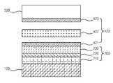
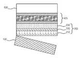
다음으로 공정 S2 및 S3에서는 도 5c와 도 5d에 도시된 바와 같이 화합물 반도체 구조물(200)위에 접착층(420)과 전도성 기판(500), 예를 들어 금속 기판 또는 Si 기판을 접합한다. 여기에서 접착층(420)은 전도성 기판(500)과 화합물 반도체 구조물(200)을 접합하는 역할을 하는 것으로, 도 5c에 도시된 바와 같이 제 1 솔더층(421), 발열층(422) 및 제 2 솔더층(423)이 독립된 층으로서 순차적으로 적층되어 이루어진다.Next, in steps S2 and S3, the
이와는 다르게, 도 5d에 도시된 바와 같이 화합물 반도체 구조물(200) 상에 제 1 솔더층(421)을 형성하고, 제 1 솔더층(421) 상에 발열층(422)을 형성한 뒤, 전도성 기판(500)의 제 1 면에 형성된 제 2 솔더층(423)을 적층하는 방식으로 이루어질 수 있다.Alternatively, as shown in FIG. 5D, the
다음으로 공정 S4 및 S5에서는 발열층(422)을 점화(ignition)시켜 전도성 기판(500)과 화합물 반도체 구조물(200)을 접합한다.Next, in steps S4 and S5, the heat generating
도 6은 도 4에 도시된 발열층(422) 일부의 일부 층만을 확대 도시한 종단면도로서, 예를 들어 알루미늄(Al) 박막(431)과 니켈(Ni) 박막(432)이 나노 두께로 교번 적층된 다중 박막 구조의 발열층(422)의 일부 층을 도시하고 있다. 도 6에 도시된 바와 같이 발열층(422)은 Al/Ni, Al/Ti, Ni/Si, Nb/Si 및 Al/Monel(Ni과 Cu의 7:3비율 합금) 조합들 중에서 어느 하나의 조합을 이루는 두 성분이 나노 두께로 수백 내지 수천 번 정도 교번 적층된 다중 박막 구조로 이루어질 수 있다. 전술한 다층 박막 구조는 예를 들어, 분리 가능한 포일 형태로 형성되거나 하부구조인 제 1 솔더층(421) 상에 직접 증착하여 형성할 수 있다. 이때, 하부구조 상에 직접 증착법으로 형성하는 경우에 인시츄(in-situ) 방식으로 실시하면 얼라이닝 공정 등을 생략할 수 있다.FIG. 6 is an enlarged longitudinal sectional view of only a part of a portion of the
또 다른 실시예로 발열층(422)은 상기한 조합을 이루는 두 성분이 조밀한 파우더 형태로 배합되어 이루어질 수도 있다.In another embodiment, the
도 7은 발열층(422)이 점화되고 반응이 전파되는 모습을 나타낸 종단면도이다. 도 7에 도시한 바와 같이, 발열층(422)을 점화하는 방식으로는 자전 연소 합성법(SHS: Self-propagating High-temperature Synthesis)이 사용될 수 있는데, 이에 따르면 전기적, 광학적 또는 열적 형태의 작은 에너지의 점화원이 발열층(422)에 국부적으로 주어지면 반응이 시작된다. 반응이 시작되면 이를 기화로 매우 짧은 시간동안 급격하게 온도가 오르고 많은 양의 에너지가 발생되게 되며, 이에 따라 반응이 스스로 전파(self-propagating)된다. 좀 더 구체적으로 설명하자면, 전술한 반응의 전파 속도는 레이어의 두께에 따라 달라질 수 있으나, 대략 30m/s 까지 상승할 수 있고, 반응에 의한 국부적인 열의 온도는 수천분의 1초 동안 1200℃를 넘어서까지 도달할 수 있다. 또한, 발열층(422)의 반응에 의해 발생되는 고온의 에너지가 제 1 솔더층(421)과 제 2 솔더층(423)에 전달될 때 정확하고 국부적으로 전달되어 분산되지 않는 특징이 있기 때문에 전도성 기판(500)과 사파이어 기판(100)은 열적 손상을 입지 않고, 상기 종래 기술에서 발생되었던 열팽창 계수에 따른 웨이퍼 휘어짐 현상이 일어나지 않게 된다. 더하여 이러한 공정 방법은 노(furnace)가 필요 없고, 외적인 열원을 따로 구비하지 않아도 되는 장점이 있다.7 is a longitudinal cross-sectional view showing the
도 7에는 점화가 시작되어 반응이 끝난 부분(441)과 에너지가 전파되어 반응이 진행 중인 부분(442) 및 아직 반응이 시작되지 않은 부분(443)이 도시되어 있다.7 shows a
도 8은 발열층에 의한 반응이 종결된 접착층(425)을 나타낸 종단면도이다. 전술한 발열층의 반응이 종결되면 접착층의 제 1 솔더층(421)과 제 2 솔더층(423)은 완전히 접착된 상태가 된다.8 is a longitudinal sectional view showing the
이후, 도 3의 공정 S6에서는 도 5e에 도시된 바와 같이 화합물 반도체 구조물(200)로부터 사파이어 기판(100)을 제거하는데, 이에 따라 전도성 기판(500) 상에 접착층(425)과 화합물 반도체 구조물(200)이 순차적으로 적층된 중간 제조물이 얻어진다. 이러한 중간 제조물 상에 도 4에 도시된 바와 같이 접촉 전극(600)을 형성하여 수직 LED를 제조할 수 있다.Subsequently, in step S6 of FIG. 3, as shown in FIG. 5E, the
본 발명의 수직 LED 제조 방법은 전술한 실시 예에 국한 되지 않고 본 발명의 기술 사상이 허용되는 범위에서 다양하게 변형하여 실시할 수가 있다.The method of manufacturing the vertical LED of the present invention is not limited to the above-described embodiment, and can be carried out in various modifications within the allowable technical spirit of the present invention.
100 : 사파이어 기판200 : 화합물 반도체 구조물
210 : n형 화합물 반도체층220 : 활성화층
230 : p형 화합물 반도체층420 : 접착층
421 : 제 1 솔더층422 : 발열층
423 : 제 2 솔더층425 : 접착층(반응 후)
500 : 전도성 기판600 : 접촉 전극100: sapphire substrate 200: compound semiconductor structure
210: n-type compound semiconductor layer 220: active layer
230: p-type compound semiconductor layer 420: adhesive layer
421: first solder layer 422: heat generating layer
423: second solder layer 425: adhesive layer (after reaction)
500
Claims (8)
Translated fromKorean상기 LED 화합물 반도체 구조물 위에 제 1 솔더층(421), 발열층(422) 및 제 2 솔더층(423)의 순서로 적층된 접착층(420)을 형성하는 공정;
상기 접착층 위에 전도성 기판을 형성하는 공정;
상기 발열층을 반응시켜 발생하는 열에 의해 제 1 솔더층(421)과 제 2 솔더층(423)을 접합하는 공정 및
상기 사파이어 기판을 제거하는 공정을 포함하여 이루어진 수직형 LED 제조 방법.Growing the LED compound semiconductor structure 200 on the sapphire substrate;
Forming an adhesive layer 420 stacked on the LED compound semiconductor structure in an order of a first solder layer 421, a heating layer 422, and a second solder layer 423;
Forming a conductive substrate on the adhesive layer;
Bonding the first solder layer 421 and the second solder layer 423 by heat generated by reacting the heat generating layer; and
Vertical LED manufacturing method comprising the step of removing the sapphire substrate.
상기 LED 화합물 반도체 구조물 위에 제1 솔더층(421)을 형성하는 공정;
상기 솔더층(421)상에 발열층(422)을 형성하는 공정;
전도성 기판의 제 1 면에 제2 솔더층(423)을 형성하는 공정;
상기 발열층을 반응시켜 발생하는 열에 의해 제 1 솔더층(421)과 제 2 솔더층(423)을 접합하는 공정 및
상기 사파이어 기판을 제거하는 공정을 포함하여 이루어진 수직형 LED 제조 방법.Growing the LED compound semiconductor structure 200 on the sapphire substrate;
Forming a first solder layer (421) on the LED compound semiconductor structure;
Forming a heating layer (422) on the solder layer (421);
Forming a second solder layer 423 on the first surface of the conductive substrate;
Bonding the first solder layer 421 and the second solder layer 423 by heat generated by reacting the heat generating layer; and
Vertical LED manufacturing method comprising the step of removing the sapphire substrate.
상기 발열층은 Al/Ni, Al/Ti, Ni/Si, Nb/Si 및 Al/Monel 조합들 중에서 어느 하나의 조합을 이루는 두 성분이 교번 적층된 다중 박막 구조의 포일 형태로 형성되는 것을 특징으로 하는 수직형 LED 제조 방법.The method according to claim 1 or 2,
The heating layer is formed in the form of a foil of a multi-layered structure in which two components constituting any combination of Al / Ni, Al / Ti, Ni / Si, Nb / Si, and Al / Monel combinations are alternately stacked. Vertical LED manufacturing method.
상기 발열층은 Al/Ni, Al/Ti, Ni/Si, Nb/Si 및 Al/Monel 조합들 중에서 어느 하나의 조합을 이루는 두 성분이 교번 적층된 다중 박막 구조를 상기 제 1 솔더층(421) 또는 제 2 솔더층(423)상에 직접 증착하여 형성되는 것을 특징으로 하는 수직형 LED 제조 방법.The method according to claim 1 or 2,
The heat generating layer has a multi-layered thin film structure in which two components forming one of Al / Ni, Al / Ti, Ni / Si, Nb / Si, and Al / Monel combinations are alternately stacked. Or the vertical LED manufacturing method characterized in that formed by depositing directly on the second solder layer (423).
상기 발열층은 Al/Ni, Al/Ti, Ni/Si, Nb/Si 및 Al/Monel 조합들 중에서 어느 하나의 조합을 이루는 두 성분이 교번 적층된 다중 박막 구조를 상기 화합물 반도체 구조물(200) 또는 전도성 기판(500)상에 직접 증착하여 형성되는 것을 특징으로 하는 수직형 LED 제조 방법.
The method according to claim 1 or 2,
The heating layer has a multi-layered thin film structure in which two components forming one of Al / Ni, Al / Ti, Ni / Si, Nb / Si, and Al / Monel combinations are alternately stacked. Vertical LED manufacturing method characterized in that formed by directly depositing on a conductive substrate (500).
상기 발열층은 Al/Ni, Al/Ti, Ni/Si, Nb/Si 및 Al/Monel 조합들 중에서 어느 하나의 조합을 이루는 두 성분이 파우더 형태로 배합되어 형성되는 것을 특징으로 하는 수직형 LED 제조 방법.The method according to claim 1 or 2,
The heat generating layer is a vertical LED manufacturing, characterized in that the combination of the two components forming any one of the combination of Al / Ni, Al / Ti, Ni / Si, Nb / Si and Al / Monel in powder form Way.
상기 발열층은 자전 연소 합성법(Self-propagating High-temperature Synthesis)에 의해 발열되는 것을 특징으로 하는 수직형 LED 제조 방법.The method according to claim 1 or 2,
The heating layer is a vertical LED manufacturing method characterized in that the heat generated by the self-propagating High-temperature Synthesis.
상기 발열층의 반응은 전기적, 광학적, 열적 에너지원에 의해 점화되는 것을 특징으로 하는 수직형 LED 제조 방법.The method according to claim 1 or 2,
The reaction of the heating layer is a vertical LED manufacturing method, characterized in that the ignition by an electrical, optical, thermal energy source.
Priority Applications (3)
| Application Number | Priority Date | Filing Date | Title |
|---|---|---|---|
| KR1020100115074AKR101035998B1 (en) | 2010-11-18 | 2010-11-18 | Vertical LED Manufacturing Method |
| US13/988,325US20130230937A1 (en) | 2010-11-18 | 2011-05-25 | Method for manufacturing perpendicular led |
| PCT/KR2011/003822WO2012067326A1 (en) | 2010-11-18 | 2011-05-25 | Method for manufacturing perpendicular led |
Applications Claiming Priority (1)
| Application Number | Priority Date | Filing Date | Title |
|---|---|---|---|
| KR1020100115074AKR101035998B1 (en) | 2010-11-18 | 2010-11-18 | Vertical LED Manufacturing Method |
Publications (1)
| Publication Number | Publication Date |
|---|---|
| KR101035998B1true KR101035998B1 (en) | 2011-05-23 |
Family
ID=44366358
Family Applications (1)
| Application Number | Title | Priority Date | Filing Date |
|---|---|---|---|
| KR1020100115074AExpired - Fee RelatedKR101035998B1 (en) | 2010-11-18 | 2010-11-18 | Vertical LED Manufacturing Method |
Country Status (3)
| Country | Link |
|---|---|
| US (1) | US20130230937A1 (en) |
| KR (1) | KR101035998B1 (en) |
| WO (1) | WO2012067326A1 (en) |
Cited By (1)
| Publication number | Priority date | Publication date | Assignee | Title |
|---|---|---|---|---|
| KR20240027469A (en) | 2022-08-23 | 2024-03-04 | 한국광기술원 | Manufacturing method of micro vertical led display |
Families Citing this family (1)
| Publication number | Priority date | Publication date | Assignee | Title |
|---|---|---|---|---|
| US9324566B1 (en) | 2014-12-31 | 2016-04-26 | International Business Machines Corporation | Controlled spalling using a reactive material stack |
Citations (4)
| Publication number | Priority date | Publication date | Assignee | Title |
|---|---|---|---|---|
| KR20040005612A (en)* | 2002-07-08 | 2004-01-16 | 니치아 카가쿠 고교 가부시키가이샤 | Method of Manufacturing Nitride Semiconductor Device and Nitride Semiconductor Device |
| KR100632004B1 (en) | 2005-08-12 | 2006-10-09 | 삼성전기주식회사 | Nitride single crystal substrate manufacturing method and nitride semiconductor light emitting device manufacturing method |
| JP2009016748A (en) | 2007-07-09 | 2009-01-22 | Toshiba Discrete Technology Kk | Semiconductor light emitting device and manufacturing method thereof |
| KR20100109169A (en)* | 2009-03-31 | 2010-10-08 | 서울옵토디바이스주식회사 | Fabrication method of light emitting diode and the light emitting diode fabricated by the method |
Family Cites Families (4)
| Publication number | Priority date | Publication date | Assignee | Title |
|---|---|---|---|---|
| US5381944A (en)* | 1993-11-04 | 1995-01-17 | The Regents Of The University Of California | Low temperature reactive bonding |
| US6736942B2 (en)* | 2000-05-02 | 2004-05-18 | Johns Hopkins University | Freestanding reactive multilayer foils |
| KR100835076B1 (en)* | 2006-12-08 | 2008-06-03 | 삼성전기주식회사 | Vertical structure LED device and manufacturing method thereof |
| US8207547B2 (en)* | 2009-06-10 | 2012-06-26 | Brudgelux, Inc. | Thin-film LED with P and N contacts electrically isolated from the substrate |
- 2010
- 2010-11-18KRKR1020100115074Apatent/KR101035998B1/ennot_activeExpired - Fee Related
- 2011
- 2011-05-25USUS13/988,325patent/US20130230937A1/ennot_activeAbandoned
- 2011-05-25WOPCT/KR2011/003822patent/WO2012067326A1/enactiveApplication Filing
Patent Citations (4)
| Publication number | Priority date | Publication date | Assignee | Title |
|---|---|---|---|---|
| KR20040005612A (en)* | 2002-07-08 | 2004-01-16 | 니치아 카가쿠 고교 가부시키가이샤 | Method of Manufacturing Nitride Semiconductor Device and Nitride Semiconductor Device |
| KR100632004B1 (en) | 2005-08-12 | 2006-10-09 | 삼성전기주식회사 | Nitride single crystal substrate manufacturing method and nitride semiconductor light emitting device manufacturing method |
| JP2009016748A (en) | 2007-07-09 | 2009-01-22 | Toshiba Discrete Technology Kk | Semiconductor light emitting device and manufacturing method thereof |
| KR20100109169A (en)* | 2009-03-31 | 2010-10-08 | 서울옵토디바이스주식회사 | Fabrication method of light emitting diode and the light emitting diode fabricated by the method |
Cited By (1)
| Publication number | Priority date | Publication date | Assignee | Title |
|---|---|---|---|---|
| KR20240027469A (en) | 2022-08-23 | 2024-03-04 | 한국광기술원 | Manufacturing method of micro vertical led display |
Also Published As
| Publication number | Publication date |
|---|---|
| WO2012067326A1 (en) | 2012-05-24 |
| US20130230937A1 (en) | 2013-09-05 |
Similar Documents
| Publication | Publication Date | Title |
|---|---|---|
| US7724791B2 (en) | Method of manufacturing laser diode packages and arrays | |
| JP4852755B2 (en) | Method for manufacturing compound semiconductor device | |
| CN101740694B (en) | Light emitting device and method of fabricating light emitting device | |
| TW201031027A (en) | Method for manufacturing light emitting device | |
| TWI540772B (en) | LED light-emitting element holding substrate for substrate and manufacturing method thereof | |
| JP2014525674A (en) | Semiconductor structure processing method | |
| JP2014529908A (en) | Discontinuous patterned bonding and related systems and methods for semiconductor devices | |
| TW201126693A (en) | Top view type of light emitting diode package structure and fabrication thereof | |
| KR101148028B1 (en) | Method for manufacturing heat dissipation bulk of semiconductor device | |
| JP2009176961A (en) | Method of manufacturing mounting substrate, and method of manufacturing linear light source | |
| TW201448274A (en) | Semiconductor light emitting device, light emitting device, and method of manufacturing semiconductor light emitting device | |
| KR101035998B1 (en) | Vertical LED Manufacturing Method | |
| KR20080047838A (en) | Vertical structure nitride semiconductor light emitting device and manufacturing method | |
| JP2006049736A (en) | Thermoelectric module | |
| CN107924828B (en) | Electronic device and method for manufacturing electronic device | |
| KR20110065202A (en) | Apparatus and manufacturing method of LED element having conductive substrate as carrier | |
| TWI467808B (en) | Light-emitting diode element, manufacturing method thereof and light-emitting device | |
| KR101499954B1 (en) | fabrication of vertical structured light emitting diodes using group 3 nitride-based semiconductors and its related methods | |
| KR101210426B1 (en) | Sub-mount substrate for semiconductor light emitting element and method of fabricating a semiconductor light emitting element using the same | |
| JP2009277852A (en) | Semiconductor light-emitting element and method of manufacturing the same | |
| CN114171659A (en) | Deep ultraviolet thin film LED with high light extraction efficiency and preparation method thereof | |
| TWI618264B (en) | Photoelectric element and method of manufacturing same | |
| TWI513057B (en) | Wavelength converter for solid state lighting devices, and related systems and methods | |
| KR101526566B1 (en) | fabrication of vertical structured light emitting diodes using group 3 nitride-based semiconductors and its related methods | |
| CN107709272A (en) | Method for connecting at least two parts |
Legal Events
| Date | Code | Title | Description |
|---|---|---|---|
| PA0109 | Patent application | St.27 status event code:A-0-1-A10-A12-nap-PA0109 | |
| A201 | Request for examination | ||
| A302 | Request for accelerated examination | ||
| PA0201 | Request for examination | St.27 status event code:A-1-2-D10-D11-exm-PA0201 | |
| PA0302 | Request for accelerated examination | St.27 status event code:A-1-2-D10-D17-exm-PA0302 St.27 status event code:A-1-2-D10-D16-exm-PA0302 | |
| D13-X000 | Search requested | St.27 status event code:A-1-2-D10-D13-srh-X000 | |
| D14-X000 | Search report completed | St.27 status event code:A-1-2-D10-D14-srh-X000 | |
| E701 | Decision to grant or registration of patent right | ||
| PE0701 | Decision of registration | St.27 status event code:A-1-2-D10-D22-exm-PE0701 | |
| GRNT | Written decision to grant | ||
| PR0701 | Registration of establishment | St.27 status event code:A-2-4-F10-F11-exm-PR0701 | |
| PR1002 | Payment of registration fee | St.27 status event code:A-2-2-U10-U11-oth-PR1002 Fee payment year number:1 | |
| PG1601 | Publication of registration | St.27 status event code:A-4-4-Q10-Q13-nap-PG1601 | |
| FPAY | Annual fee payment | Payment date:20140514 Year of fee payment:4 | |
| PR1001 | Payment of annual fee | St.27 status event code:A-4-4-U10-U11-oth-PR1001 Fee payment year number:4 | |
| FPAY | Annual fee payment | Payment date:20150508 Year of fee payment:5 | |
| PR1001 | Payment of annual fee | St.27 status event code:A-4-4-U10-U11-oth-PR1001 Fee payment year number:5 | |
| LAPS | Lapse due to unpaid annual fee | ||
| PC1903 | Unpaid annual fee | St.27 status event code:A-4-4-U10-U13-oth-PC1903 Not in force date:20160514 Payment event data comment text:Termination Category : DEFAULT_OF_REGISTRATION_FEE | |
| PC1903 | Unpaid annual fee | St.27 status event code:N-4-6-H10-H13-oth-PC1903 Ip right cessation event data comment text:Termination Category : DEFAULT_OF_REGISTRATION_FEE Not in force date:20160514 | |
| P22-X000 | Classification modified | St.27 status event code:A-4-4-P10-P22-nap-X000 |