KR101035054B1 - Tag Antenna and its manufacturing method - Google Patents
Tag Antenna and its manufacturing methodDownload PDFInfo
- Publication number
- KR101035054B1 KR101035054B1KR1020080133871AKR20080133871AKR101035054B1KR 101035054 B1KR101035054 B1KR 101035054B1KR 1020080133871 AKR1020080133871 AKR 1020080133871AKR 20080133871 AKR20080133871 AKR 20080133871AKR 101035054 B1KR101035054 B1KR 101035054B1
- Authority
- KR
- South Korea
- Prior art keywords
- dielectric
- tag antenna
- radiator
- chip
- ground
- Prior art date
- Legal status (The legal status is an assumption and is not a legal conclusion. Google has not performed a legal analysis and makes no representation as to the accuracy of the status listed.)
- Active
Links
- 238000004519manufacturing processMethods0.000titleclaimsabstractdescription23
- 238000000034methodMethods0.000claimsabstractdescription13
- 239000011248coating agentSubstances0.000claimsdescription19
- 238000000576coating methodMethods0.000claimsdescription19
- 239000004020conductorSubstances0.000claimsdescription18
- 239000000463materialSubstances0.000claimsdescription15
- 239000003989dielectric materialSubstances0.000claimsdescription14
- 230000000149penetrating effectEffects0.000claimsdescription3
- 238000005530etchingMethods0.000claimsdescription2
- 239000007788liquidSubstances0.000abstractdescription7
- 239000002184metalSubstances0.000abstractdescription7
- 230000002950deficientEffects0.000abstract1
- 238000010586diagramMethods0.000description6
- 230000005611electricityEffects0.000description4
- 230000035939shockEffects0.000description4
- 230000003068static effectEffects0.000description4
- 230000007257malfunctionEffects0.000description3
- 238000010030laminatingMethods0.000description2
- 230000005856abnormalityEffects0.000description1
- 230000005540biological transmissionEffects0.000description1
- 230000007547defectEffects0.000description1
- 238000003475laminationMethods0.000description1
Images


Classifications
- H—ELECTRICITY
- H01—ELECTRIC ELEMENTS
- H01Q—ANTENNAS, i.e. RADIO AERIALS
- H01Q1/00—Details of, or arrangements associated with, antennas
- H01Q1/40—Radiating elements coated with or embedded in protective material
- H—ELECTRICITY
- H01—ELECTRIC ELEMENTS
- H01Q—ANTENNAS, i.e. RADIO AERIALS
- H01Q1/00—Details of, or arrangements associated with, antennas
- H01Q1/12—Supports; Mounting means
- H01Q1/22—Supports; Mounting means by structural association with other equipment or articles
- H01Q1/2208—Supports; Mounting means by structural association with other equipment or articles associated with components used in interrogation type services, i.e. in systems for information exchange between an interrogator/reader and a tag/transponder, e.g. in Radio Frequency Identification [RFID] systems
- H01Q1/2225—Supports; Mounting means by structural association with other equipment or articles associated with components used in interrogation type services, i.e. in systems for information exchange between an interrogator/reader and a tag/transponder, e.g. in Radio Frequency Identification [RFID] systems used in active tags, i.e. provided with its own power source or in passive tags, i.e. deriving power from RF signal
- H—ELECTRICITY
- H01—ELECTRIC ELEMENTS
- H01Q—ANTENNAS, i.e. RADIO AERIALS
- H01Q1/00—Details of, or arrangements associated with, antennas
- H01Q1/36—Structural form of radiating elements, e.g. cone, spiral, umbrella; Particular materials used therewith
- H01Q1/38—Structural form of radiating elements, e.g. cone, spiral, umbrella; Particular materials used therewith formed by a conductive layer on an insulating support
- H—ELECTRICITY
- H01—ELECTRIC ELEMENTS
- H01Q—ANTENNAS, i.e. RADIO AERIALS
- H01Q1/00—Details of, or arrangements associated with, antennas
- H01Q1/42—Housings not intimately mechanically associated with radiating elements, e.g. radome
- H01Q1/422—Housings not intimately mechanically associated with radiating elements, e.g. radome comprising two or more layers of dielectric material
- H—ELECTRICITY
- H01—ELECTRIC ELEMENTS
- H01Q—ANTENNAS, i.e. RADIO AERIALS
- H01Q23/00—Antennas with active circuits or circuit elements integrated within them or attached to them
- H—ELECTRICITY
- H01—ELECTRIC ELEMENTS
- H01Q—ANTENNAS, i.e. RADIO AERIALS
- H01Q1/00—Details of, or arrangements associated with, antennas
- H01Q1/002—Protection against seismic waves, thermal radiation or other disturbances, e.g. nuclear explosion; Arrangements for improving the power handling capability of an antenna
- Y—GENERAL TAGGING OF NEW TECHNOLOGICAL DEVELOPMENTS; GENERAL TAGGING OF CROSS-SECTIONAL TECHNOLOGIES SPANNING OVER SEVERAL SECTIONS OF THE IPC; TECHNICAL SUBJECTS COVERED BY FORMER USPC CROSS-REFERENCE ART COLLECTIONS [XRACs] AND DIGESTS
- Y10—TECHNICAL SUBJECTS COVERED BY FORMER USPC
- Y10T—TECHNICAL SUBJECTS COVERED BY FORMER US CLASSIFICATION
- Y10T29/00—Metal working
- Y10T29/49—Method of mechanical manufacture
- Y10T29/49002—Electrical device making
- Y10T29/49016—Antenna or wave energy "plumbing" making
- Y10T29/49018—Antenna or wave energy "plumbing" making with other electrical component
Landscapes
- Details Of Aerials (AREA)
Abstract
Translated fromKoreanDescription
Translated fromKorean본 발명은 태그 안테나 및 그 제조방법에 관한 것으로, 특히, 칩이 유전체의 내부에 위치한 태그 안테나 및 그 제조방법에 관한 것이다.The present invention relates to a tag antenna and a method of manufacturing the same, and more particularly, to a tag antenna and a method of manufacturing the tag is located inside the dielectric.
RFID(Radio Frequency Identification)는 전파 신호를 통해 비접촉식으로 사물에 부착된 얇은 평면 형태의 태그를 식별하여 정보를 처리하는 시스템을 의미하며, 이를 이용한 태그 안테나는 현재 물류, 교통, 보안, 안전 등의 다양한 응용 분야에 활용되고 있다.RFID (Radio Frequency Identification) refers to a system that processes information by identifying a thin flat tag attached to an object in a non-contact manner through a radio signal, and the tag antenna using it is currently used in various fields such as logistics, traffic, security, and safety. It is used for application fields.
도 1은 종래 태그 안테나의 구성도로서, 도 1을 참조하면, 기존의 태그 안테나는 유전체(11), 방사체(13), 그라운드(15), 접지선(17) 및 태그 칩(19)을 포함한다. 그런데, 이러한 기존의 태그 안테나는 도 1과 같이 칩(19)이 돌출된 형태를 갖고 있다. 따라서 외부 충격, 정전기, 온도, 압력, 습도 등에 민감하게 되어 불량률이 높았으며, 실제 사용시 인식률을 저하되었다.1 is a block diagram of a conventional tag antenna. Referring to FIG. 1, a conventional tag antenna includes a dielectric 11, a
이로 인해, 실제 사용 전에 태그 안테나의 상태를 일일이 확인하여 이상 여부를 확인해야 하는 번거로움이 있었으며, 금속이나 액체의 내부에 위치하는 등 특 수한 용도에서의 사용이 제한되는 문제가 있었다.For this reason, there is a hassle to check the state of the tag antenna to check whether the abnormality before the actual use, and there is a problem that the use in a special use, such as being located inside the metal or liquid.
본 발명은 상기한 종래의 문제점을 해결하기 위해 제안된 것으로서, 태그 칩을 유전체 내부에 위치하도록 하여 외부 환경에 강하고 금속이나 액체 등의 내부에 위치하는 등 특수 목적에 사용될 수 있는 태그 안테나 및 그 제조방법을 제공하는데 그 목적이 있다.The present invention has been proposed to solve the above-mentioned conventional problems, the tag antenna to be placed inside the dielectric, strong to the external environment and can be used for special purposes, such as a metal or a liquid and the like, and its manufacture The purpose is to provide a method.
상기와 같은 목적을 달성하기 위한 본 발명의 태그 안테나는, 제1 유전체와 상기 제1 유전체 위에 적층된 제2 유전체로 이루어진 유전체 층, 상기 유전체 층의 상면에 위치한 방사체, 상기 유전체 층의 하면에 위치한 그라운드, 상기 방사체 및 그라운드를 연결하는 접지선, 상기 제2 유전체의 내부에 위치한 칩(chip), 및 상기 칩의 다리와 상기 방사체를 연결하는 비아(via) 홀을 포함한다.The tag antenna of the present invention for achieving the above object, a dielectric layer consisting of a first dielectric and a second dielectric stacked on the first dielectric, a radiator located on the upper surface of the dielectric layer, a lower surface of the dielectric layer A ground, a ground line connecting the radiator and the ground, a chip positioned inside the second dielectric, and a via hole connecting the leg of the chip and the radiator.
본 발명의 태그 안테나에 있어서, 상기 제1 유전체 및 제2 유전체는, 동일한 물질로 이루어진 것을 특징으로 한다.In the tag antenna of the present invention, the first dielectric material and the second dielectric material are made of the same material.
본 발명의 태그 안테나에 있어서, 상기 제1 유전체 및 제2 유전체는, 서로 다른 물질로 이루어진 것을 특징으로 한다.In the tag antenna of the present invention, the first dielectric material and the second dielectric material are made of different materials.
본 발명의 태그 안테나에 있어서, 상기 비아 홀은, 도체가 인쇄된 것을 특징으로 한다.In the tag antenna of the present invention, the via hole is characterized in that a conductor is printed.
본 발명의 태그 안테나에 있어서, 상기 비아 홀은, 도체가 충진된 것을 특징으로 한다.In the tag antenna of the present invention, the via hole is filled with a conductor.
상기와 같은 목적을 달성하기 위한 본 발명의 태그 안테나는, 제1 유전체와 상기 제1 유전체 위에 적층된 제2 유전체 및 상기 제2 유전체 사이에 위치하며 상기 제1 유전체 위에 적층된 제3 유전체로 이루어진 유전체 층, 상기 유전체 층의 상면에 위치한 방사체, 상기 유전체 층의 하면에 위치한 그라운드, 상기 방사체 및 그라운드를 연결하는 접지선, 상기 제3 유전체의 내부에 위치한 칩(chip), 및 상기 칩과 상기 방사체를 연결하는 연결선을 포함한다.The tag antenna of the present invention for achieving the above object is composed of a first dielectric, a second dielectric stacked on the first dielectric and a third dielectric positioned between the second dielectric and stacked on the first dielectric. A dielectric layer, a radiator located on an upper surface of the dielectric layer, a ground located on a bottom surface of the dielectric layer, a ground line connecting the radiator and the ground, a chip located inside the third dielectric, and a chip and the radiator It includes a connecting line to connect.
본 발명의 태그 안테나에 있어서, 상기 제1 유전체, 상기 제2 유전체 및 상기 제3 유전체 중 하나 이상의 유전체는, 서로 다른 물질로 이루어진 것을 특징으로 한다.In the tag antenna of the present invention, at least one of the first dielectric material, the second dielectric material, and the third dielectric material is made of different materials.
상기와 같은 목적을 달성하기 위한 본 발명의 태그 안테나 제조방법은, 도체로 이루어진 그라운드의 상면에 제1 유전체를 도포하는 제1 도포단계, 상기 제1 유전체의 상면에 칩을 적층하는 적층단계, 상기 칩이 적층된 제1 유전체의 상면에 제2 유전체를 도포하는 제2 도포단계, 상기 제2 유전체의 상면에 방사체를 도포하는 제3 도포단계, 및 상기 제1 유전체 및 상기 제2 유전체를 관통하여 상기 방사체와 상기 그라운드를 연결하는 접지선을 형성하고, 상기 제2 유전체를 관통하여 상기 방사체와 상기 칩의 다리를 연결하는 비아 홀을 형성하는 형성단계를 포함한다.The tag antenna manufacturing method of the present invention for achieving the above object, the first coating step of applying a first dielectric on the upper surface of the ground made of a conductor, the lamination step of laminating a chip on the upper surface of the first dielectric, A second coating step of applying a second dielectric to an upper surface of the first dielectric in which chips are stacked, a third coating step of applying a radiator to an upper surface of the second dielectric, and penetrating the first dielectric and the second dielectric And forming a ground line connecting the radiator and the ground, and forming a via hole connecting the radiator and the leg of the chip through the second dielectric.
본 발명의 태그 안테나 제조방법에 있어서, 상기 제1 유전체 및 상기 제2 유전체는, 동일한 물질로 이루어진 것을 특징으로 한다.In the method of manufacturing a tag antenna of the present invention, the first dielectric material and the second dielectric material are made of the same material.
본 발명의 태그 안테나 제조방법에 있어서, 상기 제1 유전체 및 상기 제2 유전체는, 서로 다른 물질로 이루어진 것을 특징으로 한다.In the method of manufacturing a tag antenna of the present invention, the first dielectric material and the second dielectric material are made of different materials.
본 발명의 태그 안테나 제조방법에 있어서, 상기 형성단계는, 도체를 인쇄하여 상기 방사체와 상기 칩의 다리를 연결하는 것을 특징으로 한다.In the tag antenna manufacturing method of the present invention, the forming step, characterized in that for connecting the bridge of the chip and the radiator by printing a conductor.
본 발명의 태그 안테나 제조방법에 있어서, 상기 형성단계는, 도체를 충진하여 상기 방사체와 상기 칩의 다리를 연결하는 것을 특징으로 한다.In the method of manufacturing a tag antenna of the present invention, the forming step is characterized by connecting the radiator and the bridge of the chip by filling the conductor.
상기와 같은 목적을 달성하기 위한 본 발명의 태그 안테나 제조방법은, 도체로 이루어진 그라운드의 상면에 제1 유전체를 도포하는 제1 도포단계, 상기 제1 유전체의 상면에 제2 유전체를 도포하는 제2 도포단계, 상기 제2 유전체의 중앙을 식각하고 식각된 부분에 칩을 적층하는 적층단계, 상기 칩의 연결선과 연결되도록 제2 유전체의 상면에 방사체를 도포하는 제3 도포단계, 상기 칩이 적층된 부분에 제3 유전체를 도포하는 제4 도포단계, 및 상기 제1 유전체 및 상기 제2 유전체를 관통하여 상기 방사체와 상기 그라운드를 연결하는 접지선을 형성하는 형성단계를 포함한다.In the tag antenna manufacturing method of the present invention for achieving the above object, a first coating step of applying a first dielectric on the upper surface of the ground made of a conductor, a second coating the second dielectric on the upper surface of the first dielectric A laminating step of etching the center of the second dielectric and stacking the chip on the etched portion, a third coating step of applying a radiator to the upper surface of the second dielectric so as to be connected to the connection line of the chip, and the chip And a fourth coating step of applying a third dielectric to the portion, and forming a ground line through the first dielectric and the second dielectric to connect the radiator and the ground.
본 발명의 태그 안테나 제조방법에 있어서, 상기 제1 유전체, 상기 제2 유전체 및 상기 제3 유전체 중 하나 이상의 유전체는, 서로 다른 물질로 이루어진 것을 특징으로 한다.In the method of manufacturing a tag antenna of the present invention, at least one of the first dielectric, the second dielectric, and the third dielectric is made of different materials.
본 발명에 의하면, 충격, 정전기, 온도, 압력, 습도 등의 외부 환경에 강한 태그 안테나를 제조할 수 있고, 안테나의 기능 이상 및 불량률을 최소화할 수 있으며, 금속 또는 액체 내부에 위치하는 등 특수한 용도에도 태그 안테나를 사용할 수 있다.According to the present invention, it is possible to manufacture a tag antenna that is resistant to external environments such as shock, static electricity, temperature, pressure, and humidity, and to minimize the malfunction and failure rate of the antenna, and to place it in a metal or a liquid. The tag antenna can also be used.
이하 첨부된 도면을 참조하여 본 발명이 속하는 기술분야에서 통상의 지식을 가진 자가 본 발명을 용이하게 실시할 수 있는 바람직한 실시예를 상세히 설명한다. 다만, 본 발명의 바람직한 실시예에 대한 동작 원리를 상세하게 설명함에 있어 관련된 공지 기능 또는 구성에 대한 구체적인 설명이 본 발명의 요지를 불필요하게 흐릴 수 있다고 판단되는 경우에는 그 상세한 설명을 생략한다. 또한, 도면 전체에 걸쳐 유사한 기능 및 작용을 하는 부분에 대해서는 동일한 도면 부호를 사용한다.Hereinafter, exemplary embodiments of the present invention will be described in detail with reference to the accompanying drawings. However, in describing in detail the operating principle of the preferred embodiment of the present invention, if it is determined that the detailed description of the related known functions or configurations may unnecessarily obscure the subject matter of the present invention, the detailed description thereof will be omitted. In addition, the same reference numerals are used for parts having similar functions and functions throughout the drawings.
도 2는 본 발명의 일 실시예에 따른 태그 안테나의 구성도이다. 도 2를 참조하면, 본 실시예에 따른 태그 안테나는 제1 유전체(21), 제2 유전체(23), 방사체(25), 그라운드(27), 접지선(29), 칩(31) 및 비아(via) 홀(33)을 포함한다.2 is a block diagram of a tag antenna according to an embodiment of the present invention. 2, the tag antenna according to the present embodiment includes a first dielectric 21, a second dielectric 23, a
제2 유전체(23)는 제1 유전체(21) 위에 적층되어 있고, 제2 유전체(23)의 상면에는 방사체(25)가 위치하며, 제1 유전체(21)의 하면에는 그라운드(ground)(27)가 위치한다. 이때, 제1 유전체(21)와 제2 유전체(23)는 예를 들어, 동일한 물질로 이루어질 수 있으며, 서로 다른 물질로 이루어질 수도 있다.The second dielectric 23 is stacked on the first dielectric 21, the
방사체(25)와 그라운드(27)는 제1 유전체(21)와 제2 유전체(23)를 관통하는 접지선(29)로 연결되어 있다.The
칩(31)은 무선 송수신을 위한 태그 칩으로서 제2 유전체(23)의 내부에 위치한다. 그리고 칩(31)의 다리는 제2 유전체(23)를 관통하는 비아 홀(33)을 통해 방사체(25)와 연결되어 있다.The
이를 통해, 칩(31)은 외부 충격이나, 정전기, 온도, 압력, 습도 등에 영향을 받지 않게 된다. 그리고 본 발명의 태그 안테나는, 금속이나 액체 내부에 위치하여서도 기능 이상 없이 태그 안테나로서 동작하는 것이 가능하다.As a result, the
비아 홀(33)은 방사체(25)와 칩(31)의 다리를 연결하기 위하여, 예를 들어, 홀에 도체가 인쇄된 형태로 이루어질 수 있으며, 비아 홀에 도체가 충진된 형태로 이루어질 수도 있다.The
도 3은 본 발명의 다른 일 실시예에 따른 태그 안테나의 구성도이다. 도 3을 참조하면, 본 실시예에 따른 태그 안테나는 제1 유전체(21), 제2 유전체(23), 제3 유전체(24), 방사체(25), 그라운드(27), 접지선(29), 칩(31) 및 연결선(35)을 포함한다.3 is a block diagram of a tag antenna according to another embodiment of the present invention. Referring to FIG. 3, the tag antenna according to the present exemplary embodiment includes a first dielectric 21, a second dielectric 23, a third dielectric 24, a
본 실시예에서 방사체(25)와 칩(31)은 연결선(35)으로 연결되어 있다. 그리고 제2 유전체(23) 사이에는 칩(31)과 연결선(35)을 둘러싼 제3 유전체(24)가 위치한다.In this embodiment, the
이때, 제1 유전체(21), 제2 유전체(23) 및 제3 유전체(24) 중 하나 이상의 유전체는, 예를 들어, 서로 다른 물질로 이루어질 수 있다.In this case, at least one of the first dielectric 21, the second dielectric 23, and the third dielectric 24 may be formed of, for example, different materials.
이를 통해, 칩(31)은 외부 충격이나, 정전기, 온도, 압력, 습도 등에 영향을 받지 않게 되고, 본 실시예의 태그 안테나가 금속이나 액체 내부에 위치하여서도 기능 이상 없이 태그 안테나로서 동작하는 것이 가능한 점은 상기한 바와 같다.As a result, the
본 발명의 일 실시예에 따른 태그 안테나 제조방법에 대해서는 도 4 및 도 5를 참조하여 좀 더 상세하게 설명하기로 한다.A method of manufacturing a tag antenna according to an embodiment of the present invention will be described in more detail with reference to FIGS. 4 and 5.
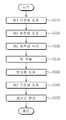
도 4는 본 발명의 일 실시예에 따른 태그 안테나 제조방법의 흐름도이다. 도 4를 참조하면, 도체로 이루어진 그라운드(27)의 상면에 제1 유전체(21)를 도포한다(S410). 그리고 단계(S410)에서 적층한 제1 유전체(21)의 상면에 칩(31)을 적층하고(S420), 칩(31)을 둘러싸도록 제1 유전체(21)의 상면에 제2 유전체(23)을 도포한다(S430).4 is a flowchart illustrating a tag antenna manufacturing method according to an embodiment of the present invention. Referring to FIG. 4, the first dielectric 21 is coated on the upper surface of the
제2 유전체(23)의 상면에는 방사체(25)를 도포하고(S440), 방사체(25)와 그라운드(27)를 연결하도록 제1 유전체(21)와 제2 유전체(23)를 광통하는 접지선(29)을 형성한다(S450). 그리고, 제2 유전체(23)를 관통하여 방사체(25)와 칩(31)의 다리를 연결하는 비아 홀(33)을 형성한다(S460).The
단계(S450) 및 단계(S460)은 서로 순서를 바꾸어 이루어질 수 있다. 단계(S460)에서 형성된 비아 홀(33)은, 예를 들어, 그 내부에 도체가 인쇄되거나, 도체로 충진된다.Steps S450 and S460 may be performed in a reverse order. In the
도 5는 본 발명의 다른 일 실시예에 따른 태그 안테나 제조방법의 흐름도이다. 도 5를 참조하면, 도체로 이루어진 그라운드(27)의 상면에 제1 유전체(21)를 도포하고(S510), 제1 유전체(21)의 상면에 제2 유전체(23)를 도포한다(S520).5 is a flowchart illustrating a tag antenna manufacturing method according to another embodiment of the present invention. Referring to FIG. 5, a first dielectric 21 is coated on an upper surface of a
이후, 단계(S520)에서 도포한 제2 유전체(23)의 중앙을 식각하고(S530), 단계(S530)에서 식각된 부분에 칩(31)을 적층한다(S540).Thereafter, the center of the second dielectric 23 applied in step S520 is etched (S530), and the
그리고 칩(31)의 연결선과 연결되도록 제2 유전체(23)의 상면에 방사체(25)를 도포하고(S550), 단계(S530)에서 식각하고 단계(S540)에서 칩(31)을 적층한 부분에 제3유전체를 도포한다(S560).In addition, the
방사체(25)와 그라운드(27)는 제1 유전체(21) 및 제2 유전체(23)를 관통하는 접지선을 형성하여 연결한다(S570). 단계(S570)는 단계(S560)와 순서를 바꾸어 이루어질 수도 있다.The
본 발명의 태그 안테나는 태그 칩이 유전체의 내부에 위치하도록 하여, 외부 환경에 따른 영향을 덜 받도록 설계되었다. 본 발명의 태그 안테나는 물류, 교통, 보안, 안전 등 다양한 분야에서 활용될 수 있으며, 특히 태그 안테나가 금속이나 액체 내부에 위치한 형태로 사용할 수도 있다.The tag antenna of the present invention is designed so that the tag chip is located inside the dielectric, so that it is less affected by the external environment. The tag antenna of the present invention may be utilized in various fields such as logistics, traffic, security, and safety, and in particular, the tag antenna may be used in the form of a metal or a liquid.
도 1은 종래의 태그 안테나의 구성도이다.1 is a block diagram of a conventional tag antenna.
도 2은 본 발명의 일 실시예에 따른 태그 안테나의 구성도이다.2 is a block diagram of a tag antenna according to an embodiment of the present invention.
도 3은 본 발명의 다른 일 실시예에 따른 태그 안테나의 구성도이다.3 is a block diagram of a tag antenna according to another embodiment of the present invention.
도 4는 본 발명의 일 실시예에 따른 태그 안테나 제조방법의 흐름도이다.4 is a flowchart illustrating a tag antenna manufacturing method according to an embodiment of the present invention.
도 5는 본 발명의 다른 일 실시예에 따른 태그 안테나 제조방법의 흐름도이다.5 is a flowchart illustrating a tag antenna manufacturing method according to another embodiment of the present invention.
Claims (14)
Translated fromKoreanPriority Applications (2)
| Application Number | Priority Date | Filing Date | Title |
|---|---|---|---|
| KR1020080133871AKR101035054B1 (en) | 2008-12-24 | 2008-12-24 | Tag Antenna and its manufacturing method |
| US12/655,058US8350760B2 (en) | 2008-12-24 | 2009-12-21 | Antenna using buildup structure and method of manufacturing the same |
Applications Claiming Priority (1)
| Application Number | Priority Date | Filing Date | Title |
|---|---|---|---|
| KR1020080133871AKR101035054B1 (en) | 2008-12-24 | 2008-12-24 | Tag Antenna and its manufacturing method |
Publications (2)
| Publication Number | Publication Date |
|---|---|
| KR20100075231A KR20100075231A (en) | 2010-07-02 |
| KR101035054B1true KR101035054B1 (en) | 2011-05-19 |
Family
ID=42265242
Family Applications (1)
| Application Number | Title | Priority Date | Filing Date |
|---|---|---|---|
| KR1020080133871AActiveKR101035054B1 (en) | 2008-12-24 | 2008-12-24 | Tag Antenna and its manufacturing method |
Country Status (2)
| Country | Link |
|---|---|
| US (1) | US8350760B2 (en) |
| KR (1) | KR101035054B1 (en) |
Citations (4)
| Publication number | Priority date | Publication date | Assignee | Title |
|---|---|---|---|---|
| JP2002535758A (en) | 1999-01-13 | 2002-10-22 | ブレイディー ワールドワイド インコーポレイテッド | Laminated RFID label and method of manufacturing the same |
| JP2006018501A (en) | 2004-06-30 | 2006-01-19 | Sagawa Insatsu Kk | Ic tag for physical distribution |
| JP2008009514A (en) | 2006-06-27 | 2008-01-17 | Mitsubishi Electric Corp | RFID tag and manufacturing method thereof |
| KR20080021354A (en)* | 2006-09-04 | 2008-03-07 | 주식회사 부광실업 | How to manufacture a contactless card |
Family Cites Families (11)
| Publication number | Priority date | Publication date | Assignee | Title |
|---|---|---|---|---|
| FR2673041A1 (en)* | 1991-02-19 | 1992-08-21 | Gemplus Card Int | METHOD FOR MANUFACTURING INTEGRATED CIRCUIT MICROMODULES AND CORRESPONDING MICROMODULE. |
| US7158031B2 (en)* | 1992-08-12 | 2007-01-02 | Micron Technology, Inc. | Thin, flexible, RFID label and system for use |
| US7002475B2 (en)* | 1997-12-31 | 2006-02-21 | Intermec Ip Corp. | Combination radio frequency identification transponder (RFID tag) and magnetic electronic article surveillance (EAS) tag |
| US6509217B1 (en)* | 1999-10-22 | 2003-01-21 | Damoder Reddy | Inexpensive, reliable, planar RFID tag structure and method for making same |
| US6677917B2 (en)* | 2002-02-25 | 2004-01-13 | Koninklijke Philips Electronics N.V. | Fabric antenna for tags |
| ATE474287T1 (en)* | 2002-04-24 | 2010-07-15 | Mineral Lassen Llc | PRODUCTION METHOD FOR A WIRELESS COMMUNICATION DEVICE AND PRODUCTION APPARATUS |
| WO2004030148A1 (en)* | 2002-09-30 | 2004-04-08 | The Furukawa Electric Co., Ltd. | Rfid tag and process for producing the same |
| US7119685B2 (en)* | 2004-02-23 | 2006-10-10 | Checkpoint Systems, Inc. | Method for aligning capacitor plates in a security tag and a capacitor formed thereby |
| JP4290620B2 (en) | 2004-08-31 | 2009-07-08 | 富士通株式会社 | RFID tag, RFID tag antenna, RFID tag antenna sheet, and RFID tag manufacturing method |
| JP4281683B2 (en) | 2004-12-16 | 2009-06-17 | 株式会社デンソー | IC tag mounting structure |
| KR100847543B1 (en) | 2007-02-14 | 2008-07-21 | 주식회사 시고 | RDF tag and its manufacturing method |
- 2008
- 2008-12-24KRKR1020080133871Apatent/KR101035054B1/enactiveActive
- 2009
- 2009-12-21USUS12/655,058patent/US8350760B2/enactiveActive
Patent Citations (4)
| Publication number | Priority date | Publication date | Assignee | Title |
|---|---|---|---|---|
| JP2002535758A (en) | 1999-01-13 | 2002-10-22 | ブレイディー ワールドワイド インコーポレイテッド | Laminated RFID label and method of manufacturing the same |
| JP2006018501A (en) | 2004-06-30 | 2006-01-19 | Sagawa Insatsu Kk | Ic tag for physical distribution |
| JP2008009514A (en) | 2006-06-27 | 2008-01-17 | Mitsubishi Electric Corp | RFID tag and manufacturing method thereof |
| KR20080021354A (en)* | 2006-09-04 | 2008-03-07 | 주식회사 부광실업 | How to manufacture a contactless card |
Also Published As
| Publication number | Publication date |
|---|---|
| US20100156744A1 (en) | 2010-06-24 |
| US8350760B2 (en) | 2013-01-08 |
| KR20100075231A (en) | 2010-07-02 |
Similar Documents
| Publication | Publication Date | Title |
|---|---|---|
| KR100770193B1 (en) | IC card | |
| JP2005129019A (en) | Ic card | |
| US7701352B2 (en) | RFID label with release liner window, and method of making | |
| US9449264B1 (en) | Embedded radio frequency identification (RFID) package | |
| US7768407B2 (en) | Foldable RFID device interposer and method | |
| EP1073009B1 (en) | IC card | |
| WO2010013810A1 (en) | Rfid tag and manufacturing method therefor, impedance-adjusting method and resin sheet and manufacturing method therefor | |
| US8870076B2 (en) | Smart card producing method and a smart card in particular provided with a magnetic antenna | |
| US10157848B2 (en) | Chip card module arrangement, chip card arrangement and method for producing a chip card arrangement | |
| CN100359682C (en) | Electronic label and its manufacturing method | |
| US20110266351A1 (en) | Method for producing an rfid transponder product, and rfid transponder product produced using the method | |
| FI111881B (en) | Intelligent card path and process for its manufacture | |
| US20200303813A1 (en) | Antenna-attached substrate and antenna module | |
| US9734446B2 (en) | Post application editing of multiresonator chipless radio frequency identification (RFID) | |
| EP2286445A1 (en) | Method for manufacturing an electronic device | |
| US10395158B2 (en) | Method for making an anti-crack electronic device | |
| EP2286446A1 (en) | Electronic device and method of manufacturing an electronic device | |
| KR101035054B1 (en) | Tag Antenna and its manufacturing method | |
| CN101944193A (en) | The RFID label | |
| WO2021161331A1 (en) | Electronic seal | |
| US11308381B2 (en) | Method for producing a radiofrequency device passive wire antenna | |
| KR101031884B1 (en) | RFFID tag manufacturing method and RFFID tag using same | |
| EP4488875A1 (en) | Rfid sensor device and method of manufacturing the same | |
| KR20080048105A (en) | RFID tag having a double package structure and its manufacturing method | |
| CN207752507U (en) | RFID tag and package body with RFID tag |
Legal Events
| Date | Code | Title | Description |
|---|---|---|---|
| PA0109 | Patent application | Patent event code:PA01091R01D Comment text:Patent Application Patent event date:20081224 | |
| A201 | Request for examination | ||
| PA0201 | Request for examination | Patent event code:PA02012R01D Patent event date:20081226 Comment text:Request for Examination of Application Patent event code:PA02011R01I Patent event date:20081224 Comment text:Patent Application | |
| PG1501 | Laying open of application | ||
| E902 | Notification of reason for refusal | ||
| PE0902 | Notice of grounds for rejection | Comment text:Notification of reason for refusal Patent event date:20101108 Patent event code:PE09021S01D | |
| E701 | Decision to grant or registration of patent right | ||
| PE0701 | Decision of registration | Patent event code:PE07011S01D Comment text:Decision to Grant Registration Patent event date:20110429 | |
| GRNT | Written decision to grant | ||
| PR0701 | Registration of establishment | Comment text:Registration of Establishment Patent event date:20110509 Patent event code:PR07011E01D | |
| PR1002 | Payment of registration fee | Payment date:20110511 End annual number:3 Start annual number:1 | |
| PG1601 | Publication of registration | ||
| FPAY | Annual fee payment | Payment date:20140401 Year of fee payment:4 | |
| PR1001 | Payment of annual fee | Payment date:20140401 Start annual number:4 End annual number:4 | |
| FPAY | Annual fee payment | Payment date:20150109 Year of fee payment:5 | |
| PR1001 | Payment of annual fee | Payment date:20150109 Start annual number:5 End annual number:5 | |
| FPAY | Annual fee payment | Payment date:20151224 Year of fee payment:6 | |
| PR1001 | Payment of annual fee | Payment date:20151224 Start annual number:6 End annual number:6 | |
| FPAY | Annual fee payment | Payment date:20180406 Year of fee payment:8 | |
| PR1001 | Payment of annual fee | Payment date:20180406 Start annual number:8 End annual number:8 | |
| PR1001 | Payment of annual fee | Payment date:20200504 Start annual number:10 End annual number:10 | |
| PR1001 | Payment of annual fee | Payment date:20210503 Start annual number:11 End annual number:11 | |
| PR1001 | Payment of annual fee | Payment date:20220502 Start annual number:12 End annual number:12 | |
| PR1001 | Payment of annual fee | Payment date:20240326 Start annual number:14 End annual number:14 |