KR101034686B1 - Organic light emitting display device and manufacturing method thereof - Google Patents
Organic light emitting display device and manufacturing method thereofDownload PDFInfo
- Publication number
- KR101034686B1 KR101034686B1KR1020090002242AKR20090002242AKR101034686B1KR 101034686 B1KR101034686 B1KR 101034686B1KR 1020090002242 AKR1020090002242 AKR 1020090002242AKR 20090002242 AKR20090002242 AKR 20090002242AKR 101034686 B1KR101034686 B1KR 101034686B1
- Authority
- KR
- South Korea
- Prior art keywords
- oxide semiconductor
- semiconductor layer
- layer
- thin film
- light emitting
- Prior art date
- Legal status (The legal status is an assumption and is not a legal conclusion. Google has not performed a legal analysis and makes no representation as to the accuracy of the status listed.)
- Active
Links
- 238000004519manufacturing processMethods0.000titleclaimsabstractdescription12
- 239000004065semiconductorSubstances0.000claimsabstractdescription92
- 239000010409thin filmSubstances0.000claimsabstractdescription68
- 239000000758substrateSubstances0.000claimsdescription23
- XLOMVQKBTHCTTD-UHFFFAOYSA-NZinc monoxideChemical compound[Zn]=OXLOMVQKBTHCTTD-UHFFFAOYSA-N0.000claimsdescription19
- 238000000034methodMethods0.000claimsdescription10
- 239000010949copperSubstances0.000claimsdescription8
- RYGMFSIKBFXOCR-UHFFFAOYSA-NCopperChemical compound[Cu]RYGMFSIKBFXOCR-UHFFFAOYSA-N0.000claimsdescription4
- 229910052688GadoliniumInorganic materials0.000claimsdescription4
- GYHNNYVSQQEPJS-UHFFFAOYSA-NGalliumChemical group[Ga]GYHNNYVSQQEPJS-UHFFFAOYSA-N0.000claimsdescription4
- BQCADISMDOOEFD-UHFFFAOYSA-NSilverChemical compound[Ag]BQCADISMDOOEFD-UHFFFAOYSA-N0.000claimsdescription4
- 229910052793cadmiumInorganic materials0.000claimsdescription4
- BDOSMKKIYDKNTQ-UHFFFAOYSA-Ncadmium atomChemical compound[Cd]BDOSMKKIYDKNTQ-UHFFFAOYSA-N0.000claimsdescription4
- 229910052802copperInorganic materials0.000claimsdescription4
- UIWYJDYFSGRHKR-UHFFFAOYSA-Ngadolinium atomChemical compound[Gd]UIWYJDYFSGRHKR-UHFFFAOYSA-N0.000claimsdescription4
- 229910052733galliumInorganic materials0.000claimsdescription4
- 229910052732germaniumInorganic materials0.000claimsdescription4
- GNPVGFCGXDBREM-UHFFFAOYSA-Ngermanium atomChemical compound[Ge]GNPVGFCGXDBREM-UHFFFAOYSA-N0.000claimsdescription4
- 229910052735hafniumInorganic materials0.000claimsdescription4
- VBJZVLUMGGDVMO-UHFFFAOYSA-Nhafnium atomChemical compound[Hf]VBJZVLUMGGDVMO-UHFFFAOYSA-N0.000claimsdescription4
- 229910052738indiumInorganic materials0.000claimsdescription4
- APFVFJFRJDLVQX-UHFFFAOYSA-Nindium atomChemical compound[In]APFVFJFRJDLVQX-UHFFFAOYSA-N0.000claimsdescription4
- VSZWPYCFIRKVQL-UHFFFAOYSA-Nselanylidenegallium;seleniumChemical compound[Se].[Se]=[Ga].[Se]=[Ga]VSZWPYCFIRKVQL-UHFFFAOYSA-N0.000claimsdescription4
- 229910052709silverInorganic materials0.000claimsdescription4
- 239000004332silverSubstances0.000claimsdescription4
- LEONUFNNVUYDNQ-UHFFFAOYSA-Nvanadium atomChemical compound[V]LEONUFNNVUYDNQ-UHFFFAOYSA-N0.000claimsdescription4
- 238000000059patterningMethods0.000claimsdescription3
- 239000000463materialSubstances0.000claimsdescription2
- 239000011159matrix materialSubstances0.000description7
- 229910021420polycrystalline siliconInorganic materials0.000description7
- 239000011787zinc oxideSubstances0.000description6
- 229910007717ZnSnOInorganic materials0.000description5
- 229920005591polysiliconPolymers0.000description5
- 229910021417amorphous siliconInorganic materials0.000description4
- 238000002347injectionMethods0.000description4
- 239000007924injectionSubstances0.000description4
- 229910005265GaInZnOInorganic materials0.000description3
- 239000008186active pharmaceutical agentSubstances0.000description2
- 238000005538encapsulationMethods0.000description2
- -1for exampleChemical compound0.000description2
- 230000005525hole transportEffects0.000description2
- 238000012545processingMethods0.000description2
- QVGXLLKOCUKJST-UHFFFAOYSA-Natomic oxygenChemical compound[O]QVGXLLKOCUKJST-UHFFFAOYSA-N0.000description1
- 239000003990capacitorSubstances0.000description1
- 238000002425crystallisationMethods0.000description1
- 230000008025crystallizationEffects0.000description1
- 238000000151depositionMethods0.000description1
- 238000005137deposition processMethods0.000description1
- 238000009826distributionMethods0.000description1
- 239000008393encapsulating agentSubstances0.000description1
- 238000010438heat treatmentMethods0.000description1
- AMGQUBHHOARCQH-UHFFFAOYSA-Nindium;oxotinChemical compound[In].[Sn]=OAMGQUBHHOARCQH-UHFFFAOYSA-N0.000description1
- 239000004973liquid crystal related substanceSubstances0.000description1
- 238000012986modificationMethods0.000description1
- 230000004048modificationEffects0.000description1
- 229910052760oxygenInorganic materials0.000description1
- 239000001301oxygenSubstances0.000description1
- 238000011160researchMethods0.000description1
- 238000007789sealingMethods0.000description1
- 239000003566sealing materialSubstances0.000description1
- 238000012546transferMethods0.000description1
Images


Classifications
- H—ELECTRICITY
- H10—SEMICONDUCTOR DEVICES; ELECTRIC SOLID-STATE DEVICES NOT OTHERWISE PROVIDED FOR
- H10K—ORGANIC ELECTRIC SOLID-STATE DEVICES
- H10K59/00—Integrated devices, or assemblies of multiple devices, comprising at least one organic light-emitting element covered by group H10K50/00
- H10K59/10—OLED displays
- H10K59/12—Active-matrix OLED [AMOLED] displays
- H10K59/121—Active-matrix OLED [AMOLED] displays characterised by the geometry or disposition of pixel elements
- H10K59/1213—Active-matrix OLED [AMOLED] displays characterised by the geometry or disposition of pixel elements the pixel elements being TFTs
- H—ELECTRICITY
- H10—SEMICONDUCTOR DEVICES; ELECTRIC SOLID-STATE DEVICES NOT OTHERWISE PROVIDED FOR
- H10D—INORGANIC ELECTRIC SEMICONDUCTOR DEVICES
- H10D86/00—Integrated devices formed in or on insulating or conducting substrates, e.g. formed in silicon-on-insulator [SOI] substrates or on stainless steel or glass substrates
- H10D86/40—Integrated devices formed in or on insulating or conducting substrates, e.g. formed in silicon-on-insulator [SOI] substrates or on stainless steel or glass substrates characterised by multiple TFTs
- H10D86/421—Integrated devices formed in or on insulating or conducting substrates, e.g. formed in silicon-on-insulator [SOI] substrates or on stainless steel or glass substrates characterised by multiple TFTs having a particular composition, shape or crystalline structure of the active layer
- H10D86/423—Integrated devices formed in or on insulating or conducting substrates, e.g. formed in silicon-on-insulator [SOI] substrates or on stainless steel or glass substrates characterised by multiple TFTs having a particular composition, shape or crystalline structure of the active layer comprising semiconductor materials not belonging to the Group IV, e.g. InGaZnO
- H—ELECTRICITY
- H10—SEMICONDUCTOR DEVICES; ELECTRIC SOLID-STATE DEVICES NOT OTHERWISE PROVIDED FOR
- H10D—INORGANIC ELECTRIC SEMICONDUCTOR DEVICES
- H10D86/00—Integrated devices formed in or on insulating or conducting substrates, e.g. formed in silicon-on-insulator [SOI] substrates or on stainless steel or glass substrates
- H10D86/40—Integrated devices formed in or on insulating or conducting substrates, e.g. formed in silicon-on-insulator [SOI] substrates or on stainless steel or glass substrates characterised by multiple TFTs
- H10D86/421—Integrated devices formed in or on insulating or conducting substrates, e.g. formed in silicon-on-insulator [SOI] substrates or on stainless steel or glass substrates characterised by multiple TFTs having a particular composition, shape or crystalline structure of the active layer
- H10D86/425—Integrated devices formed in or on insulating or conducting substrates, e.g. formed in silicon-on-insulator [SOI] substrates or on stainless steel or glass substrates characterised by multiple TFTs having a particular composition, shape or crystalline structure of the active layer having different crystal properties in different TFTs or within an individual TFT
- H—ELECTRICITY
- H10—SEMICONDUCTOR DEVICES; ELECTRIC SOLID-STATE DEVICES NOT OTHERWISE PROVIDED FOR
- H10D—INORGANIC ELECTRIC SEMICONDUCTOR DEVICES
- H10D86/00—Integrated devices formed in or on insulating or conducting substrates, e.g. formed in silicon-on-insulator [SOI] substrates or on stainless steel or glass substrates
- H10D86/40—Integrated devices formed in or on insulating or conducting substrates, e.g. formed in silicon-on-insulator [SOI] substrates or on stainless steel or glass substrates characterised by multiple TFTs
- H10D86/60—Integrated devices formed in or on insulating or conducting substrates, e.g. formed in silicon-on-insulator [SOI] substrates or on stainless steel or glass substrates characterised by multiple TFTs wherein the TFTs are in active matrices
- H—ELECTRICITY
- H10—SEMICONDUCTOR DEVICES; ELECTRIC SOLID-STATE DEVICES NOT OTHERWISE PROVIDED FOR
- H10K—ORGANIC ELECTRIC SOLID-STATE DEVICES
- H10K2102/00—Constructional details relating to the organic devices covered by this subclass
- H10K2102/10—Transparent electrodes, e.g. using graphene
- H10K2102/101—Transparent electrodes, e.g. using graphene comprising transparent conductive oxides [TCO]
Landscapes
- Physics & Mathematics (AREA)
- Geometry (AREA)
- Engineering & Computer Science (AREA)
- Microelectronics & Electronic Packaging (AREA)
- Electroluminescent Light Sources (AREA)
- Devices For Indicating Variable Information By Combining Individual Elements (AREA)
- Thin Film Transistor (AREA)
- Shift Register Type Memory (AREA)
Abstract
Translated fromKoreanDescription
Translated fromKorean본 발명은 유기전계발광 표시 장치 및 그의 제조 방법에 관한 것으로, 보다 상세하게는 구동부(drive unit) 박막 트랜지스터와 화소부(pixel unit) 박막 트랜지스터의 전하 이동도가 서로 다른 유기전계발광 표시 장치 및 그의 제조 방법에 관한 것이다.BACKGROUND OF THE INVENTION 1. Field of the Invention The present invention relates to an organic light emitting display device and a method of manufacturing the same, and more particularly, to an organic light emitting display device having a different charge mobility between a drive unit thin film transistor and a pixel unit thin film transistor. It relates to a manufacturing method.
유기전계발광 표시 장치는 자체발광 특성을 갖는 차세대 표시 장치로서, 액정 표시 장치(liquid crystal display device; LCD)에 비해 시야각, 콘트라스트(contrast), 응답속도, 소비전력 등의 측면에서 우수한 특성을 가진다.The organic light emitting display device is a next generation display device having self-luminous characteristics, and has excellent characteristics in view angle, contrast, response speed, power consumption, etc., compared to a liquid crystal display device (LCD).
유기전계발광 표시 장치는 애노드 전극, 유기 발광층 및 캐소드 전극으로 구성되는 유기전계발광 다이오드(diode)를 포함하며, 주사 라인(scan line)과 신호 라인(signal line) 사이에 유기전계발광 다이오드가 매트릭스 방식으로 연결되어 화소를 구성하는 패시브 매트릭스(passive matrix) 방식과, 각 화소의 동작이 스위치 역할을 하는 박막 트랜지스터(thin film transistor; TFT)에 의해 제어되는 액티브 매트릭스(active matrix) 방식으로 구분된다.The organic light emitting display device includes an organic light emitting diode comprising an anode electrode, an organic light emitting layer, and a cathode electrode, and the organic light emitting diode is a matrix type between the scan line and the signal line. Passive matrix (passive matrix) method that is connected to form a pixel and the operation of each pixel is divided into an active matrix (control matrix) controlled by a thin film transistor (TFT) that serves as a switch.
액티브 매트릭스 방식에 사용되는 박막 트랜지스터에서 소스 및 드레인 영역과 채널 영역을 제공하는 활성층은 비정질 실리콘(amorphous silicon), 폴리 실리콘(poly-silicon), 저온 폴리 실리콘(low temperature poly-silicon; LTPS) 등의 반도체층으로 형성한다.In the thin film transistor used in the active matrix method, the active layer providing the source and drain regions and the channel region may be formed of amorphous silicon, poly-silicon, low temperature poly-silicon (LTPS), or the like. It is formed of a semiconductor layer.
일반적으로 비정실 실리콘은 전하 이동도(mobility)가 낮기 때문에 고속으로 동작하는 구동회로를 구현하기 어렵다. 그러므로 대개 비정질 실리콘에 비해 전하 이동도가 높은 폴리 실리콘이나 저온 폴리 실리콘으로 활성층을 형성한다. 그러나 폴리 실리콘은 다결정성(polycrystalline nature)에 기인하여 문턱전압(threshold voltage)이 불균일하고, 저온 폴리 실리콘은 결정화를 위한 레이저 열처리 등이 요구되는 단점이 있다.Generally, amorphous silicon has low charge mobility, and thus, it is difficult to implement a driving circuit that operates at high speed. Therefore, the active layer is usually formed of polysilicon or low temperature polysilicon, which has a higher charge mobility than amorphous silicon. However, polysilicon has a disadvantage of having a nonuniform threshold voltage due to polycrystalline nature and low temperature polysilicon requiring laser heat treatment for crystallization.
이러한 단점을 해결하기 위해 최근들어 산화물 반도체를 활성층으로 이용하는 연구가 진행되고 있다.Recently, researches using oxide semiconductor as an active layer have been conducted to solve these disadvantages.
일본공개특허 2004-273614호에는 산화아연(Zinc Oxide; ZnO) 또는 산화아연(ZnO)을 주성분으로 하는 산화물 반도체를 활성층으로 이용한 박막 트랜지스터가 개시되어 있다.Japanese Laid-Open Patent Publication No. 2004-273614 discloses a thin film transistor using an oxide semiconductor containing zinc oxide (ZnO) or zinc oxide (ZnO) as a main component.
비정질 상태의 InGaZnO(Indium-Gallium-Zinc oxide; 이하, IGZO라 한다)는 비정질 실리콘에 비해 전하 이동도가 10배 정도 높고(약 10㎠/V.sec) 특성 분포가 균일하기 때문에 화소부 박막 트랜지스터의 활성층으로 사용되기에 충분하지만, 저온 폴리 실리콘 수준의 높은 전하 이동도(약 100㎠/V.sec)가 요구되는 구동부 박막 트랜지스터의 활성층으로 사용되기에는 부족하다. 더욱이, 표시 장치의 크기 및 해 상도가 증가함에 따라 데이터 전송량 및 처리 속도는 증가해야 하며, 제조 비용을 감소시키기 위해서는 구동회로의 대부분을 기판에 형성해야 하기 때문에 구동부 박막 트랜지스터의 안정적인 특성 분포 및 신뢰성은 큰 문제점으로 대두되고 있다.InGaZnO (Indium-Gallium-Zinc oxide; IGZO) in the amorphous state is about 10 times higher charge mobility (about 10 cm2 / V.sec) than amorphous silicon, and the characteristic distribution is uniform. It is sufficient to be used as an active layer, but it is insufficient to be used as an active layer of a driver thin film transistor that requires a high charge mobility (about 100 cm 2 /V.sec) at a low temperature polysilicon level. Furthermore, as the size and resolution of the display device increase, the data transfer amount and processing speed must increase, and in order to reduce the manufacturing cost, most of the driving circuit must be formed on the substrate. It is a big problem.
본 발명의 목적은 산화물 반도체층을 활성층으로 하는 박막 트랜지스터의 전하 이동도를 증가시킬 수 있는 유기전계발광 표시 장치 및 그의 제조 방법을 제공하는 데 있다.SUMMARY OF THE INVENTION An object of the present invention is to provide an organic light emitting display device capable of increasing the charge mobility of a thin film transistor including an oxide semiconductor layer as an active layer and a method of manufacturing the same.
본 발명의 다른 목적은 구동부 박막 트랜지스터의 전하 이동도를 화소부 박막 트랜지스터보다 높게 할 수 있는 유기전계발광 표시 장치 및 그의 제조 방법을 제공하는 데 있다.Another object of the present invention is to provide an organic light emitting display device and a method of manufacturing the same, which can make the charge mobility of the driver thin film transistor higher than that of the pixel thin film transistor.
상기한 목적을 달성하기 위한 본 발명의 일 측면에 따른 유기전계발광 표시 장치는 제 1 영역 및 제 2 영역을 포함하는 기판; 상기 제 1 영역의 기판 상에 형성된 게이트 전극, 게이트 절연층에 의해 상기 게이트 전극과 절연되며 제 1 산화물 반도체층 및 제 2 산화물 반도체층의 적층 구조로 이루어진 활성층, 및 상기 활성층과 연결된 소스 및 드레인 전극을 포함하며, 상기 제 1 산화물 반도체층의 케리어 농도가 상기 제 2 산화물 반도체층보다 높은 제 1 박막 트랜지스터; 상기 제 2 영역의 기판 상에 형성된 게이트 전극, 게이트 절연층에 의해 상기 게이트 전극과 절연되며 상기 제 2 산화물 반도체층으로 이루어진 활성층, 및 상기 활성층과 연결된 소스 및 드레인 전극을 포함하는 제 2 박막 트랜지스터; 상기 제 2 박막 트랜지스터를 포함하는 상부에 형성되며 상기 제 2 박막 트랜지스터의 소스 또는 드레인 전극이 노출되도록 비아홀이 형성된 절연층; 및 상기 제 2 영역의 상기 절연 층 상에 형성되며 상기 비아홀을 통해 상기 제 2 박막 트랜지스터의 소스 또는 드레인 전극과 연결된 제 1 전극, 상기 제 1 전극 상에 형성된 유기 발광층 및 상기 유기 발광층 상에 형성된 제 2 전극을 포함하는 유기전계발광 다이오드를 포함한다.According to an aspect of the present invention, an organic light emitting display device includes: a substrate including a first region and a second region; A gate electrode formed on the substrate in the first region, an active layer insulated from the gate electrode by a gate insulating layer and having a stacked structure of a first oxide semiconductor layer and a second oxide semiconductor layer, and a source and drain electrode connected to the active layer A first thin film transistor including a carrier concentration of the first oxide semiconductor layer higher than the second oxide semiconductor layer; A second thin film transistor including a gate electrode formed on the substrate in the second region, an active layer insulated from the gate electrode by a gate insulating layer, and a source and drain electrode connected to the active layer; An insulating layer formed over the second thin film transistor and having a via hole exposed to expose a source or drain electrode of the second thin film transistor; And a first electrode formed on the insulating layer in the second region and connected to the source or drain electrode of the second thin film transistor through the via hole, an organic light emitting layer formed on the first electrode, and a second electrode formed on the organic light emitting layer. An organic light emitting diode including two electrodes is included.
상기한 목적을 달성하기 위한 본 발명의 다른 일 측면에 따른 유기전계발광 표시 장치의 제조 방법은 제 1 영역 및 제 2 영역을 포함하는 기판을 준비하는 단계; 상기 제 1 및 제 2 영역의 기판 상에 제 1 및 제 2 박막 트랜지스터의 게이트 전극을 각각 형성하는 단계; 상기 제 1 및 제 2 영역의 상기 게이트 전극을 포함하는 상부에 게이트 절연층을 형성하는 단계; 상기 제 1 영역의 상기 게이트 절연층 상에 제 1 산화물 반도체층 및 제 2 산화물 반도체층의 적층 구조로 이루어지며, 상기 제 1 산화물 반도체층의 케리어 농도가 상기 제 2 산화물 반도체층보다 높은 활성층을 형성하고, 상기 제 2 영역의 상기 게이트 절연층 상에 상기 제 2 산화물 반도체층으로 활성층을 형성하는 단계; 상기 제 1 및 제 2 영역의 상기 활성층과 연결되도록 소스 및 드레인 전극을 각각 형성하는 단계; 상기 제 2 박막 트랜지스터를 포함하는 상부에 절연층을 형성한 후 상기 제 2 박막 트랜지스터의 소스 또는 드레인 전극이 노출되도록 비아홀을 형성하는 단계; 및 상기 제 2 영역의 상기 절연층 상에 상기 비아홀을 통해 상기 제 2 박막 트랜지스터의 소스 또는 드레인 전극과 연결된 제 1 전극, 상기 제 1 전극 상에 형성된 유기 발광층 및 상기 유기 발광층 상에 형성된 제 2 전극을 포함하는 유기전계발광 다이오드를 형성하는 단계를 포함한다.According to another aspect of the present invention, there is provided a method of manufacturing an organic light emitting display device, comprising: preparing a substrate including a first region and a second region; Forming gate electrodes of first and second thin film transistors on the substrate of the first and second regions, respectively; Forming a gate insulating layer over the gate electrode in the first and second regions; A stacked structure of a first oxide semiconductor layer and a second oxide semiconductor layer is formed on the gate insulating layer of the first region, and an active layer having a carrier concentration of the first oxide semiconductor layer is higher than that of the second oxide semiconductor layer. Forming an active layer as the second oxide semiconductor layer on the gate insulating layer in the second region; Forming a source and a drain electrode, respectively, to be connected to the active layers of the first and second regions; Forming a via hole such that a source or drain electrode of the second thin film transistor is exposed after forming an insulating layer on the top including the second thin film transistor; And a first electrode connected to the source or drain electrode of the second thin film transistor through the via hole on the insulating layer of the second region, an organic emission layer formed on the first electrode, and a second electrode formed on the organic emission layer. Forming an organic light emitting diode comprising a.
본 발명의 유기전계발광 표시 장치는 활성층이 제 1 산화물 반도체층과 제 2 산화물 반도체층의 적층 구조로 이루어진 구동부 박막 트랜지스터, 활성층이 상기 제 2 산화물 반도체층으로 이루어진 화소부 박막 트랜지스터, 및 화소부 박막 트랜지스터와 연결된 유기전계발광 다이오드를 포함한다. 구동부 박막 트랜지스터는 채널이 제 2 산화물 반도체층보다 케리어 농도가 높은 제 1 산화물 반도체층에 형성되기 때문에 높은 전하 이동도를 가지며, 화소부 박막 트랜지스터는 채널이 제 2 산화물 반도체층에 형성되기 때문에 안정적이고 균일한 특성을 가진다.An organic light emitting display device according to an embodiment of the present invention includes a driving unit thin film transistor including an active layer having a stacked structure of a first oxide semiconductor layer and a second oxide semiconductor layer, a pixel portion thin film transistor including an active layer of the second oxide semiconductor layer, and a pixel portion thin film. And an organic light emitting diode connected to the transistor. The driver thin film transistor has a high charge mobility because the channel is formed in the first oxide semiconductor layer having a higher carrier concentration than the second oxide semiconductor layer, and the pixel thin film transistor is stable because the channel is formed in the second oxide semiconductor layer. It has a uniform characteristic.
이하, 첨부된 도면을 참조하여 본 발명의 바람직한 실시예를 상세히 설명하기로 한다. 이하의 실시예는 이 기술 분야에서 통상적인 지식을 가진 자에게 본 발명이 충분히 이해되도록 제공되는 것으로서, 여러 가지 형태로 변형될 수 있으며, 본 발명의 범위가 다음에 기술되는 실시예에 한정되는 것은 아니다.Hereinafter, exemplary embodiments of the present invention will be described in detail with reference to the accompanying drawings. The following embodiments are provided to those skilled in the art to fully understand the present invention, and may be modified in various forms, and the scope of the present invention is limited to the embodiments described below. no.
도 1a 및 1b는 본 발명에 따른 유기전계발광 표시 장치를 설명하기 위한 개략적인 평면도 및 단면도이다.1A and 1B are schematic plan views and cross-sectional views illustrating an organic light emitting display device according to the present invention.
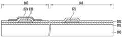
도 1a를 참조하면, 기판(100)은 화소 영역(140) 및 비화소 영역(150)을 포함한다. 비화소 영역(150)은 화소 영역(140)을 둘러싸는 영역 또는 화소 영역(140)을 제외한 나머지 영역이 된다.Referring to FIG. 1A, the
화소 영역(140)의 기판(100)에는 주사 라인(142) 및 데이터 라인(144)이 서로 교차되도록 배치되고, 주사 라인(142) 및 데이터 라인(144) 사이에는 복수의 화 소부(146)가 매트릭스 방식으로 연결된다. 화소부(146)는 유기전계발광 다이오드, 유기전계발광 다이오드의 동작을 제어하기 위한 박막 트랜지스터 및 신호를 유지시키기 위한 캐패시터를 포함할 수 있다.The
비화소 영역(150)의 기판(100)에는 화소 영역(140)의 주사 라인(142) 및 데이터 라인(144)으로부터 연장된 주사 라인(142) 및 데이터 라인(144), 유기전계발광 다이오드의 동작을 위한 전원공급 라인(도시안됨) 그리고 패드(180)를 통해 외부로부터 제공된 신호를 처리하여 주사 라인(142) 및 데이터 라인(144)으로 공급하는 주사 구동부(160) 및 데이터 구동부(170)가 배치된다. 주사 구동부(160) 및 데이터 구동부(170)는 패드(180)를 통해 외부로부터 제공되는 신호를 주사 신호 및 데이터 신호로 변환하여 각 화소를 선택적으로 구동시키는 구동회로를 포함한다.The operation of the
도 1b를 참조하면, 화소부(146)가 형성된 기판(100) 상부에는 화소 영역(140)을 밀봉시키기 위한 봉지 기판(200)이 배치되며, 화소 영역(140)을 둘러싸도록 배치되는 밀봉재(300)에 의해 봉지 기판(200)이 기판(100)에 합착된다.Referring to FIG. 1B, an encapsulation substrate 200 for encapsulating the
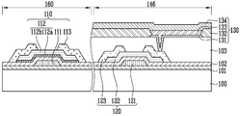
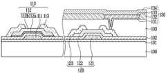
도 2는 도 1a에 도시된 화소부(146) 및 주사 구동부(160)를 보다 상세하게 설명하기 위한 단면도이다. 설명의 편의를 위하여 화소부(146)는 박막 트랜지스터(120) 및 유기전계발광 다이오드(130)만을 도시하였고, 주사 구동부(160)는 박막 트랜지스터(120)만을 도시하였다. 도면에는 주사 구동부(160)만을 도시하였으나, 데이터 구동부(170)의 박막 트랜지스터도 동일한 구조로 형성된다.FIG. 2 is a cross-sectional view for describing the
도 2를 참조하면, 화소 영역(140) 및 비화소 영역(150)의 기판(100) 상에 버퍼층(101)이 형성된다. 도면에서 화소 영역(140)은 화소부(146)를 도시하며, 비화 소 영역(150)은 주사 구동부(160)를 도시한다.Referring to FIG. 2, a
주사 구동부(160)의 버퍼층(101) 상에는 구동회로를 구성하는 박막 트랜지스터(110)가 형성되고, 화소부(146)의 버퍼층(101) 상에는 스위치 역할을 하는 박막 트랜지스터(120)가 형성된다.The
주사 구동부(160)의 박막 트랜지스터(110)는 게이트 전극(111), 게이트 절연층(102)에 의해 게이트 전극(111)과 절연되는 활성층(112), 소스 및 드레인 영역의 활성층(112)과 연결되는 소스 및 드레인 전극(113)을 포함한다. 활성층(112)은 케리어 농도가 서로 다른(전도성이 서로 다른), 보다 상세하게는 케리어 농도가 높은 제 1 산화물 반도체층(112a)과, 제 1 산화물 반도체층(112a)보다 케리어 농도가 낮은 제 2 산화물 반도체층(112b)의 적층 구조로 형성된다. 즉, 실질적으로 채널이 형성되는 일부 두께(예를 들어, 1 내지 5㎚ 정도의 두께)는 상대적으로 케리어 농도가 높은(1e+19 내지 1e+21#/㎤) 제 1 산화물 반도체층(112a)으로 형성되고, 나머지 대부분의 두께(예를 들어, 10 내지 50㎚ 정도의 두께)는 상대적으로 케리어 농도가 낮은(1e+13 내지 1e+18#/㎤) 제 2 산화물 반도체층(112b)으로 형성된다. 예를 들어, 제 1 산화물 반도체층(112a)은 ITO(Indium-tin oxide), InZnO(IZO), InSnO, AlZnO, AlGaO 및 InGaO를 포함하는 군에서 선택될 수 있고, 제 2 산화물 반도체층(112b)은 산화아연(ZnO)이나, 갈륨(Ga), 인듐(In), 스태늄(Sn), 지르코늄(Zr), 하프늄(Hf), 카드뮴(Cd), 은(Ag), 구리(Cu), 게르마늄(Ge), 가돌리늄(Gd) 및 바나듐(V) 중 적어도 하나의 이온이 도핑된 산화아연(ZnO), 예를 들어, ZnO, ZnSnO, InGaZnO 등으로 형성될 수 있다. ITO, IZO 등은 대개 도전층으로 사용되지만, 증착 과정에서 두께를 얇게 조절하고 산소 농도를 조절하여 케리어 농도를 제어하면 반도체 특성을 가질 수 있다.The
한편, 화소부(146)의 박막 트랜지스터(120)는 게이트 전극(121), 게이트 절연층(102)에 의해 게이트 전극(121)과 절연되는 활성층(122), 소스 및 드레인 영역의 활성층(122)과 연결되는 소스 및 드레인 전극(123)을 포함하며, 활성층(122)은 박막 트랜지스터(110)의 활성층(112)을 구성하는 제 2 산화물 반도체층(112b)과 동일 층 또는 동일 물질의 산화물 반도체층으로 형성된다. 즉, 활성층(122)은 산화아연(ZnO)이나, 갈륨(Ga), 인듐(In), 스태늄(Sn), 지르코늄(Zr), 하프늄(Hf), 카드뮴(Cd), 은(Ag), 구리(Cu), 게르마늄(Ge), 가돌리늄(Gd) 및 바나듐(V) 중 적어도 하나의 이온이 도핑된 산화아연(ZnO), 예를 들어, ZnO, InGaZnO, InSnZnO, ZnSnO 등으로 형성될 수 있다.In the meantime, the
또한, 화소부(146)의 박막 트랜지스터(120)를 포함하는 상부에는 평탄화를 위하여 절연층(103)이 형성되고, 절연층(103)에는 박막 트랜지스터(120)의 소스 또는 드레인 전극(123)이 노출되도록 비아홀이 형성된다. 그리고 화소부(146)의 절연층(103) 상에는 상기 비아홀을 통해 박막 트랜지스터(120)의 소스 또는 드레인 전극(123)과 연결되도록 유기전계발광 다이오드(130)가 형성된다.In addition, an insulating
유기전계발광 다이오드(130)는 상기 비아홀을 통해 박막 트랜지스터(120)의 소스 또는 드레인 전극(123)과 연결되는 애노드 전극(131), 화소 정의막(132)에 의해 노출되는 발광 영역의 애노드 전극(131) 상에 형성된 유기 발광층(133) 및 유기 발광층(133)을 포함하는 화소 정의막(132) 상에 형성된 캐소드 전극(134)을 포함한 다. 유기 발광층(133)은 정공 주입층, 정공 수송층, 전자 수송층 및 전자 주입층을 포함할 수 있다.The organic
상기와 같이 본 발명에 따르면, 화소부(146) 박막 트랜지스터(120)의 활성층(122)은 산화물 반도체층으로 형성되고, 구동부(160, 170) 박막 트랜지스터(110)의 활성층(112)은 케리어 농도가 서로 다른(전도성이 서로 다른) 제 1 산화물 반도체층(112a) 및 제 2 산화물 반도체층(112b)의 적층 구조로 형성된다. 즉, 상대적으로 낮은 전하 이동도(약 10 내지 20㎠/V.sec) 및 높은 특성 균일도가 요구되는 화소부(146) 박막 트랜지스터(120)의 활성층(122)은 ZnO, InGaZnO, InSnZnO, ZnSnO 등의 산화물 반도체층으로 형성되고, 상대적으로 높은 전하 이동도(약 50 내지 130㎠/V.sec)가 요구되는 구동부(160, 170) 박막 트랜지스터(110)의 활성층(112)은 상대적으로 케리어 농도가 높은(전도성이 높은) ITO, IZO 등의 제 1 산화물 반도체층(112a)과, 상대적으로 케리어 농도가 낮은(전도성이 낮은) ZnO, InGaZnO, InSnZnO, ZnSnO 등의 제 2 산화물 반도체층(112b)으로 형성된다. 따라서 구동부(160, 170) 박막 트랜지스터(110)는 채널이 제 2 산화물 반도체층(112b)보다 케리어 농도가 높은 제 1 산화물 반도체층(112a)에 형성되기 때문에 높은 전하 이동도를 가지며, 화소부(146) 박막 트랜지스터(120)는 채널이 제 2 산화물 반도체층(122)에 형성되기 때문에 안정적이고 균일한 특성을 가진다.As described above, the
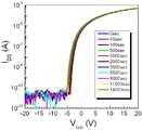
도 3a 내지 도 3c는 게이트 전극과 소스 전극에 인가되는 전압(VGS)의 변화에 따른 드레인 전극과 소스 전극의 전류(IDS) 변화를 측정한 그래프로서, 도 3a는 활성층(112)이 InZnO(112a) 및 GaInZnO(112b)로 형성된 구동부(160) 박막 트랜지스터(110)이고, 도 3b는 활성층(112)이 ITO(112a) 및 GaInZnO(112b)로 형성된 구동부(160) 박막 트랜지스터(110)이며, 도 3c는 활성층(122)이 GaInZnO로 형성된 화소부(146) 박막 트랜지스터(120)이다. 소자의 크기가 동일한 경우 도 3a 및 도 3b의 구동부(160) 박막 트랜지스터(110)가 도 3c의 화소부(146) 박막 트랜지스터(120)에 비해 전류(on current) 특성이 우수하며, 이는 전하 이동도의 차이에 의한 것임을 알 수 있다.3A to 3C are graphs illustrating changes in current IDS of the drain electrode and the source electrode according to the change of the voltage VGS applied to the gate electrode and the source electrode, and FIG. 3A shows that the
도 4a 내지 도 4d는 본 발명에 따른 유기전계발광 표시 장치의 제조 방법을 설명하기 위한 단면도이다.4A to 4D are cross-sectional views illustrating a method of manufacturing an organic light emitting display device according to the present invention.
도 4a를 참조하면, 화소 영역(140) 및 비화소 영역(150)이 정의된 기판(100)을 준비한다. 도면에서 화소 영역(140)은 화소부(146)를 도시하며, 비화소 영역(150)은 주사 구동부(160)를 도시한다.Referring to FIG. 4A, a
화소 영역(140) 및 비화소 영역(150)의 기판(100) 상에 버퍼층(101)을 형성하고, 주사 구동부(160) 및 화소부(146)의 버퍼층(101) 상에 박막 트랜지스터(110 및 120)의 게이트 전극(111 및 121)을 각각 형성한다.The
게이트 전극(111 및 121)을 포함하는 전체 상부에 게이트 절연층(102) 및 제 1 산화물 반도체층(112a)을 순차적으로 형성한 후 제 1 산화물 반도체층(112a)을 패터닝하여 주사 구동부(160)의 게이트 절연층(102) 상에 제 1 산화물 반도체층(112a)을 잔류시킨다. 제 1 산화물 반도체층(112a)은 ITO, IZO, InSnO, AlZnO, AlGaO, InGaO 등을 1 내지 5㎚ 정도의 두께로 증착하여 형성한다.The
도 4b를 참조하면, 제 1 산화물 반도체층(112a)을 포함하는 전체 상부에 제 2 산화물 반도체층(112b)을 형성한 후 패터닝하여 주사 구동부(160)에는 제 1 산화물 반도체층(112a) 및 제 2 산화물 반도체층(112b)의 적층 구조로 이루어진 활성층(112)을 형성하고, 화소부(146)에는 제 2 산화물 반도체층과 동일 층으로 이루어진 활성층(122)을 형성한다. 제 2 산화물 반도체층(112b)은 ZnO, ZnSnO, InGaZnO 등으로 형성한다.Referring to FIG. 4B, the second oxide semiconductor layer 112b is formed over the entire surface including the first
도 4c를 참조하면, 활성층(112 및 122)을 포함하는 전체 상부에 도전층을 형성한 후 패터닝하여 활성층(112 및 122)의 소스 및 드레인 영역과 연결되도록 소스 및 드레인 전극(113 및 123)을 각각 형성한다.Referring to FIG. 4C, the source and drain
도 4d를 참조하면, 박막 트랜지스터(110 및 120)를 포함하는 상부 또는 박막 트랜지스터(120)를 포함하는 상부에 평탄화를 위하여 절연층(103)을 형성한 후 박막 트랜지스터(120)의 소스 또는 드레인 전극(123)이 노출되도록 비아홀을 형성한다. 그리고 화소부(146)의 절연층(103) 상에 상기 비아홀을 통해 박막 트랜지스터(120)의 소스 또는 드레인 전극(123)과 연결되는 애노드 전극(131)을 형성한다.Referring to FIG. 4D, a source or drain electrode of the
애노드 전극(131)을 포함하는 상부에 화소 정의막(132)을 형성한 패터닝하여 발광영역의 애노드 전극(131)이 노출되도록 개구부를 형성하고, 개구부의 애노드 전극(131) 상에 유기 발광층(133)을 형성한다. 유기 발광층(133)은 정공 주입층, 정공 수송층, 전자 수송층 및 전자 주입층을 포함할 수 있다.The
이 후 유기 발광층(133)을 포함하는 화소 정의막(132) 상에 캐소드 전극(134)을 형성하여 유기전계발광 다이오드(130)를 완성한다.Thereafter, the
이상에서와 같이 상세한 설명과 도면을 통해 본 발명의 최적 실시예를 개시하였다. 용어들은 단지 본 발명을 설명하기 위한 목적에서 사용된 것이지 의미 한정이나 특허청구범위에 기재된 본 발명의 범위를 제한하기 위하여 사용된 것은 아니다. 그러므로 본 기술 분야의 통상의 지식을 가진 자라면 이로부터 다양한 변형 및 균등한 타 실시예가 가능하다는 점을 이해할 것이다. 따라서 본 발명의 진정한 기술적 보호 범위는 첨부된 특허청구범위의 기술적 사상에 의해 정해져야 할 것이다.As described above, the preferred embodiment of the present invention has been disclosed through the detailed description and the drawings. The terms are used only for the purpose of describing the present invention and are not used to limit the scope of the present invention as defined in the meaning or claims. Therefore, those skilled in the art will understand that various modifications and equivalent other embodiments are possible from this. Therefore, the true technical protection scope of the present invention will be defined by the technical spirit of the appended claims.
도 1a 및 1b는 본 발명에 따른 유기전계발광 표시 장치를 설명하기 위한 평면도 및 단면도.1A and 1B are a plan view and a cross-sectional view for explaining an organic light emitting display device according to the present invention.
도 2는 도 1a에 도시된 화소부 및 주사 구동부를 설명하기 위한 단면도.FIG. 2 is a sectional view for explaining the pixel portion and the scan driver shown in FIG. 1A; FIG.
도 3a 내지 도 3c는 게이트 전극과 소스 전극에 인가되는 전압(VGS)의 변화에 따른 드레인 전극과 소스 전극의 전류(IDS) 변화를 측정한 그래프.3A to 3C are graphs illustrating changes in current IDS of the drain electrode and the source electrode according to the change of the voltage VGS applied to the gate electrode and the source electrode.
도 4a 내지 도 4d는 본 발명에 따른 유기전계발광 표시 장치의 제조 방법을 설명하기 위한 단면도.4A to 4D are cross-sectional views illustrating a method of manufacturing an organic light emitting display device according to the present invention.
<도면의 주요 부분에 대한 부호의 설명><Explanation of symbols for the main parts of the drawings>
100: 기판101: 버퍼층100: substrate 101: buffer layer
102: 게이트 절연층103: 절연층102: gate insulating layer 103: insulating layer
110, 120: 박막 트랜지스터111, 121: 게이트 전극110 and 120
112, 122: 활성층112a: 제 1 산화물 반도체층112 and 122:
112b: 제 2 산화물 반도체층113, 123: 소스 및 드레인 전극112b: second oxide semiconductor layers 113 and 123: source and drain electrodes
130: 유기전계발광 다이오드131: 애노드 전극130: organic light emitting diode 131: anode electrode
132: 화소 정의막133: 유기 발광층132: pixel defining layer 133: organic light emitting layer
134: 캐소드 전극140: 화소 영역134: cathode electrode 140: pixel region
142: 주사 라인144: 데이터 라인142: scan line 144: data line
146: 화소부150: 비화소 영역146: pixel portion 150: non-pixel region
160: 주사 구동부170: 데이터 구동부160: scan driver 170: data driver
180: 패드200: 봉지 기판180: pad 200: sealing substrate
300: 밀봉재300: sealing material
Claims (17)
Translated fromKoreanPriority Applications (7)
| Application Number | Priority Date | Filing Date | Title |
|---|---|---|---|
| KR1020090002242AKR101034686B1 (en) | 2009-01-12 | 2009-01-12 | Organic light emitting display device and manufacturing method thereof |
| JP2009070440AJP5274327B2 (en) | 2009-01-12 | 2009-03-23 | Organic electroluminescent display device and manufacturing method thereof |
| US12/654,938US8436342B2 (en) | 2009-01-12 | 2010-01-08 | Organic light emitting display device and method of manufacturing the same |
| AT10150419TATE523898T1 (en) | 2009-01-12 | 2010-01-11 | ORGANIC LIGHT EMITTING DISPLAY DEVICE AND METHOD FOR PRODUCING THE SAME |
| CN201010002358XACN101794809B (en) | 2009-01-12 | 2010-01-11 | Organic light emitting display device and method of manufacturing the same |
| EP10150419AEP2207206B1 (en) | 2009-01-12 | 2010-01-11 | Organic light emitting display device and method of manufacturing the same |
| TW099100651ATWI423436B (en) | 2009-01-12 | 2010-01-12 | Organic light emitting display device and method of manufacturing same |
Applications Claiming Priority (1)
| Application Number | Priority Date | Filing Date | Title |
|---|---|---|---|
| KR1020090002242AKR101034686B1 (en) | 2009-01-12 | 2009-01-12 | Organic light emitting display device and manufacturing method thereof |
Publications (2)
| Publication Number | Publication Date |
|---|---|
| KR20100082940A KR20100082940A (en) | 2010-07-21 |
| KR101034686B1true KR101034686B1 (en) | 2011-05-16 |
Family
ID=42124279
Family Applications (1)
| Application Number | Title | Priority Date | Filing Date |
|---|---|---|---|
| KR1020090002242AActiveKR101034686B1 (en) | 2009-01-12 | 2009-01-12 | Organic light emitting display device and manufacturing method thereof |
Country Status (7)
| Country | Link |
|---|---|
| US (1) | US8436342B2 (en) |
| EP (1) | EP2207206B1 (en) |
| JP (1) | JP5274327B2 (en) |
| KR (1) | KR101034686B1 (en) |
| CN (1) | CN101794809B (en) |
| AT (1) | ATE523898T1 (en) |
| TW (1) | TWI423436B (en) |
Cited By (1)
| Publication number | Priority date | Publication date | Assignee | Title |
|---|---|---|---|---|
| KR101406838B1 (en) | 2012-05-14 | 2014-06-16 | 연세대학교 산학협력단 | Oxide semiconductor and method of forming the same |
Families Citing this family (82)
| Publication number | Priority date | Publication date | Assignee | Title |
|---|---|---|---|---|
| US8367486B2 (en)* | 2009-02-05 | 2013-02-05 | Semiconductor Energy Laboratory Co., Ltd. | Transistor and method for manufacturing the transistor |
| JP5504008B2 (en) | 2009-03-06 | 2014-05-28 | 株式会社半導体エネルギー研究所 | Semiconductor device |
| WO2011013523A1 (en)* | 2009-07-31 | 2011-02-03 | Semiconductor Energy Laboratory Co., Ltd. | Semiconductor device and method for manufacturing the same |
| KR101041144B1 (en)* | 2009-08-13 | 2011-06-13 | 삼성모바일디스플레이주식회사 | Thin film transistor, manufacturing method thereof and organic light emitting display device comprising same |
| KR20230165355A (en)* | 2009-09-16 | 2023-12-05 | 가부시키가이샤 한도오따이 에네루기 켄큐쇼 | Display device |
| WO2011034012A1 (en)* | 2009-09-16 | 2011-03-24 | Semiconductor Energy Laboratory Co., Ltd. | Logic circuit, light emitting device, semiconductor device, and electronic device |
| WO2011065243A1 (en) | 2009-11-28 | 2011-06-03 | Semiconductor Energy Laboratory Co., Ltd. | Semiconductor device and manufacturing method thereof |
| KR101825345B1 (en) | 2009-11-28 | 2018-02-05 | 가부시키가이샤 한도오따이 에네루기 켄큐쇼 | Stacked oxide material, semiconductor device, and method for manufacturing the semiconductor device |
| WO2011065210A1 (en) | 2009-11-28 | 2011-06-03 | Semiconductor Energy Laboratory Co., Ltd. | Stacked oxide material, semiconductor device, and method for manufacturing the semiconductor device |
| WO2011074407A1 (en) | 2009-12-18 | 2011-06-23 | Semiconductor Energy Laboratory Co., Ltd. | Semiconductor device and method for manufacturing the same |
| KR102542681B1 (en) | 2010-01-20 | 2023-06-14 | 가부시키가이샤 한도오따이 에네루기 켄큐쇼 | Electronic device |
| KR102129540B1 (en) | 2010-01-20 | 2020-07-03 | 가부시키가이샤 한도오따이 에네루기 켄큐쇼 | Display device |
| KR101878206B1 (en)* | 2010-03-05 | 2018-07-16 | 가부시키가이샤 한도오따이 에네루기 켄큐쇼 | Manufacturing method of oxide semiconductor film and manufacturing method of transistor |
| KR101050466B1 (en)* | 2010-03-12 | 2011-07-20 | 삼성모바일디스플레이주식회사 | Capacitor of OLED Display and OLED Display |
| US8884282B2 (en)* | 2010-04-02 | 2014-11-11 | Semiconductor Energy Laboratory Co., Ltd. | Semiconductor device |
| KR101101109B1 (en) | 2010-06-01 | 2012-01-03 | 삼성모바일디스플레이주식회사 | Organic light emitting display device |
| JP2012256819A (en)* | 2010-09-08 | 2012-12-27 | Semiconductor Energy Lab Co Ltd | Semiconductor device |
| JP2012256821A (en)* | 2010-09-13 | 2012-12-27 | Semiconductor Energy Lab Co Ltd | Memory device |
| KR20120042029A (en)* | 2010-10-22 | 2012-05-03 | 삼성모바일디스플레이주식회사 | Display device and method for manufacturing the same |
| TWI562379B (en) | 2010-11-30 | 2016-12-11 | Semiconductor Energy Lab Co Ltd | Semiconductor device and method for manufacturing semiconductor device |
| JP5723262B2 (en)* | 2010-12-02 | 2015-05-27 | 株式会社神戸製鋼所 | Thin film transistor and sputtering target |
| WO2012081591A1 (en) | 2010-12-17 | 2012-06-21 | Semiconductor Energy Laboratory Co., Ltd. | Oxide material and semiconductor device |
| TWI401797B (en)* | 2010-12-28 | 2013-07-11 | Ind Tech Res Inst | Active device array and organic light emitting diode pixel array manufacturing method |
| US8952377B2 (en) | 2011-07-08 | 2015-02-10 | Semiconductor Energy Laboratory Co., Ltd. | Semiconductor device and manufacturing method thereof |
| WO2013021632A1 (en)* | 2011-08-11 | 2013-02-14 | 出光興産株式会社 | Thin-film transistor |
| CN102769039A (en)* | 2012-01-13 | 2012-11-07 | 京东方科技集团股份有限公司 | A kind of thin film transistor and its manufacturing method, array substrate and display device |
| KR101942980B1 (en) | 2012-01-17 | 2019-01-29 | 삼성디스플레이 주식회사 | Semiconductor device and method for forming the same |
| KR101372734B1 (en)* | 2012-02-15 | 2014-03-13 | 연세대학교 산학협력단 | Thin film transistor using liquid-phase process and method for fabricating the same |
| KR101950834B1 (en)* | 2012-03-06 | 2019-02-21 | 엘지디스플레이 주식회사 | Oxide thin film transistor and method for fabricating the same |
| US9219164B2 (en)* | 2012-04-20 | 2015-12-22 | Semiconductor Energy Laboratory Co., Ltd. | Semiconductor device with oxide semiconductor channel |
| CN102637742A (en)* | 2012-04-26 | 2012-08-15 | 北京大学 | Oxide semiconductor thin-film transistor and preparation method thereof |
| US9048323B2 (en) | 2012-04-30 | 2015-06-02 | Semiconductor Energy Laboratory Co., Ltd. | Semiconductor device |
| KR20250009548A (en) | 2012-05-10 | 2025-01-17 | 가부시키가이샤 한도오따이 에네루기 켄큐쇼 | Semiconductor device |
| CN104380473B (en) | 2012-05-31 | 2017-10-13 | 株式会社半导体能源研究所 | Semiconductor device |
| KR102113160B1 (en) | 2012-06-15 | 2020-05-20 | 가부시키가이샤 한도오따이 에네루기 켄큐쇼 | Semiconductor device |
| KR102161077B1 (en) | 2012-06-29 | 2020-09-29 | 가부시키가이샤 한도오따이 에네루기 켄큐쇼 | Semiconductor device |
| JP6134598B2 (en) | 2012-08-02 | 2017-05-24 | 株式会社半導体エネルギー研究所 | Semiconductor device |
| US9356156B2 (en)* | 2013-05-24 | 2016-05-31 | Cbrite Inc. | Stable high mobility MOTFT and fabrication at low temperature |
| KR102162794B1 (en) | 2013-05-30 | 2020-10-08 | 삼성디스플레이 주식회사 | Back plane of display and manufacturing method for the same |
| KR102101398B1 (en)* | 2013-06-13 | 2020-04-16 | 엘지디스플레이 주식회사 | Oxide semiconductor thin film transistor and Display Device and Method of manufacturing the sames |
| KR20150004091A (en) | 2013-07-02 | 2015-01-12 | 삼성디스플레이 주식회사 | Organic Light Emitting Display Device and Fabricating Method Thereof |
| US9564478B2 (en) | 2013-08-26 | 2017-02-07 | Apple Inc. | Liquid crystal displays with oxide-based thin-film transistors |
| US9818765B2 (en) | 2013-08-26 | 2017-11-14 | Apple Inc. | Displays with silicon and semiconducting oxide thin-film transistors |
| KR102264987B1 (en)* | 2013-12-02 | 2021-06-16 | 가부시키가이샤 한도오따이 에네루기 켄큐쇼 | Display device |
| US9349751B2 (en) | 2013-12-12 | 2016-05-24 | Semiconductor Energy Laboratory Co., Ltd. | Semiconductor device |
| US9397149B2 (en)* | 2013-12-27 | 2016-07-19 | Semiconductor Energy Laboratory Co., Ltd. | Semiconductor device |
| TWI658597B (en)* | 2014-02-07 | 2019-05-01 | 日商半導體能源研究所股份有限公司 | Semiconductor device |
| TWI772799B (en)* | 2014-05-09 | 2022-08-01 | 日商半導體能源研究所股份有限公司 | Semiconductor device |
| KR102157689B1 (en)* | 2014-06-27 | 2020-09-21 | 엘지디스플레이 주식회사 | Thin film array transistor substrate for flat panel display device |
| KR102308621B1 (en)* | 2014-07-15 | 2021-10-05 | 삼성디스플레이 주식회사 | Thin film transistor array panel and method of manufacturing the same |
| WO2016056204A1 (en)* | 2014-10-10 | 2016-04-14 | 株式会社Joled | Thin film transistor substrate, method for manufacturing thin film transistor substrate, and display panel |
| KR102423678B1 (en)* | 2015-09-25 | 2022-07-21 | 삼성디스플레이 주식회사 | Thin film transistor array panel and method of manufacturing the same |
| US9818344B2 (en) | 2015-12-04 | 2017-11-14 | Apple Inc. | Display with light-emitting diodes |
| JP2017143135A (en)* | 2016-02-09 | 2017-08-17 | 株式会社ジャパンディスプレイ | Thin film transistor |
| CN106057826A (en)* | 2016-08-08 | 2016-10-26 | 京东方科技集团股份有限公司 | Array substrate and manufacturing method thereof, and display apparatus |
| CN106449667B (en)* | 2016-12-21 | 2017-12-22 | 京东方科技集团股份有限公司 | Array base palte and preparation method thereof, display device |
| CN110383493B (en)* | 2017-03-09 | 2023-06-02 | 夏普株式会社 | Active matrix substrate and method for manufacturing same |
| JP2018195632A (en)* | 2017-05-15 | 2018-12-06 | 株式会社ジャパンディスプレイ | Semiconductor device and display device |
| CN109863598A (en) | 2017-09-29 | 2019-06-07 | 京东方科技集团股份有限公司 | Array substrate, display device and method of manufacturing array substrate |
| KR102585853B1 (en)* | 2017-10-12 | 2023-10-06 | 엘지디스플레이 주식회사 | Substrate for display and display including the same |
| KR20200019308A (en)* | 2018-08-13 | 2020-02-24 | 삼성디스플레이 주식회사 | Organic light emitting diode display device |
| KR102604006B1 (en)* | 2018-08-14 | 2023-11-21 | 엘지전자 주식회사 | Display device using semiconductor light emitting diode and method for manufacturing the same |
| KR102689232B1 (en)* | 2018-09-20 | 2024-07-29 | 삼성디스플레이 주식회사 | Transistor substrate, method of manufacturing the same, and display device including the same |
| WO2020089733A1 (en) | 2018-11-02 | 2020-05-07 | 株式会社半導体エネルギー研究所 | Semiconductor device |
| CN110010626B (en)* | 2019-04-11 | 2022-04-29 | 京东方科技集团股份有限公司 | Display substrate, manufacturing method thereof, and display device |
| KR102864580B1 (en) | 2019-06-04 | 2025-09-24 | 어플라이드 머티어리얼스, 인코포레이티드 | Thin film transistor |
| CN110164875A (en) | 2019-06-06 | 2019-08-23 | 京东方科技集团股份有限公司 | Array substrate and preparation method thereof, display panel, display device |
| KR102813716B1 (en)* | 2019-07-17 | 2025-05-28 | 삼성디스플레이 주식회사 | Display device |
| KR102814905B1 (en)* | 2019-07-17 | 2025-05-30 | 삼성디스플레이 주식회사 | Display device and method for fabricating the same |
| CN110739316A (en)* | 2019-10-29 | 2020-01-31 | 合肥维信诺科技有限公司 | Array substrate, display panel and manufacturing method of array substrate |
| US20210193049A1 (en)* | 2019-12-23 | 2021-06-24 | Apple Inc. | Electronic Display with In-Pixel Compensation and Oxide Drive Transistors |
| US11624126B2 (en) | 2020-06-16 | 2023-04-11 | Ohio State Innovation Foundation | Deposition of single phase beta-(AlxGa1-x)2O3 thin films with 0.28< =x<=0.7 on beta Ga2O3(100) or (−201) substrates by chemical vapor deposition |
| CN114730738A (en)* | 2020-09-22 | 2022-07-08 | 京东方科技集团股份有限公司 | Array substrate, display panel and display device |
| CN115084275B (en)* | 2021-03-15 | 2024-09-27 | 京东方科技集团股份有限公司 | Metal oxide TFT and manufacturing method, X-ray detector and display panel |
| US20220384366A1 (en)* | 2021-06-01 | 2022-12-01 | Cree, Inc. | Multilayer encapsulation for humidity robustness and related fabrication methods |
| CN113257841B (en)* | 2021-07-19 | 2021-11-16 | 深圳市柔宇科技股份有限公司 | TFT substrate and preparation method thereof, display and electronic device |
| CN114005841A (en)* | 2021-10-29 | 2022-02-01 | 京东方科技集团股份有限公司 | A metal oxide thin film transistor backplane |
| WO2023092562A1 (en)* | 2021-11-29 | 2023-06-01 | 京东方科技集团股份有限公司 | Metal oxide thin film transistor, and array substrate and preparation method therefor |
| US20230200150A1 (en)* | 2021-12-22 | 2023-06-22 | Shenzhen China Star Optoelectronics Semiconductor Display Technology Co., Ltd. | Display panel |
| CN114300487A (en)* | 2021-12-30 | 2022-04-08 | 广州华星光电半导体显示技术有限公司 | TFT substrate and preparation method thereof, display panel and display device |
| US20230317634A1 (en)* | 2022-04-05 | 2023-10-05 | Applied Materials, Inc. | Coatings with diffusion barriers for corrosion and contamination protection |
| US20240304631A1 (en)* | 2022-05-31 | 2024-09-12 | Boe Technology Group Co., Ltd. | Drive backplane, method for manufacturing same, and display panel |
Citations (2)
| Publication number | Priority date | Publication date | Assignee | Title |
|---|---|---|---|---|
| US20070120785A1 (en) | 2005-11-30 | 2007-05-31 | Semiconductor Energy Laboratory Co., Ltd. | Display device |
| WO2008126878A1 (en) | 2007-04-10 | 2008-10-23 | Fujifilm Corporation | Organic electroluminescence display device |
Family Cites Families (14)
| Publication number | Priority date | Publication date | Assignee | Title |
|---|---|---|---|---|
| JP4166105B2 (en) | 2003-03-06 | 2008-10-15 | シャープ株式会社 | Semiconductor device and manufacturing method thereof |
| JP3772889B2 (en)* | 2003-05-19 | 2006-05-10 | セイコーエプソン株式会社 | Electro-optical device and driving device thereof |
| US7262463B2 (en)* | 2003-07-25 | 2007-08-28 | Hewlett-Packard Development Company, L.P. | Transistor including a deposited channel region having a doped portion |
| KR100506740B1 (en)* | 2003-12-23 | 2005-08-08 | 삼성전기주식회사 | Nitride semiconductor light emitting device and method of manufacturing the same |
| KR100623690B1 (en) | 2004-06-30 | 2006-09-19 | 삼성에스디아이 주식회사 | Flat panel display and manufacturing method thereof |
| JP5138163B2 (en) | 2004-11-10 | 2013-02-06 | キヤノン株式会社 | Field effect transistor |
| EP2453481B1 (en)* | 2004-11-10 | 2017-01-11 | Canon Kabushiki Kaisha | Field effect transistor with amorphous oxide |
| KR100685831B1 (en) | 2005-04-29 | 2007-02-22 | 삼성에스디아이 주식회사 | Organic electroluminescent device and manufacturing method thereof |
| CN101283388B (en)* | 2005-10-05 | 2011-04-13 | 出光兴产株式会社 | TFT substrate and method for manufacturing TFT substrate |
| TW200801513A (en) | 2006-06-29 | 2008-01-01 | Fermiscan Australia Pty Ltd | Improved process |
| KR100712176B1 (en) | 2006-12-14 | 2007-04-27 | 삼성에스디아이 주식회사 | Organic electroluminescent device and manufacturing method thereof |
| JP5121254B2 (en)* | 2007-02-28 | 2013-01-16 | キヤノン株式会社 | Thin film transistor and display device |
| US9176353B2 (en)* | 2007-06-29 | 2015-11-03 | Semiconductor Energy Laboratory Co., Ltd. | Liquid crystal display device |
| TWI501319B (en)* | 2008-12-26 | 2015-09-21 | Semiconductor Energy Lab | Semiconductor device and manufacturing method thereof |
- 2009
- 2009-01-12KRKR1020090002242Apatent/KR101034686B1/enactiveActive
- 2009-03-23JPJP2009070440Apatent/JP5274327B2/enactiveActive
- 2010
- 2010-01-08USUS12/654,938patent/US8436342B2/enactiveActive
- 2010-01-11ATAT10150419Tpatent/ATE523898T1/ennot_activeIP Right Cessation
- 2010-01-11CNCN201010002358XApatent/CN101794809B/enactiveActive
- 2010-01-11EPEP10150419Apatent/EP2207206B1/enactiveActive
- 2010-01-12TWTW099100651Apatent/TWI423436B/enactive
Patent Citations (2)
| Publication number | Priority date | Publication date | Assignee | Title |
|---|---|---|---|---|
| US20070120785A1 (en) | 2005-11-30 | 2007-05-31 | Semiconductor Energy Laboratory Co., Ltd. | Display device |
| WO2008126878A1 (en) | 2007-04-10 | 2008-10-23 | Fujifilm Corporation | Organic electroluminescence display device |
Cited By (1)
| Publication number | Priority date | Publication date | Assignee | Title |
|---|---|---|---|---|
| KR101406838B1 (en) | 2012-05-14 | 2014-06-16 | 연세대학교 산학협력단 | Oxide semiconductor and method of forming the same |
Also Published As
| Publication number | Publication date |
|---|---|
| CN101794809B (en) | 2012-11-28 |
| CN101794809A (en) | 2010-08-04 |
| TW201030967A (en) | 2010-08-16 |
| JP5274327B2 (en) | 2013-08-28 |
| KR20100082940A (en) | 2010-07-21 |
| US20100176383A1 (en) | 2010-07-15 |
| JP2010161327A (en) | 2010-07-22 |
| EP2207206B1 (en) | 2011-09-07 |
| US8436342B2 (en) | 2013-05-07 |
| ATE523898T1 (en) | 2011-09-15 |
| TWI423436B (en) | 2014-01-11 |
| EP2207206A1 (en) | 2010-07-14 |
Similar Documents
| Publication | Publication Date | Title |
|---|---|---|
| KR101034686B1 (en) | Organic light emitting display device and manufacturing method thereof | |
| KR101048965B1 (en) | Organic electroluminescent display | |
| KR101073542B1 (en) | Organic light emitting diode display and method for manufacturing the same | |
| KR100941850B1 (en) | Thin film transistor, its manufacturing method, and flat panel display device comprising thin film transistor | |
| KR100958006B1 (en) | Thin film transistor, its manufacturing method, and flat panel display device comprising thin film transistor | |
| KR100963003B1 (en) | Thin film transistor, its manufacturing method, and flat panel display device comprising thin film transistor | |
| KR101056229B1 (en) | An organic light emitting display device comprising a thin film transistor, a method of manufacturing the same, and a thin film transistor | |
| CN101621075B (en) | Thin film transistor, method of manufacturing the same and flat panel display device having the same | |
| KR101048996B1 (en) | Thin film transistor and flat panel display having same | |
| KR101113370B1 (en) | Thin Film Transistor and Organic Light Emitting Display device using thereof | |
| KR20090124527A (en) | Thin film transistor, its manufacturing method, and flat panel display device comprising thin film transistor | |
| KR102565380B1 (en) | Thin film transistor substrate | |
| KR20110037220A (en) | An organic light emitting display device comprising a thin film transistor, a method of manufacturing the same, and a thin film transistor | |
| KR102530003B1 (en) | Transistor array panel and display device including the same | |
| CN101621076A (en) | Thin film transistor, method of manufacturing the same and flat panel display device having the same | |
| KR20100015100A (en) | Thin film transistor, method of manufacturing the thin film transistor and flat panel display device having the thin film transistor | |
| KR20090105561A (en) | Semiconductor device and flat panel display device having same | |
| KR20150043075A (en) | Display device and method for manufacturing thereof | |
| KR100793105B1 (en) | Flat panel display device including thin film transistor and thin film transistor and manufacturing method thereof | |
| KR100941855B1 (en) | Thin film transistor, its manufacturing method, and flat panel display device comprising thin film transistor | |
| TWI874048B (en) | Thin film transistor, method for manufacturing the same and display apparatus comprising the same | |
| TW202527717A (en) | Thin film transistor substrate and display device using the same |
Legal Events
| Date | Code | Title | Description |
|---|---|---|---|
| A201 | Request for examination | ||
| PA0109 | Patent application | Patent event code:PA01091R01D Comment text:Patent Application Patent event date:20090112 | |
| PA0201 | Request for examination | ||
| PG1501 | Laying open of application | ||
| E902 | Notification of reason for refusal | ||
| PE0902 | Notice of grounds for rejection | Comment text:Notification of reason for refusal Patent event date:20100831 Patent event code:PE09021S01D | |
| AMND | Amendment | ||
| E601 | Decision to refuse application | ||
| PE0601 | Decision on rejection of patent | Patent event date:20110128 Comment text:Decision to Refuse Application Patent event code:PE06012S01D Patent event date:20100831 Comment text:Notification of reason for refusal Patent event code:PE06011S01I | |
| AMND | Amendment | ||
| J201 | Request for trial against refusal decision | ||
| PJ0201 | Trial against decision of rejection | Patent event date:20110224 Comment text:Request for Trial against Decision on Refusal Patent event code:PJ02012R01D Patent event date:20110128 Comment text:Decision to Refuse Application Patent event code:PJ02011S01I Appeal kind category:Appeal against decision to decline refusal Decision date:20110405 Appeal identifier:2011101001401 Request date:20110224 | |
| PB0901 | Examination by re-examination before a trial | Comment text:Amendment to Specification, etc. Patent event date:20110224 Patent event code:PB09011R02I Comment text:Request for Trial against Decision on Refusal Patent event date:20110224 Patent event code:PB09011R01I Comment text:Amendment to Specification, etc. Patent event date:20101029 Patent event code:PB09011R02I | |
| B701 | Decision to grant | ||
| PB0701 | Decision of registration after re-examination before a trial | Patent event date:20110405 Comment text:Decision to Grant Registration Patent event code:PB07012S01D Patent event date:20110329 Comment text:Transfer of Trial File for Re-examination before a Trial Patent event code:PB07011S01I | |
| GRNT | Written decision to grant | ||
| PR0701 | Registration of establishment | Comment text:Registration of Establishment Patent event date:20110504 Patent event code:PR07011E01D | |
| PR1002 | Payment of registration fee | Payment date:20110504 End annual number:3 Start annual number:1 | |
| PG1601 | Publication of registration | ||
| FPAY | Annual fee payment | Payment date:20140430 Year of fee payment:4 | |
| PR1001 | Payment of annual fee | Payment date:20140430 Start annual number:4 End annual number:4 | |
| FPAY | Annual fee payment | Payment date:20150430 Year of fee payment:5 | |
| PR1001 | Payment of annual fee | Payment date:20150430 Start annual number:5 End annual number:5 | |
| FPAY | Annual fee payment | Payment date:20180502 Year of fee payment:8 | |
| PR1001 | Payment of annual fee | Payment date:20180502 Start annual number:8 End annual number:8 | |
| FPAY | Annual fee payment | Payment date:20190429 Year of fee payment:9 | |
| PR1001 | Payment of annual fee | Payment date:20190429 Start annual number:9 End annual number:9 | |
| PR1001 | Payment of annual fee | Payment date:20200428 Start annual number:10 End annual number:10 | |
| PR1001 | Payment of annual fee | Payment date:20210503 Start annual number:11 End annual number:11 | |
| PR1001 | Payment of annual fee | Payment date:20220425 Start annual number:12 End annual number:12 | |
| PR1001 | Payment of annual fee | Payment date:20230502 Start annual number:13 End annual number:13 | |
| PR1001 | Payment of annual fee | Payment date:20240423 Start annual number:14 End annual number:14 |