KR101034670B1 - Transistors and manufacturing method thereof - Google Patents
Transistors and manufacturing method thereofDownload PDFInfo
- Publication number
- KR101034670B1 KR101034670B1KR1020090059395AKR20090059395AKR101034670B1KR 101034670 B1KR101034670 B1KR 101034670B1KR 1020090059395 AKR1020090059395 AKR 1020090059395AKR 20090059395 AKR20090059395 AKR 20090059395AKR 101034670 B1KR101034670 B1KR 101034670B1
- Authority
- KR
- South Korea
- Prior art keywords
- region
- conductive impurity
- impurity
- conductive
- active region
- Prior art date
- Legal status (The legal status is an assumption and is not a legal conclusion. Google has not performed a legal analysis and makes no representation as to the accuracy of the status listed.)
- Expired - Fee Related
Links
Images


Classifications
- H—ELECTRICITY
- H10—SEMICONDUCTOR DEVICES; ELECTRIC SOLID-STATE DEVICES NOT OTHERWISE PROVIDED FOR
- H10D—INORGANIC ELECTRIC SEMICONDUCTOR DEVICES
- H10D64/00—Electrodes of devices having potential barriers
- H10D64/20—Electrodes characterised by their shapes, relative sizes or dispositions
- H10D64/27—Electrodes not carrying the current to be rectified, amplified, oscillated or switched, e.g. gates
- H10D64/311—Gate electrodes for field-effect devices
- H—ELECTRICITY
- H01—ELECTRIC ELEMENTS
- H01L—SEMICONDUCTOR DEVICES NOT COVERED BY CLASS H10
- H01L21/00—Processes or apparatus adapted for the manufacture or treatment of semiconductor or solid state devices or of parts thereof
- H01L21/02—Manufacture or treatment of semiconductor devices or of parts thereof
- H01L21/04—Manufacture or treatment of semiconductor devices or of parts thereof the devices having potential barriers, e.g. a PN junction, depletion layer or carrier concentration layer
- H01L21/18—Manufacture or treatment of semiconductor devices or of parts thereof the devices having potential barriers, e.g. a PN junction, depletion layer or carrier concentration layer the devices having semiconductor bodies comprising elements of Group IV of the Periodic Table or AIIIBV compounds with or without impurities, e.g. doping materials
- H01L21/22—Diffusion of impurity materials, e.g. doping materials, electrode materials, into or out of a semiconductor body, or between semiconductor regions; Interactions between two or more impurities; Redistribution of impurities
- H01L21/225—Diffusion of impurity materials, e.g. doping materials, electrode materials, into or out of a semiconductor body, or between semiconductor regions; Interactions between two or more impurities; Redistribution of impurities using diffusion into or out of a solid from or into a solid phase, e.g. a doped oxide layer
- H01L21/2251—Diffusion into or out of group IV semiconductors
- H01L21/2252—Diffusion into or out of group IV semiconductors using predeposition of impurities into the semiconductor surface, e.g. from a gaseous phase
- H01L21/2253—Diffusion into or out of group IV semiconductors using predeposition of impurities into the semiconductor surface, e.g. from a gaseous phase by ion implantation
- H—ELECTRICITY
- H01—ELECTRIC ELEMENTS
- H01L—SEMICONDUCTOR DEVICES NOT COVERED BY CLASS H10
- H01L21/00—Processes or apparatus adapted for the manufacture or treatment of semiconductor or solid state devices or of parts thereof
- H01L21/02—Manufacture or treatment of semiconductor devices or of parts thereof
- H01L21/04—Manufacture or treatment of semiconductor devices or of parts thereof the devices having potential barriers, e.g. a PN junction, depletion layer or carrier concentration layer
- H01L21/34—Manufacture or treatment of semiconductor devices or of parts thereof the devices having potential barriers, e.g. a PN junction, depletion layer or carrier concentration layer the devices having semiconductor bodies not provided for in groups H01L21/18, H10D48/04 and H10D48/07, with or without impurities, e.g. doping materials
- H01L21/40—Alloying of impurity materials, e.g. doping materials, electrode materials, with a semiconductor body
- H—ELECTRICITY
- H10—SEMICONDUCTOR DEVICES; ELECTRIC SOLID-STATE DEVICES NOT OTHERWISE PROVIDED FOR
- H10D—INORGANIC ELECTRIC SEMICONDUCTOR DEVICES
- H10D64/00—Electrodes of devices having potential barriers
- H10D64/20—Electrodes characterised by their shapes, relative sizes or dispositions
- H10D64/23—Electrodes carrying the current to be rectified, amplified, oscillated or switched, e.g. sources, drains, anodes or cathodes
- H10D64/251—Source or drain electrodes for field-effect devices
Landscapes
- Engineering & Computer Science (AREA)
- Physics & Mathematics (AREA)
- Condensed Matter Physics & Semiconductors (AREA)
- General Physics & Mathematics (AREA)
- Manufacturing & Machinery (AREA)
- Computer Hardware Design (AREA)
- Microelectronics & Electronic Packaging (AREA)
- Power Engineering (AREA)
- Insulated Gate Type Field-Effect Transistor (AREA)
- Metal-Oxide And Bipolar Metal-Oxide Semiconductor Integrated Circuits (AREA)
Abstract
Translated fromKoreanDescription
Translated fromKorean본 발명은 트랜지스터 및 그의 제조 방법에 관한 것이다.The present invention relates to a transistor and a method of manufacturing the same.
트랜지스터가 장착되는 장치의 성능 향상에 부응하여 고전압을 전달하기 위하여 고전압 트랜지스터(high voltage transistor)가 널리 사용되고 있다. 특히 액정 표시 장치(liquid crystal display, LCD)등의 평판 표시 장치용 집적 회로는 표시 장치의 구동을 위하여 고전압 트랜지스터가 채용된다.High voltage transistors are widely used to deliver high voltages in response to improved performance of devices on which transistors are mounted. In particular, integrated circuits for flat panel display devices such as liquid crystal displays (LCDs) employ high voltage transistors for driving the display devices.
한편 이러한 고전압 트랜지스터는 고전압에서 항복 전압(breakdown voltage)을 높이기 위하여 웰 농도를 일반 트랜지스터에 비하여 낮게 형성한다. 이러한 경우 활성 영역 중 소자 분리막(shallow trench isolation, STI)에 가까운 부분에서 도펀트 편석(segregation)이 발생하고, 이로 인해 활성 영역의 다른 부분보다 웰 농도가 더 감소될 수 있다. 이러한 이 부분에서는 활성 영역의 다른 부분보다 문턱 전압이 낮아져 채널이 먼저 형성될 수 있다. 이로써 트랜지스터가 두 개의 문턱 전압을 갖는 것처럼 보이는 험프(hump) 현상이 발생될 수 있다.On the other hand, such a high voltage transistor has a well concentration lower than that of a general transistor in order to increase the breakdown voltage at a high voltage. In this case, dopant segregation occurs in the portion of the active region close to the shallow trench isolation (STI), which may further reduce the well concentration than other portions of the active region. In this part, the threshold voltage is lower than in other parts of the active area, so that the channel can be formed first. This may result in a hump phenomenon in which the transistor appears to have two threshold voltages.
험프 현상이 발생하면 고전압 트랜지스터를 채택한 집적 회로의 증폭기내 입 력 트랜지스터의 매칭 특성을 악화시키며, 이로 인하여 집적 회로의 출력 전압에 편차가 발생하여 불량이 발생하기 쉽다.When the hump phenomenon occurs, the matching characteristics of the input transistors in the amplifier of the integrated circuit adopting the high voltage transistor deteriorate, which causes a deviation in the output voltage of the integrated circuit, which is likely to cause a defect.
본 발명이 이루고자 하는 기술적 과제는 고전압 트랜지스터에서 발생할 수 있는 험프 현상을 방지하여 트랜지스터의 신뢰도를 향상시키는 것이다.The technical problem to be achieved by the present invention is to prevent the hump phenomenon that can occur in the high voltage transistor to improve the reliability of the transistor.
본 발명의 한 실시예에 따른 트랜지스터는 소자 분리막으로 정의되는 활성 영역, 그리고 상기 활성 영역과 중첩하며, 적어도 하나의 개구부가 형성되어 있는 게이트 전극을 포함하고, 상기 개구부는, 상기 소자 분리막 및 상기 활성 영역 사이의 계면의 적어도 일부와 중첩한다.According to an embodiment of the present invention, a transistor includes an active region defined as an isolation layer, and a gate electrode overlapping the active region and formed with at least one opening, wherein the opening includes the isolation layer and the active layer. It overlaps with at least a portion of the interface between the regions.
상기 활성 영역에 형성되어 있는 소스 영역 및 드레인 영역을 더 포함하며, 상기 개구부는 상기 소스 영역과 상기 드레인 영역 사이에 형성되는 채널의 적어도 일부와 중첩할 수 있다.The semiconductor device may further include a source region and a drain region formed in the active region, and the opening may overlap at least a portion of a channel formed between the source region and the drain region.
상기 활성 영역은, 제1 도전성 불순물로 도핑되어 있는 제1웰, 그리고 상기 제1 도전성 불순물과 반대 도전형의 제2 도전성 불순물로 도핑되어 있으며, 상기 소스 영역 및 상기 드레인 영역을 수용하는 제2웰을 포함할 수 있다.The active region may be doped with a first well doped with a first conductive impurity, and a second well doped with a second conductive impurity of a conductivity type opposite to that of the first conductive impurity, and receiving the source region and the drain region. It may include.
상기 소스 영역 및 상기 드레인 영역은 상기 제2 도전성 불순물로 도핑되어 있으며, 상기 제2웰의 도핑 농도는 상기 소스 영역 및 상기 드레인 영역의 도핑 농도보다 낮을 수 있다.The source region and the drain region may be doped with the second conductive impurity, and the doping concentration of the second well may be lower than that of the source region and the drain region.
상기 제1 도전성 불순물은 p형 불순물이며, 상기 제2 도전성 불순물은 n형 불순물일 수 있다.The first conductive impurity may be a p-type impurity, and the second conductive impurity may be an n-type impurity.
본 발명의 다른 실시예에 따른 트랜지스터는 소자 분리막으로 정의되는 활성 영역, 상기 활성 영역과 중첩하며, 제1 도전성 불순물로 도핑되어 있는 제1 영역 및 상기 제1 도전성 불순물과 반대 도전형의 제2 도전성 불순물로 도핑되어 있는 제2 영역을 포함하는 게이트 전극, 그리고 상기 활성 영역에 형성 되어 있으며, 상기 제1 도전성 불순물로 도핑되어 있는 소스 영역 및 드레인 영역을 포함하고, 상기 제1 영역은, 상기 소자 분리막 및 상기 활성 영역 사이의 계면의 적어도 일부와 중첩한다.In another embodiment of the present invention, a transistor includes an active region defined as an isolation layer, a first region overlapping the active region and doped with a first conductive impurity, and a second conductivity type opposite to the first conductive impurity. A gate electrode including a second region doped with an impurity, and a source region and a drain region formed in the active region and doped with the first conductive impurity, wherein the first region includes the device isolation layer And at least a portion of an interface between the active regions.
상기 제1 영역은 상기 소스 영역과 상기 드레인 영역 사이에 형성되는 채널의 적어도 일부와 중첩할 수 있다.The first region may overlap at least a portion of a channel formed between the source region and the drain region.
상기 활성 영역은, 상기 제1 도전성 불순물로 도핑되어 있는 제1웰, 그리고 상기 제2 도전성 불순물로 도핑되어 있으며, 상기 소스 영역 및 상기 드레인 영역을 수용하는 제2웰을 포함할 수 있다.The active region may include a first well doped with the first conductive impurity, and a second well doped with the second conductive impurity and accommodating the source region and the drain region.
상기 소스 영역 및 상기 드레인 영역은 상기 제2 도전성 불순물로 도핑되어 있으며, 상기 제2웰의 도핑 농도는 상기 소스 영역 및 상기 드레인 영역의 도핑 농도보다 낮을 수 있다.The source region and the drain region may be doped with the second conductive impurity, and the doping concentration of the second well may be lower than that of the source region and the drain region.
상기 제1 도전성 불순물은 p형 불순물이며, 상기 제2 도전성 불순물은 n형 불순물일 수 있다.The first conductive impurity may be a p-type impurity, and the second conductive impurity may be an n-type impurity.
본 발명의 다른 실시예에 따른 트랜지스터의 제조 방법은 기판 위에 활성 영 역을 정의하는 소자 분리막을 형성하는 단계, 상기 활성 영역과 중첩하는 게이트용 다결정 규소 패턴을 형성하는 단계, 상기 다결정 규소 패턴의 제1 영역을 노출하는 제1 감광막을 마스크로 사용하여 제1 도전성 불순물을 도핑하는 단계, 그리고 상기 다결정 규소 패턴의 제2 영역을 노출하는 제2 감광막을 마스크로 사용하여 제2 도전성 불순물을 도핑하는 단계를 포함하고, 상기 제1 영역은 상기 소자 분리막 및 상기 활성 영역 사이의 계면의 적어도 일부와 중첩한다.According to another aspect of the present invention, there is provided a method of manufacturing a transistor, including forming an isolation layer defining an active region on a substrate, forming a polycrystalline silicon pattern for a gate overlapping the active region, and forming the polycrystalline silicon pattern. Doping a first conductive impurity using a first photoresist film exposing a first region as a mask, and doping a second conductive impurity using a second photoresist film exposing a second region of the polycrystalline silicon pattern as a mask Wherein the first region overlaps at least a portion of an interface between the device isolation layer and the active region.
상기 제1 도전성 불순물을 도핑하는 단계는 상기 제2 도전성 불순물을 도핑하는 단계 이후에 수행될 수 있다.The doping of the first conductive impurity may be performed after the doping of the second conductive impurity.
상기 제2 도전성 불순물을 도핑하는 단계는, 상기 활성 영역에 포함되는 상기 소스 영역과 상기 드레인을 형성하는 단계를 포함할 수 있다.Doping the second conductive impurity may include forming the source region and the drain included in the active region.
상기 제1 영역은 상기 소스 영역 및 상기 드레인 영역 사이에 형성되는 채널의 적어도 일부와 중첩할 수 있다.The first region may overlap at least a portion of a channel formed between the source region and the drain region.
상기 제1 도전성 불순물을 도핑하여 상기 활성 영역에 포함되는 제1웰을 형성하는 단계, 상기 제2 도전성 불순물을 도핑하여 상기 활성 영역에 포함되는 제2웰을 형성하는 단계를 더 포함할 수 있다.The method may further include forming a first well included in the active region by doping the first conductive impurity, and forming a second well included in the active region by doping the second conductive impurity.
상기 제1 도전성 불순물은 p형 불순물이며, 상기 제2 도전성 불순물은 n형 불순물일 수 있다.The first conductive impurity may be a p-type impurity, and the second conductive impurity may be an n-type impurity.
본 발명에 따르면 고전압 트랜지스터에서 발생할 수 있는 험프 현상을 방지하여 트랜지스터의 신뢰도를 향상시키고 수율을 증가시킬 수 있다.According to the present invention, it is possible to prevent the hump phenomenon that may occur in the high voltage transistor, thereby improving the reliability of the transistor and increasing the yield.
아래에서는 첨부한 도면을 참고로 하여 본 발명의 실시예에 대하여 본 발명이 속하는 기술 분야에서 통상의 지식을 가진 자가 용이하게 실시할 수 있도록 상세히 설명한다. 그러나 본 발명은 여러 가지 상이한 형태로 구현될 수 있으며 여기에서 설명하는 실시예에 한정되지 않는다. 그리고 도면에서 본 발명을 명확하게 설명하기 위해서 설명과 관계없는 부분은 생략하였으며, 명세서 전체를 통하여 유사한 부분에 대해서는 유사한 도면 부호를 붙였다.DETAILED DESCRIPTION Hereinafter, exemplary embodiments of the present invention will be described in detail with reference to the accompanying drawings so that those skilled in the art may easily implement the present invention. The present invention may, however, be embodied in many different forms and should not be construed as limited to the embodiments set forth herein. In the drawings, parts irrelevant to the description are omitted in order to clearly describe the present invention, and like reference numerals designate like parts throughout the specification.
명세서 전체에서, 어떤 부분이 어떤 구성요소를 "포함"한다고 할 때, 이는 특별히 반대되는 기재가 없는 한 다른 구성요소를 제외하는 것이 아니라 다른 구성요소를 더 포함할 수 있는 것을 의미한다.Throughout the specification, when a part is said to "include" a certain component, it means that it can further include other components, without excluding other components unless specifically stated otherwise.
이제 도면을 참고하여 본 발명의 한 실시예에 따른 트랜지스터에 대하여 상세하게 설명한다.A transistor according to an embodiment of the present invention will now be described in detail with reference to the drawings.
도 1은 본 발명의 한 실시예에 따른 트랜지스터의 배치도이며, 도 2는 도 1의 트랜지스터를 Ⅱ-Ⅱ 선을 따라 자른 단면도이다.1 is a layout view of a transistor according to an exemplary embodiment of the present invention, and FIG. 2 is a cross-sectional view of the transistor of FIG. 1 taken along line II-II.
도 1 및 도 2를 참고하면, 본 발명의 한 실시예에 따른 트랜지스터는 기판(110) 내에 제1웰(120)이 형성되어 있다. 제1웰(120)은 도전형 불순물이 도핑되어 있으며, 트랜지스터가 NMOS 인 경우 도전형 불순물은 보론(B) 및 인듐(In) 등 3족 원소를 포함하는 p 형 불순물이며, 트랜지스터가 PMOS 인 경우 도전형 불순물은 인(P) 및 비소(As) 등 5족 원소를 포함하는 n 형 불순물이다. 제1웰(120)의 도핑 농도는 일반적인 트랜지스터의 웰에 비하여 낮다.1 and 2, in a transistor according to an embodiment of the present invention, a
제1웰(120)에는 소자 분리막(shallow trench isolation, STI)(131, 132)이 형성되어 있다. 소자 분리막(131, 132)은 활성 영역(active area)(121)을 정의하며, 소자 분리막(131, 132)과 활성 영역(121)이 접하는 부분을 계면(edge)이라 한다.A shallow trench isolation (STI) 131 and 132 is formed in the
제1웰(120)에는 제2웰(141, 142)이 형성되어 있다. 제2웰(141, 142)은 도전형 불순물이 도핑되어 있으며, 트랜지스터가 NMOS 인 경우 도전형 불순물은 인(P) 및 비소(As) 등의 n 형 불순물이며, 트랜지스터가 PMOS 인 경우 도전형 불순물은 보론(B) 및 인듐(In) 등의 p 형 불순물이다. 즉, 제2웰(141, 142)에 도핑된 도전형 불순물과 제1웰(120)에 도핑된 도전형 불순물은 서로 반대 도전형이다.
제2웰(141, 142)에는 소스/드레인 영역(161, 162)이 형성되어 있다. 소스/드레인 영역(161, 162)은 제2웰(141, 142)에 도핑된 도전형 불순물과 동일한 도전형이며, 그 농도는 제2웰(141, 142)보다 높다.Source /
제1웰(120) 위에는 게이트 절연막(151)이 형성되어 있으며, 게이트 절연막(151)위에 제2웰(141, 142) 사이에는 게이트 전극(163)이 형성되어 있다. 게이트 전극(163)은 소스/드레인 영역(161, 162)과 동일한 도전형 불순물로 도핑되어 있는 다결정 반도체(polysilicon)이다.A
게이트 전극(163)은 활성 영역(121)과 중첩하며, 개구부(164, 165)가 형성되어 있다. 개구부(164, 165)는 활성 영역(121)의 계면 중 소스/드레인 영역(161, 162) 사이의 계면의 일부(122, 123)과 중첩한다. 활성 영역(121)의 계면에서는 제1웰(120)의 도핑 농도가 감소되는 편석(segregation)이 발생할 수 있다. 그러면 계면에서는 활성 영역의 다른 부분보다 문턱 전압이 낮아져 채널이 먼저 형성되어 트랜지스터가 두 개의 문턱 전압을 갖는 것처럼 보이는 험프(hump) 현상이 발생될 수 있다. The
그러나 본 실시예에 따르면, 소스/드레인 영역(161, 162) 사이에 형성되는 채널이 형성되는 경로 상에 존재하는 계면(122, 123)과 중첩하는 개구부(164, 165)를 게이트 전극(163)에 형성하므로, 계면(122, 123)에서는 게이트 전극(163)이 존재하지 않아 채널이 형성되지 않는다. 따라서 계면(122, 123)에서 험프 현상이 발생되는 것을 방지할 수 있다.However, according to the present exemplary embodiment, the
게이트 전극(163)의 양 측면에는 스페이서(152)가 형성되어 있다.
게이트 전극(163), 소스/드레인 영역(161, 162) 위에는 각각 도전성 향상을위한 실리사이드층(170, 171, 172)이 형성되어 있다.
도 1 및 도 2에서 도시하지는 않았지만, 소스/드레인 영역(161, 162)은 층간 절연막(도시하지 않음)을 통하여 소스/드레인 배선(도시하지 않음)과 연결되어 있을 수 있다.Although not shown in FIGS. 1 and 2, the source /
이제 도 3 및 도 4를 참고하여 본 발명의 다른 실시예에 따른 트랜지스터에 대하여 상세하게 설명한다.A transistor according to another embodiment of the present invention will now be described in detail with reference to FIGS. 3 and 4.
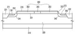
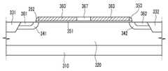
도 3은 본 발명의 다른 실시예에 따른 트랜지스터의 배치도이며, 도 4는 도 3의 트랜지스터를 Ⅳ-Ⅳ 선을 따라 자른 단면도이다.3 is a layout view of a transistor according to another exemplary embodiment of the present invention, and FIG. 4 is a cross-sectional view of the transistor of FIG. 3 taken along line IV-IV.
도 3을 참고하면, 본 실시예에 따른 트랜지스터 역시 기판(310) 위에 제1웰(320)이 형성되어 있으며, 제1웰(320)에는 소자 분리막(331, 332)이 형성되어 있 다. 소자 분리막(331, 332)은 활성 영역(321)을 정의하며, 소자 분리막(331, 332)과 활성 영역(321)이 접하는 부분에는 계면(edge)이 형성된다.Referring to FIG. 3, the
제1웰(320)에는 제2웰(341, 342)이 형성되어 있으며, 제2웰(341, 342)에는 소스/드레인 영역(361, 362)이 형성되어 있다. 제1웰(320) 위에는 게이트 절연막(351)이 형성되어 있으며, 게이트 절연막(351) 위에 게이트 전극(360)이 형성되어 있으며, 게이트 전극(360)은 제2웰(341, 342) 사이에 위치한다.
게이트 전극(360)은 활성 영역(121)과 중첩하며, 제1 부분(363), 제2 부분(364) 및 제3 부분(365)를 포함한다. 제1 부분(363)은 소스/드레인 영역(361, 362)에 도핑된 도전성 불순물과 동일한 도전형의 도전성 불순물로 도핑되어 있는 다결정 반도체이며, 제2 및 제3 부분(364, 365)은 제1웰(320)에 도핑된 도전성 불순물과 동일한 도전성 불순물로 도핑되어 있는 다결정 반도체이다. 제2 및 제3 부분(364, 365)은 활성 영역(321)의 계면 중 소스/드레인 영역(361, 362) 사이의 계면의 일부(322, 323)와 중첩한다. 본 실시예에 따르면, 소스/드레인 영역(361, 362) 사이에 형성되는 채널이 형성되는 경로 상에 존재하는 계면(322, 323)과 중첩하며, 제1웰(320)에 도핑된 도전성 불순물과 동일한 도전형을 갖는 도전성 불순물로 도핑되어 있는 제2 및 제3 부분(364, 365)를 형성함으로써 계면(322, 323)에서는 게이트 전극(360)이 트랜지스터의 한 단자로 역할을 못하게 한다. 따라서 계면(322, 323)에서는 채널이 형성되지 않아 험프 현상이 발생되는 것을 방지할 수 있다. The
게이트 전극(360)의 양 측면에는 스페이서(352)가 형성되어 있다.
게이트 전극(360), 소스/드레인 영역(361, 362) 위에는 각각 도전성 향상을위한 실리사이드층(370, 371, 372)이 형성되어 있다.Silicide layers 370, 371, and 372 are formed on the
소스/드레인 영역(361, 362)는 층간 절연막(도시하지 않음)을 통하여 소스/드레인 배선(도시하지 않음)과 연결되어 있을 수 있다.The source /
이제 도 5 내지 도 8을 참고하여 도 3 및 도 4에 도시한 트랜지스터의 제조 방법에 대하여 상세하게 설명한다.A method of manufacturing the transistors shown in FIGS. 3 and 4 will now be described in detail with reference to FIGS. 5 to 8.
도 5 내지 도 8은 각각 도 3 및 도 4에 도시한 트랜지스터를 제조하는 방법을 순서에 따라 도시한 단면도이다.5 through 8 are cross-sectional views sequentially illustrating a method of manufacturing the transistors shown in FIGS. 3 and 4, respectively.
먼저 도 5를 참고하면, 먼저 기판(310) 위에 예를 들어 p형 도전성 불순물이 도핑된 제1웰(320)을 형성하고, 제1웰(320)의 일부를 식각하고 식각된 부분에 절연물을 매립하여 소자 분리막(331, 332)을 형성하고, 제1웰(320)의 일부에 n형 도전성 불순물을 도핑하여 제2웰(341, 342)를 형성한다. 이어서 제1웰(320)위에 게이트 절연막(351)을 형성하고, 게이트 절연막(351) 위에 게이트 전극용 다결정 규소 패턴(367)을 형성하고, 게이트 전극용 다결정 규소 패턴(367)의 양 측면에 스페이서(352)를 형성한다.First, referring to FIG. 5, first, a
그런 후 감광막 패턴(510)을 형성하고, 감광막 패턴(510)을 마스크로 사용하여 제1웰(320)에 도핑된 도전성 불순물과 반대의 도전성 불순물, 예를 들어 n형 도전성 불순물을 도핑한다. 이때 도핑 농도는 제2웰(341, 342)의 도핑 농도보다 높다.Thereafter, the
그러면 도 6과 같이 n형 도전성 불순물을 도핑된 소스/드레인 영역(361, 362)이 형성되며, 게이트 전극용 다결정 규소 패턴(367) 중 일부가 n형 도전성 불순물로 도핑되어 게이트 전극(360)의 제1 부분(363)이 형성된다.Then, as shown in FIG. 6, source /
그런 후 도 7과 같이 도핑되지 않은 게이트 전극용 다결정 규소 패턴(367)을 노출하는 감광막 패턴(520)을 형성하고, 감광막 패턴(520)을 마스크로 사용하여 제1웰(320)에 도핑된 도전성 불순물과 동일한 도전성 불순물, 예를 들어 p형 도전성 불순물을 도핑한다.Then, as shown in FIG. 7, a
그러면 도 8과 같이 게이트 전극용 다결정 규소 패턴(367) 중 일부가 p형 도전성 불순물로 도핑되어 게이트 전극(360)의 제2 및 제3 부분(364, 365)이 형성된다.Then, as shown in FIG. 8, some of the
이어서 게이트 전극(360) 위에 절연막(370)을 형성하여 도 3 및 도 4와 같은 트랜지스터를 완성한다.Subsequently, an insulating
이제 도 9를 참고하여 본 발명의 한 실시예에 따른 트랜지스터의 성능에 대하여 상세하게 설명한다.A performance of a transistor according to an embodiment of the present invention will now be described in detail with reference to FIG. 9.
도 9는 종래 기술에 따른 트랜지스터 및 본 발명의 실시예에 따른 트랜지스터에서 게이트 전압(V)에 따른 드레인 전류(A)의 관계를 도시하는 그래프이다.9 is a graph showing the relationship between the drain current A according to the gate voltage V in the transistor according to the prior art and the transistor according to the embodiment of the present invention.
도 9를 참고하면, 종래 기술에 따른 트랜지스터는 포화 드레인 전류에 다다르기 전에 먼저 트랜지스터가 턴 온되어 도면에 원으로 표시한 바와 같이 험프 현상이 발생하는데 반하여 본 발명의 실시예에 따른 트랜지스터는 먼저 턴 온되는 현상 없이 포화 드레인 전류에 다다른다. 즉 본 발명에 따르면 소자 분리막과 활성 영역의 계면에서 채널이 형성되는 것을 방지하여 계면에서 발생하는 험프 현상이 제거된다.Referring to FIG. 9, a transistor according to the prior art first turns on before reaching a saturation drain current, and thus a hump phenomenon occurs as indicated by a circle in the drawing, whereas a transistor according to an embodiment of the present invention first turns on. Saturation drain current is reached without turning on. That is, according to the present invention, the hump phenomenon occurring at the interface is removed by preventing the formation of a channel at the interface between the device isolation layer and the active region.
이상에서 설명한 본 발명의 실시예는 장치 및 방법을 통해서만 구현이 되는 것은 아니며, 본 발명의 실시예의 구성에 대응하는 기능을 실현하는 프로그램 또는 그 프로그램이 기록된 기록 매체를 통해 구현될 수도 있다.The embodiments of the present invention described above are not only implemented through the apparatus and the method, but may be implemented through a program for realizing a function corresponding to the configuration of the embodiments of the present invention or a recording medium on which the program is recorded.
이상에서 본 발명의 실시예에 대하여 상세하게 설명하였지만 본 발명의 권리범위는 이에 한정되는 것은 아니고 다음의 청구범위에서 정의하고 있는 본 발명의 기본 개념을 이용한 당업자의 여러 변형 및 개량 형태 또한 본 발명의 권리범위에 속하는 것이다.Although the embodiments of the present invention have been described in detail above, the scope of the present invention is not limited thereto, and various modifications and improvements of those skilled in the art using the basic concepts of the present invention defined in the following claims are also provided. It belongs to the scope of rights.
도 1은 본 발명의 한 실시예에 따른 트랜지스터의 배치도이다.1 is a layout view of a transistor according to an embodiment of the present invention.
도 2는 도 1의 트랜지스터를 Ⅱ-Ⅱ 선을 따라 자른 단면도이다.FIG. 2 is a cross-sectional view of the transistor of FIG. 1 taken along line II-II. FIG.
도 3은 본 발명의 다른 실시예에 따른 트랜지스터의 배치도이다.3 is a layout view of a transistor according to another exemplary embodiment of the present invention.
도 4는 도 3의 트랜지스터를 Ⅳ-Ⅳ 선을 따라 자른 단면도이다.4 is a cross-sectional view of the transistor of FIG. 3 taken along line IV-IV.
도 5 내지 도 8은 각각 도 3 및 도 4에 도시한 트랜지스터를 제조하는 방법을 순서에 따라 도시한 단면도이다.5 through 8 are cross-sectional views sequentially illustrating a method of manufacturing the transistors shown in FIGS. 3 and 4, respectively.
도 9는 종래 기술에 따른 트랜지스터 및 본 발명의 실시예에 따른 트랜지스터에서 게이트 전압에 따른 드레인 전류의 관계를 도시하는 그래프이다.9 is a graph showing the relationship between the drain current according to the gate voltage in the transistor according to the prior art and the transistor according to the embodiment of the present invention.
Claims (16)
Translated fromKoreanPriority Applications (1)
| Application Number | Priority Date | Filing Date | Title |
|---|---|---|---|
| KR1020090059395AKR101034670B1 (en) | 2009-06-30 | 2009-06-30 | Transistors and manufacturing method thereof |
Applications Claiming Priority (1)
| Application Number | Priority Date | Filing Date | Title |
|---|---|---|---|
| KR1020090059395AKR101034670B1 (en) | 2009-06-30 | 2009-06-30 | Transistors and manufacturing method thereof |
Publications (2)
| Publication Number | Publication Date |
|---|---|
| KR20110001729A KR20110001729A (en) | 2011-01-06 |
| KR101034670B1true KR101034670B1 (en) | 2011-05-16 |
Family
ID=43610259
Family Applications (1)
| Application Number | Title | Priority Date | Filing Date |
|---|---|---|---|
| KR1020090059395AExpired - Fee RelatedKR101034670B1 (en) | 2009-06-30 | 2009-06-30 | Transistors and manufacturing method thereof |
Country Status (1)
| Country | Link |
|---|---|
| KR (1) | KR101034670B1 (en) |
Families Citing this family (1)
| Publication number | Priority date | Publication date | Assignee | Title |
|---|---|---|---|---|
| KR20120124788A (en)* | 2011-05-04 | 2012-11-14 | 삼성전자주식회사 | Semiconductor device |
Citations (3)
| Publication number | Priority date | Publication date | Assignee | Title |
|---|---|---|---|---|
| JP2001156290A (en)* | 1999-11-30 | 2001-06-08 | Nec Corp | Semiconductor device |
| KR20090010330A (en)* | 2007-07-23 | 2009-01-30 | 삼성전자주식회사 | Semiconductor device and manufacturing method thereof |
| KR20090025405A (en)* | 2007-09-06 | 2009-03-11 | 주식회사 하이닉스반도체 | Manufacturing method of semiconductor device |
- 2009
- 2009-06-30KRKR1020090059395Apatent/KR101034670B1/ennot_activeExpired - Fee Related
Patent Citations (3)
| Publication number | Priority date | Publication date | Assignee | Title |
|---|---|---|---|---|
| JP2001156290A (en)* | 1999-11-30 | 2001-06-08 | Nec Corp | Semiconductor device |
| KR20090010330A (en)* | 2007-07-23 | 2009-01-30 | 삼성전자주식회사 | Semiconductor device and manufacturing method thereof |
| KR20090025405A (en)* | 2007-09-06 | 2009-03-11 | 주식회사 하이닉스반도체 | Manufacturing method of semiconductor device |
Also Published As
| Publication number | Publication date |
|---|---|
| KR20110001729A (en) | 2011-01-06 |
Similar Documents
| Publication | Publication Date | Title |
|---|---|---|
| US8722522B2 (en) | Electro-static discharge protection device, semiconductor device, and method for manufacturing electro-static discharge protection device | |
| US7902600B2 (en) | Metal oxide semiconductor device | |
| CN101800228B (en) | Semiconductor device | |
| KR101413651B1 (en) | Semiconductor device having transistor and method for manufacturing the same | |
| US6919606B2 (en) | Semiconductor device comprising an insulating mask formed on parts of a gate electrode and semiconductor layer crossing an active region | |
| JP4104701B2 (en) | Semiconductor device | |
| JP2012160510A (en) | Semiconductor device and method of manufacturing the same | |
| US9196719B2 (en) | ESD protection circuit | |
| JP5535486B2 (en) | Method and apparatus for forming body contact element having structure (SOI) in which semiconductor is provided on insulator | |
| US20230137101A1 (en) | Integrated Circuit Structure of N-Type and P-Type FinFET Transistors | |
| US7196375B2 (en) | High-voltage MOS transistor | |
| US20070278613A1 (en) | Semiconductor device | |
| US7485925B2 (en) | High voltage metal oxide semiconductor transistor and fabricating method thereof | |
| US7994584B2 (en) | Semiconductor device having non-silicide region in which no silicide is formed on diffusion layer | |
| CN101373769B (en) | Semiconductor device | |
| CN101373767A (en) | Semiconductor device | |
| JP5211132B2 (en) | Semiconductor device | |
| CN101364596A (en) | Semiconductor device | |
| KR101034670B1 (en) | Transistors and manufacturing method thereof | |
| US9196751B2 (en) | Junction FET semiconductor device with dummy mask structures for improved dimension control and method for forming the same | |
| KR100290900B1 (en) | Manufacturing method of transistor for electrostatic protection | |
| JP5511353B2 (en) | Semiconductor device | |
| JP5092313B2 (en) | Manufacturing method of semiconductor device | |
| JP5434501B2 (en) | MOS transistor, semiconductor integrated circuit device, semiconductor device | |
| JP4344390B2 (en) | Semiconductor device |
Legal Events
| Date | Code | Title | Description |
|---|---|---|---|
| A201 | Request for examination | ||
| PA0109 | Patent application | St.27 status event code:A-0-1-A10-A12-nap-PA0109 | |
| PA0201 | Request for examination | St.27 status event code:A-1-2-D10-D11-exm-PA0201 | |
| D13-X000 | Search requested | St.27 status event code:A-1-2-D10-D13-srh-X000 | |
| D14-X000 | Search report completed | St.27 status event code:A-1-2-D10-D14-srh-X000 | |
| E902 | Notification of reason for refusal | ||
| PE0902 | Notice of grounds for rejection | St.27 status event code:A-1-2-D10-D21-exm-PE0902 | |
| PG1501 | Laying open of application | St.27 status event code:A-1-1-Q10-Q12-nap-PG1501 | |
| T11-X000 | Administrative time limit extension requested | St.27 status event code:U-3-3-T10-T11-oth-X000 | |
| E13-X000 | Pre-grant limitation requested | St.27 status event code:A-2-3-E10-E13-lim-X000 | |
| P11-X000 | Amendment of application requested | St.27 status event code:A-2-2-P10-P11-nap-X000 | |
| P13-X000 | Application amended | St.27 status event code:A-2-2-P10-P13-nap-X000 | |
| E701 | Decision to grant or registration of patent right | ||
| PE0701 | Decision of registration | St.27 status event code:A-1-2-D10-D22-exm-PE0701 | |
| GRNT | Written decision to grant | ||
| PR0701 | Registration of establishment | St.27 status event code:A-2-4-F10-F11-exm-PR0701 | |
| PR1002 | Payment of registration fee | St.27 status event code:A-2-2-U10-U11-oth-PR1002 Fee payment year number:1 | |
| PG1601 | Publication of registration | St.27 status event code:A-4-4-Q10-Q13-nap-PG1601 | |
| LAPS | Lapse due to unpaid annual fee | ||
| PC1903 | Unpaid annual fee | St.27 status event code:A-4-4-U10-U13-oth-PC1903 Not in force date:20140505 Payment event data comment text:Termination Category : DEFAULT_OF_REGISTRATION_FEE | |
| PN2301 | Change of applicant | St.27 status event code:A-5-5-R10-R11-asn-PN2301 | |
| PC1903 | Unpaid annual fee | St.27 status event code:N-4-6-H10-H13-oth-PC1903 Ip right cessation event data comment text:Termination Category : DEFAULT_OF_REGISTRATION_FEE Not in force date:20140505 | |
| P22-X000 | Classification modified | St.27 status event code:A-4-4-P10-P22-nap-X000 |