KR101028901B1 - Memory Devices, Memory Management Devices, and Memory Management Methods - Google Patents
Memory Devices, Memory Management Devices, and Memory Management MethodsDownload PDFInfo
- Publication number
- KR101028901B1 KR101028901B1KR1020090009229AKR20090009229AKR101028901B1KR 101028901 B1KR101028901 B1KR 101028901B1KR 1020090009229 AKR1020090009229 AKR 1020090009229AKR 20090009229 AKR20090009229 AKR 20090009229AKR 101028901 B1KR101028901 B1KR 101028901B1
- Authority
- KR
- South Korea
- Prior art keywords
- memory
- information
- data
- inspection
- data pattern
- Prior art date
- Legal status (The legal status is an assumption and is not a legal conclusion. Google has not performed a legal analysis and makes no representation as to the accuracy of the status listed.)
- Expired - Fee Related
Links
Images


Classifications
- G—PHYSICS
- G11—INFORMATION STORAGE
- G11C—STATIC STORES
- G11C29/00—Checking stores for correct operation ; Subsequent repair; Testing stores during standby or offline operation
- G—PHYSICS
- G11—INFORMATION STORAGE
- G11C—STATIC STORES
- G11C29/00—Checking stores for correct operation ; Subsequent repair; Testing stores during standby or offline operation
- G11C29/04—Detection or location of defective memory elements, e.g. cell constructio details, timing of test signals
- G11C29/08—Functional testing, e.g. testing during refresh, power-on self testing [POST] or distributed testing
- G—PHYSICS
- G01—MEASURING; TESTING
- G01R—MEASURING ELECTRIC VARIABLES; MEASURING MAGNETIC VARIABLES
- G01R31/00—Arrangements for testing electric properties; Arrangements for locating electric faults; Arrangements for electrical testing characterised by what is being tested not provided for elsewhere
- G01R31/28—Testing of electronic circuits, e.g. by signal tracer
- G—PHYSICS
- G06—COMPUTING OR CALCULATING; COUNTING
- G06F—ELECTRIC DIGITAL DATA PROCESSING
- G06F11/00—Error detection; Error correction; Monitoring
- G06F11/07—Responding to the occurrence of a fault, e.g. fault tolerance
- G06F11/08—Error detection or correction by redundancy in data representation, e.g. by using checking codes
- G—PHYSICS
- G06—COMPUTING OR CALCULATING; COUNTING
- G06F—ELECTRIC DIGITAL DATA PROCESSING
- G06F30/00—Computer-aided design [CAD]
- G06F30/30—Circuit design
- G06F30/32—Circuit design at the digital level
- G06F30/33—Design verification, e.g. functional simulation or model checking
- G—PHYSICS
- G11—INFORMATION STORAGE
- G11C—STATIC STORES
- G11C16/00—Erasable programmable read-only memories
- G11C16/02—Erasable programmable read-only memories electrically programmable
- G11C16/06—Auxiliary circuits, e.g. for writing into memory
- G11C16/34—Determination of programming status, e.g. threshold voltage, overprogramming or underprogramming, retention
- G11C16/349—Arrangements for evaluating degradation, retention or wearout, e.g. by counting erase cycles
- G—PHYSICS
- G11—INFORMATION STORAGE
- G11C—STATIC STORES
- G11C29/00—Checking stores for correct operation ; Subsequent repair; Testing stores during standby or offline operation
- G11C29/04—Detection or location of defective memory elements, e.g. cell constructio details, timing of test signals
- G11C29/08—Functional testing, e.g. testing during refresh, power-on self testing [POST] or distributed testing
- G11C29/12—Built-in arrangements for testing, e.g. built-in self testing [BIST] or interconnection details
- G—PHYSICS
- G11—INFORMATION STORAGE
- G11C—STATIC STORES
- G11C16/00—Erasable programmable read-only memories
- G11C16/02—Erasable programmable read-only memories electrically programmable
- G11C16/04—Erasable programmable read-only memories electrically programmable using variable threshold transistors, e.g. FAMOS
Landscapes
- Engineering & Computer Science (AREA)
- Physics & Mathematics (AREA)
- Theoretical Computer Science (AREA)
- General Engineering & Computer Science (AREA)
- General Physics & Mathematics (AREA)
- Computer Hardware Design (AREA)
- Evolutionary Computation (AREA)
- Geometry (AREA)
- Quality & Reliability (AREA)
- Techniques For Improving Reliability Of Storages (AREA)
- For Increasing The Reliability Of Semiconductor Memories (AREA)
Abstract
Translated fromKoreanDescription
Translated fromKorean메모리 장치와 메모리 관리 장치 및 메모리 관리 방법이 개시된다. 특히, 시스템 성능의 저하 없이, 메모리에 기록되어 있는 데이터의 패턴(pattern)을 검사(check)할 수 있는 메모리 장치와 메모리 관리 장치 및 메모리 관리 방법이 개시된다.A memory device, a memory management device, and a memory management method are disclosed. In particular, a memory device, a memory management device, and a memory management method capable of checking a pattern of data recorded in a memory without degrading system performance are disclosed.
데이터를 저장하는 스토리지 장치로는 자기 디스크(magnetic disk), 반도체 메모리 등이 있을 수 있다. 스토리지 장치는 종류 별로 서로 다른 물리적 특성을 가지기 때문에 물리적 특성에 상응하는 관리 방법이 필요하다.Storage devices for storing data may include magnetic disks and semiconductor memories. Since storage devices have different physical characteristics by type, a management method corresponding to the physical characteristics is required.
종래의 스토리지 장치로는 자기 디스크가 널리 사용되어 왔다. 자기 디스크는 평균적으로 킬로바이트(kilobyte) 당 수 밀리초(millisecond)의 읽기 및 쓰기 시간을 특성으로 가진다. 또한, 자기 디스크는 데이터가 저장된 물리적 위치에 따라 암(arm)이 도달하는 시간이 다르기 때문에 읽기 및 쓰기 시간이 달라지는 특성을 가진다.Magnetic disks have been widely used as a conventional storage device. Magnetic disks, on average, feature read and write times of a few milliseconds per kilobyte. In addition, the magnetic disk has a characteristic that the read and write time is different because the time that the arm arrives varies depending on the physical location where the data is stored.
최근에는 자기 디스크에 비하여 읽기 및 쓰기 시간이 짧고 작은 전력을 소모 하며 작은 부피를 차지하는 비휘발성(non-volatile) 메모리가 급속하게 자기 디스크를 대체하고 있다. 이는 비휘발성 메모리의 대용량화가 이루어졌기 때문에 가능한 결과이다.Recently, non-volatile memory, which consumes less power and consumes less power than the magnetic disk, is rapidly replacing magnetic disk. This is possible because of the large capacity of the nonvolatile memory.
비휘발성 메모리는 전기적으로 읽기(read), 쓰기(write) 및 소거(erase)가 가능하며, 공급 전원이 없는 상태에서도 저장된 데이터를 유지할 수 있는 반도체 메모리 장치이다. 비휘발성 메모리 장치에 대한 데이터의 저장 과정은 쓰기 외에도 프로그래밍(programming)이라고 불리기도 한다.A nonvolatile memory is a semiconductor memory device capable of electrically reading, writing, and erasing and maintaining stored data even without a power supply. In addition to writing, the process of storing data for nonvolatile memory devices is also called programming.
비휘발성 메모리의 대표적인 것으로 플래시(Flash) 메모리를 들 수 있으며, 플래시 메모리는 종래의 하드 디스크 드라이브(Hard Disk Drive, HDD)에 비하면 크기가 작고, 전력 소모량이 작으며, 읽기 속도를 높일 수 있는 이점이 있다. 최근에는 대용량의 플래시 메모리를 이용하여 HDD를 대체하기 위한 SSD(Solid State Disk)가 제안되기도 하였다.Flash memory is a representative example of non-volatile memory, which is smaller in size, smaller in power consumption, and faster in reading compared to a conventional hard disk drive (HDD). There is this. Recently, a solid state disk (SSD) has been proposed to replace an HDD by using a large flash memory.
플래시 메모리의 종류로서 대표적인 것들로는 NAND 방식의 플래시 메모리와 NOR 플래시 메모리 등을 들 수 있다. NAND 방식과 NOR 방식은 셀 어레이의 구성 및 동작 방식에 의해 구별될 수 있다.Representative types of flash memory include NAND flash memory and NOR flash memory. The NAND method and the NOR method may be distinguished by a configuration and an operation method of a cell array.
플래시 메모리는 다수의 메모리 셀들의 배열로 이루어지며, 하나의 메모리 셀은 하나 이상의 데이터 비트를 저장할 수 있다. 하나의 메모리 셀은 컨트롤 게이트(control gate) 및 플로팅 게이트(floating gate)를 포함하며, 컨트롤 게이트 및 플로팅 게이트 사이에는 절연체(insulator)가 삽입되고, 플로팅 게이트 및 서브스트레이트(substrate) 간에도 절연체가 삽입된다.Flash memory consists of an array of multiple memory cells, where one memory cell can store one or more data bits. One memory cell includes a control gate and a floating gate, and an insulator is inserted between the control gate and the floating gate, and an insulator is inserted between the floating gate and the substrate. .
이러한 비휘발성 메모리는 소정의 컨트롤러에 의해 관리가 이루어진다. 그리고, 이러한 컨트롤러의 성능에 따라 비휘발성 메모리 전체의 성능이 결정될 수도 있다.Such a nonvolatile memory is managed by a predetermined controller. In addition, the performance of the entire nonvolatile memory may be determined according to the performance of the controller.
따라서, 메모리를 효율적으로 관리 및 제어할 수 있는 방안에 대한 연구가 필요하다.Therefore, there is a need for a study on how to manage and control the memory efficiently.
CPU가 램(RAM)에 대한 접근 없이, 메모리의 소정 영역에 기록되어 있는 데이터의 패턴(pattern)을 검사(check)할 수 있는 메모리 장치, 메모리 관리 장치 및 메모리 관리 방법을 개시함으로써, 데이터 패턴 검사시 발생할 수 있는 시스템 성능 저하를 방지할 수 있도록 한다.Data pattern checking by initiating a memory device, a memory management device, and a memory management method in which a CPU can check a pattern of data recorded in a predetermined area of a memory without accessing a RAM This can prevent the system performance degradation that may occur.
본 발명의 일실시예에 따른 메모리 장치는 CPU(Central Processing Unit)로부터 검사(check) 명령 및 검사 정보를 수신하는 수신부, 상기 검사 명령에 대응하여 상기 검사 정보를 기초로 메모리의 소정 영역에 기록(write)되어 있는 데이터를 독출(read)하는 독출부 및 상기 검사 정보를 기초로 상기 독출된 데이터의 데이터 패턴(pattern)을 검사하는 검사부를 포함한다.According to an embodiment of the present invention, a memory device includes a receiver configured to receive a check command and inspection information from a central processing unit (CPU), and write a predetermined area of the memory based on the inspection information in response to the inspection command ( and a reading unit that reads data that has been written, and an inspection unit that examines a data pattern of the read data based on the inspection information.
또한, 본 발명의 일실시예에 따른 메모리 관리 장치는 CPU(Central Processing Unit)에 의해 검사(check) 명령 및 검사 정보가 기록(read)되는 제어 레지스터(register), 상기 제어 레지스터에 상기 검사 명령 및 검사 정보가 기록되면, 상기 검사 명령에 대응하여 상기 검사 정보를 기초로 메모리의 소정 영역에 기록되어 있는 데이터를 독출(read)하는 독출부, 상기 검사 정보를 기초로 상기 독출된 데이터의 데이터 패턴(pattern)을 검사하는 검사부 및 상기 검사부의 검사 결과가 기록되는 상태 레지스터를 포함한다.In addition, the memory management apparatus according to an embodiment of the present invention includes a control register in which a check instruction and inspection information are read by a central processing unit (CPU), the check instruction in the control register and A reading unit for reading data recorded in a predetermined area of a memory based on the inspection information in response to the inspection command when the inspection information is recorded, and a data pattern of the read data based on the inspection information ( and a status register in which the test result of the test part is recorded.
또한, 본 발명의 일실시예에 따른 메모리 관리 방법은 CPU(Central Processing Unit)로부터 검사(check) 명령 및 검사 정보를 수신하는 단계, 상기 검사 명령에 대응하여 상기 검사 정보를 기초로 메모리의 소정 영역에 기록(write)되어 있는 데이터를 독출(read)하는 단계 및 상기 검사 정보를 기초로 상기 독출된 데이터의 데이터 패턴(pattern)을 검사하는 단계를 포함한다.The memory management method may further include receiving a check command and check information from a central processing unit (CPU), and a predetermined area of the memory based on the check information in response to the check command. Reading the data written to the data, and examining a data pattern of the read data based on the inspection information.
CPU가 램(RAM)에 대한 접근 없이, 메모리의 소정 영역에 기록되어 있는 데이터의 패턴(pattern)을 검사(check)할 수 있는 메모리 장치, 메모리 관리 장치 및 메모리 관리 방법을 개시함으로써, 데이터 패턴 검사시 발생할 수 있는 시스템 성능 저하를 방지할 수 있다.Data pattern checking by initiating a memory device, a memory management device, and a memory management method in which a CPU can check a pattern of data recorded in a predetermined area of a memory without accessing a RAM This can prevent system performance degradation that may occur.
이하에서, 첨부된 도면을 참조하여 본 발명에 따른 실시예들을 상세히 설명한다. 그러나, 본 발명이 실시예들에 의해 제한되거나 한정되는 것은 아니다. 또한, 각 도면에 제시된 동일한 참조 부호는 동일한 부재를 나타낸다.Hereinafter, with reference to the accompanying drawings will be described embodiments of the present invention; However, the present invention is not limited or limited by the embodiments. Also, like reference numerals in the drawings denote like elements.
일반적으로 비휘발성 메모리에 대한 프로그래밍(programming)은 페이지(page) 단위로 수행될 수 있고 소거(erase)는 블록(block) 단위로 수행될 수 있다. 이때, 블록은 복수의 페이지들을 포함할 수 있다.In general, programming of the nonvolatile memory may be performed in units of pages, and erasing may be performed in units of blocks. In this case, the block may include a plurality of pages.
또한, 비휘발성 메모리를 관리하는 메모리 컨트롤러는 외부의 호스트(host) 또는 프로세서(processor)에 논리 주소(logical address)를 제공하고, 비휘발성 메모리에 대해 물리 주소(physical address)를 제공할 수 있다.In addition, the memory controller managing the nonvolatile memory may provide a logical address to an external host or processor and may provide a physical address to the nonvolatile memory.
이때, 메모리 컨트롤러는 물리 주소를 이용하여 비휘발성 메모리를 관리하 고, 물리 주소를 논리 주소로 변환할 수 있다.In this case, the memory controller may manage the nonvolatile memory using a physical address and convert the physical address into a logical address.
여기서, 물리 주소 및 논리 주소의 변환이 수행되는 계층을 플래시 변환 계층(Flash Translation Layer: FTL)이라 하기도 한다.Here, the layer in which the physical address and logical address translation is performed may be referred to as a flash translation layer (FTL).
비휘발성 메모리의 대표적인 것으로 플래시(flash) 메모리를 들 수 있는데, 이러한 플래시 메모리는 대표적으로 NAND 방식의 플래시 메모리와 NOR 방식의 플래시 메모리 등으로 나뉠 수 있다.A flash memory is a representative example of a nonvolatile memory. Such flash memory may be classified into a NAND flash memory and a NOR flash memory.
NAND 방식의 플래시 메모리는 NOR 방식의 플래시 메모리에 비해 집적도가 높고 용량 대 가격비가 높기 때문에 비휘발성 메모리로 많이 사용되고 있지만, NOR 방식의 플래시 메모리와는 달리 랜덤 억세스(Random Access)가 불가능하다.NAND flash memory is widely used as a nonvolatile memory because of its higher density and higher cost-to-price ratio than NOR flash memory. However, unlike NOR flash memory, random access is not possible.
따라서, NAND 방식의 플래시 메모리의 특정 영역에 기록되어 있는 데이터의 패턴(pattern)을 검사(check)하기 위해서는 상기 특정 영역의 내용을 램(RAM)으로 읽어(read) 들인 후 램에 복사된 내용을 검사하는 방법을 사용해야 한다.Therefore, in order to check a pattern of data recorded in a specific region of a NAND flash memory, the contents of the specific region are read into a RAM, and the contents copied into the RAM are read. You should use a method of testing.
이 경우, 메모리로부터 램으로 데이터를 읽어 들이는 과정과 데이터 내용을 검사하기 위해 CPU(Central Processing Unit)가 램으로 접근하는 과정이 수반되기 때문에 두 번에 걸친 메모리 버스(bus) 접근이 필요해져서 전반적인 시스템 성능 저하가 발생할 수 있다.In this case, the process involves reading data from memory into RAM and accessing RAM by the Central Processing Unit (CPU) to examine the data contents. System degradation may occur.
따라서, 본 발명의 일실시예에 따른 메모리 장치 및 메모리 관리 장치는 CPU로부터 선정된(predetermined) 데이터 패턴을 전달받아, 메모리의 특정 영역에 기록되어 있는 데이터의 패턴과 상기 선정된 데이터 패턴을 비교하여 상기 메모리의 특정 영역에 기록되어 있는 데이터의 패턴을 검사함으로써, CPU 및 메모리 버스의 점유에 따른 시스템 성능 저하를 방지할 수 있다.Therefore, the memory device and the memory management device according to an embodiment of the present invention receive a predetermined data pattern from the CPU, and compare the pattern of data recorded in a specific area of the memory with the selected data pattern. By inspecting the pattern of data recorded in the specific area of the memory, it is possible to prevent a decrease in system performance due to the occupation of the CPU and the memory bus.
따라서, 이하에서는 도 1 및 도 2를 참조하여 본 발명의 일실시예에 따른 메모리 장치 및 메모리 관리 장치에 대해 상세히 설명하기로 한다.Therefore, hereinafter, a memory device and a memory management device according to an embodiment of the present invention will be described in detail with reference to FIGS. 1 and 2.
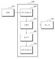
도 1은 본 발명의 일실시예에 따른 메모리 장치의 구조를 도시한 도면이다.1 is a diagram illustrating a structure of a memory device according to an embodiment of the present invention.
도 1을 참조하면, CPU(110), 메모리 장치(120)가 도시되어 있다.Referring to FIG. 1, a
메모리 장치(120)는 수신부(121), 독출부(122), 검사부(123)를 포함할 수 있다.The
본 발명의 일실시예에 따르면, 메모리(124)는 NAND 방식의 플래시 메모리일 수 있다.According to an embodiment of the present invention, the
수신부(121)는 CPU(110)로부터 검사(check) 명령 및 검사 정보를 수신한다.The
독출부(122)는 수신부(121)가 수신한 상기 검사 명령에 대응하여 상기 검사 정보를 기초로 메모리(124)의 소정 영역에 기록되어 있는 데이터를 독출(read)한다.The read
본 발명의 일실시예에 따르면, 상기 검사 정보는 메모리 영역 정보를 포함할 수 있다.According to an embodiment of the present invention, the inspection information may include memory area information.
이때, 본 발명의 일실시예에 따르면, 상기 메모리 영역 정보는 메모리(124)의 소정 영역에 대한 시작 주소 정보 및 크기 정보를 포함할 수 있다.In this case, according to an embodiment of the present invention, the memory area information may include start address information and size information of a predetermined area of the
이때, 본 발명의 일실시예에 따르면, 독출부(122)는 상기 메모리 영역 정보에 기초하여 메모리(124)의 소정 영역에 기록되어 있는 상기 데이터를 독출할 수 있다.At this time, according to an embodiment of the present invention, the read
즉, 수신부(121)가 CPU(110)로부터 메모리(124)의 소정 영역에 대한 시작 주소 정보 및 크기 정보 등을 수신하면, 독출부(122)는 상기 시작 주소 정보 및 크기 정보를 이용하여 메모리(124)의 소정 영역으로부터 데이터를 독출할 수 있다.That is, when the
검사부(123)는 상기 검사 정보를 기초로 독출부(122)가 독출한 데이터의 데이터 패턴을 검사한다.The
본 발명의 일실시예에 따르면, 상기 검사 정보는 선정된(predetermined) 데이터 패턴에 대한 정보를 포함할 수 있다.According to an embodiment of the present invention, the inspection information may include information about a predetermined data pattern.
이때, 본 발명의 일실시예에 따르면, 검사부(123)는 상기 선정된 데이터 패턴과 상기 독출된 데이터의 데이터 패턴을 비교하여 상기 선정된 데이터 패턴과 상기 독출된 데이터의 데이터 패턴이 서로 일치하는지 여부를 판단할 수 있다.At this time, according to an embodiment of the present invention, the
만약, 상기 선정된 데이터 패턴과 상기 독출된 데이터의 데이터 패턴이 서로 일치하지 않는 경우, 검사부(123)는 에러(error) 메시지를 생성할 수 있다.If the selected data pattern and the data pattern of the read data do not coincide with each other, the
예컨대, CPU(110)가 메모리(124)의 소정 영역에 기록되어 있는 데이터가 "1234567b" 라는 값과 일치하는지 여부를 검사하려고 하는 경우, CPU(110)는 메모리 장치(120)로 "1234567b" 라는 데이터 패턴에 대한 정보를 전송할 수 있다.For example, when the
그리고, 검사부(123)는 독출부(122)가 독출한 데이터의 데이터 패턴과 "1234567b" 라는 데이터 패턴이 서로 일치하는지 여부를 판단하고, 만약, 상기 두 데이터 패턴이 서로 일치하지 않는 경우, 에러를 발생시킬 수 있다.The
본 발명의 일실시예에 따르면, 메모리 장치(120)는 검사부(123)가 데이터 패턴의 검사를 종료하는 경우, 상기 독출된 데이터를 램에 저장하지 않고, 폐기할 수 있다.According to an exemplary embodiment of the present disclosure, when the
결국, 본 발명의 일실시예에 따른 메모리 장치(120)는 CPU가 메모리(124)에 기록되어 있는 데이터의 패턴을 검사하고자 하는 경우, 램에 대한 접근 없이, 메모리 장치(120) 내에 포함되어 있는 수신부(121), 독출부(122) 및 검사부(123)를 통해 데이터 패턴의 검사가 가능하도록 함으로써, 기존의 램을 이용하여 데이터 패턴을 검사하는 경우와는 달리, 전반적인 시스템 성능 저하를 방지할 수 있다.As a result, the
이상, 도 1을 참조하여 본 발명의 일실시예에 따른 메모리 장치(120)에 대해 설명하였다.The
본 발명의 일실시예에 따르면, 데이터 패턴의 검사를 수행하기 위한 본 발명의 기본 아이디어는 도 1에 도시된 바와 같이, 메모리 장치(120) 내부에 소정의 기능을 수행하는 구성을 포함함으로써 구체화될 수도 있고, 메모리 장치(120)와는 별도로 메모리 장치(120)에 연결될 수 있는 소정의 메모리 관리 장치로 구체화될 수도 있다.According to one embodiment of the present invention, the basic idea of the present invention for performing the inspection of the data pattern may be embodied by including a configuration for performing a predetermined function inside the
따라서, 이하에서는 도 2를 참조하여 본 발명의 일실시예에 따른 메모리 관리 장치에 대해 상세히 설명하기로 한다.Therefore, hereinafter, a memory management apparatus according to an exemplary embodiment of the present invention will be described in detail with reference to FIG. 2.
도 2는 본 발명의 일실시예에 따른 메모리 관리 장치의 구조를 도시한 도면이다.2 is a diagram illustrating a structure of a memory management apparatus according to an embodiment of the present invention.
도 2를 참조하면, CPU(210), 메모리 관리 장치(220) 및 메모리(230)가 도시되어 있다.Referring to FIG. 2, a
메모리 관리 장치(220)는 제어 레지스터(register)(221), 독출부(222), 검사 부(223) 및 상태 레지스터(224)를 포함할 수 있다.The
본 발명의 일실시예에 따르면, 메모리(230)는 NAND 방식의 플래시 메모리일 수 있다.According to an embodiment of the present invention, the
제어 레지스터(221)는 CPU(210)에 의해 검사 명령 및 검사 정보가 기록된다.The control register 221 records the inspection command and inspection information by the
독출부(222)는 제어 레지스터(221)에 상기 검사 명령 및 검사 정보가 기록되면, 상기 검사 명령에 대응하여 상기 검사 정보를 기초로 메모리(230)의 소정 영역에 기록되어 있는 데이터를 독출한다.When the inspection command and inspection information are recorded in the
본 발명의 일실시예에 따르면, 상기 검사 정보는 메모리 영역 정보를 포함할 수 있다.According to an embodiment of the present invention, the inspection information may include memory area information.
이때, 본 발명의 일실시예에 따르면, 상기 메모리 영역 정보는 메모리(230)의 소정 영역에 대한 시작 주소 정보 및 크기 정보를 포함할 수 있다.In this case, according to an embodiment of the present invention, the memory area information may include start address information and size information of a predetermined area of the
이때, 본 발명의 일실시예에 따르면, 독출부(222)는 상기 메모리 영역 정보에 기초하여 메모리(230)의 소정 영역에 기록되어 있는 상기 데이터를 독출할 수 있다.At this time, according to an embodiment of the present invention, the
즉, CPU(210)가 제어 레지스터(221)에 메모리(230)의 소정 영역에 대한 시작 주소 정보 및 크기 정보 등을 기록하면, 독출부(222)는 상기 시작 주소 정보 및 크기 정보를 이용하여 메모리(230)의 소정 영역으로부터 데이터를 독출할 수 있다.That is, when the
검사부(223)는 상기 검사 정보를 기초로 독출부(222)가 독출한 데이터의 데이터 패턴을 검사한다.The
상태 레지스터(224)는 검사부(223)의 검사 결과가 기록된다.The status register 224 records the test result of the
본 발명의 일실시예에 따르면, 상기 검사 정보는 선정된 데이터 패턴에 대한 정보를 포함할 수 있다.According to an embodiment of the present invention, the inspection information may include information on the selected data pattern.
이때, 본 발명의 일실시예에 따르면, 검사부(223)는 상기 선정된 데이터 패턴과 상기 독출된 데이터의 데이터 패턴을 비교하여 상기 선정된 데이터 패턴과 상기 독출된 데이터의 데이터 패턴이 서로 일치하는지 여부를 판단할 수 있다.At this time, according to an embodiment of the present invention, the
만약, 상기 선정된 데이터 패턴과 상기 독출된 데이터의 데이터 패턴이 서로 일치하지 않는 경우, 검사부(223)는 에러 메시지를 생성하고, 상기 에러 메시지를 상태 레지스터(224)에 기록할 수 있다.If the selected data pattern and the data pattern of the read data do not coincide with each other, the
예컨대, CPU(210)가 메모리(230)의 소정 영역에 기록되어 있는 데이터가 "1234567b" 라는 값과 일치하는지 여부를 검사하려고 하는 경우, CPU(210)는 제어 레지스터(221)에 "1234567b" 라는 데이터 패턴에 대한 정보를 기록할 수 있다.For example, when the
그리고, 검사부(223)는 독출부(222)가 독출한 데이터의 데이터 패턴이 "1234567b" 라는 데이터 패턴과 일치하는지 여부를 판단하고, 만약, 상기 두 데이터 패턴이 서로 일치하지 않는 경우, 에러를 발생시킬 수 있다.The
그리고 나서, 검사부(223)는 상기 미스매치(MISMATCH) 에러가 발생하였음을 상태 레지스터(224)에 표시할 수 있다.Then, the inspecting
결국, CPU(210)는 상태 레지스터(224)를 통해 메모리(230)의 소정 영역에 기록되어 있는 데이터의 패턴이 잘못되었음을 판단할 수 있다.As a result, the
본 발명의 일실시예에 따르면, 메모리 관리 장치(220)는 검사부(223)가 데이터 패턴의 검사를 종료하는 경우, 상기 독출된 데이터를 램에 저장하지 않고, 폐기 할 수 있다.According to an embodiment of the present disclosure, when the
결국, 본 발명의 일실시예에 따른 메모리 관리 장치(220)는 CPU(210)가 메모리(230)에 기록되어 있는 데이터의 패턴을 검사하고자 하는 경우, 램에 대한 접근 없이, 메모리 관리 장치(220)를 통해 데이터 패턴의 검사가 가능하도록 함으로써, 기존의 램을 이용하여 데이터 패턴을 검사하는 경우와는 달리, 전반적인 시스템 성능 저하를 방지할 수 있다.As a result, the
도 3은 본 발명의 일실시예에 따른 메모리 관리 방법을 도시한 순서도이다.3 is a flowchart illustrating a memory management method according to an embodiment of the present invention.
단계(S310)에서는 CPU로부터 검사 명령 및 검사 정보를 수신한다.In step S310, an inspection command and inspection information are received from the CPU.
단계(S320)에서는 상기 검사 명령에 대응하여 상기 검사 정보를 기초로 메모리의 소정 영역에 기록되어 있는 데이터를 독출한다.In operation S320, data recorded in a predetermined area of the memory is read based on the inspection information in response to the inspection command.
본 발명의 일실시예에 따르면, 상기 검사 정보는 메모리 영역 정보를 포함할 수 있다.According to an embodiment of the present invention, the inspection information may include memory area information.
이때, 본 발명의 일실시예에 따르면, 상기 메모리 영역 정보는 상기 메모리의 소정 영역에 대한 시작 주소 정보 및 크기 정보를 포함할 수 있다.In this case, according to an embodiment of the present invention, the memory area information may include start address information and size information of a predetermined area of the memory.
이때, 본 발명의 일실시예에 따르면, 단계(S320)에서는 상기 메모리 영역 정보에 기초하여 상기 메모리의 소정 영역에 기록되어 있는 상기 데이터를 독출할 수 있다.At this time, according to an embodiment of the present invention, in step S320, the data recorded in a predetermined area of the memory may be read based on the memory area information.
단계(S330)에서는 상기 검사 정보를 기초로 단계(S320)에서 독출된 데이터의 데이터 패턴을 검사한다.In operation S330, the data pattern of the data read in operation S320 is inspected based on the inspection information.
본 발명의 일실시예에 따르면, 상기 검사 정보는 선정된 데이터 패턴에 대한 정보를 포함할 수 있다.According to an embodiment of the present invention, the inspection information may include information on the selected data pattern.
이때, 본 발명의 일실시예에 따르면, 단계(S330)에서는 상기 선정된 데이터 패턴과 상기 독출된 데이터의 데이터 패턴을 비교하여 상기 선정된 데이터 패턴과 상기 독출된 데이터의 데이터 패턴이 서로 일치하지 않는 경우, 에러 메시지를 생성할 수 있다.At this time, according to an embodiment of the present invention, in step S330, the selected data pattern is compared with the data pattern of the read data, and the selected data pattern and the data pattern of the read data do not coincide with each other. In this case, an error message can be generated.
이상, 도 3를 참조하여 본 발명의 일실시예에 따른 메모리 관리 방법에 대해 설명하였다. 여기서, 본 발명의 일실시예에 따른 메모리 관리 방법은 도 1 및 도 2를 이용하여 설명한 메모리 장치 및 메모리 관리 장치의 구성과 대응될 수 있으므로, 이에 대한 보다 상세한 설명은 생략하기로 한다.The memory management method according to the exemplary embodiment of the present invention has been described above with reference to FIG. 3. Here, since the memory management method according to an embodiment of the present invention may correspond to the configuration of the memory device and the memory management device described with reference to FIGS. 1 and 2, a detailed description thereof will be omitted.
본 발명의 일실시예에 따른 메모리 관리 방법은 다양한 컴퓨터 수단을 통하여 수행될 수 있는 프로그램 명령 형태로 구현되어 컴퓨터 판독 가능 매체에 기록될 수 있다. 상기 컴퓨터 판독 가능 매체는 프로그램 명령, 데이터 파일, 데이터 구조 등을 단독으로 또는 조합하여 포함할 수 있다. 상기 매체에 기록되는 프로그램 명령은 본 발명을 위하여 특별히 설계되고 구성된 것들이거나 컴퓨터 소프트웨어 당업자에게 공지되어 사용 가능한 것일 수도 있다. 컴퓨터 판독 가능 기록 매체의 예에는 하드 디스크, 플로피 디스크 및 자기 테이프와 같은 자기 매체(magnetic media), CD-ROM, DVD와 같은 광기록 매체(optical media), 플롭티컬 디스크(floptical disk)와 같은 자기-광 매체(magneto-optical media), 및 롬(ROM), 램(RAM), 플래시 메모리 등과 같은 프로그램 명령을 저장하고 수행하도록 특별히 구성된 하드웨어 장치가 포함된다. 프로그램 명령의 예에는 컴파일러에 의 해 만들어지는 것과 같은 기계어 코드뿐만 아니라 인터프리터 등을 사용해서 컴퓨터에 의해서 실행될 수 있는 고급 언어 코드를 포함한다. 상기된 하드웨어 장치는 본 발명의 동작을 수행하기 위해 하나 이상의 소프트웨어 모듈로서 작동하도록 구성될 수 있으며, 그 역도 마찬가지이다.Memory management method according to an embodiment of the present invention is implemented in the form of program instructions that can be executed by various computer means may be recorded on a computer readable medium. The computer readable medium may include program instructions, data files, data structures, etc. alone or in combination. Program instructions recorded on the media may be those specially designed and constructed for the purposes of the present invention, or they may be of the kind well-known and available to those having skill in the computer software arts. Examples of computer-readable recording media include magnetic media such as hard disks, floppy disks, and magnetic tape, optical media such as CD-ROMs, DVDs, and magnetic disks, such as floppy disks. Magneto-optical media, and hardware devices specifically configured to store and execute program instructions, such as ROM, RAM, flash memory, and the like. Examples of program instructions include machine code, such as that produced by a compiler, as well as high-level language code that can be executed by a computer using an interpreter. The hardware device described above may be configured to operate as one or more software modules to perform the operations of the present invention, and vice versa.
이상과 같이 본 발명은 비록 한정된 실시예와 도면에 의해 설명되었으나, 본 발명은 상기의 실시예에 한정되는 것은 아니며, 본 발명이 속하는 분야에서 통상의 지식을 가진 자라면 이러한 기재로부터 다양한 수정 및 변형이 가능하다.As described above, the present invention has been described by way of limited embodiments and drawings, but the present invention is not limited to the above embodiments, and those skilled in the art to which the present invention pertains various modifications and variations from such descriptions. This is possible.
그러므로, 본 발명의 범위는 설명된 실시예에 국한되어 정해져서는 아니 되며, 후술하는 특허청구범위뿐 아니라 이 특허청구범위와 균등한 것들에 의해 정해져야 한다.Therefore, the scope of the present invention should not be limited to the described embodiments, but should be determined not only by the claims below but also by the equivalents of the claims.
도 1은 본 발명의 일실시예에 따른 메모리 장치의 구조를 도시한 도면이다.1 is a diagram illustrating a structure of a memory device according to an embodiment of the present invention.
도 2는 본 발명의 일실시예에 따른 메모리 관리 장치의 구조를 도시한 도면이다.2 is a diagram illustrating a structure of a memory management apparatus according to an embodiment of the present invention.
도 3은 본 발명의 일실시예에 따른 메모리 관리 방법을 도시한 순서도이다.3 is a flowchart illustrating a memory management method according to an embodiment of the present invention.
Claims (13)
Translated fromKoreanPriority Applications (6)
| Application Number | Priority Date | Filing Date | Title |
|---|---|---|---|
| KR1020090009229AKR101028901B1 (en) | 2009-02-05 | 2009-02-05 | Memory Devices, Memory Management Devices, and Memory Management Methods |
| EP09839757AEP2395513A1 (en) | 2009-02-05 | 2009-12-02 | Memory device, memory management device, and memory management method |
| PCT/KR2009/007124WO2010090390A1 (en) | 2009-02-05 | 2009-12-02 | Memory device, memory management device, and memory management method |
| CN2009801560559ACN102301428A (en) | 2009-02-05 | 2009-12-02 | Memory device, memory management device, and memory management method |
| JP2011547758AJP2012517068A (en) | 2009-02-05 | 2009-12-02 | Memory device, memory management device, and memory management method |
| US13/147,403US9123443B2 (en) | 2009-02-05 | 2009-12-02 | Memory device, memory management device, and memory management method |
Applications Claiming Priority (1)
| Application Number | Priority Date | Filing Date | Title |
|---|---|---|---|
| KR1020090009229AKR101028901B1 (en) | 2009-02-05 | 2009-02-05 | Memory Devices, Memory Management Devices, and Memory Management Methods |
Publications (2)
| Publication Number | Publication Date |
|---|---|
| KR20100090001A KR20100090001A (en) | 2010-08-13 |
| KR101028901B1true KR101028901B1 (en) | 2011-04-12 |
Family
ID=42542261
Family Applications (1)
| Application Number | Title | Priority Date | Filing Date |
|---|---|---|---|
| KR1020090009229AExpired - Fee RelatedKR101028901B1 (en) | 2009-02-05 | 2009-02-05 | Memory Devices, Memory Management Devices, and Memory Management Methods |
Country Status (6)
| Country | Link |
|---|---|
| US (1) | US9123443B2 (en) |
| EP (1) | EP2395513A1 (en) |
| JP (1) | JP2012517068A (en) |
| KR (1) | KR101028901B1 (en) |
| CN (1) | CN102301428A (en) |
| WO (1) | WO2010090390A1 (en) |
Families Citing this family (13)
| Publication number | Priority date | Publication date | Assignee | Title |
|---|---|---|---|---|
| US9652376B2 (en) | 2013-01-28 | 2017-05-16 | Radian Memory Systems, Inc. | Cooperative flash memory control |
| US11249652B1 (en) | 2013-01-28 | 2022-02-15 | Radian Memory Systems, Inc. | Maintenance of nonvolatile memory on host selected namespaces by a common memory controller |
| US10445229B1 (en) | 2013-01-28 | 2019-10-15 | Radian Memory Systems, Inc. | Memory controller with at least one address segment defined for which data is striped across flash memory dies, with a common address offset being used to obtain physical addresses for the data in each of the dies |
| US9542118B1 (en) | 2014-09-09 | 2017-01-10 | Radian Memory Systems, Inc. | Expositive flash memory control |
| US10552085B1 (en) | 2014-09-09 | 2020-02-04 | Radian Memory Systems, Inc. | Techniques for directed data migration |
| US10552058B1 (en) | 2015-07-17 | 2020-02-04 | Radian Memory Systems, Inc. | Techniques for delegating data processing to a cooperative memory controller |
| US9805802B2 (en) | 2015-09-14 | 2017-10-31 | Samsung Electronics Co., Ltd. | Memory device, memory module, and memory system |
| CN105573676B (en)* | 2015-12-16 | 2019-02-15 | 浪潮(北京)电子信息产业有限公司 | A method for verifying data consistency in a storage system |
| CN108335718B (en)* | 2017-12-15 | 2020-11-24 | 北京兆易创新科技股份有限公司 | Test method and device |
| US10747611B2 (en)* | 2018-01-15 | 2020-08-18 | Microchip Technology Incorporated | Safety enhancement for memory controllers |
| US11175984B1 (en) | 2019-12-09 | 2021-11-16 | Radian Memory Systems, Inc. | Erasure coding techniques for flash memory |
| US11586385B1 (en) | 2020-05-06 | 2023-02-21 | Radian Memory Systems, Inc. | Techniques for managing writes in nonvolatile memory |
| CN111625199B (en)* | 2020-05-28 | 2023-07-04 | 深圳忆联信息系统有限公司 | Method, device, computer equipment and storage medium for improving reliability of solid state disk data path |
Citations (4)
| Publication number | Priority date | Publication date | Assignee | Title |
|---|---|---|---|---|
| JPH10125092A (en)* | 1996-10-22 | 1998-05-15 | Advantest Corp | Flash memory tester |
| KR20020095028A (en)* | 2001-06-08 | 2002-12-20 | 후지쯔 가부시끼가이샤 | Test method and test system for semiconductor device |
| JP2007041665A (en) | 2005-08-01 | 2007-02-15 | Nec Engineering Ltd | Ecc functional test circuit and ecc functional test method |
| JP2008123534A (en) | 2007-11-26 | 2008-05-29 | Matsushita Electric Ind Co Ltd | Microcomputer chip with built-in nonvolatile memory and inspection method thereof |
Family Cites Families (25)
| Publication number | Priority date | Publication date | Assignee | Title |
|---|---|---|---|---|
| JPH0528798A (en)* | 1991-07-19 | 1993-02-05 | Toshiba Corp | Testing device for semiconductor memory |
| US5661729A (en)* | 1995-04-28 | 1997-08-26 | Song Corporation | Semiconductor memory having built-in self-test circuit |
| JPH10320984A (en) | 1997-05-15 | 1998-12-04 | Sharp Corp | Storage device |
| JPH1173799A (en)* | 1997-06-20 | 1999-03-16 | Oki Micro Design Miyazaki:Kk | Semiconductor memory device |
| US6226200B1 (en)* | 1999-11-17 | 2001-05-01 | Motorola Inc. | In-circuit memory array bit cell threshold voltage distribution measurement |
| JP3972089B2 (en)* | 2000-11-30 | 2007-09-05 | 株式会社ルネサステクノロジ | Semiconductor memory test board, test method, and manufacturing method |
| JP2002208300A (en)* | 2001-01-12 | 2002-07-26 | Sanyo Electric Co Ltd | Semiconductor device |
| KR100425444B1 (en)* | 2001-03-27 | 2004-03-30 | 삼성전자주식회사 | Semiconductor memory device including chip selection circuit and method for generating chip selection signal |
| CN100442395C (en)* | 2001-04-25 | 2008-12-10 | Nxp股份有限公司 | Integrated circuit with self-test device and related test method |
| JP4209598B2 (en)* | 2001-06-08 | 2009-01-14 | パナソニック株式会社 | Nonvolatile semiconductor memory device |
| US20030154426A1 (en)* | 2002-02-11 | 2003-08-14 | David Chow | Method and apparatus for programmable BIST and an optional error counter |
| JP2003297100A (en)* | 2002-03-29 | 2003-10-17 | Fujitsu Ltd | Semiconductor device |
| JP2004158098A (en)* | 2002-11-06 | 2004-06-03 | Renesas Technology Corp | System-in-package type semiconductor device |
| JP3967704B2 (en)* | 2003-09-25 | 2007-08-29 | 株式会社東芝 | Semiconductor memory device and test method thereof |
| US20050289287A1 (en)* | 2004-06-11 | 2005-12-29 | Seung-Man Shin | Method and apparatus for interfacing between test system and embedded memory on test mode setting operation |
| JP4358056B2 (en)* | 2004-07-28 | 2009-11-04 | 東芝メモリシステムズ株式会社 | Semiconductor memory |
| JP2006114078A (en)* | 2004-10-12 | 2006-04-27 | Toshiba Corp | Nonvolatile semiconductor memory device and operation method thereof |
| JP2007010606A (en)* | 2005-07-04 | 2007-01-18 | Matsushita Electric Ind Co Ltd | LSI inspection module, control method of LSI inspection module, communication method between LSI inspection module and LSI inspection apparatus, and LSI inspection method |
| JP2007201786A (en)* | 2006-01-26 | 2007-08-09 | Nec Engineering Ltd | Transmission error detection system, and transmitter |
| JP2007272982A (en)* | 2006-03-31 | 2007-10-18 | Matsushita Electric Ind Co Ltd | Semiconductor memory device and inspection method thereof |
| KR100770749B1 (en)* | 2006-07-11 | 2007-10-26 | 삼성전자주식회사 | Memory controller with self-test feature and how to use it |
| JP5003106B2 (en)* | 2006-11-06 | 2012-08-15 | セイコーエプソン株式会社 | Memory circuit inspection method |
| US7941722B2 (en)* | 2007-06-24 | 2011-05-10 | Texas Instruments Incorporated | Testing of integrated circuits using test module |
| JP2010262715A (en)* | 2009-05-11 | 2010-11-18 | Renesas Electronics Corp | Memory inspection system and memory inspection method |
| JP2012133843A (en)* | 2010-12-21 | 2012-07-12 | Toshiba Corp | Semiconductor storage device |
- 2009
- 2009-02-05KRKR1020090009229Apatent/KR101028901B1/ennot_activeExpired - Fee Related
- 2009-12-02USUS13/147,403patent/US9123443B2/enactiveActive
- 2009-12-02EPEP09839757Apatent/EP2395513A1/ennot_activeWithdrawn
- 2009-12-02WOPCT/KR2009/007124patent/WO2010090390A1/enactiveApplication Filing
- 2009-12-02JPJP2011547758Apatent/JP2012517068A/enactivePending
- 2009-12-02CNCN2009801560559Apatent/CN102301428A/enactivePending
Patent Citations (4)
| Publication number | Priority date | Publication date | Assignee | Title |
|---|---|---|---|---|
| JPH10125092A (en)* | 1996-10-22 | 1998-05-15 | Advantest Corp | Flash memory tester |
| KR20020095028A (en)* | 2001-06-08 | 2002-12-20 | 후지쯔 가부시끼가이샤 | Test method and test system for semiconductor device |
| JP2007041665A (en) | 2005-08-01 | 2007-02-15 | Nec Engineering Ltd | Ecc functional test circuit and ecc functional test method |
| JP2008123534A (en) | 2007-11-26 | 2008-05-29 | Matsushita Electric Ind Co Ltd | Microcomputer chip with built-in nonvolatile memory and inspection method thereof |
Also Published As
| Publication number | Publication date |
|---|---|
| US9123443B2 (en) | 2015-09-01 |
| WO2010090390A1 (en) | 2010-08-12 |
| EP2395513A1 (en) | 2011-12-14 |
| KR20100090001A (en) | 2010-08-13 |
| CN102301428A (en) | 2011-12-28 |
| US20120030435A1 (en) | 2012-02-02 |
| JP2012517068A (en) | 2012-07-26 |
Similar Documents
| Publication | Publication Date | Title |
|---|---|---|
| KR101028901B1 (en) | Memory Devices, Memory Management Devices, and Memory Management Methods | |
| US8910002B2 (en) | NAND flash-based storage device with built-in test-ahead for failure anticipation | |
| KR102487553B1 (en) | Storage Device comprising repairable volatile memory and operating method of storage device | |
| US11914474B2 (en) | Efficient management of failed memory blocks in memory sub-systems | |
| US8732519B2 (en) | Method for using bad blocks of flash memory | |
| US9881682B1 (en) | Fine grained data retention monitoring in solid state drives | |
| US20110047322A1 (en) | Methods, systems and devices for increasing data retention on solid-state mass storage devices | |
| US20070294588A1 (en) | Performing a diagnostic on a block of memory associated with a correctable read error | |
| US10002676B2 (en) | Nonvolatile memory device detecting defective bit line at high speed and test system thereof | |
| US10734079B1 (en) | Sub block mode read scrub design for non-volatile memory | |
| CN110459259A (en) | Store test method, system and the storage medium of equipment write error error correcting capability | |
| CN112992241B (en) | Selective Read Disturbance Sampling | |
| US12045482B2 (en) | Wordline leakage test management | |
| US12272418B2 (en) | Performing select gate integrity checks to identify and invalidate defective blocks | |
| US11984181B2 (en) | Systems and methods for evaluating integrity of adjacent sub blocks of data storage apparatuses | |
| US20230161482A1 (en) | Memory device defect scanning | |
| US11676666B2 (en) | Read disturb scan for unprogrammed wordlines | |
| KR20100105127A (en) | Solid state drive controller and method for operating of the solid state drive controller | |
| US20230060943A1 (en) | Memory device defect management | |
| US10475522B2 (en) | Memory system including a delegate page and method of identifying a status of a memory system | |
| US20250210115A1 (en) | Enhanced proactive read disturb detection in a memory sub-system | |
| US20250022529A1 (en) | Block health detector for block retirement in a memory sub-system | |
| US11656931B2 (en) | Selective sampling of a data unit based on program/erase execution time | |
| US20240304273A1 (en) | Enhanced read retry (err) for data recovery in flash memory |
Legal Events
| Date | Code | Title | Description |
|---|---|---|---|
| A201 | Request for examination | ||
| PA0109 | Patent application | St.27 status event code:A-0-1-A10-A12-nap-PA0109 | |
| PA0201 | Request for examination | St.27 status event code:A-1-2-D10-D11-exm-PA0201 | |
| D13-X000 | Search requested | St.27 status event code:A-1-2-D10-D13-srh-X000 | |
| D14-X000 | Search report completed | St.27 status event code:A-1-2-D10-D14-srh-X000 | |
| PG1501 | Laying open of application | St.27 status event code:A-1-1-Q10-Q12-nap-PG1501 | |
| E902 | Notification of reason for refusal | ||
| PE0902 | Notice of grounds for rejection | St.27 status event code:A-1-2-D10-D21-exm-PE0902 | |
| T11-X000 | Administrative time limit extension requested | St.27 status event code:U-3-3-T10-T11-oth-X000 | |
| E13-X000 | Pre-grant limitation requested | St.27 status event code:A-2-3-E10-E13-lim-X000 | |
| P11-X000 | Amendment of application requested | St.27 status event code:A-2-2-P10-P11-nap-X000 | |
| P13-X000 | Application amended | St.27 status event code:A-2-2-P10-P13-nap-X000 | |
| E90F | Notification of reason for final refusal | ||
| PE0902 | Notice of grounds for rejection | St.27 status event code:A-1-2-D10-D21-exm-PE0902 | |
| P11-X000 | Amendment of application requested | St.27 status event code:A-2-2-P10-P11-nap-X000 | |
| P13-X000 | Application amended | St.27 status event code:A-2-2-P10-P13-nap-X000 | |
| E701 | Decision to grant or registration of patent right | ||
| PE0701 | Decision of registration | St.27 status event code:A-1-2-D10-D22-exm-PE0701 | |
| GRNT | Written decision to grant | ||
| PR0701 | Registration of establishment | St.27 status event code:A-2-4-F10-F11-exm-PR0701 | |
| PR1002 | Payment of registration fee | St.27 status event code:A-2-2-U10-U11-oth-PR1002 Fee payment year number:1 | |
| PG1601 | Publication of registration | St.27 status event code:A-4-4-Q10-Q13-nap-PG1601 | |
| PN2301 | Change of applicant | St.27 status event code:A-5-5-R10-R11-asn-PN2301 | |
| PN2301 | Change of applicant | St.27 status event code:A-5-5-R10-R14-asn-PN2301 | |
| FPAY | Annual fee payment | Payment date:20140403 Year of fee payment:4 | |
| PR1001 | Payment of annual fee | St.27 status event code:A-4-4-U10-U11-oth-PR1001 Fee payment year number:4 | |
| FPAY | Annual fee payment | Payment date:20150225 Year of fee payment:5 | |
| PR1001 | Payment of annual fee | St.27 status event code:A-4-4-U10-U11-oth-PR1001 Fee payment year number:5 | |
| FPAY | Annual fee payment | Payment date:20160229 Year of fee payment:6 | |
| PR1001 | Payment of annual fee | St.27 status event code:A-4-4-U10-U11-oth-PR1001 Fee payment year number:6 | |
| FPAY | Annual fee payment | Payment date:20170317 Year of fee payment:7 | |
| PR1001 | Payment of annual fee | St.27 status event code:A-4-4-U10-U11-oth-PR1001 Fee payment year number:7 | |
| LAPS | Lapse due to unpaid annual fee | ||
| PC1903 | Unpaid annual fee | St.27 status event code:A-4-4-U10-U13-oth-PC1903 Not in force date:20180406 Payment event data comment text:Termination Category : DEFAULT_OF_REGISTRATION_FEE | |
| PC1903 | Unpaid annual fee | St.27 status event code:N-4-6-H10-H13-oth-PC1903 Ip right cessation event data comment text:Termination Category : DEFAULT_OF_REGISTRATION_FEE Not in force date:20180406 |