KR101025738B1 - Fuse of Semiconductor Device and Manufacturing Method Thereof - Google Patents
Fuse of Semiconductor Device and Manufacturing Method ThereofDownload PDFInfo
- Publication number
- KR101025738B1 KR101025738B1KR1020080077492AKR20080077492AKR101025738B1KR 101025738 B1KR101025738 B1KR 101025738B1KR 1020080077492 AKR1020080077492 AKR 1020080077492AKR 20080077492 AKR20080077492 AKR 20080077492AKR 101025738 B1KR101025738 B1KR 101025738B1
- Authority
- KR
- South Korea
- Prior art keywords
- conductive pattern
- film
- fuse
- overlapping portion
- semiconductor device
- Prior art date
- Legal status (The legal status is an assumption and is not a legal conclusion. Google has not performed a legal analysis and makes no representation as to the accuracy of the status listed.)
- Expired - Fee Related
Links
Images


Landscapes
- Engineering & Computer Science (AREA)
- Physics & Mathematics (AREA)
- Condensed Matter Physics & Semiconductors (AREA)
- General Physics & Mathematics (AREA)
- Computer Hardware Design (AREA)
- Microelectronics & Electronic Packaging (AREA)
- Power Engineering (AREA)
- Design And Manufacture Of Integrated Circuits (AREA)
- Internal Circuitry In Semiconductor Integrated Circuit Devices (AREA)
- Manufacturing & Machinery (AREA)
Abstract
Translated fromKoreanDescription
Translated fromKorean본 발명은 반도체 장치의 제조 기술에 관한 것으로, 특히 리페어 수율(repair yield)을 향상시킬 수 있는 반도체 장치의 퓨즈 및 그 제조방법에 관한 것이다.BACKGROUND OF THE INVENTION 1. Field of the Invention The present invention relates to a manufacturing technique of a semiconductor device, and more particularly, to a fuse of a semiconductor device capable of improving a repair yield and a manufacturing method thereof.
반도체 메모리 장치에서 수많은 셀 중 어느 한 개라도 결함(fail)이 있으면 메모리로서 기능을 수행하지 못하므로 불량품으로 처리된다. 그러나, 반도체 메모리 장치 내의 일부 셀에만 결함이 발생하였는데도 불구하고 반도체 메모리 장치 전체를 불량품으로 폐기하는 것을 수율(yield) 측면에서 비효율적인 처리방법이다. 따라서, 현재는 반도체 메모리 장치 내에 미리 마련해둔 리던던시 셀(redundancy cell)을 이용하여 불량 셀을 대체하여 전체 반도체 메모리 장치를 되살려 주는 방식으로 수율 향상을 도모하고 있다.If any one of a number of cells in a semiconductor memory device fails, it cannot be functioned as a memory and thus is treated as a defective product. However, in spite of a defect occurring only in some cells in the semiconductor memory device, the disposal of the entire semiconductor memory device as a defective product is an inefficient processing method in terms of yield. Therefore, the current yield is improved by replacing redundancy cells to restore entire semiconductor memory devices by using redundancy cells previously provided in the semiconductor memory devices.
상술한 리페어 공정을 수행하기 위하여 반도체 메모리 장치는 퓨즈의 연결 상태에 따라 불량 셀의 어드레스 정보를 저장하는 퓨즈부를 구비한다.In order to perform the repair process described above, the semiconductor memory device includes a fuse unit that stores address information of a defective cell according to a connection state of the fuse.
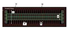
도 1a는 종래기술에 따른 반도체 장치의 퓨브부를 도시한 평면도이고, 도 1b는 도 1a에 도시된 Y-Y` 절취선을 따라 도시한 단면도이다.FIG. 1A is a plan view illustrating a fuse part of a semiconductor device according to the related art, and FIG. 1B is a cross-sectional view taken along the line Y-Y ′ of FIG. 1A.
도 1a 및 도 1b에 도시된 바와 같이, 소정의 하부 구조물이 구비된 기판(100) 상에 복수의 퓨즈(101)가 형성된다. 이때, 퓨즈(101)는 기형성된 캐패시터 상부전극, 금속배선 등을 이용하여 단층(single layer)으로 형성된다.As illustrated in FIGS. 1A and 1B, a plurality of
퓨즈(101) 상부에는 퓨즈(101)를 덮는 절연막(102)이 형성되어 있으며, 절연막(102)은 퓨즈박스(103)를 포함하고 있다. 이때, 퓨즈박스(103)의 퓨즈(101) 상부에는 소정 두께(T)의 절연막(102)이 잔류하고 있다.An
종래에는 상술한 바와 같은 퓨즈부를 형성한 후, 퓨즈박스(103)를 통하여 해당하는 퓨즈(101)에 레이저를 조사하여 퓨즈(101)를 컷팅(cutting)하는 퓨즈 블로잉(fuse blowing)방식을 사용하여 리페어를 수행하였다. 그러나, 퓨즈 블로잉 방식은 다음과 같은 문제점을 갖는다.Conventionally, after forming the fuse unit as described above, by using a fuse blowing method of cutting the
먼저, 퓨즈 컷팅을 용이하게 수행하기 위해서는 퓨즈(101) 상부에 잔류하는 절연막(102)의 두께(T)가 균일해야 한다. 하지만, 전 기판(100)에서 퓨즈(101) 상부에 잔류하는 절연막(102)의 두께(T)를 균일하게 형성하는 것이 매우 어려우며, 이로 인하여 퓨즈 컷팅이 정상적으로 이루어지지 않는 경우가 발생한다. 따라서, 리페어 수율(repair yield)이 감소하는 문제점이 있다.First, in order to easily perform the fuse cutting, the thickness T of the
또한, 퓨즈 컷팅시 발생하는 폭발력에 의하여 인접한 퓨즈(101)가 손상되는 문제점이 발생한다. 또한, 퓨즈 컷팅시 발생하는 폭발력에 의하여 도전성 부산 물(by product)이 생성되고, 생성된 도전성 부산물로 인하여 인접한 퓨즈(101)가 손상되거나, 인접한 퓨즈(101) 간 전기적단락이 발생하는 문제점이 있다.In addition, there is a problem that the
또한, 상술한 폭발력 및 도전성 부산물에 의한 문제점으로 인해 불가피하게 퓨즈(101)의 길이(L) 및 인접한 퓨즈(101) 간 간격(W)을 충분히 확보해야 한다. 이로 인하여 퓨즈부를 구비하는 반도체 장치의 집적도를 저하시키는 문제점이 있다.In addition, due to the problems caused by the explosive force and the conductive by-products described above, it is inevitably necessary to ensure a sufficient length (L) of the
본 발명은 상기한 종래기술의 문제점을 해결하기 위하여 제안된 것으로, 리페어 수율을 향상시킬 수 있는 반도체 장치의 퓨즈 및 그 제조방법을 제공하는데 그 목적이 있다.The present invention has been proposed to solve the above problems of the prior art, and an object thereof is to provide a fuse of a semiconductor device and a method of manufacturing the same which can improve a repair yield.
또한, 본 발명의 다른 목적은 퓨즈 블로잉 방식을 사용한 퓨즈 컷팅시 발생하는 퓨즈의 손상 및 전기적단락을 방지할 수 있는 반도체 장치의 퓨즈 및 그 제조방법을 제공하는데 있다.In addition, another object of the present invention is to provide a fuse of a semiconductor device and a method of manufacturing the same, which can prevent damage to the fuse and an electrical short generated when the fuse is cut using the fuse blowing method.
또한, 본 발명의 다른 목적은 퓨즈부의 집적도를 향상시킬 수 있는 반도체 장치의 퓨즈 및 그 제조방법을 제공하는데 있다.Another object of the present invention is to provide a fuse of a semiconductor device and a method of manufacturing the same, which can improve the degree of integration of the fuse unit.
상기 목적을 달성하기 위한 본 발명의 반도체 장치 퓨즈는, 제1도전패턴 및 상기 제1도전패턴의 상부에 상기 제1도전패턴과 소정 간격 이격되고, 상기 제1도전패턴의 끝단과 중첩(overlap)되는 중첩부를 구비하는 제2도전패턴을 포함한다. 이때, 상기 중첩부의 선폭은 상기 제1도전패턴의 선폭과 동일하거나, 또는 더 클 수 있다.The semiconductor device fuse of the present invention for achieving the above object is spaced apart from the first conductive pattern by a predetermined interval on the first conductive pattern and the first conductive pattern, and overlaps with an end of the first conductive pattern. And a second conductive pattern having an overlapping portion. In this case, the line width of the overlapping portion may be equal to or larger than the line width of the first conductive pattern.
상기 제1도전패턴은 하부 금속배선을 포함하고, 상기 제2도전패턴은 상부 금속배선을 포함할 수 있다.The first conductive pattern may include a lower metal wiring, and the second conductive pattern may include an upper metal wiring.
또한, 상기 중첩부는 아래로 연장된 지지막을 더 포함할 수 있다. 상기 지지 막은 상기 제1도전패턴의 측벽과 중첩되고, 좌우로 소정 간격 이격될 수 있으며, 금속물질막 또는 절연물질막을 포함할 수 있다. 상기 지지막은 상기 제2도전패턴과 동일물질일 수 있다. 상기 지지막은 질화막을 포함할 수 있다.In addition, the overlapping portion may further include a support membrane extended downward. The support layer overlaps the sidewall of the first conductive pattern, and may be spaced apart from the left and right by a predetermined distance, and may include a metal material layer or an insulating material layer. The support layer may be made of the same material as the second conductive pattern. The support layer may include a nitride film.
또한, 상기 중첩부의 양측벽 및 상기 지지막 측벽에 형성된 쇼트방지막을 더 포함할 수 있다. 상기 쇼트방지막은 절연물질막을 포함할 수 있다. 구체적으로, 상기 쇼트방지막은 산화막, 질화막 및 산화질화막으로 이루어진 그룹으로부터 선택된 어느 하나 또는 이들이 적층된 적층막을 포함할 수 있다.In addition, the anti-short film may be further formed on both sidewalls of the overlapping portion and the sidewall of the support layer. The anti-short film may include an insulating material film. Specifically, the anti-short film may include any one selected from the group consisting of an oxide film, a nitride film, and an oxynitride film or a laminated film in which they are stacked.
또한, 상기 제1도전패턴 및 상기 제2도전패턴을 포함하는 전체 구조물을 덮되, 적어도 상기 중첩부 및 상기 중첩부 아래 상기 제1도전패턴의 상부면을 노출시키는 오픈영역을 구비하는 절연막을 더 포함할 수 있다.The semiconductor device may further include an insulating layer covering the entire structure including the first conductive pattern and the second conductive pattern, and having an open area for exposing at least the overlapping portion and an upper surface of the first conductive pattern under the overlapping portion. can do.
상기 목적을 달성하기 위한 본 발명의 반도체 장치 퓨즈 제조방법은, 소정의 구조물이 구비된 기판상에 제1도전패턴을 형성하는 단계; 상기 제1도전패턴을 덮는 제1절연막을 형성하는 단계; 상기 제1절연막 상에 상기 제1도전패턴의 끝단과 중첩되는 중첩부를 구비하는 제2도전패턴을 형성하는 단계; 상기 제2도전패턴을 덮는 제2절연막을 형성하는 단계 및 상기 제2절연막 및 상기 제1절연막을 선택적으로 식각하여 적어도 상기 중첩부 및 상기 중첩부 아래 상기 제1도전패턴의 상부면을 노출시키는 오픈영역을 형성하는 단계를 포함한다. 이때, 상기 중첩부의 선폭은 상기 제1도전패턴의 선폭과 동일하거나, 또는 더 크게 형성할 수 있다.The semiconductor device fuse manufacturing method of the present invention for achieving the above object comprises the steps of: forming a first conductive pattern on a substrate having a predetermined structure; Forming a first insulating layer covering the first conductive pattern; Forming a second conductive pattern on the first insulating layer, the second conductive pattern including an overlapping portion overlapping with an end of the first conductive pattern; Forming a second insulating layer covering the second conductive pattern and selectively etching the second insulating layer and the first insulating layer to expose at least the overlapping portion and an upper surface of the first conductive pattern under the overlapping portion; Forming a region. In this case, the line width of the overlapping portion may be the same as or larger than the line width of the first conductive pattern.
상기 오픈영역을 형성하는 단계는, 상기 제2절연막을 선택적으로 식각하여 상기 중첩부의 상부면 및 측벽을 노출시키는 단계 및 상기 중첩부 아래 상기 제1도 전패턴의 상부면이 노출될때까지 상기 제1절연막을 선택적으로 식각하는 단계를 포함할 수 있다. 이때, 상기 제2절연막을 선택적으로 식각하는 단계는 건식식각법을 사용하여 실시할 수 있고, 상기 제1절연막을 선택적으로 식각하는 단계는 습식식각법을 사용하여 실시할 수 있다.The forming of the open region may include selectively etching the second insulating layer to expose the top surface and the sidewall of the overlapping portion and the first surface of the first conductive pattern under the overlapping portion until the top surface of the first conductive pattern is exposed. And selectively etching the insulating film. In this case, selectively etching the second insulating layer may be performed by using a dry etching method, and selectively etching the first insulating layer may be performed by using a wet etching method.
상기 제1도전패턴은 하부 금속배선을 포함하고, 상기 제2도전패턴은 상부 금속배선을 포함할 수 있다.The first conductive pattern may include a lower metal wiring, and the second conductive pattern may include an upper metal wiring.
또한, 상기 제2도전패턴을 형성하기 이전에, 상기 중첩부 아래로 연장된 지지막을 형성하는 단계를 더 포함할 수 있다. 상기 지지막을 형성하는 단계는, 상기 제1절연막을 선택적으로 식각하여 상기 제1도전패턴의 측벽과 중첩되고, 상기 제1도전패턴과 좌우로 소정 간격 이격된 리세스패턴을 형성하는 단계 및 상기 리세스패턴을 금속물질막 또는 절연물질막으로 매립하는 단계를 포함할 수 있다. 상기 지지막을 금속물질막으로 형성하는 경우, 상기 지지막을 형성함과 동시에 상기 제2도전패턴을 형성할 수 있다. 상기 절연물질막은 질화막을 포함할 수 있다.In addition, before forming the second conductive pattern, the method may further include forming a support layer extending below the overlapping portion. The forming of the support layer may include selectively etching the first insulating layer to form a recess pattern overlapping a sidewall of the first conductive pattern and spaced apart from the first conductive pattern by a predetermined distance. The method may include filling the set pattern with a metal material layer or an insulating material layer. When the support layer is formed of a metal material layer, the support layer may be formed and the second conductive pattern may be formed. The insulating material film may include a nitride film.
또한, 상기 오픈영역을 형성한 후, 상기 중첩부 양측벽 및 상기 지지막 측벽에 쇼트방지막을 형성하는 단계를 더 포함할 수 있다. 상기 쇼트방지막을 형성하는 단계는, 상기 오픈영역을 포함하는 구조물 전면에 쇼트방지막용 절연막을 형성하는 단계 및 전면식각공정을 실시하여 상기 쇼트방지막용 절연막을 상기 중첩부 양측벽 및 상기 지지막 측벽에 잔류시키는 단계를 포함할 수 있다. 상기 쇼트방지막은 산화막, 질화막 및 산화질화막으로 이루어진 그룹으로부터 선택된 어느 하나 또는 이들이 적층된 적층막으로 형성할 수 있다.The method may further include forming a short prevention film on both sidewalls of the overlapping portion and sidewalls of the support layer after forming the open region. The forming of the anti-short film may include forming an insulating film for an anti-short film on an entire surface of the structure including the open area and performing an entire surface etching process to deposit the insulating film for the anti-short film on both sidewalls of the overlapping portion and the sidewall of the supporting film. Residual may be included. The anti-short film may be formed of any one selected from the group consisting of an oxide film, a nitride film, and an oxynitride film or a laminated film in which they are stacked.
상술한 과제 해결 수단을 바탕으로 하는 본 발명은, 퓨즈 멜팅 방식을 사용하여 리페어 공정을 수행할 수 있는 다층 구조의 퓨즈를 구비함으로써, 퓨즈 블로잉 방식을 사용하여 리페어 공정 수행시 발생하는 문제점들을 원천적으로 방지할 수 있는 효과가 있다. 이를 통하여 본 발명은 반도체 장치의 신뢰성 및 수율을 향상시킬 수 있는 효과가 있다.The present invention based on the above-described problem solving means, by having a fuse of a multi-layer structure that can perform the repair process using the fuse melting method, the problems caused when performing the repair process using the fuse blowing method There is an effect that can be prevented. Through this, the present invention has the effect of improving the reliability and yield of the semiconductor device.
또한, 본 발명은 퓨즈부의 크기를 감소시킬 수 있으며, 이를 통하여 퓨즈부를 구비하는 반도체 장치의 집적도를 향상시킬 수 있는 효과가 있다.In addition, the present invention can reduce the size of the fuse, thereby improving the integration of the semiconductor device having a fuse.
이하 본 발명이 속하는 기술분야에서 통상의 지식을 가진자가 본 발명의 기술적 사상을 용이하게 실시할 수 있을 정도로 상세히 설명하기 위하여, 본 발명의 가장 바람직한 실시예를 첨부도면을 참조하여 설명하기로 한다.DETAILED DESCRIPTION OF THE PREFERRED EMBODIMENT Hereinafter, preferred embodiments of the present invention will be described in detail with reference to the accompanying drawings, in order to facilitate a person skilled in the art to easily carry out the technical idea of the present invention.
후술한 본 발명은 리페어 수율(repair yield)을 향상시킬 수 있는 반도체 장치의 퓨즈(fuse) 및 그 제조방법을 제공한다. 이를 위해 본 발명은 반도체 장치의 퓨즈를 소정영역이 중첩(overlap)된 중첩부를 갖는 다층(multy layer) 구조로 형성하는 것을 기술적 원리로 한다. 또한, 본 발명은 퓨즈 블로잉(fuse blowing) 방식이 아닌 퓨즈 멜팅(fuse melting) 방식을 사용하여 리페어(repair) 공정을 진행하는 것을 또 다른 기술적 원리로 한다.The present invention described below provides a fuse of a semiconductor device and a method of manufacturing the same, which can improve a repair yield. The technical principle of the present invention is to form a fuse of the semiconductor device in a multi-layer structure having an overlapping portion in which a predetermined region is overlapped. In addition, according to the present invention, it is another technical principle that a repair process is performed using a fuse melting method instead of a fuse blowing method.
상술한 본 발명의 기술적 원리는 퓨즈를 구비하는 모든 반도체 장치에 적용 이 가능하다. 이하, 본 발명의 기술적 원리가 적용된 퓨즈에 대하여 도 2a 내지 도 2c를 참조하여 자세히 설명한다.The technical principle of the present invention described above is applicable to all semiconductor devices having a fuse. Hereinafter, a fuse to which the technical principle of the present invention is applied will be described in detail with reference to FIGS. 2A to 2C.
도 2a 내지 도 2c는 본 발명의 제1실시예에 따른 반도체 장치의 퓨즈를 도시한 도면이다. 도 2a는 평면도, 도 2b는 도 2a에 도시된 X-X`절취선을 따라 도시한 단면도, 도 2c는 도 2a에 도시된 Y-Y`절취선을 따라 도시한 단면도이다.2A to 2C are diagrams illustrating a fuse of the semiconductor device according to the first embodiment of the present invention. FIG. 2A is a plan view, FIG. 2B is a cross-sectional view taken along the line X-X 'of FIG. 2A, and FIG. 2C is a cross-sectional view taken along the line Y-Y' of FIG. 2A.
도 2a 내지 도 2c에 도시된 바와 같이, 본 발명의 퓨즈는 소정의 구조물이 구비된 기판(200) 상의 제1도전패턴(201), 제1도전패턴(201) 상부에 제1도전패턴(201)과 소정간격 이격되고, 제1도전패턴(201)의 끝단과 중첩(overlap)되는 중첩부(202A)를 구비하는 제2도전패턴(202)을 포함한다. 또한, 중첩부(202A) 아래로 연장된 지지막(203) 및 중첩부(202)의 양측벽 및 지지막(203)의 측벽에 형성된 쇼트방지막(204)을 더 포함할 수 있다. 또한, 제1도전패턴(201) 및 제2도전패턴(202)을 포함하는 구조물 전면을 덮고, 적어도 중첩부(202A) 및 중첩부(202A) 아래 제1도전패턴(201)의 상부면을 노출시키는 오픈영역(205)을 구비하는 절연막(206)을 더 포함할 수 있다. 이때, 오픈영역(205)은 통상적으로 퓨즈박스라 불리우며, 중첩부(202A)와 제1도전패턴(201) 사이에는 공극(air gap)이 형성된다.As shown in FIGS. 2A to 2C, the fuse of the present invention may include a first
제1도전패턴(201) 및 제2도전패턴(202)은 퓨즈로 작용하며, 기판(200)에 기형성된 도전막 예컨대, 캐패시터 상부전극 또는 금속배선을 사용하여 형성할 수 있다. 예를 들어, TLM(Triple Layers of Metal) 구조의 금속배선 즉, 제1, 제2 및 제3금속배선을 구비하는 반도체 장치의 경우, 제2도전패턴(202)은 최상층 금속배선인 제3금속배선을 사용하여 형성할 수 있으며, 제1도전패턴(201)은 최상층 금속배선 아래 금속배선인 제2금속배선을 사용하여 형성할 수 있다. 즉, 제1도전패턴(201)으로 하부 금속배선을 사용할 수 있고, 제2도전패턴(202)으로 상부 금속배선을 사용할 수 있다. 이처럼, 본 발명의 퓨즈는 제1도전패턴(201)과 제2도전패턴(202)으로 이루어진 다층(multi layer) 구조를 갖는 것을 특징으로 한다.The first
제1도전패턴(201) 및 제2도전패턴(202)은 금속물질막을 포함할 수 있다. 즉, 제1도전패턴(201) 및 제2도전패턴(202)은 금속막, 도전성 금속질화막, 도전성 금속산화막 및 금속실리사이드막으로 이루어진 그룹으로부터 선택된 어느 하나 또는 이들이 적층된 적층막으로 형성할 수 있다. 금속막은 텅스텐(W), 알루미늄(Al), 티타늄(Ti)등을 사용할 수 있다. 도전성 금속질화막으로는 티타늄질화막(TiN), 도전성 금속산화막으로는 이리듐산화막(IrO2), 금속실리사이드막으로는 텅스텐실리사이드(WSi), 티타늄실리사이드(TiSi) 등을 사용할 수 있다.The first
중첩부(202A)는 제2도전패턴(202)와 동일 물질로 형성할 수 있다. 즉, 중첩부(202A)는 금속물질막을 포함할 수 있다.The overlapping
중첩부(202A)의 선폭(W2)은 제1도전패턴(201)의 선폭(W1)과 동일하게 형성하거나(W2 = W1), 또는 더 크게 형성할 수 있다(W2 > W1). 이때, 중첩부(202A)는 리페어 공정시 레이저(laser)가 조사되는 영역으로 레이저 직경, 제1도전패턴(201)과의 중첩면적을 고려하여 중첩부(202A)의 선폭(W2)은 제1도전패턴(201)의 선폭(W1)보다 크게 형성하는 것이 바람직하다. 또한, 중첩부(202A)의 선폭(W2)은 제2도전패턴(202)의 선폭(W3)과 동일하거나, 또는 더 클 수 있다.The line width W2 of the overlapping
지지막(203)은 중첩부(202A)와 중첩부(202A) 아래 제1도전패턴(201) 사이에 소정 간격을 유지할 수 있도록 중첩부(202A)를 지지하는 역할을 수행한다. 또한, 이와 동시에 지지막(203)은 리페어 공정시 레이저에 의하여 멜팅(melting)된 중첩부(202A)에 의하여 인접한 퓨즈가 손상되거나, 또는 인접한 퓨즈 사이에 전기적단락이 발생하는 것을 방지하는 역할을 수행한다. 이때, 지지막(203)이 상술한 역할을 효과적으로 수행하기 위하여 지지막(203)의 일부가 절연막(206)에 박힌 구조를 갖도록 형성하는 것이 바람직하다. 예를 들어, 지지막(203)의 하부면을 기준으로 500Å ~ 1000Å 범위의 두께가 절연막(206)에 박힌(또는 매립된) 구조를 갖도록 형성하는 것이 바람직하다.The
상술한 역할을 수행하는 지지막(203)은 금속물질막 또는 절연물질막으로 형성할 수 있다. 지지막(203)을 금속물질막으로 형성할 경우, 지지막은(203)은 제2도전패턴(202)과 동일 물질로 형성하는 것이 바람직하다. 이는 지지막(203)과 제2도전패턴(202)을 동일 물질로 형성할 경우, 공정과정을 단순화시킬 수 있기 때문이다. 이때, 리페어 공정을 수행하기 이전에 지지막(203)으로 인해 제1도전패턴(201)과 제2도전패턴(202) 사이에 전기적단락이 발생하는 것을 방지하기 위하여 지지막(203)은 제1도전패턴(201)의 측벽과 중첩되고, 제1도전패턴(201)으로부터 좌우로 소정 간격 이격되도록 형성하는 것이 바람직하다.The
지지막(203)을 절연물질막으로 형성할 경우, 절연막(206)과 식각선택비를 갖는 절연물질로 형성하는 것이 바람직하다. 예를 들어, 절연막(206)을 산화막으로 형성할 경우, 지지막(203)은 질화막으로 형성하는 것이 바람직하다. 질화막으로는 실리콘질화막(Si3N4)을 사용할 수 있다. 지지막(203)을 절연물질막으로 형성할 경우, 지지막(203)의 측벽과 제1도전패턴(201)의 측벽이 서로 접하도록 형성할 수도 있다. 바람직하게는, 리페어 공정시 멜팅된 중첩부(202A)와 제1도전패턴(201) 사이의 접촉면적을 확보하기 위하여 제1도전패턴(201)의 측벽과 중첩되고, 제1도전패턴(201)으로부터 좌우로 소정 간격 이격되도록 지지막(203)을 형성하는 것이 좋다.When the supporting
쇼트방지막(204)은 지지막(203)과 더불어서 리페어 공정시 레이저에 의하여 멜팅된 중첩부(202A)에 의하여 인접한 퓨즈가 손상되거나, 또는 인접한 퓨즈 사이가 전기적으로 단락되는 것을 방지하는 역할을 수행한다. 쇼트방지막(204)은 절연물질막으로 형성할 수 있다. 예컨대, 쇼트방지막(206)은 산화막, 질화막 및 산화질화막으로 이루어진 그룹으로부터 선택된 어느 하나 또는 이들이 적층된 적층막으로 형성할 수 있다.The
제1도전패턴(201) 및 제2도전패턴(202)을 포함하는 전체 구조물을 덮는 절연막(206)은 제1도전패턴(201) 및 제2도전패턴(202)을 포함하는 전체 구조물을 보호하는 역할을 수행한다. 또한, 절연막(206)은 오픈영역(205)으로 인해 노출된 중첩부(202A)를 구비하는 제2도전패턴(202)이 제1도전패턴(201)과 상하로 소정 간격을 유지할 수 있도록 제2도전패턴(202)을 지지하는 역할을 수행한다.The insulating
절연막(206)은 산화막, 질화막, 산화질화막 및 탄소함유막으로 이루어진 그룹으로부터 선택된 어느 하나 또는 이들이 적층된 적층막으로 형성할 수 있다. 구체적으로, 절연막(206)은 제1도전패턴(201)을 덮는 제1절연막(206A) 및 제2도전패 턴(202)을 덮는 제2절연막(206B)을 포함할 수 있다. 이때, 제1절연막(206A)은 산화막일 수 있으며, 제2절연막(206B)은 산화막, 질화막, 산화질화막 및 탄소함유막으로 이루어진 그룹으로부터 선택된 어느 하나 또는 이들이 적층된 적층막일 수 있다. 산화막으로는, 실리콘산화막(SiO2), BPSG(Boron Phosphorus Silicate Glass), PSG(Phosphorus Silicate Glass), TEOS(Tetra Ethyle Ortho Silicate), USG(Un-doped Silicate Glass), SOG(Spin On Glass), 고밀도플라즈마산화막(High Density Plasma, HDP), SOD(Spin On Dielectric) 등을 사용할 수 있다. 질화막으로는 실리콘질화막(Si3N4)을 사용할 수 있고, 산화질화막으로는 실리콘산화질화막(SiON)을 사용할 수 있다. 그리고, 탄소함유막으로는 비정질탄소막(amorphous carbon layer), 폴리이미드(polyimide), SiOC, SOC 등을 사용할 수 있다.The insulating
상술한 구조를 갖는 본 발명의 퓨즈는 퓨즈 블로잉 방식 대신에 퓨즈 멜팅 방식을 사용하여 리페어공정을 진행함으로써, 퓨즈 블로잉 방식을 사용하여 리페어 공정을 진행하는 과정에서 발생하는 문제점들을 원천적으로 방지할 수 있는바, 이를 도 3a를 참조하여 자세히 설명한다.The fuse of the present invention having the above-described structure by using the fuse melting method instead of the fuse blowing method of the repair process, it is possible to prevent the problems caused in the process of the repair process using the fuse blowing method at the source This will be described in detail with reference to FIG. 3A.
도 3a는 종래기술에 따른 퓨즈 블로잉 방식의 리페어 공정과 본 발명의 퓨즈 멜팅 방식의 리페어 공정을 비교하여 도시한 단면도이다. 여기서, 설명의 편의를 위하여 종래기술에 따른 퓨즈는 도 1b에 도시된 도면 및 도면부호를 사용하고, 본 발명의 퓨즈는 도 2c에 도시된 도면 및 도면부호를 사용하였다.3A is a cross-sectional view illustrating a repair process of a fuse blowing method according to the related art and a repair process of a fuse melting method according to the present invention. Here, for convenience of description, the fuse according to the prior art uses the drawings and the reference numerals shown in Figure 1b, the fuse of the present invention used the drawings and reference numerals shown in Figure 2c.
도 3a에 도시된 바와 같이, 퓨즈 블로잉 방식은 전기적으로 연결되어 있는 퓨즈(101)를 레이저를 사용하여 컷팅(cutting)하는 방법으로 리페어 공정을 진행한다. 앞서 언급한 바와 같이, 상술한 퓨즈 블로잉 방식은 퓨즈 컷팅을 용이하게 수행하기 위하여 퓨즈(101) 상에 잔류하는 절연막(102)의 두께를 전 기판(100)에서 균일하게 제어하기 어렵고, 이로 인해 리페어 수율이 저하되는 문제점이 있다. 또한, 퓨즈 컷팅시 발생하는 폭발력 및 도전성 부산물로 의하여 인접한 퓨즈(101)가 손상되거나, 또는 인접한 퓨즈간 전기적단락이 발생하는 문제점이 있다.As shown in FIG. 3A, the fuse blowing method performs a repair process by cutting a
이에 반하여, 본 발명의 퓨즈 멜팅 방식은 안티퓨즈(anti-fuse)와 그 구동원리가 유사하다. 구체적으로, 퓨즈 멜팅 방식은 전기적으로 분리된 제1도전패턴(201)과 제2도전패턴(202)으로 이루어진 퓨즈를 구비하고, 제2도전패턴(202)의 중첩부(202A)에 레이저를 조사하여 중첩부(202A)를 멜팅(melting)시킴으로써, 제1도전패턴(201)과 제2도전패턴(202)을 전기적으로 연결시키는 방법으로 리페어 공정을 진행한다.On the contrary, the fuse melting method of the present invention is similar to anti-fuse and its driving principle. In detail, the fuse melting method includes a fuse including an electrically separated first
이와 같이, 본 발명의 퓨즈는 퓨즈 멜팅 방식을 사용함으로써, 퓨즈 (즉, 제1도전패턴(201) 및 제2도전패턴(202)) 상에 절연막(206)을 잔류시킬 필요가 없다. 따라서, 퓨즈 상부에 잔류하는 절연막(206) 두께의 균일도 저하에 따른 리페어 수율 저하를 원천적으로 방지할 수 있다.As such, the fuse of the present invention does not need to leave the insulating
또한, 본 발명은 리페어 공정시 폭발력을 이용하지 않기 때문에 폭발력에 의하여 인접한 퓨즈의 손상을 방지할 수 있다. 또한, 폭발력에 기인한 도전성 부산물의 생성을 방지할 수 있으며, 이를 통하여 도전성 부산물에 기인한 퓨즈 손상 및 전기적 단락을 방지할 수 있다.In addition, since the present invention does not use the explosive force during the repair process, damage to adjacent fuses can be prevented by the explosive force. In addition, it is possible to prevent the generation of conductive by-products due to the explosive force, thereby preventing the fuse damage and electrical short circuit caused by the conductive by-products.
또한, 본 발명은 퓨즈 블로잉 방식보다 적은 레이저 에너지를 사용하여 리페어 공정을 진행할 수 있기 때문에 리페어 공정에 대한 안정성을 향상시킬 수 있다. 예를 들어, 아르곤 레이저를 사용하고 퓨즈를 알루미늄으로 형성한 경우, 퓨즈 블로잉 방식은 0.21uj ~ 0.25uj 범위의 에너지를 필요로 하지만, 본 발명의 퓨즈 멜팅 방식은 0.18uj ~ 0.20uj 범위를 에너지를 사용하여 리페어 공정을 진행할 수 있다.In addition, the present invention can improve the stability of the repair process because the repair process can be performed using less laser energy than the fuse blowing method. For example, if an argon laser is used and the fuse is formed of aluminum, the fuse blowing method requires energy in the range of 0.21uj to 0.25uj, but the fuse melting method of the present invention uses energy in the range of 0.18uj to 0.20uj. Can be used to proceed with the repair process.
결과적으로 본 발명은 반도체 장치의 신뢰성 및 수율을 향상시킬 수 있다.As a result, the present invention can improve the reliability and yield of the semiconductor device.
또한, 본 발명의 퓨즈는 퓨즈 멜팅 방식을 사용함으로써, 퓨즈부의 크기를 감소시킬 수 있는 바, 이를 도 3b 및 도 3c를 참조하여 자세히 설명한다.In addition, the fuse of the present invention can reduce the size of the fuse part by using a fuse melting method, which will be described in detail with reference to FIGS. 3B and 3C.
도 3b는 종래기술에 따른 퓨즈 블로잉 방식의 퓨즈부를 나타낸 평면이미지이고, 도 3c는 본 발명의 퓨즈 멜팅 방식의 퓨즈부를 비교하여 도시한 평면도이다. 여기서는 설명의 편의를 위하여 50nm급 디자인 룰이 적용된 반도체 장치의 퓨즈부를 예시하여 설명한다.Figure 3b is a planar image showing a fuse blowing method of the fuse according to the prior art, Figure 3c is a plan view comparing the fuse of the fuse melt method of the present invention. For convenience of explanation, the fuse unit of the semiconductor device to which the 50 nm design rule is applied will be described.
도 3b 및 도 3c에 도시된 바와 같이, 종래기술에 따른 퓨즈부는 퓨즈 컷팅시 발생하는 폭발력 및 도전성 부산물에 의한 인접 퓨즈의 손상 및 전기적단락을 방지하기 위하여 불가피하게 퓨즈(101)의 길이(L1) 및 인접한 퓨즈간 간격(W4)을 충분히 확보해야만 한다. 예컨대, 50nm급 디자인 룰에서 퓨즈(101)의 길이(L1)는 9um 이상, 퓨즈(101) 간 간격(W4)은 2um 이상, 퓨즈박스(Fuse Open Size, 103)의 선폭(L2)은 4um 이상을 확보해야만 한다. 그리고, 퓨즈(101)의 선폭(W5)은 0.5um이 다.As shown in FIGS. 3B and 3C, the fuse part according to the related art inevitably has a length L1 of the
이에 반하여, 본 발명의 퓨즈는 퓨즈 멜팅 방식을 사용하기 때문에 폭발력 및 도전성 부산물에 기인한 문제점을 원천적으로 방지할 수 있다. 따라서, 퓨즈(즉, 제1도전패턴(201) 및 제2도전패턴(202))의 길이(L3)는 9um 이하, 퓨즈 간 간격(W6)은 2um 이하, 오픈영역(205)의 선폭(L4)은 4um 이하로 형성할 수 있다.On the contrary, since the fuse of the present invention uses a fuse melting method, problems due to explosive force and conductive by-products can be prevented. Accordingly, the length L3 of the fuses (that is, the first
퓨즈를 구성하는 제1도전패턴(201)의 선폭(W1)과 제2도전패턴(202)의 선폭(W3)의 선폭은 동일할 수 있으며, 중첩부(202A)의 선폭(W2)은 제1도전패턴(201)의 선폭(W1)과 동일하거나 더 클 수 있다. 예컨대, 50nm급 디자인 룰에서 중첩부(202)의 선폭(W2)은 0.5um ~ 1um 범위를 갖고, 중첩부(202)의 길이(L5)는 1um ~ 2um 범위를 갖도록 형성하는 것이 바람직하다.The line width W1 of the first
이와 같이, 본 발명의 퓨즈는 퓨즈 멜팅 방식을 사용함으로써, 퓨즈부의 크기를 감소시킬 수 있으며, 이를 통하여 퓨즈부를 구비하는 반도체 장치의 집적도를 향상시킬 수 있다.As described above, the fuse of the present invention can reduce the size of the fuse part by using a fuse melting method, thereby improving the degree of integration of the semiconductor device including the fuse part.
이하, 본 발명에 따른 반도체 장치의 퓨즈 제조방법에 대한 실시예를 첨부한 도면을 참조하여 설명한다. 이하의 실시예에서는 50nm급 디자인 룰이 적용된 반도체 장치의 퓨즈를 예시하여 설명한다. 따라서, 이하의 실시예에서 언급된 수치는 실시예를 위한 수치이며, 절대적인 의미를 갖지 않는다.Hereinafter, an embodiment of a fuse manufacturing method of a semiconductor device according to the present invention will be described with reference to the accompanying drawings. In the following embodiment, a fuse of a semiconductor device to which a 50 nm-class design rule is applied will be described. Accordingly, the numerical values mentioned in the following examples are numerical values for the examples, and have no absolute meaning.
도 4a 내지 도 4e, 도 5a 내지 도 5e 및 도 6a 내지 도 6e는 본 발명의 제2실시예에 따른 반도체 장치의 퓨즈 제조방법을 도시한 도면이다. 여기서, 도 4a 내지 도 4e는 평면도, 도 5a 내지 도 5e는 도 4a 내지 도 4e에 도시된 X-X` 절취선을 따라 도시한 단면도, 도 6a 내지 도 6e는 도 4a 내지 도 4e에 도시된 Y-Y`절취선을 따라 도시한 단면도이다.4A through 4E, 5A through 5E, and 6A through 6E illustrate a method of manufacturing a fuse of a semiconductor device in accordance with a second embodiment of the present invention. 4A to 4E are plan views, FIGS. 5A to 5E are cross-sectional views taken along the line XX ′ of FIG. 4A to 4E, and FIGS. 6A to 6E are YY ′ cut lines shown to FIGS. 4A to 4E. It is a cross-sectional view shown along.
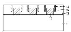
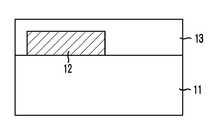
도 4a, 도 5a 및 도 6a에 도시된 바와 같이, 소정의 구조물이 구비된 기판(11) 상에 복수의 제1도전패턴(12)을 형성한다. 제1도전패턴(12)은 금속물질막으로 형성할 수 있다. 즉, 제1도전패턴(12)은 금속막, 도전성 금속질화막, 도전성 금속산화막 및 금속실리사이드막으로 이루어진 그룹으로부터 선택된 어느 하나 또는 이들이 적층된 적층막으로 형성할 수 있다. 금속막은 텅스텐(W), 알루미늄(Al), 티타늄(Ti)등을 사용할 수 있다. 도전성 금속질화막으로는 티타늄질화막(TiN), 도전성 금속산화막으로는 이리듐산화막(IrO2), 금속실리사이드막으로는 텅스텐실리사이드(WSi), 티타늄실리사이드(TiSi) 등을 사용할 수 있다.As shown in FIGS. 4A, 5A, and 6A, a plurality of first
또한, 제1도전패턴(12)은 별도의 금속물질막 증착 및 패터닝공정을 통하여 형성하지 아니하고, 패캐시터의 상부전극 또는 금속배선을 사용하여 형성할 수 있다. 이때, 금속배선을 사용하여 제1도전패턴(12)을 형성할 경우, 최상층 금속배선 아래의 금속배선을 사용하여 형성할 수 있다.In addition, the first
다음으로, 제1도전패턴(12)을 덮는 제1절연막(13)을 형성한다. 제1절연막(13)은 산화막으로 형성할 수 있다. 산화막으로는 실리콘산화막(SiO2), BPSG(Boron Phosphorus Silicate Glass), PSG(Phosphorus Silicate Glass), TEOS(Tetra Ethyle Ortho Silicate), USG(Un-doped Silicate Glass), SOG(Spin On Glass), 고밀도플라즈마산화막(High Density Plasma, HDP), SOD(Spin On Dielectric) 등을 사용할 수 있다.Next, a first insulating
다음으로, 제1절연막(13) 상에 지지막을 형성하기 위한 포토레지스트패턴(미도시)을 형성한 후, 포토레지스패턴을 식각장벽(etch barrier)으로 제1절연막(13)을 리세스(recess) 식각하여 리세스패턴(14)을 형성한다. 이때, 리세스패턴(14)의 측벽이 제1도전패턴(12)의 측벽 일부 또는 전부와 중첩(overlap)되도록 형성할 수 있다. 또한, 리세스패턴(14)은 제1도전패턴(12)의 측벽으로부터 좌우로 소정 간격 이격되도록 형성하는 것이 바람직하다.Next, after forming a photoresist pattern (not shown) for forming a support layer on the first insulating
다음으로, 리세스패턴(14)을 금속물질막 또는 절연물질막으로 매립하여 지지막(15)을 형성한다. 지지막(15)은 후속 공정을 통하여 형성될 중첩부를 구비하는 제2도전패턴과 제1도전패턴(12)이 상하로 소정 간격을 유지할 수 있도록 중첩부를 지지하는 역할을 수행함과 동시에 후속 리페어 공정시 레이저에 의하여 멜팅(melting)된 중첩부에 의하여 인접한 퓨즈가 손상되거나, 또는 인접한 퓨즈 사이에 전기적단락이 발생하는 것을 방지하는 역할을 수행한다.Next, the
지지막(15)을 금속물질막을 사용하여 형성할 경우, 리페어 공정을 수행하기 이전에 지지막(15)으로 인해 제1도전패턴(12)과 제2도전패턴 사이에 전기적단락이 발생하는 것을 방지하기 위하여 지지막(15)은 제1도전패턴(12)과 소정 간격 이격되도록 형성하는 것이 바람직하다. 따라서, 지지막(15)을 금속물질막으로 형성하고자 할 경우, 리세스패턴(14)의 측벽은 제1도전패턴(12)의 측벽과 중첩되고, 제1도전패턴(12)의 측벽으로부터 좌우로 소정 간격 이격되도록 형성하는 것이 바람직하다.When the
지지막(15)을 절연물질막으로 형성할 경우, 지지막(15)은 제1절연막(13)과 식각선택비를 갖는 절연물질로 형성하는 것이 바람직하다. 예를 들어, 제1절연 막(13)을 산화막으로 형성할 경우, 지지막(15)은 질화막으로 형성하는 것이 바람직하다. 질화막으로는 실리콘질화막(Si3N4)을 사용할 수 있다. 지지막(15)을 절연물질막으로 형성할 경우, 지지막(15)과 제1도전패턴(12)이 서로 접하도록 형성하여도 전기적으로 무방하다. 따라서, 지지막(15)을 절연물질막으로 형성할 경우, 리세스패턴(14)은 제1도전패턴(12)의 측벽을 노출시키도록 형성할 수도 있다. 이 경우, 인접한 퓨즈간 간격을 더욱더 감소시킬 수 있다.When the supporting
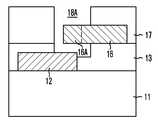
도 4b, 도 5b 및 도 6b에 도시된 바와 같이, 제1절연막(13) 상에 제1도전패턴(12) 끝단과 중접되는 중첩부(16A)를 구비하는 제2도전패턴(16)을 형성한다. 이때, 제2도전패턴(16)의 중첩부(16A)는 지지막(15)을 덮도록 형성하는 것이 바람직하다. 제2도전패턴(16)은 금속배선을 사용하여 형성할 수 있으며, 다층의 금속배선을 갖는 반도체 장치에서 최상층 금속배선을 사용하여 형성할 수 있다.As shown in FIGS. 4B, 5B, and 6B, the second
제2도전패턴(16)은 금속물질막으로 형성할 수 있다. 이때, 지지막(15)을 금속물질막으로 형성할 경우, 지지막(15) 형성공정과 제2도전패턴(16) 형성공정을 동시에 진행할 수 있다. 예를 들어, 제2도전패턴(16)을 형성하기 위하여 제1절연막(13) 전면에 도전막을 형성할 때, 도전막이 리세스패턴(14)을 매립함과 동시에 제1절연막(13) 전면을 덮도록 형성하면 지지막(15)과 제2도전패턴(16)을 동시에 형성할 수 있다. 즉, 지지막(15)을 금속물질막으로 형성할 경우, 공정과정을 단순화시킬 수 있다.The second
제1도전패턴(12)의 끝단과 중접되는 중첩부(16A)의 선폭(W2)은 제1도전패 턴(12)의 선폭(W1)과 동일하게 형성하거나, 또는 더 크게 형성할 수 있다. 이때, 중첩부(16A)는 리페어 공정시 레이저(laser)가 조사되는 영역으로 레이저 직경, 제1도전패턴(12)과의 중첩면적을 고려하여 중첩부(16A)의 선폭(W2)은 제1도전패턴(12)의 선폭(W1)보다 크게 형성하는 것이 바람직하다. 예를 들어, 중첩부(16A)의 선폭(W2)은 0.5um ~ 1um 범위를 갖고, 중첩부(16A)의 길이(L5)는 1um ~ 2um 범위를 갖도록 형성할 수 있다. 또한, 중첩부(16A)의 선폭(W2)은 제2도전패턴(16)의 선폭(W3)과 동일하거나, 또는 더 클 수 있다.The line width W2 of the overlapping
도 4c, 도 5c 및 도 6c에 도시된 바와 같이, 제2도전패턴(16)을 포함하는 구조물 전면에 제2절연막(17)을 형성한다. 제2절연막(17)은 제2도전패턴(16)을 포함하는 전체 구조물을 보호하는 역할을 수행한다. 또한, 제2절연막(17)은 지지막(15)과 더불어 후속 공정을 통하여 노출될 중첩부(16A)를 구비하는 제2도전패턴(16)이 제1도전패턴(12)과 소정간격을 유지할 수 있도록 제2도전패턴(16)을 지지하는 역할을 수행한다.As shown in FIGS. 4C, 5C, and 6C, the second insulating
제2절연막(17)은 산화막, 질화막, 산화질화막 및 탄소함유막으로 이루어진 그룹으로부터 선택된 어느 하나 또는 이들이 적층된 적층막으로 형성할 수 있다. 산화막으로는, 실리콘산화막(SiO2), BPSG(Boron Phosphorus Silicate Glass), PSG(Phosphorus Silicate Glass), TEOS(Tetra Ethyle Ortho Silicate), USG(Un-doped Silicate Glass), SOG(Spin On Glass), 고밀도플라즈마산화막(High Density Plasma, HDP), SOD(Spin On Dielectric) 등을 사용할 수 있다. 질화막으로는 실리 콘질화막(Si3N4)을 사용할 수 있고, 산화질화막으로는 실리콘산화질화막(SiON)을 사용할 수 있다. 그리고, 탄소함유막으로는 비정질탄소막(amorphous carbon layer), 폴리이미드(polyimide), SiOC, SOC 등을 사용할 수 있다.The second insulating
다음으로, 제2절연막(17) 상에 포토레지스트패턴(미도시)을 형성한 후, 포토레지스트패턴을 식각장벽으로 제2절연막(17)을 식각하여 적어도 중첩부(16A)를 노출시키는 오픈영역(18)을 형성한다. 구체적으로, 포토레지스트패턴을 식각장벽으로 제2절연막(17)을 식각하여 중첩부(16A)의 상부면 및 측벽이 노출되도록 오픈영역(18)을 형성하는 것이 바람직하다. 이때, 오픈영역(18)은 통상적으로 퓨즈박스라 불리운다.Next, after forming a photoresist pattern (not shown) on the second insulating
오픈영역(18)을 형성하기 위한 식각공정은 건식식각법(dry etch)을 사용하여 실시하는 것이 바람직하다.The etching process for forming the
도 4d, 도 5d 및 도 6d에 도시된 바와 같이, 오픈영역(18)으로 인해 노출된 제1절연막(13)을 일부 식각하여 중첩부(16A) 아래의 제1도전패턴(12)의 상부면을 노출시킨다. 이하, 제1절연막(13)이 일부 식각되면서 확장된 오픈영역(18)의 도면부호를 '18A'로 변경하여 표기한다.As shown in FIGS. 4D, 5D, and 6D, the first insulating
제1도전패턴(12)의 상부면을 노출시키기 위한 식각공정은 습식식각법(wet etch)을 사용하여 실시하는 것이 바람직하다. 예컨대, 제1절연막(13)을 산화막으로 형성한 경우, BOE(Buffered Oxide Echant) 또는 불산(HF)용액을 사용하여 식각공정을 진행할 수 있다.The etching process for exposing the upper surface of the first
상술한 공정과정을 통하여 제1도전패턴(12)과 중첩부(16A) 사이에 공극(air gap)이 형성되고, 상하로 소정 간격 이격된 다층 구조의 퓨즈를 형성할 수 있다.Through the above-described process, an air gap may be formed between the first
도 4e, 도 5e 및 도 6e에 도시된 바와 같이, 오픈영역(18A)을 포함하는 구조물 전면에 쇼트방지막용 절연막을 형성한 후, 전면식각공정을 실시하여 중첩부(16A)의 양측벽 및 지지막(15)의 측벽에 쇼트방지막용 절연막을 잔류시켜 쇼트방지막(19)을 형성한다. 쇼트방지막(19)은 지지막(15)과 더불어서 리페어 공정시 멜팅된 중첩부(16)가 인접한 퓨즈와 전기적으로 단락되는 것을 방지하는 역할을 수행하는 것으로, 절연물질막으로 형성할 수 있다. 쇼트방지막(19)은 산화막, 질화막 및 산화질화막으로 이루어진 그룹으로부터 선택된 어느 하나 또는 이들이 적층된 적층막으로 형성할 수 있다.As shown in FIGS. 4E, 5E, and 6E, after forming an insulating film for anti-short film on the front surface of the structure including the
상술한 공정과정을 통하여 본 발명의 반도체 장치 퓨즈를 완성할 수 있다.Through the above-described process, the semiconductor device fuse of the present invention can be completed.
이와 같이, 본 발명의 퓨즈는 퓨즈 멜팅 방식을 사용하여 리페어 공정을 진행할 수 있는 다층 구조의 퓨즈를 형성함으로써, 퓨즈 블로잉 방식을 사용하여 리페어 공정을 진행하는 과정에서 발생하는 문제점들을 원천적으로 방지할 수 있다. 이를 통하여 본 발명은 퓨즈부의 크기를 감소시킬 수 있으며, 퓨즈부를 구비하는 반도체 장치의 집적도를 향상시킬 수 있다.As described above, the fuse of the present invention forms a multi-layered fuse capable of performing a repair process using a fuse melting method, thereby preventing problems occurring during the repair process by using a fuse blowing method. have. Accordingly, the present invention can reduce the size of the fuse unit and improve the integration degree of the semiconductor device including the fuse unit.
본 발명의 기술 사상은 상기 바람직한 실시예에 따라 구체적으로 기술되었으나, 상기 실시예는 그 설명을 위한 것이며, 그 제한을 위한 것이 아님을 주의하여야 한다. 또한, 본 발명의 기술분야의 통상의 전문가라면 본 발명의 기술사상의 범 위내의 다양한 실시예가 가능함을 이해할 수 있을 것이다.Although the technical spirit of the present invention has been described in detail according to the above preferred embodiment, it should be noted that the above embodiment is for the purpose of description and not of limitation. In addition, those skilled in the art will understand that various embodiments within the scope of the technical idea of the present invention are possible.
도 1a는 종래기술에 따른 반도체 장치의 퓨브부를 도시한 평면도.1A is a plan view illustrating a fuse part of a semiconductor device according to the related art.
도 1b는 도 1a에 도시된 Y-Y` 절취선을 따라 도시한 단면도.FIG. 1B is a cross-sectional view taken along the line Y-Y` shown in FIG. 1A; FIG.
도 2a 내지 도 2c는 본 발명의 제1실시예에 따른 반도체 장치의 퓨즈를 도시한 도면.2A to 2C illustrate a fuse of a semiconductor device according to a first embodiment of the present invention.
도 3a는 종래기술에 따른 퓨즈 블로잉 방식의 리페어 공정과 본 발명의 퓨즈 멜팅 방식의 리페어 공정을 비교하여 도시한 단면도.Figure 3a is a cross-sectional view showing a repair process of the fuse blowing method of the fuse blow method according to the prior art compared with the repair process of the present invention.
도 3b 및 도 3c는 종래기술에 따른 퓨즈 블로잉 방식의 퓨즈부와 본 발명의 퓨즈 멜팅 방식의 퓨즈부를 비교하여 도시한 평면도.Figure 3b and Figure 3c is a plan view showing a comparison between the fuse of the fuse blowing method according to the prior art fuse unit of the fuse melt method of the present invention.
도 4 내지 도 6은 본 발명의 제2실시예에 따른 반도체 장치의 퓨즈 제조방법을 도시한 도면.4 to 6 illustrate a method of manufacturing a fuse of a semiconductor device according to a second exemplary embodiment of the present invention.
*도면 주요 부분에 대한 부호 설명** Description of symbols on the main parts of the drawings *
201, 12 : 제1도전패턴202, 16 : 제1도전패턴201, 12: first
202A, 16A : 중첩부203, 15 : 지지막202A, 16A: overlapping
204, 19 : 쇼트방지막205, 18, 18A : 오픈영역204, 19:
206 : 절연막206: insulating film
Claims (25)
Translated fromKoreanPriority Applications (1)
| Application Number | Priority Date | Filing Date | Title |
|---|---|---|---|
| KR1020080077492AKR101025738B1 (en) | 2008-08-07 | 2008-08-07 | Fuse of Semiconductor Device and Manufacturing Method Thereof |
Applications Claiming Priority (1)
| Application Number | Priority Date | Filing Date | Title |
|---|---|---|---|
| KR1020080077492AKR101025738B1 (en) | 2008-08-07 | 2008-08-07 | Fuse of Semiconductor Device and Manufacturing Method Thereof |
Publications (2)
| Publication Number | Publication Date |
|---|---|
| KR20100018815A KR20100018815A (en) | 2010-02-18 |
| KR101025738B1true KR101025738B1 (en) | 2011-04-04 |
Family
ID=42089376
Family Applications (1)
| Application Number | Title | Priority Date | Filing Date |
|---|---|---|---|
| KR1020080077492AExpired - Fee RelatedKR101025738B1 (en) | 2008-08-07 | 2008-08-07 | Fuse of Semiconductor Device and Manufacturing Method Thereof |
Country Status (1)
| Country | Link |
|---|---|
| KR (1) | KR101025738B1 (en) |
Families Citing this family (1)
| Publication number | Priority date | Publication date | Assignee | Title |
|---|---|---|---|---|
| CN112362662A (en)* | 2020-10-27 | 2021-02-12 | 航天科工防御技术研究试验中心 | Method and device for analyzing failure point of chip fuse |
Citations (3)
| Publication number | Priority date | Publication date | Assignee | Title |
|---|---|---|---|---|
| KR19980070471A (en)* | 1997-01-14 | 1998-10-26 | 가네꼬히사시 | Semiconductor device and manufacturing method thereof |
| US6486527B1 (en)* | 1999-06-25 | 2002-11-26 | Macpherson John | Vertical fuse structure for integrated circuits containing an exposure window in the layer over the fuse structure to facilitate programming thereafter |
| US20040021199A1 (en)* | 2002-08-01 | 2004-02-05 | Trivedi Jigish D. | Edge intensive antifuse device structure |
- 2008
- 2008-08-07KRKR1020080077492Apatent/KR101025738B1/ennot_activeExpired - Fee Related
Patent Citations (3)
| Publication number | Priority date | Publication date | Assignee | Title |
|---|---|---|---|---|
| KR19980070471A (en)* | 1997-01-14 | 1998-10-26 | 가네꼬히사시 | Semiconductor device and manufacturing method thereof |
| US6486527B1 (en)* | 1999-06-25 | 2002-11-26 | Macpherson John | Vertical fuse structure for integrated circuits containing an exposure window in the layer over the fuse structure to facilitate programming thereafter |
| US20040021199A1 (en)* | 2002-08-01 | 2004-02-05 | Trivedi Jigish D. | Edge intensive antifuse device structure |
Also Published As
| Publication number | Publication date |
|---|---|
| KR20100018815A (en) | 2010-02-18 |
Similar Documents
| Publication | Publication Date | Title |
|---|---|---|
| KR100663364B1 (en) | Semiconductor device having a fuse area having a fuse isolation barrier and methods of manufacturing the same | |
| US20070170545A1 (en) | Fuse region and method of fabricating the same | |
| KR100703983B1 (en) | Semiconductor device and manufacturing method thereof | |
| JP4455819B2 (en) | Method of forming a fuse of a semiconductor element | |
| JP3584928B2 (en) | Semiconductor device | |
| JP3485110B2 (en) | Semiconductor device | |
| CN100420015C (en) | Semiconductor device | |
| KR101025738B1 (en) | Fuse of Semiconductor Device and Manufacturing Method Thereof | |
| JPH0945782A (en) | Semiconductor device having redundant means and manufacturing method thereof | |
| KR100519799B1 (en) | fuse rigion of semiconductor device and method of fabricating the same | |
| US7679161B2 (en) | Semiconductor device comprising fuse sections | |
| KR101083640B1 (en) | Fuse part of semiconductor device and manufacturing method thereof | |
| KR20120103982A (en) | Fuse pattern and method for manufacturing the same | |
| KR100861305B1 (en) | Manufacturing method of semiconductor device | |
| KR100722774B1 (en) | Fuse structure of semiconductor device and manufacturing method thereof | |
| KR20100074715A (en) | Melting fuse of semiconductor and method for forming the same | |
| KR100605608B1 (en) | Semiconductor memory device and manufacturing method thereof | |
| US7605444B2 (en) | Fuse box reducing damage caused by laser blowing and cross talk | |
| JP2004111420A (en) | Method for manufacturing semiconductor device | |
| KR100929627B1 (en) | Fuse box of semiconductor device and forming method thereof | |
| JPH1131748A (en) | Semiconductor device and manufacture of the same | |
| KR100833588B1 (en) | Manufacturing method of semiconductor device | |
| KR100904478B1 (en) | Semiconductor device and manufacturing method thereof | |
| KR100865710B1 (en) | Semiconductor device with fuse box and manufacturing method thereof | |
| KR101116350B1 (en) | Method for manufacturing a semiconductor device |
Legal Events
| Date | Code | Title | Description |
|---|---|---|---|
| A201 | Request for examination | ||
| PA0109 | Patent application | St.27 status event code:A-0-1-A10-A12-nap-PA0109 | |
| PA0201 | Request for examination | St.27 status event code:A-1-2-D10-D11-exm-PA0201 | |
| PG1501 | Laying open of application | St.27 status event code:A-1-1-Q10-Q12-nap-PG1501 | |
| E902 | Notification of reason for refusal | ||
| PE0902 | Notice of grounds for rejection | St.27 status event code:A-1-2-D10-D21-exm-PE0902 | |
| AMND | Amendment | ||
| P11-X000 | Amendment of application requested | St.27 status event code:A-2-2-P10-P11-nap-X000 | |
| P13-X000 | Application amended | St.27 status event code:A-2-2-P10-P13-nap-X000 | |
| E601 | Decision to refuse application | ||
| PE0601 | Decision on rejection of patent | St.27 status event code:N-2-6-B10-B15-exm-PE0601 | |
| AMND | Amendment | ||
| J201 | Request for trial against refusal decision | ||
| P11-X000 | Amendment of application requested | St.27 status event code:A-2-2-P10-P11-nap-X000 | |
| P13-X000 | Application amended | St.27 status event code:A-2-2-P10-P13-nap-X000 | |
| PJ0201 | Trial against decision of rejection | St.27 status event code:A-3-3-V10-V11-apl-PJ0201 | |
| PB0901 | Examination by re-examination before a trial | St.27 status event code:A-6-3-E10-E12-rex-PB0901 | |
| B701 | Decision to grant | ||
| PB0701 | Decision of registration after re-examination before a trial | St.27 status event code:A-3-4-F10-F13-rex-PB0701 | |
| GRNT | Written decision to grant | ||
| PR0701 | Registration of establishment | St.27 status event code:A-2-4-F10-F11-exm-PR0701 | |
| PR1002 | Payment of registration fee | St.27 status event code:A-2-2-U10-U11-oth-PR1002 Fee payment year number:1 | |
| PG1601 | Publication of registration | St.27 status event code:A-4-4-Q10-Q13-nap-PG1601 | |
| PN2301 | Change of applicant | St.27 status event code:A-5-5-R10-R13-asn-PN2301 St.27 status event code:A-5-5-R10-R11-asn-PN2301 | |
| PN2301 | Change of applicant | St.27 status event code:A-5-5-R10-R13-asn-PN2301 St.27 status event code:A-5-5-R10-R11-asn-PN2301 | |
| LAPS | Lapse due to unpaid annual fee | ||
| PC1903 | Unpaid annual fee | St.27 status event code:A-4-4-U10-U13-oth-PC1903 Not in force date:20140324 Payment event data comment text:Termination Category : DEFAULT_OF_REGISTRATION_FEE | |
| PC1903 | Unpaid annual fee | St.27 status event code:N-4-6-H10-H13-oth-PC1903 Ip right cessation event data comment text:Termination Category : DEFAULT_OF_REGISTRATION_FEE Not in force date:20140324 | |
| PN2301 | Change of applicant | St.27 status event code:A-5-5-R10-R13-asn-PN2301 St.27 status event code:A-5-5-R10-R11-asn-PN2301 | |
| P22-X000 | Classification modified | St.27 status event code:A-4-4-P10-P22-nap-X000 | |
| P22-X000 | Classification modified | St.27 status event code:A-4-4-P10-P22-nap-X000 |