KR101025249B1 - Semiconductor device and manufacturing method thereof - Google Patents
Semiconductor device and manufacturing method thereofDownload PDFInfo
- Publication number
- KR101025249B1 KR101025249B1KR1020030016974AKR20030016974AKR101025249B1KR 101025249 B1KR101025249 B1KR 101025249B1KR 1020030016974 AKR1020030016974 AKR 1020030016974AKR 20030016974 AKR20030016974 AKR 20030016974AKR 101025249 B1KR101025249 B1KR 101025249B1
- Authority
- KR
- South Korea
- Prior art keywords
- field effect
- effect transistor
- channel
- insulating film
- conductive field
- Prior art date
- Legal status (The legal status is an assumption and is not a legal conclusion. Google has not performed a legal analysis and makes no representation as to the accuracy of the status listed.)
- Expired - Fee Related
Links
Images


Classifications
- H—ELECTRICITY
- H10—SEMICONDUCTOR DEVICES; ELECTRIC SOLID-STATE DEVICES NOT OTHERWISE PROVIDED FOR
- H10D—INORGANIC ELECTRIC SEMICONDUCTOR DEVICES
- H10D84/00—Integrated devices formed in or on semiconductor substrates that comprise only semiconducting layers, e.g. on Si wafers or on GaAs-on-Si wafers
- H10D84/01—Manufacture or treatment
- H10D84/0123—Integrating together multiple components covered by H10D12/00 or H10D30/00, e.g. integrating multiple IGBTs
- H10D84/0126—Integrating together multiple components covered by H10D12/00 or H10D30/00, e.g. integrating multiple IGBTs the components including insulated gates, e.g. IGFETs
- H—ELECTRICITY
- H10—SEMICONDUCTOR DEVICES; ELECTRIC SOLID-STATE DEVICES NOT OTHERWISE PROVIDED FOR
- H10D—INORGANIC ELECTRIC SEMICONDUCTOR DEVICES
- H10D30/00—Field-effect transistors [FET]
- H10D30/60—Insulated-gate field-effect transistors [IGFET]
- H10D30/791—Arrangements for exerting mechanical stress on the crystal lattice of the channel regions
- H10D30/792—Arrangements for exerting mechanical stress on the crystal lattice of the channel regions comprising applied insulating layers, e.g. stress liners
- H—ELECTRICITY
- H10—SEMICONDUCTOR DEVICES; ELECTRIC SOLID-STATE DEVICES NOT OTHERWISE PROVIDED FOR
- H10D—INORGANIC ELECTRIC SEMICONDUCTOR DEVICES
- H10D84/00—Integrated devices formed in or on semiconductor substrates that comprise only semiconducting layers, e.g. on Si wafers or on GaAs-on-Si wafers
- H10D84/01—Manufacture or treatment
- H10D84/0123—Integrating together multiple components covered by H10D12/00 or H10D30/00, e.g. integrating multiple IGBTs
- H10D84/0126—Integrating together multiple components covered by H10D12/00 or H10D30/00, e.g. integrating multiple IGBTs the components including insulated gates, e.g. IGFETs
- H10D84/0165—Integrating together multiple components covered by H10D12/00 or H10D30/00, e.g. integrating multiple IGBTs the components including insulated gates, e.g. IGFETs the components including complementary IGFETs, e.g. CMOS devices
- H10D84/0167—Manufacturing their channels
- H—ELECTRICITY
- H10—SEMICONDUCTOR DEVICES; ELECTRIC SOLID-STATE DEVICES NOT OTHERWISE PROVIDED FOR
- H10D—INORGANIC ELECTRIC SEMICONDUCTOR DEVICES
- H10D84/00—Integrated devices formed in or on semiconductor substrates that comprise only semiconducting layers, e.g. on Si wafers or on GaAs-on-Si wafers
- H10D84/01—Manufacture or treatment
- H10D84/0123—Integrating together multiple components covered by H10D12/00 or H10D30/00, e.g. integrating multiple IGBTs
- H10D84/0126—Integrating together multiple components covered by H10D12/00 or H10D30/00, e.g. integrating multiple IGBTs the components including insulated gates, e.g. IGFETs
- H10D84/0165—Integrating together multiple components covered by H10D12/00 or H10D30/00, e.g. integrating multiple IGBTs the components including insulated gates, e.g. IGFETs the components including complementary IGFETs, e.g. CMOS devices
- H10D84/0172—Manufacturing their gate conductors
- H—ELECTRICITY
- H10—SEMICONDUCTOR DEVICES; ELECTRIC SOLID-STATE DEVICES NOT OTHERWISE PROVIDED FOR
- H10D—INORGANIC ELECTRIC SEMICONDUCTOR DEVICES
- H10D84/00—Integrated devices formed in or on semiconductor substrates that comprise only semiconducting layers, e.g. on Si wafers or on GaAs-on-Si wafers
- H10D84/01—Manufacture or treatment
- H10D84/02—Manufacture or treatment characterised by using material-based technologies
- H10D84/03—Manufacture or treatment characterised by using material-based technologies using Group IV technology, e.g. silicon technology or silicon-carbide [SiC] technology
- H10D84/038—Manufacture or treatment characterised by using material-based technologies using Group IV technology, e.g. silicon technology or silicon-carbide [SiC] technology using silicon technology, e.g. SiGe
- H—ELECTRICITY
- H10—SEMICONDUCTOR DEVICES; ELECTRIC SOLID-STATE DEVICES NOT OTHERWISE PROVIDED FOR
- H10D—INORGANIC ELECTRIC SEMICONDUCTOR DEVICES
- H10D30/00—Field-effect transistors [FET]
- H10D30/01—Manufacture or treatment
- H10D30/021—Manufacture or treatment of FETs having insulated gates [IGFET]
- H10D30/0212—Manufacture or treatment of FETs having insulated gates [IGFET] using self-aligned silicidation
- H—ELECTRICITY
- H10—SEMICONDUCTOR DEVICES; ELECTRIC SOLID-STATE DEVICES NOT OTHERWISE PROVIDED FOR
- H10D—INORGANIC ELECTRIC SEMICONDUCTOR DEVICES
- H10D30/00—Field-effect transistors [FET]
- H10D30/60—Insulated-gate field-effect transistors [IGFET]
- H10D30/62—Fin field-effect transistors [FinFET]
- H—ELECTRICITY
- H10—SEMICONDUCTOR DEVICES; ELECTRIC SOLID-STATE DEVICES NOT OTHERWISE PROVIDED FOR
- H10D—INORGANIC ELECTRIC SEMICONDUCTOR DEVICES
- H10D30/00—Field-effect transistors [FET]
- H10D30/60—Insulated-gate field-effect transistors [IGFET]
- H10D30/67—Thin-film transistors [TFT]
- H10D30/6728—Vertical TFTs
- H—ELECTRICITY
- H10—SEMICONDUCTOR DEVICES; ELECTRIC SOLID-STATE DEVICES NOT OTHERWISE PROVIDED FOR
- H10D—INORGANIC ELECTRIC SEMICONDUCTOR DEVICES
- H10D30/00—Field-effect transistors [FET]
- H10D30/60—Insulated-gate field-effect transistors [IGFET]
- H10D30/67—Thin-film transistors [TFT]
- H10D30/6729—Thin-film transistors [TFT] characterised by the electrodes
- H10D30/673—Thin-film transistors [TFT] characterised by the electrodes characterised by the shapes, relative sizes or dispositions of the gate electrodes
- H10D30/6733—Multi-gate TFTs
Landscapes
- Metal-Oxide And Bipolar Metal-Oxide Semiconductor Integrated Circuits (AREA)
- Insulated Gate Type Field-Effect Transistor (AREA)
- Thin Film Transistor (AREA)
Abstract
Translated fromKorean
Description
Translated fromKorean도 1은 본 발명의 실시예 1인 반도체 장치의 개략구성을 도시하는 모식적 단면도이다.1 is a schematic cross-sectional view showing a schematic configuration of a semiconductor device according to a first embodiment of the present invention.
도 2는 드레인전류 변동률의 막응력 의존성을 도시하는 특성도이다.Fig. 2 is a characteristic diagram showing the film stress dependency of the drain current variation rate.
도 3은 전류방향과 막응력방향의 관계를 도시하는 모식적 단면도이다.3 is a schematic cross-sectional view showing the relationship between the current direction and the film stress direction.
도 4는 전류방향과 막응력방향의 관계를 도시하는 모식적 평면도이다.4 is a schematic plan view showing the relationship between the current direction and the film stress direction.
도 5는 본 발명의 실시예 1인 반도체 장치의 제조공정 중에 있어서 모식적 단면도이다.It is typical sectional drawing in the manufacturing process of the semiconductor device which is Example 1 of this invention.
도 6은 도 5에 이은 반도체 장치의 제조공정 중에 있어서, 모식적 단면도이다.FIG. 6 is a schematic sectional view of the semiconductor device during a manufacturing step following FIG. 5; FIG.
도 7은 도 6에 이은 반도체 장치의 제조공정 중에 있어서, 모식적 단면도이다.FIG. 7 is a schematic sectional view of the semiconductor device during a manufacturing step following FIG. 6; FIG.
도 8은 도 7에 이은 반도체 장치의 제조공정 중에 있어서, 모식적 단면도이다.FIG. 8 is a schematic sectional view of the semiconductor device during a manufacturing step following FIG. 7; FIG.
도 9는 도 8에 이은 반도체 장치의 제조공정 중에 있어서, 모식적 단면도이다.FIG. 9 is a schematic sectional view of the semiconductor device during a manufacturing step following FIG. 8; FIG.
도 10은 도 9에 이은 반도체 장치의 제조공정 중에 있어서, 모식적 단면도이다.FIG. 10 is a schematic sectional view of the semiconductor device during a manufacturing step following FIG. 9; FIG.
도 11은 도 10에 이은 반도체 장치의 제조공정 중에 있어서, 모식적 단면도이다.FIG. 11 is a schematic sectional view of the semiconductor device during a manufacturing step following FIG. 10; FIG.
도 12는 도 11에 이은 반도체 장치의 제조공정 중에 있어서, 모식적 단면도이다.FIG. 12 is a schematic sectional view of the semiconductor device during a manufacturing step following FIG. 11; FIG.
도 13은 도 12에 이은 반도체 장치의 제조공정 중에 있어서, 모식적 단면도이다.FIG. 13 is a schematic sectional view of the semiconductor device during a manufacturing step following FIG. 12; FIG.
도 14는 도 13에 이은 반도체 장치의 제조공정 중에 있어서, 모식적 단면도이다.FIG. 14 is a schematic sectional view of the semiconductor device during a manufacturing step following FIG. 13; FIG.
도 15는 도 14에 이은 반도체 장치의 제조공정 중에 있어서, 모식적 단면도이다.FIG. 15 is a schematic sectional view of the semiconductor device during a manufacturing step following FIG. 14; FIG.
도 16은 도 15에 이은 반도체 장치의 제조공정 중에 있어서, 모식적 단면도이다.FIG. 16 is a schematic sectional view of the semiconductor device during a manufacturing step following FIG. 15; FIG.
도 17은 도 16에 이은 반도체 장치의 제조공정 중에 있어서, 모식적 단면도이다.FIG. 17 is a schematic sectional view of the semiconductor device during a manufacturing step following FIG. 16; FIG.
도 18은 도 17에 이은 반도체 장치의 제조공정 중에 있어서, 모식적 단면도이다.FIG. 18 is a schematic sectional view of the semiconductor device during a manufacturing step following FIG. 17; FIG.
도 19는 도 18에 이은 반도체 장치의 제조공정 중에 있어서, 모식적 단면도이다.FIG. 19 is a schematic sectional view of the semiconductor device during a manufacturing step following FIG. 18; FIG.
도 20은 본 발명을 이루는 과정에서 본 발명자에 의해 발견된 문제점을 설명하기 위한 모식적 단면도이다.20 is a schematic cross-sectional view for explaining a problem discovered by the present inventor in the process of forming the present invention.
도 21은 본 발명을 이루는 과정 중에서 본 발명자에 의해 발견된 문제점을 설명하기 위한 모식적 단면도이다.Figure 21 is a schematic cross-sectional view for explaining the problems found by the present inventors in the process of forming the present invention.
도 22는 본 발명을 이루는 과정 중에서 본 발명자에 의해 발견된 문제점을 설명하기 위한 모식적 단면도이다.22 is a schematic cross-sectional view for explaining a problem found by the present inventors in the process of forming the present invention.
도 23은 본 발명을 이루는 과정 중에선 본 발명자에 의해 발견된 문제점을 설명하기 위한 모식적 단면도이다.Figure 23 is a schematic cross-sectional view for explaining a problem found by the present inventors during the process of the present invention.
도 24는 본 발명의 실시예 1의 변형예를 도시하는 모식적 단면도이다.It is typical sectional drawing which shows the modification of Example 1 of this invention.
도 25는 본 발명의 실시예 2인 반도체 장치의 개략구성을 도시하는 모식적 단면도이다.25 is a schematic sectional view showing a schematic configuration of a semiconductor device of
도 26A, B는 본 발명의 실시예 2인 반도체 장치의 제조공정 중에 있어서, 모식적 단면도이다.26A and 26B are schematic cross-sectional views in the manufacturing process of the semiconductor device of Example 2 of the present invention.
도 27은 본 발명의 실시예 2인 반도체 장치의 제조공정 중에 있어서, 모식적 단면도이다.It is typical sectional drawing in the manufacturing process of the semiconductor device which is Example 2 of this invention.
도 28은 본 발명의 실시예 3인 반도체 장치의 제조공정 중에 있어서, 모식적 단면도이다.It is typical sectional drawing in the manufacturing process of the semiconductor device which is Example 3 of this invention.
도 29는 본 발명의 실시예 4인 반도체 장치의 제조공정 중에 있어서, 모식적 단면도이다.It is typical sectional drawing in the manufacturing process of the semiconductor device which is Example 4 of this invention.
도 30A, B는 본 발명의 실시예 5인 반도체 장치의 개략구성을 도시하는 모식 적 단면도이다.30A and 30B are schematic cross sectional views showing a schematic configuration of a semiconductor device according to a fifth embodiment of the present invention.
도 31은 본 발명의 실시예 5인 반도체 장치의 개략구성을 도시하는 모식적 단면도이다.31 is a schematic sectional view showing a schematic configuration of a semiconductor device of
도 32는 본 발명의 실시예 6인 반도체 장치의 제조공정 중에 있어서, 모식적 단면도이다.It is typical sectional drawing in the manufacturing process of the semiconductor device of Example 6 of this invention.
도 33은 도 32에 이은 반도체 장치의 제조공정 중에 있어서, 모식적 단면도이다.33 is a schematic sectional view of the semiconductor device during a manufacturing step following FIG. 32;
도 34는 도 33에 이은 반도체 장치의 제조공정 중에 있어서, 모식적 단면도이다.FIG. 34 is a schematic sectional view of the semiconductor device during a manufacturing step following FIG. 33; FIG.
도 35는 도 34에 이은 반도체 장치으 제조공정 중에 있어서, 모식적 단면도이다.35 is a schematic sectional view of the semiconductor device during a manufacturing step following FIG. 34;
도 36은 본 발명의 실시예 6의 변형예를 도시하는 모식적 단면도이다.36 is a schematic sectional view showing a modification to Example 6 of the present invention.
도 37은 본 발명의 실시예 7인 반도체 장치의 개략구성을 도시하는 모시적 단면도이다.37 is a schematic cross-sectional view showing a schematic configuration of a semiconductor device of
도 38은 본 발명의 실시예 7인 반도체 장치의 제조공정 중에 있어서, 모식적 단면도이다.38 is a schematic cross sectional view of the semiconductor device of Example 7 of the present invention during a manufacturing step;
도 39는 도 38에 이은 반도체 장치의 제조공정 중에 있어서 모식적 단면도이다.FIG. 39 is a schematic sectional view of the semiconductor device during a manufacturing step following FIG. 38; FIG.
도 40은 본 발명의 실시예 7의 변형예를 도시하는 모식적 단면도이다.40 is a schematic sectional view showing a modification to
도 41은 본 발명의 실시예 8인 반도체 장치의 개략구성을 도시하는 모식적 단면도이다.41 is a schematic sectional view showing a schematic configuration of a semiconductor device of
도 42는 본 발명의 실시예 9인 반도체 장치의 개략구성을 도시하는 모식적 평면도이다.42 is a schematic plan view showing a schematic configuration of a semiconductor device of
도 43은 도 42의 A-A선을 따라 자른 모식적 단면도이다.FIG. 43 is a schematic cross-sectional view taken along the line A-A of FIG. 42.
도 44는 본 발명의 실시예 10인 반도체 장치의 개략구성을 도시하는 모식적 단면도이다.44 is a schematic sectional view showing a schematic configuration of a semiconductor device of
<도면의 주요부분에 대한 부호의 설명><Description of the symbols for the main parts of the drawings>
1 : p형 반도체 기판 2 : p형 웰영역1: p-type semiconductor substrate 2: p-type well region
3 : n형 웰영역 4 : 얕은 홈 아이솔레이션영역3: n-type well region 4: shallow groove isolation region
5 : 게이트절연막 6 : 게이트전극5
7, 10 : n형 반도체영역 8, 11 : p형 반도체 영역7, 10: n-
9 : 사이드 월 스페이서 12 : 실리사이드층9: side wall spacer 12: silicide layer
12a : 고융점 금속막 13 : 절연막12a: high melting point metal film 13: insulating film
14a, 14b : 질화실리콘막 15 : 절연막14a and 14b
16 : 층간절연막 17 : 불순물16: interlayer insulating film 17: impurities
18 : 소스 ·드레인용 콘택트공 19 : 도전성 플러그18: contact hole for source and drain 19: conductive plug
20 : 배선 21 : 절연막20: wiring 21: insulating film
22 : 사이드 월 스페이서 24 : 질화실리콘막22
24a : 제 1 부분 24b : 제 2 부분24a:
30 : 채널형성영역 31 : 드레인전류방향30: channel forming region 31: drain current direction
32, 33 : 반도체 영역 34 : 막32, 33: semiconductor region 34: film
35a, 35b : 단차부 X : 게이트길이방향35a, 35b: stepped portion X: gate length direction
Y : 게이트폭방향 40 : 반도체 기판Y: gate width direction 40: semiconductor substrate
40a : 반도체층 40b : 절연층40a:
40c : 반도체층 41 : 절연막40c: semiconductor layer 41: insulating film
본 발명은, 반도체 장치 및 그 제조기술에 관한 것으로, 특히 동일기판에 n채널 도전형 전계효과 트랜지스터 및 p채널 도전형 전계효과 트랜지스터를 갖는 반도체 장치 및 그 제조기술에 적용하기에 유효한 기술에 관한 것이다.BACKGROUND OF THE
반도체 장치에 탑재되는 잔계효과 트랜지스터로서, 예를 들면 MISFET(Metal Insulator Semiconductor Field Effect Transistor)로 호칭되는 절연 게이트형 전계효과 트랜지스터가 알려져 있다. 이 MISFET은, 고집적화하기 쉬운 특징을 갖고 있으므로, 집적회로를 구성하는 회로소자로서 널리 이용되고 있다.As a residual effect transistor mounted in a semiconductor device, for example, an insulated gate type field effect transistor called MISFET (Metal Insulator Semiconductor Field Effect Transistor) is known. Since this MISFET has a characteristic of easy integration, it is widely used as a circuit element constituting an integrated circuit.
MISFET은, n채널 도전형 및 p채널 도전형을 불문하고, 일반적으로, 채널형성영역, 게이트 절연막, 게이트전극, 소스영역 및 드레인영역 등을 갖는 구성으로 되어 있다. 게이트절연막은, 반도체 기판의 회로형성면(일주면)의 소자형성영역에 설치되고, 예를 들면 산화실리콘막으로 형성되어 있다. 게이트전극은, 반도체 기판의 회로형성면의 소자형성영역상에 게이트절연막을 개재하여 설치되고, 예를 들면 저 항치를 저감하는 불순물이 도입된 다결정실리콘막으로 형성되어 있다. 채널형성영역은, 게이트전극과 대향하는 반도체 기판의 영역(게이트전극 바로 아래)에 설치되어 있다. 소스영역 및 드레인영역은, 채널형성영역의 채널길이 방향에 있어서 양측에 설치된 반도체 영역(불순물 확산영역)에 형성되어 있다.Regardless of the n-channel conductivity type and the p-channel conductivity type, the MISFET generally has a structure having a channel formation region, a gate insulating film, a gate electrode, a source region, a drain region, and the like. The gate insulating film is provided in the element formation region of the circuit formation surface (circumferential surface) of the semiconductor substrate and is formed of, for example, a silicon oxide film. The gate electrode is formed on the element formation region of the circuit formation surface of the semiconductor substrate via a gate insulating film, and is formed of, for example, a polysilicon film into which impurities are introduced to reduce resistance. The channel formation region is provided in the region (just below the gate electrode) of the semiconductor substrate facing the gate electrode. The source region and the drain region are formed in the semiconductor region (impurity diffusion region) provided on both sides in the channel length direction of the channel formation region.
또한, MISFET에 있어서, 게이트절연막이 산화실리콘막으로 이루어지는 것은, 통상, MOSFET(Metal Oxide Semiconductor Field Effect Transistor)로 불리고 있다. 또, 채널형성영역이란, 소스영역과 드레인영역을 연결하는 전류통로(채널)가 형성되는 영역을 말한다. 또, 전류가 반도체 기판의 두께방향(깊이방향)으로 흐르는 것을 세로형, 전류가 반도체 기판의 평면방향(표면방향)으로 흐르는 것을 가로형으로 부르고 있다. 또, 소스영역과, 드레인영역간(게이트전극 아래)의 채널형성영역에 전자의 채널(도전통로)이 가능한 것을 n형(또는 n채널형성영역에 전자의 채널(도전통로)이 가능한 것을 n형(또는 n채널도전형), 정공의 채널이 가능한 것을 p형(또는 p채널 도전형)이라 부르고 있다.In addition, in the MISFET, the gate insulating film is usually made of a silicon oxide film, commonly referred to as a MOSFET (Metal Oxide Semiconductor Field Effect Transistor). The channel forming region is a region in which a current path (channel) is formed to connect the source region and the drain region. In addition, the vertical flow of the current flowing in the thickness direction (depth direction) of the semiconductor substrate and the horizontal flow of the current flowing in the planar direction (surface direction) of the semiconductor substrate. In addition, n-type (or conductive channel) electrons can be formed in the channel forming region between the source region and the drain region (below the gate electrode), or n-type (an electron channel (conductive passage) is possible in the n-channel forming region). Alternatively, an n-channel conductive type and a hole channel can be called a p-type (or p-channel conductive type).
그런데, 0.1㎛ 레벨시대의 초미세 CMIS(Coplementary MIS) 프로세스에서는, 신소재의 도입, MISFET의 단채널효과 억제 등의 이유로 저온화가 진행되고 있다. 이것은, 소자 중에 프로세스에서 기인한 잔류응력을 남기기 쉽다. 프로세스기인의 잔류응력은, 반도체 기판의 회로형성면의 표층부, 즉 MISFET의 채널형성영역에 작용한다.By the way, in the ultrafine CMIS (Coplementary MIS) process in the 0.1-micrometer-level era, the temperature is progressing due to the introduction of new materials and the suppression of the short channel effect of the MISFET. This tends to leave residual stresses resulting from the process in the device. The residual stress of the process cause acts on the surface layer portion of the circuit formation surface of the semiconductor substrate, that is, the channel formation region of the MISFET.
일반적인 CMIS(상보형 MIS) 프로세스에서는, 예를 들면, 반도체 기판의 회로 형성면상에 층간 절연막을 형성하는 경우, n채널 도전형 MISFET 및 p채널 도전형 MISFET상에서 동일재료를 이용해온 결과, 동일 칩내에 있어서 MISFET의 채널형성영역에 작용하는 응력은 거의 동일했다. 또, 통상은 프로세스적인 궁리에 의해, n채널 도전형 MISFET 및 p채널 도전형 MISFET의 채널형성영역에 작용하는 응력의 저감화를 도모해 왔다.In a typical CMIS (complementary MIS) process, for example, when an interlayer insulating film is formed on a circuit forming surface of a semiconductor substrate, the same material is used on an n-channel conductive MISFET and a p-channel conductive MISFET, resulting in the same chip. The stresses acting on the channel forming region of the MISFET were almost the same. In general, it has been attempted to reduce the stress acting on the channel forming region of the n-channel conduction type MISFET and the p-channel conduction type MISFET by a process design.
또, 채널형성영역의 응력에 대한 트랜지스터 특성의 변화에 관해서는, 드레인전류(Id)가 흐르는 방향(게이트길이방향)과 동일한 방향으로 응력을 건 경우,In addition, regarding the change in transistor characteristics with respect to the stress in the channel formation region, when stress is applied in the same direction as the direction in which the drain current Id flows (gate length direction),
(1) n채널 도전형 MISFET의 드레인전류는, 압축응력으로 감소하고, 인장응력으로 증가하는 것,(1) The drain current of the n-channel conductive MISFET decreases with compressive stress and increases with tensile stress,
(2) p채널 도전형 MISFET의 드레인전류는, 압축응력으로 증가하고, 인장응력으로 감소하는 것이 알려져 있다.(2) It is known that the drain current of a p-channel conductive MISFET increases with compressive stress and decreases with tensile stress.
그러나, 그 변화는 고작 수% 이하였다. (문헌 : IEEE TRANSACTIONS ON ELECTRON DEVICES. VOL. 38 NO. 4. APRIL 1991 p898 ~ p900 참조) 이것은, 예를 들면 게이트길이 치수가 1㎛와 같은 길이치수의 프로세스세대에서는, 충분히 고온 장시간의 아닐이 이루어졌던 것에도 따른다.However, the change was only a few percent. (Reference: IEEE TRANSACTIONS ON ELECTRON DEVICES. VOL. 38 NO. 4. APRIL 1991 p898 to p900) It also depends on what you lost.
본 발명자 등의 검토에 따르면, MISFET의 게이트길이는 0.1㎛ 부근까지 미세화하고, 프로세스를 저온화하면, 잔류응력이 증대하고, 채널형성영역의 응력에 따른 트랜지스터특성에의 영향이 매우 커지는 것을 알았다.The inventors have found that when the gate length of the MISFET is reduced to around 0.1 μm and the process is lowered, the residual stress increases and the influence on the transistor characteristics due to the stress in the channel formation region becomes very large.
예를 들면, MISFET의 형성 후에 층간 절연막을 겸한 셀파라인 콘택트용 플라즈마 CVD질화막(플라즈마 CVD법에 의해 형성되는 질화막)의 형성조건을 바꾸면, 막 중의 응력이 압축방향에서 인장방향으로 크게 변화하고, 이에 따라 MISFET의 트랜지스터특성도 크게 변화하는 것을 알 수 있었다. 이것을 도 2의 드레인전류 변동률의 막응력의 존성으로 도시한다. 단, 도 중의 응력치는 MISFET의 채널형성영역의 내부응력을 나타내는 것이 아니라, 층간 절연막을 피막한 후의 웨이퍼의 휘어짐으로 환산하여 구한 층간 절연막 자체 수치이다.For example, if the formation conditions of the plasma CVD nitride film (nitride film formed by the plasma CVD method) serving as the interlayer insulating film after the formation of the MISFET are changed, the stress in the film changes greatly from the compression direction to the tensile direction. Accordingly, it can be seen that the transistor characteristics of the MISFET also change significantly. This is illustrated by the dependence of the film stress on the drain current variation rate in FIG. 2. However, the stress value in the figure does not represent the internal stress of the channel formation region of the MISFET, but is a numerical value of the interlayer insulating film itself, which is calculated by converting the wafer after the interlayer insulating film is coated.
응력에 의한 영향은, 앞에서 서술한 문헌과 동일한 경향이지만, 그 크기가 ±10 ~ 20%로 한 자리 이상 커져있다. 또한, n채널 도전형 MISFET과 p채널 도전형 MISFET에서는, 막의 응력에 따라 드레인전류의 증감이 명백하게 반대방향을 나타낸다.The influence by stress is the same tendency as the above-mentioned document, but the magnitude | size is +/- 10 to 20%, and has become one or more places. In addition, in the n-channel conductivity type MISFET and the p-channel conductivity type MISFET, the increase and decrease of the drain current clearly show the opposite direction depending on the stress of the film.
따라서, 층간 절연막 등의 형성조건을 바꾸어 내부응력의 크기가 변하면, n채널 도전형 MISFET 및 p채널 도전형 MISFET의 드레인 전류가 상반되는 움직임을 보이고, 양 소자의 드레인전류를 동시에 향상할 수 없는 문제가 있었다.Therefore, if the internal stress is changed by changing the formation conditions of the interlayer insulating film or the like, the drain currents of the n-channel conduction type MISFET and the p-channel conduction type MISFET show opposite movements, and the drain current of both devices cannot be improved at the same time. There was.
또한, 0.1㎛레벨 이후에서는 이 응력에 따른 드레인전류의 변동이 ±10 ~ 20% 이상이나 되고, n채널 도전형 MISFET과 p채널 도전형 MISFET과의 드레인전류의 밸런스가 변화하는 문제가 있었다.Further, after the 0.1 µm level, the variation of the drain current due to this stress is ± 10-20% or more, and there is a problem that the drain current balance between the n-channel conductive MISFET and the p-channel conductive MISFET changes.
본 발명의 목적은, n채널 도전형 전계효과 트랜지스터 및 p채널 도전형 전계효과 트랜지스터의 드레인전류의 증가를 도모하는(전류구동능력의 증가를 도모하는) 것이 가능한 기술을 제공하는 데에 있다.An object of the present invention is to provide a technique capable of increasing the drain current of the n-channel conductive field effect transistor and the p-channel conductive field effect transistor (to increase the current driving capability).
본 발명의 다른 목적은, n채널 도전형 전계효과 트랜지스터 및 p채널 전계효과 트랜지스터의 드레인전류비를 자유롭게 설정할 수 있는 기술을 제공하는 데에 있다.Another object of the present invention is to provide a technique capable of freely setting the drain current ratio of an n-channel conductivity type field effect transistor and a p-channel field effect transistor.
본원에 있어서 개시되는 발명 중, 대표적인 것의 개요를 간단히 설명하면, 아래와 같다.Among the inventions disclosed in the present application, an outline of typical ones will be briefly described as follows.
본 발명의 주 취지는, n채널 도전형 전계효과 트랜지스터 및 p채널 도전형 전계효과 트랜지스터의 각각의 채널형성영역에 작용하는 응력을 각각의 드레인전류가 증가하는 방향으로 막의 응력에 의해 제어하는 것이다. n채널 도전형 전계효과 트랜지스터에서는 드레인전류의 흐름방향(게이트길이방향)에 따라 인장응력이 채널형성영역에 작용하므로써 드레인전류가 증가한다. p채널 도전형 전계효과 트랜지스터에서는 드레인전류의 흐름방향(게이트길이방향)에 따라 압축응력이 채널형성영역에 작용하므로써 드레인전류가 증가한다. 즉, n채널 도전형 전계효과 트랜지스터의 채널형성영역에 드레인전류방향의 인장응력, p채널 도전형 전계효과 트랜지스터의 채널형성영역에 드레인전류방향의 압축응력이 작용하도록 막의 응력에 의해 제어한다. 예를 들면 이하와 같다.The main object of the present invention is to control the stress acting on each channel forming region of the n-channel conductivity type field effect transistor and the p-channel conductivity type field effect transistor by the stress of the film in the direction in which each drain current increases. In the n-channel conductive field effect transistor, the drain current increases because tensile stress acts on the channel formation region along the flow direction (gate length direction) of the drain current. In the p-channel conduction field effect transistor, the drain current increases because the compressive stress acts on the channel formation region along the flow direction (gate length direction) of the drain current. That is, it is controlled by the stress of the film so that the tensile stress in the drain current direction acts on the channel forming region of the n-channel conducting field effect transistor and the compressive stress in the drain current direction acts on the channel forming region of the p-channel conducting field effect transistor. For example, it is as follows.
(1) 반도체 기판에 형성된 n채널 도전형 전계효과 트랜지스터 및 p채널 도전형 전계효과 트랜지스터를 갖는 반도체 장치의 제조방법에 있어서,(1) A method of manufacturing a semiconductor device having an n-channel conductive field effect transistor and a p-channel conductive field effect transistor formed on a semiconductor substrate,
상기 p채널 도전형 전계효과 트랜지스터의 게이트전극과 상기 반도체 기판의 소자분리영역간의 반도체 영역을 절연막으로 덮은 상태에서, 상기 n채널 도전형 전계효과 트랜지스터 및 상기 p채널 도전형 전계효과 트랜지스터상에 이들의 게이트전극을 덮도록 하고, 상기 n채널 도전형 전계효과 트랜지스터의 채널형성영역에 인장응력을 발생시키는 제 1 절연막을 형성하는 (a)공정과,On the n-channel conductive field effect transistor and the p-channel conductive field effect transistor, the semiconductor region between the gate electrode of the p-channel conductive field effect transistor and the device isolation region of the semiconductor substrate is covered with an insulating film. (A) forming a first insulating film covering the gate electrode and generating tensile stress in the channel forming region of the n-channel conductive field effect transistor;
에칭처리를 실시하고, 상기 p채널 도전형 전계효과 트랜지스터상의 상기 제 1 절연막을 선택적으로 제거하는 (b)공정과,(B) performing an etching process and selectively removing the first insulating film on the p-channel conductive field effect transistor;
상기 n채널 도전형 전계효과 트랜지스터 및 상기 p채널 도전형 전계효과 트랜지스터상에 이들의 게이트전극을 덮도록 하고, 상기 p채널 도전형 전계효과 트랜지스터의 채널형성영역에 압축응력을 발생시키는 제 2 절연막을 형성하는 (c)공정과,A second insulating film covering the gate electrode on the n-channel conductive field effect transistor and the p-channel conductive field effect transistor, and generating a compressive stress in a channel formation region of the p-channel conductive field effect transistor; (C) process of forming,
상기 n채널 도전형 전게효과 트랜지스터상의 상기 제 2 절연막을 선택적으로 제거하는 (d)공정을 갖는다.And (d) removing the second insulating film on the n-channel conductivity type transistor.
(2) 반도체 기판에 형성된 n채널 도전형 전계효과 트랜지스터 및 p채널 도전형 전계효과 트랜지스터를 갖는 반도체 장치의 제조방법에 있어서,(2) A method of manufacturing a semiconductor device having an n-channel conductive field effect transistor and a p-channel conductive field effect transistor formed on a semiconductor substrate,
상기 n채널 도전형 전계효과 트랜지스터의 게이트전극과 상기 반도체 기판의 소자분리영역간의 반도체 영역을 절연막으로 덮은 상태에서, 상기 n채널 도전형 전계효과 트랜지스터 및 상기 p채널 도전형 전게효과 트랜지스터상에 이들의 게이트전극을 덮도록 하고, 상기 p채널 도전형 전계효과 트랜지스터상에 이들의 게이트전극을 덮도록 하고, 상기 p채널 도전형 전게효과 트랜지스터의 채널형성영역에 압축응력을 발생시키는 제 1 절연막을 형성하는 (a)공정과,On the n-channel conductive field effect transistor and the p-channel conductive field effect transistor, the semiconductor region between the gate electrode of the n-channel conductive field effect transistor and the device isolation region of the semiconductor substrate is covered with an insulating film. Covering the gate electrode, covering the gate electrode on the p-channel conductivity type field effect transistor, and forming a first insulating film for generating compressive stress in the channel formation region of the p-channel conductivity type field effect transistor; (a) process,
에칭처리를 실시하고, 상기 n채널 도전형 전계효과 트랜지스터상의 상기 제 1 절연막을 선택적으로 제거하는 (b)공정과,(B) removing the first insulating film on the n-channel conductive field effect transistor by performing an etching process;
상기 n채널 도전형 전계효과 트랜지스터 및 상기 p채널 도전형 전계효과 트랜지스터상에 이들의 게이트전극을 덮도록 하고, 상기 n채널 도전형 전계효과 트랜 지스터의 채널형성영역에 인장응력을 발생시키는 제 2 절연막을 선택적으로 형성하는 (c)공정과,A second insulating film covering the gate electrode on the n-channel conductive field effect transistor and the p-channel conductive field effect transistor, and generating tensile stress in a channel forming region of the n-channel conductive field effect transistor (C) selectively forming a
상기 p채널 도전형 전계효과 트랜지스터상의 상기 제 2 절연막을 선택적으로 제거하는 (d)공정을 갖는다.And (d) removing the second insulating film on the p-channel conductive field effect transistor selectively.
(3) 상기 수단(1) 또는 (2)에 있어서,(3) the said means (1) or (2),
상기 반도체 영역을 덮는 절연막은, 상기 게이트전극의 측벽에 형성된 사이드 월 스페이서와, 상기 사이드 월 스페이서를 덮도록 하여 형성된 퇴적막을 포함한다.The insulating layer covering the semiconductor region includes sidewall spacers formed on sidewalls of the gate electrode, and a deposition layer formed to cover the sidewall spacers.
(4) 상기 수단(1) 또는 (2)에 있어서,(4) the said means (1) or (2),
상기 반도체 영역을 덮는 절연막은, 상기 게이트전극의 측벽에 형성된 사이드 월 스페이서와, 상기 사이드 월 스페이서를 덮도록 하여 형성된 퇴적막으로 포함하고,The insulating layer covering the semiconductor region may include sidewall spacers formed on sidewalls of the gate electrode and a deposition film formed to cover the sidewall spacers.
상기 반도체 영역의 표면에는, 상기 사이드 월 스페이서에 정합하여 형성된 금속 ·반도체 반응층이 설치되어 있다.On the surface of the semiconductor region, a metal-semiconductor reaction layer formed by matching the sidewall spacers is provided.
(5) 상기 수단(1) 또는 (2)에 있어서,(5) the said means (1) or (2),
상기 반도체 영역을 덮는 절연막안, 상기 게이트전극의 측벽에 형성된 사이드 월 스페이서와, 상기 사이드 월 스페이서와 상기 소자분리영역 사이에 형성된 열산화막을 포함한다.And a sidewall spacer formed on the sidewall of the gate electrode, and a thermal oxide film formed between the sidewall spacer and the device isolation region.
(6) 상기 수단(1) 또는 (2)에 있어서,(6) the said means (1) or (2),
상기 반도체 영역을 덮는 절연막은, 상기 게이트전극의 측벽에 형성된 사이 드 월 스페이서와, 상기 사이드 월 스페이서와 상기 소자분리영역간에 형성된 열산화막을 포함하고,The insulating layer covering the semiconductor region may include a sidewall spacer formed on sidewalls of the gate electrode, and a thermal oxide layer formed between the sidewall spacer and the device isolation region.
상기 반도체 영역의 표면에는, 상기 사이드 월 스페이서에 정합하여 형성된 금속 ·반도체 반응층이 설치되어 있다.On the surface of the semiconductor region, a metal-semiconductor reaction layer formed by matching the sidewall spacers is provided.
(7) 상기 수단(1) 또는 (2)에 있어서,(7) the said means (1) or (2),
상기 제 1 및 제 2 절연막은, LP-CVD(Low Pressure-Chemical Vapor Deposition : 감압기상화학성장)법, 플라즈마 CVD법, 혹은 매엽열 CVD법 등으로 형성된 질화실리콘막이다.The first and second insulating films are silicon nitride films formed by LP-CVD (Low Pressure-Chemical Vapor Deposition), Plasma CVD, Single Sheet Thermal CVD, or the like.
(8) 반도체 기판에 형성된 n채널 도전형 전계효과 트랜지스터 및 p채널 도전형 전계효과 트랜지스터를 갖는 반도체 장치의 제조방법에 있어서,(8) A method of manufacturing a semiconductor device having an n-channel conductivity type field effect transistor and a p-channel conductivity type field effect transistor formed on a semiconductor substrate,
상기 n채널 도전형 및 p채널 도전형 전계효과 트랜지스터의 게이트전극과 상기 반도체 기판의소자분리영역간의 반도체 영역상에 제 1 사이드 월 스페이서를 형성하는 (a)공정과,(A) forming a first sidewall spacer on the semiconductor region between the gate electrode of the n-channel conductivity type and p-channel conductivity type field effect transistor and the device isolation region of the semiconductor substrate;
상기 반도체 영역의 표면에 상기 제 1 사이드 월 스페이서에 정합하여 금속 ·반도체 반응층을 형성하는 (b)공정과,(B) forming a metal-semiconductor reaction layer by matching the first sidewall spacer to the surface of the semiconductor region;
상기 금속 ·반도체 반응층상에 상기 제 1 사이드 월 스페이서에 정합하여 제 2 사이드 월 스페이서를 형성하는 (c)공정과,(C) forming a second sidewall spacer on the metal-semiconductor reaction layer by matching with the first sidewall spacer;
상기 n채널 도전형 및 p채널 도전형 전계효과 트랜지스터상에 이들의 게이트전극을 덮도록 하고, 상기 n채널 도저형 전계효과 트랜지스터의 채널형성영역에 인장응력을 발생시키는 제 1 절연막을 형성하는 (d)공정과,Forming a first insulating film on the n-channel conductive and p-channel conductive field effect transistors to cover their gate electrodes, and generating a tensile stress in a channel forming region of the n-channel doped field effect transistor (d Process,
에칭처리를 실시하고, 상기 p채널 도전형 전계효과 트랜지스터상의 상기 제 1 절연막을 선택적으로 제거하는 (e)공정과,(E) performing an etching process and selectively removing the first insulating film on the p-channel conductive field effect transistor;
상기 n채널 도전형 전계효과 트랜지스터 및 상기 p채널 도전형 전계효과 트랜지스터상에 이들의 게이트전극을 덮도록 하고, 상기 p채널 도전형 전계효과 트랜지스터의 채널형성영역에 압축응력을 발생시키는 제 2 절연막을 형성하는 (f)공정과,A second insulating film covering the gate electrode on the n-channel conductive field effect transistor and the p-channel conductive field effect transistor, and generating a compressive stress in a channel formation region of the p-channel conductive field effect transistor; (F) process of forming,
상기 n채널 도전형 전계효과 트랜지스터상의 상기 제 2 절연막을 선택적으로 제거하는 (g)공정을 갖는다.And (g) removing the second insulating film on the n-channel conductive field effect transistor selectively.
(9) 반도체 기판에 형성된 n채널 도전형 전계효과 트랜지스터 및 p채널 도전형 전계효과 트랜지스터를 갖는 반도체 장치의 제조방법에 있어서,(9) A method of manufacturing a semiconductor device having an n-channel conductivity type field effect transistor and a p-channel conductivity type field effect transistor formed on a semiconductor substrate,
상기 n채널 도전형 및 p채널 도전형 전계효과 트랜지스터의 게이트전극과 상기 반도체 기판의 소자분리영역간의 반도체 영역상에 제 1 사이드 월 스페이서를 형성하는 (a)공정과,(A) forming a first sidewall spacer on the semiconductor region between the gate electrode of the n-channel conductivity type and p-channel conductivity type field effect transistor and the device isolation region of the semiconductor substrate;
상기 반도체 영역의 표면에 상기 제 1 사이드 월 스페이서에 정합하여 금속 ·반도체 반응층을 형성하는 (b)공정과,(B) forming a metal-semiconductor reaction layer by matching the first sidewall spacer to the surface of the semiconductor region;
상기 금속 ·반도체 반응층상에 상기 제 1 사이드 월 스페이서에 정합하여 제 2 사이드 월 스페이서를 형성하는 (c)공정과,(C) forming a second sidewall spacer on the metal-semiconductor reaction layer by matching with the first sidewall spacer;
상기 n채널 도전형 및 p채널 도전형 전계효과 트랜지스터상에 이들의 게이트전극을 덮도록 하고, 상기 p채널 도전형 전계효과 트랜지스터의 채널형성영역에 압축응력을 발생시키는 제 1 절연막을 형성하는 (d)공정과,Forming a first insulating film on the n-channel conductive and p-channel conductive field effect transistors to cover their gate electrodes and generating a compressive stress in a channel formation region of the p-channel conductive field effect transistor (d Process,
에칭처리를 실시하고, 상기 n채널 도전형 전계효과 트랜지스터상의 상기 제 1 절연막을 선택적으로 제거하는 (e)공정과,(E) performing an etching process and selectively removing the first insulating film on the n-channel conductive field effect transistor;
상기 n채널 도전형 전계효과 트랜지스터 및 상기 p채널 도전형 전계효과 트랜지스터상에 이들의 게이트전극을 덮도록 하고, 상기 n채널 도전형 전계효과 트랜지스터의 채널형성영역에 인장응력을 발생시키는 제 2 절연막을 형성하는 (f)공정과,A second insulating film covering the gate electrode on the n-channel conductive field effect transistor and the p-channel conductive field effect transistor, and generating a tensile stress in a channel formation region of the n-channel conductive field effect transistor; (F) process of forming,
상기 p채널 도전형 전계효과 트랜지스터상의 상기 제 2 절연막을 선택적으로 제거하는 (g)공정을 갖는다.And (g) selectively removing the second insulating film on the p-channel conductive field effect transistor.
(10) 상기 수단(8) 또는 (9)에 있어서,(10) the said means (8) or (9),
상기 제 1 및 제 2 절연막은, LP-CVD법, 플라즈마 CVD법, 혹은 매엽역 CVD법으로 형성된 질화실리콘막이다.The first and second insulating films are silicon nitride films formed by LP-CVD, plasma CVD, or single-sheet CVD.
(11) 반도체 기판에 형성된 n채널 도전형 전계효과 트랜지스터 및 p채널 도전형 전계효과 트랜지스터를 갖는 반도체 장치의 제조방법에 있어서,(11) A method of manufacturing a semiconductor device having an n-channel conductive field effect transistor and a p-channel conductive field effect transistor formed on a semiconductor substrate,
인장응력을 갖는 제 1 절연막을 상기 n채널도전형 전계효과 트랜지스터 및 상기 p채널 도전형 전계효과 트랜지스터상에 이들의 게이트전극을 덮도록 하여 형성하는 (a)공정과,(A) forming a first insulating film having a tensile stress by covering the gate electrode on the n-channel conductive field effect transistor and the p-channel conductive field effect transistor;
상기 제 1 절연막의 인장응력보다도 절대치가 큰 압축응력을 갖는 제 2 절연막을 상기 n채널 도전형 전계효과 트랜지스터 및 상기 p채널 도전형 전계효과 트랜지스터상에 이들의 게이트전극을 덮도록 하여 형성하는 (b)공정과,A second insulating film having a compressive stress having an absolute value greater than that of the first insulating film is formed by covering the gate electrode on the n-channel conductive field effect transistor and the p-channel conductive field effect transistor (b); Process,
에칭처리를 실시하고, 상기 n채널 도전형 전계효과 트랜지스터상의 상기 제 2 절연막을 선택적으로 제거하는 (c)공정을 갖는다.An etching process is performed to selectively remove the second insulating film on the n-channel conductive field effect transistor.
상기 제 2 절연막의 압축응력은, 상기 제 1 절연막의 인장응력의 2배이상이다.The compressive stress of the second insulating film is at least twice the tensile stress of the first insulating film.
상기 제 1 및 제 2 절연막은, LP-CVD법, 플라즈마 CVD법, 혹은 매엽열 CVD법 등으로 형성된 질화실리콘막이다.The first and second insulating films are silicon nitride films formed by the LP-CVD method, the plasma CVD method, the single sheet heat CVD method, or the like.
(12) 반도체 기판에 형성된 n채널 도전형 전계효과 트랜지스터 및 p채널 도전형 전계효과 트랜지스터를 갖는 반도체 장치의 제조방법에 있어서,(12) A method of manufacturing a semiconductor device having an n-channel conductive field effect transistor and a p-channel conductive field effect transistor formed on a semiconductor substrate,
압축응력을 갖는 제 1 절연막을 상기 n채널 도전형 전계효과 트랜지스터 및 상기 p채널 도전형 전계효과 트랜지스터상에 이들의 게이트전극을 덮도록 하여 형성하는 (a)공정과,(A) forming a first insulating film having a compressive stress by covering the gate electrode on the n-channel conductive field effect transistor and the p-channel conductive field effect transistor;
상기 제 1 절연막의 압축응력보다도 절대치가 큰 인장응력을 갖는 제 2 절연막을 상기 n채널 도전형 전계효과 트랜지스터 및 상기 p채널 도전형 전계효과 트랜지스터상에 이들의 게이트전극을 덮도록 하여 형성하는 (b)공정과,(B) forming a second insulating film having a tensile stress greater than the compressive stress of the first insulating film so as to cover the gate electrode on the n-channel conductive field effect transistor and the p-channel conductive field effect transistor (b) Process,
에칭처리를 실시하고, 상기 p채널 도전형 전계효과 트랜지스터상의 상기 제 2 절연막을 선택적으로 제거하는 (c)공정을 갖는다.And (c) removing the second insulating film on the p-channel conductive field effect transistor.
상기 제 2 절연막의 인장응력은, 상기 제 1 절연막의 압축응력의 2배 이상이다.The tensile stress of the second insulating film is at least twice the compressive stress of the first insulating film.
상기 제 1 및 제 2 절연막은, LP-CVD법, 플라즈마 CVD법, 혹은 매엽열 CVD법 등으로 형성된 질화실리콘막이다.The first and second insulating films are silicon nitride films formed by the LP-CVD method, the plasma CVD method, the single sheet heat CVD method, or the like.
(13) 반도체 기판에 형성된 n채널 도전형 전계효과 트랜지스터 및 p채널 도 전형 전계효과 트랜지스터를 갖는 반도체 장치에 있어서,(13) A semiconductor device having an n-channel conductive field effect transistor and a p-channel conductive field effect transistor formed on a semiconductor substrate,
인장응력을 갖는 제 1 절연막이, 상기 n채널 도전형 및 p채널 도전형 전계효과 트랜지스터상에 이들의 게이트전극을 덮도록 하여 형성되고,A first insulating film having a tensile stress is formed so as to cover these gate electrodes on the n-channel conductive and p-channel conductive field effect transistors,
상기 제 1 절연막의 인장응력보다도 절대치가 큰 압축응력을 갖는 제 2 절연막이, 상기 p채널 도전형 전계효과 트랜지스터상에 이 게이트 전극을 덮도록 하여 선택적으로 형성되어 있다.A second insulating film having a compressive stress whose absolute value is larger than the tensile stress of the first insulating film is selectively formed so as to cover the gate electrode on the p-channel conductive field effect transistor.
상기 제 2 절연막의 압축응력은, 상기 제 1 절연막의 인장응력의 2배 이상이다.The compressive stress of the second insulating film is at least twice the tensile stress of the first insulating film.
상기 제 1 및 제 2 절연막은, LP-CVD법, 플라즈마 CVD법, 혹은 매엽열 CVD법 등으로 형성된 질화실리콘막이다.The first and second insulating films are silicon nitride films formed by the LP-CVD method, the plasma CVD method, the single sheet heat CVD method, or the like.
(14) 반도체 기판에 형성된 n채널 도전형 전계효과 트랜지스터 및 p채널 도전형 전계효과 트랜지스터를 갖는 반도체 장치에 있어서,(14) A semiconductor device having an n-channel conductivity type field effect transistor and a p-channel conductivity type field effect transistor formed on a semiconductor substrate,
압축응력을 갖는 제 1 절연막이, 상기 n채널 도전형 및 p채널 도전형 전계효과 트랜지스터상에 이들의 게이트전극을 덮도록 하여 형성되고,A first insulating film having a compressive stress is formed so as to cover these gate electrodes on the n-channel conductive and p-channel conductive field effect transistors,
상기 제 1 절연막의 압축응력보다도 절대치가 큰 인장응력을 갖는 제 2 절연막이 상기 n채널 도전형 전계효과 트랜지스터상에 이 게이트전극을 덮도록 하여 선택적으로 형성되어 있다.A second insulating film having a tensile stress whose absolute value is larger than the compressive stress of the first insulating film is selectively formed so as to cover the gate electrode on the n-channel conductive field effect transistor.
상기 제 2 절연막의 인장응력은, 상기 제 1 절연막의 압축응력의 2배 이상이다.The tensile stress of the second insulating film is at least twice the compressive stress of the first insulating film.
상기 제 1 및 제 2 절연막은, LP-CVD법, 플라즈마 CVD법, 혹은 매엽열 CVD법 등으로 형성된 질화실리콘막이다.The first and second insulating films are silicon nitride films formed by the LP-CVD method, the plasma CVD method, the single sheet heat CVD method, or the like.
(15) 반도체 기판에 형성된 n채널 도전형 전계효과 트랜지스터 및 p채널 도전형 전계효과 트랜지스터를 갖는 반도체 장치의 제조방법에 있어서,(15) A method of manufacturing a semiconductor device having an n-channel conductive field effect transistor and a p-channel conductive field effect transistor formed on a semiconductor substrate,
인장응력을 갖는 절연막을 상기 n채널 도전형 전계효과 트랜지스터 및 p채널 도전형 전계효과 트랜지스터상에 이들의 게이트전극을 덮도록 형성하는 공정과,Forming an insulating film having a tensile stress so as to cover the gate electrode on the n-channel conductive field effect transistor and the p-channel conductive field effect transistor;
상기 p채널 도전형 전계효과 트랜지스터상의 상기 절연막에 원소를 도입하고, 상기 절연막을 상기 p채널 도전형 전계효과 트랜지스터의 채널형성영역에 압축응력을 발생시키는 막으로 변환하는 공정을 갖는다.An element is introduced into the insulating film on the p-channel conductive field effect transistor, and the insulating film is converted into a film that generates a compressive stress in the channel forming region of the p-channel conductive field effect transistor.
상기 원소는, 상기 절연막에 포함되는 원소와 동일한 원소이다.The element is the same element as the element included in the insulating film.
상기 원소의 도입은, 상기 반도체 기판에 대해 수직으로 상기 원소를 이온주입하는 방법, 혹은 상기 반도체 기판에 대해 비스듬하게 상기 원소를 이온주입하는 방법으로 행한다.The element is introduced by a method of ion implanting the element perpendicular to the semiconductor substrate, or by a method of ion implanting the element obliquely with respect to the semiconductor substrate.
상기 절연막은, LP-CVD법, 플라즈마 CVD법, 혹은 매엽열 CVD법 등으로 형성된 질화실리콘막이다.The insulating film is a silicon nitride film formed by LP-CVD, plasma CVD, single sheet thermal CVD, or the like.
(16) 반도체 기판에 형성된 n채널 도전형 전계효과 트랜지스터 및 p채널 도저형 전계효과 트랜지스터를 갖는 반도체 장치에 있어서,(16) A semiconductor device having an n-channel conductive field effect transistor and a p-channel dozer type field effect transistor formed on a semiconductor substrate,
상기 n채널 도전형 및 p채널 도전형 전계효과 트랜지스터상에 이들의 게이트전극을 덮도록 하여 막이 형성되고,A film is formed on the n-channel conductivity type and p-channel conductivity type field effect transistor so as to cover their gate electrodes.
상기 막은, 상기 n채널 도전형 전계효과 트랜지스터의 채널형성영역에 인장응력을 발생시키는 막응력을 갖는 제 1 부분과, 상기 p채널 도전형 전계효과 트랜 지스터의 채널형성영역에 압축응력을 발생시키는 막응력을 갖는 제 2 부분을 갖는다.The film includes a first portion having a film stress for generating a tensile stress in a channel forming region of the n-channel conducting field effect transistor, and a film for generating a compressive stress in a channel forming region of the p-channel conducting field effect transistor. It has a second part having a stress.
상기 막의 제 2 부분은, 상기 제 1 부분보다도 막중의 원소농도가 높다.The second portion of the film has a higher element concentration in the film than the first portion.
상기 막은, LP-CVD법, 플라즈마 CVD법, 혹은 매엽열 CVD법 등으로 형성된 질화실리콘막이다.The film is a silicon nitride film formed by the LP-CVD method, the plasma CVD method, the single sheet heat CVD method, or the like.
앞에서 서술한 수단에 따르면, n채널 도전형 전계효과 트랜지스터의 채널형성영역에 인장응력, p채널 도전형 전계효과 트랜지스터의 채널형성영역에 압축응력이 따로따로 부여된 결과, 도 2와 같이, n채널 도전형 전계효과 트랜지스터 및 p채널 도전형 전계효과 트랜지스터의 각 채널형성영역에 작용하는 응력의 크기에 따라, n채널 도전형 전계효과 트랜지스터 및 p채널 도전형 전계효과 트랜지스터로 함께 드레인전류가 증가한다.According to the aforementioned means, as a result of separately applying the tensile stress to the channel forming region of the n-channel conductive field effect transistor and the compressive stress to the channel forming region of the p-channel conductive field effect transistor, as shown in FIG. According to the magnitude of the stress acting on each channel forming region of the conductive field effect transistor and the p-channel conductive field effect transistor, the drain current increases together with the n-channel conductive field effect transistor and the p-channel conductive field effect transistor.
또, n채널 도전형 전계효과 트랜지스터 및 p채널 도전형 전계효과 트랜지스터의 채널형성영역에 작용하는 응력을 개별로 제어할 수 있기 때문에, n채널 도전형 전계효과 트랜지스터와 p채널 도전형 전계효과 트랜지스터와의 드레인 전류비를 자유롭게 제어할 수 있다.In addition, since the stress applied to the channel forming region of the n-channel conduction field effect transistor and the p-channel conduction field effect transistor can be individually controlled, the n-channel conduction field effect transistor and the p-channel conduction field effect transistor The drain current ratio of can be freely controlled.
여기에서 몇 가지 용어에 관해 정의한다.Some terms are defined here.
전계효과 트랜지스터의 채널형성영역에 작용하는 인장응력이란, 채널형성영역이 실리콘(Si)인 경우, Si의 격자정수가 평형상태보다 커지는 응력을 말한다.The tensile stress acting on the channel forming region of the field effect transistor is a stress in which the lattice constant of Si is larger than the equilibrium state when the channel forming region is silicon (Si).
전계효과 트랜지스터의 채널형성영역에 작용하는 압축응력이란, 채널형성영역이 실리콘(Si)인 경우, Si의 격자정수가 평형상태보다 작아지는 응력을 말한다.The compressive stress acting on the channel forming region of the field effect transistor is a stress in which the lattice constant of Si is smaller than the equilibrium state when the channel forming region is silicon (Si).
막이 갖는 인장응력이란, 전계효과 트랜지스터의 채널형성영역에 인장응력을 발생시키는 응력을 말한다.The tensile stress of a film means the stress which generate | occur | produces tensile stress in the channel formation area of a field effect transistor.
막이 갖는 압축응력이란, 전계효과 트랜지스터의 채널형성영역에 압축응력을 발생시키는 응력을 말한다.The compressive stress that a film has means the stress which produces a compressive stress in the channel formation area of a field effect transistor.
따라서, 본 발명의 주 취지는, 채널형성영역에 있어서 실리콘원자의 원자간 거리가, n채널 도전형 전계효과 트랜지스터와 p채널 도전형 전계효과 트랜지스터로 서로 다른, 바꿔 말하면 왜곡의 크기가 다른 것, 또한 실리콘원자간 거리가, p채널 도전형 전계효과 트랜지스터의 채널형성영역보다도, n채널 도전형 전계효과 트랜지스터의 채널형성영역에서 큰 것을 의미하고 있다.Therefore, the main object of the present invention is that the distance between atoms of silicon atoms in the channel forming region is different from the n-channel conductivity type field effect transistor and the p-channel conductivity type field effect transistor, that is, the magnitude of the distortion is different. The distance between the silicon atoms is larger in the channel forming region of the n-channel conductive field effect transistor than in the channel forming region of the p-channel conductive field effect transistor.
본 발명의 상기 및 그 외의 목적과 신규 특징은, 본 명세서의 기술 및 첨부도면에 의해 명백하게 알 수 있을 것이다.The above and other objects and novel features of the present invention will be apparent from the description and the accompanying drawings.
또한, 본 발명자는, 본 발명을 이루는 과정에서 새로운 문제점을 발견했다. 이 문제점에 관해서는, 본 발명을 적용한 실시예와 함께 설명한다.In addition, the present inventors found a new problem in the process of achieving the present invention. This problem will be described together with the embodiment to which the present invention is applied.
이하, 도면을 참조하여 본 발명의 실시예를 상세하게 설명한다. 또한, 발명의 실시예를 설명하기 위한 전체 도에 있어서, 동일기능을 갖는 것은 동일부호를 부여하고, 그 반복설명은 생략한다. 또, 도면을 보기 쉽게 하기 위헤. 단면을 도시한 해칭은 일부 생략하고 있다.Hereinafter, embodiments of the present invention will be described in detail with reference to the drawings. In addition, in the whole figure for demonstrating embodiment of this invention, the thing with the same function attaches | subjects the same code | symbol, and the repeated description is abbreviate | omitted. In addition, to make drawing easy to see. The hatching showing the cross section is partially omitted.
(실시예 1)(Example 1)
본 실시예 1에서는 전원전압이 1 ~ 1.5V, 게이트길이가 0.1 ~ 0.14㎛ 정도의 상보형 MISFET을 갖는 반도체 장치에 본 발명을 적용한 예에 관해 설명한다.In the first embodiment, an example in which the present invention is applied to a semiconductor device having a complementary MISFET having a power supply voltage of 1 to 1.5 V and a gate length of about 0.1 to 0.14 µm will be described.
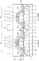
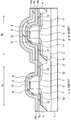
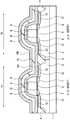
도 1은, 본 발명의 실시예 1인 반도체 장치의 개략구성을 도시하는 모식적인 단면도이고,1 is a schematic sectional view showing a schematic configuration of a semiconductor device according to
도 2는, 드레인 전류변동률의 막응력 의존성을 도시하는 특성도이고,Fig. 2 is a characteristic diagram showing the film stress dependency of the drain current variation rate,
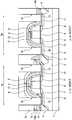
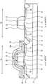
도 3 및 도 4는, 전류방향과 막응력방향과의 관계를 도시하는 모식적 평면도 및 모식적 단면도이고,3 and 4 are schematic plan views and schematic cross-sectional views showing the relationship between the current direction and the film stress direction;
도 5 내지 도 19는, 도 1의 반도체 장치의 제조공정 주에 있어서 모식적 단면도이다.5 to 19 are schematic cross sectional views of the semiconductor device of FIG. 1 during a manufacturing process.
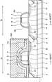
도 20 내지 도 23은, 본 발명을 이루는 과정에서 본 발명자에 의해 발견된 문제점을 설명하기 위한 모식적 단면도이다.20 to 23 are schematic cross-sectional views for explaining the problems found by the present inventors in the process of forming the present invention.
도 1, 도 5 내지 도 19에 있어서, 정면 왼쪽이 n채널 도전형 MISFET(n-ch MISFET)이고, 오른쪽이 p채널 도전형 MISFE(p-ch MISFET)이다.1 and 5 to 19, the front left side is an n-channel conduction type MISFET (n-ch MISFET), and the right side is a p-channel conduction type MISFE (p-ch MISFET).
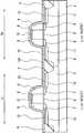
도 1에 도시하는 것과 같이, 본 실시예의 반도체 장치는, 반도체 기판으로서 예를 들면 단결정실리콘으로 이루어지는 p형 실리콘 기판(이하, 간단히 p형 기판이라 한다.)(1)을 주체로 구성되어 있다. p형 기판(1)의 회로형성면(일주면)은 nMIS형성영역(제 1 소자형성영역)(1n) 및 pMIS형성영역(1p)을 갖고, 이 nMIS형성영역(1n)및 pMIS형성영역(1p)은 소자분리영역인 예를 들면 얕은 홈 아이솔레이션(SGI : Shallow Groove Isolation)영역(4)에 의해 서로 면이 구분되어 있다. nMIS형성영역(1n)에는 p형 웰영역(2) 및 n채널 도전형 MISFET(이하, 간단히 n형 MISFET이라 한다.)이 형성되고, pMIS형성영역(1p)에는 n형 웰영역(3) 및 p채널도전 형 MISFET(이하, 간단히 p형 MISFET이라 한다.)이 형성되어 있다. 얕은 홈 아이솔레이션영역(4)은, p형 기판(1)의 회로형성면에 얕은 홈을 형성하고, 그 후, 얕은 홈의 내부에 절연막(예를 들면 질화실리콘막)을 선택적으로 메우므로써 형성된다. 본 실시예의 n형 및 p형 MISFET은, 전류가 p형 기판(1)의 평면방향으로 흐르는 가로형 구조로 되어 있다.As shown in Fig. 1, the semiconductor device of the present embodiment mainly comprises a p-type silicon substrate (hereinafter simply referred to as a p-type substrate) 1 composed of, for example, single crystal silicon. The circuit formation surface (circumferential surface) of the p-
n형 MISFET은, 주로, 채널형성영역, 게이트절연막(5), 게이트전극(6), 사이드 월 스페이서(9), 소스 영역 및 드레인영역을 갖는 구성으로 되어 있다. 소스영역 및 드레인영역은, n형 반도체영역(익스텐션 영역)(7) 및 n형 반도체 영역(10)을 갖는 구성으로 되어 있다. n형 반도체 영역(7)은 게이트전극(6)에 대해 자기정합으로 형성되고, n형 반도체 영역(10)은 게이트전극(6)의 측벽에 설치된 사이드 월 스페이서(9)에 대해 자기정합으로 형성되어 있다. n형 반도체 영역(10)은 n형 반도체 영역(7)보다도 높은 불순물 농도로 형성되어 있다.The n-type MISFET has a structure mainly having a channel formation region, a
p형 MISFET은, 주로, 채널형성영역, 게이트절연막(5), 게이트 전극(6), 사이드 월 스페이서(9), 소스 영역 및 드레인 영역을 갖는 구성으로 되어 있다. 소스 영역 및 드레인 영역은, P형 반도체 영역(익스텐션)(8) 및 p형 반도체 영역(11)을 갖는 구성으로 되어 있다. p형 반도체 영역(8)은 게이트전극(6)에 대해 자기정합으로 형성되고, p형 반도체 영역(11)은 게이트전극(6)의 측벽에 설치된 사이드 월 스페이서(9)에 대해 자기정합으로 형성되어 있다. p형 반도체 영역(11)은 p형 반도체 영역(8)보다도 높은 불순물 농도로 형성되어 있다.The p-type MISFET mainly has a channel formation region, a
게이트전극(6), n형 반도체 영역(10), p형 반도체 영역(11)의 각각의 표면에 는 저저항화를 도모하기 위한 실리사이드층(금속 ·반도체 반응층)(12)이 형성되어 있다 게이트전극(6)의 표면에 설치된 실리사이드층(12), n형 반도체 영역(10) 및 p형 반도체 영역(11)의 표면에 설치된 실리사이드층(12)은, 게이트 전극(6)의 측벽에 설치된 사이드 월 스페이서(9)에 대해 자기정합으로 형성되어 있다. 이들의 실리사이드층(12)은, 예를 들면 살리사이드(Salicide : Self Aligned Silicide)기술에 의해 형성되어 있다. 즉, 본 실시예의 n형 및 p형 MISFET은, 살리사이드구조로 되어 있다.Silicide layers (metal and semiconductor reaction layers) 12 are formed on the surfaces of the
p형 기판(1)의 회로형성면상에는 예를 들면 산화실리콘막으로 이루어지는 층간 절연막(16)이 형성되어 있다. 층간 절연막(16)은, p형 기판(1)의 회로형성면을 덮도록 하여 형성되어 있다. n형 MISFET과 층간 절연막(16) 사이에는 p형 기판(1)의 회로형성면에 인장응력을 발생시키는 막으로서 제 1 질화막인 예를 들면 질화실리콘막(14a)이 형성되어 있다. p형 MISFET과 층간 절연막(16) 사이에는 p형 기판(1)의 회로형성면에 압축응력을 발생시키는 막으로서 제 2 질화막인 예를 들면 질화실리콘막(14b)이 형성되어 있다. 본 실시예에 있어서, 질화실리콘막(14a)은 n형 MISFET상에 그 게이트전극(6)을 덮도록 하여 선택적으로 형성되고, 질화실리콘막(14b)은 p형 MISFET상에 그 게이트전극(6)을 덮도록 하여 선택적으로 형성되어 있다.On the circuit formation surface of the p-
n형 MISFET과 질화실리콘막(14a) 사이에, 및 p형 MISFET과 질화실리콘막(14b) 사이에는, 예를 들면 질화실리콘막으로 이루어지는 절연막(13)이 형성되어 있다. 절연막(13)은, p형 기판(13)은, p형 기판(1)의 회로형성면상에 n형 및 p형 MISFET을 덮도록 하여 형성되어 있다.An insulating
질화실리콘막(14a)과 층간절연막(16) 사이에는, 예를 들면 산화실리콘막으로 이루어지는 절연막(15)이 형성되어 있다. 이 절연막(15)은, 질화실리콘막(14a)상에, 이 질화실리콘막(14a)을 덮도록 하여 선택적으로 형성되어 있다.An insulating
n반도체 영역(10) 및 p형 반도체 영역(11)상에는 층간 절연막(16)의 표면에서 실리사이드층(12)에 도달하는 소스 ·드레인용 콘택트공(18)이 형성되고, 이 소스 ·드레인용 콘택트공(18)의 내부에는 도전성 플러그(19)가 메워져 있다. n반도체 영역(10) 및 p형 반도체 영역(11)은, 실리사이드층(12) 및 도전성 플러그(19)를 개재하고, 층간 절연막(16)상을 연재하는 배선(20)과 전기적으로 접속되어 있다.On the n-
게이트전극(6)상에는 도시하고 있지 않지만, 층간 절연막(16)의 표면에서 실리사이드층(12)에 도달하는 게이트용 콘택트공이 형성되고, 이 게이트용 콘택트공의 내부에는 도전성 플러그(19)가 메워져 있다. 게이트전극(6)은, 실리사이드층(12), 및 게이트용 콘택트공의 내부 도전성 플러그(19)를 개재하고, 층간 절연막916)상을 연재하는 배선(20)과 전기적으로 접속되어 있다.Although not shown on the
소스 ·드레인용 콘택트공(18) 및 게이트용 콘택트공은, 질화실리콘막(14a) 및 (14b)을 에칭 스토퍼막으로 이용하는 SAC(Self Aligned Contact hole)기술에 의해 형성되어 있다. 즉, 질화실리콘막(14a) 및 (14b)는 자기정합 콘택트용 절연막으로 사용되고 있다.The source and drain contact holes 18 and the gate contact holes are formed by a self aligned contact hole (SAC) technique using
질화실리콘막(14a) 및 (14b)는, 예를 들면 플라즈마 CVD(Chemical Vapor Deposition)법에 의해 형성되어 있다. 이 질화실리콘막(14a) 및 (14b)는, 그 형성 조건(반응가스, 압력, 온도, 고주파 전력 등)을 바꾸므로써 p형 기판(1)의 회로형성면에 발생시키는 응력을 제어할 수 있다. 본 실시예에 있어서, 질화실리콘막(14a)은 예를 들면 막형성시의 고주파 전력을 30 ~ 40W로 저전력화하고, p형 기판(1)의 회로형성면에 발생시키는 응력을 인장방향으로 제어한 것이다.The
이렇게 해서 형성된 질화실리콘막(14a)에는 +700 ~ +800MPa 정도의 인장응력이 존재하고, 질화실리콘막(14b)에는 -900 ~ -1000MPa 정도의 압축응력이 존재하기 때문에, n형 MISFET의 채널형성영역에는 인장응력이 발생하고, p형 MISFET의 채널형성영역에는 압축응력이 발생한다. 이 결과, 도 2에 도시하는 것과 같이 질화실리콘막(14a) 및 (14b)를 피막하고 있지 않은 경우와 비교해서, n형 MISFET의 드레인전류는 10 ~ 15% 향상되고, p형 MISFET의 드레인전류는 15 ~ 20%향상됐다. 또한, 이들의 응력은, 앞에서 서술한 것과 같이 주로 채널형성영역을 흐르는 드레인전류(Id)의 방향(게이트길이방향)과 동일방향으로 걸린다.The
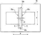
여기에서, MISFET의 채널형성영역에 발생하는 응력에 관해, 간략한 도 및 본 실시예와 일부 다른 부호를 이용하여 설명한다. 도 3 및 도 4에 도시하는 MISFET은 본 실시예와 동일하게 살리사이드구조로 되어 있고, 부호 30는 MISFET의 채널형성영역, 부호 31는 채널형성영역(30)을 흐르는 드리엔전류의 방향, 부호 32는 게이트전극(6)에 정합하여 형성된 반도체 영역, 부호 33은 사이드 월 스페이서(9)에 정합하여 형성된 반도체 영역, 부호 34는 채널형성영역(30)에 응력을 발생시키기 위한 막, 부호, 35a 및 35b는 단차부이다. Here, the stress generated in the channel forming region of the MISFET will be described using a simplified diagram and some symbols different from the present embodiment. The MISFET shown in Figs. 3 and 4 has the same salicide structure as in the present embodiment, where 30 is the channel formation region of the MISFET, 31 is the direction of the driene current flowing through the
도 3 및 도 4에 도시하는 것과 같이 MISFET은 게이트전극(6)의 측벽에 게이 트전극(6)을 둘러싸듯이 하여 사이드 월 스페이서(9)가 설치된 구조로 되어 있다. 게이트전극(6) 및 사이드 월 스페이서(9)는 기판에서 돌출되어 있기 때문에, 게이트전극(6) 및 사이드 월 스페이서(9)에 의한 단차부(35a, 35b)가 형성되어 있다. 이러한 구조의 MISFET상에, 그 게이트전극(6)을 덮도록 하고, 채널형성영역(30)에 응력(인장응력, 혹은 압축응력)을 발생시키는 막(34)을 형성한 경우, 게이트길이방향(X)에 있어서 단차부(35a)의 최하부 및 게이트폭방향(Y)에 있어서 단차부(35b)의 최하부에 막(34)에 의한 응력이 집중하기 때문에, 게이트길이방향(X)에 있어서 단차부(35a)의 최하부를 기점으로 하는 게이트길이방향의 막응력이 채널형성영역(30)에 작용함과 동시에, 게이트폭방향(Y)에 있어서 단차부(35b)의 최하부를 기점으로 하는 게이트폭방향의 막응력이 채널형성영역(30)에 작용한다. 즉, 막(34)에 의한 응력이 인장응력인 경우는, 채널형성영역(30)에 게이트길이방향 및 게이트폭방향의 인장응력이 발생하고, 막(34)에 의한 응력이 압축응력인 경우는, 채널형성영역(30)에 게이트길이방향 및 게이트폭방향의 압축응력이 발생한다.As shown in Figs. 3 and 4, the MISFET has a structure in which the
그러나, 게이트전극(6)의 게이트길이방향(X)에 있어서의 길이는, 그 게이트폭방향(Y)에 있어서의 길이와 비교하여 압도적으로 작으므로, 게이트폭방향(Y)에 있어서 단차부(35b)의 최하부에 집중하는 인장응력, 혹은 압축응력에 의해 채널형성영역(30)에 발생하는 게이트폭방향의 인장응력, 혹은 압축응력은 극히 작다. 따라서, 막(34)에 의해 채널형성영역(30)에 발생하는 응력은, 실질적으로, 게이트길이방향의 인장응력, 혹은 압축응력, 바꿔 말하면 드레인전류방향(31)에 따른 인장응력, 혹은 압축응력만으로 간주할 수 있다.However, since the length of the
p형 MISFET에 있어서는, 채널형성영역(30)에 게이트폭방향의 압축응력을 건 경우, 드레인전류는 감소한다고 보고되어 있다. 막(34)에 의한 채널형성영역(30)의 응력제어에서는, 앞에서 서술한 것과 같이 채널형성영역(30)에 발생하는 게이트폭방향의 압축응력은 극히 작으므로, p형 MISFET의 드레인전류증가를 효율적으로 행할 수 있다. 따라서, 막(34)에 의한 채널형성영역(30)의 응력제어는, p형 전계효과 트랜지스터에 대해 특히 유효하다.In the p-type MISFET, when the compressive stress in the gate width direction is applied to the
또한, 막(34)의 응력에 의해 채널형성영역(30)에 발생하는 응력은, 막응력의 기점이 채널형성영역(30)에서 떨어짐(멀어짐)에 따라 감소하므로, 막응력의 기점은 가능한 한 채널형성영역(30)에 근접하는 것이 바람직하다. 앞에서 서술한 설명에서는, 게이트전극(6) 및 사이드 월 스페이서(9)에 의한 단차부(35a, 35b)의 최하부가 막응력의 기점이 되지만, 사이드 월 스페이서(9)를 갖지 않는 MISFET의 경우는, 게이트전극(6)의 측벽 최하부가 막응력의 기점이 된다.In addition, since the stress generated in the
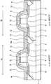
다음으로, 본 실시예 1의 반도체 장치의 제조에 관해, 도 5 내지 도 19를 이용하여 설명한다.Next, manufacturing of the semiconductor device of the first embodiment will be described with reference to FIGS. 5 to 19.
우선, 비저항 10Ωcm를 갖는 단결정실리콘으로 이루어지는 p형 기판(1)을 준비하고, 그 후, 도 5에 도시하는 것과 같이 p형 기판(1)의 회로형성면에 p형 웰영역(2) 및 n형 웰영역(3)을 선택적으로 형성한다.First, a p-
다음으로, 도 5에 도시하는 것과 같이 p형 기판(1)의 회로형성면에 nMIS형성영역(제 1의 소자형성영역)(1n) 및 pMIS형성영역(제 2 소자형성영역)(1p)을 구획하는 소자분리영역으로서, 얕은 홈 아이솔레이션영역(4)을 형성한다. 이 얕은 홈 아 이솔레이션영역(4)은, p형 기판(1)의 회로형성면에 얕은 홈(예를 들면 300[nm]정도의 깊이의 홈)을 형성하고, 그 후, p형 기판(1)의 회로형성면상에 예를 들면 산화실리콘막으로 이루어지는 절연막을 CVD법으로 형성하고, 그 후, 절연막이 얕은 홈 내부만 남도록 CMP(화학적 기계연마 : Chemical Mechanical Polishing)법으로 평탄화하므로써 형성된다.Next, as shown in FIG. 5, the nMIS formation region (first element formation region) 1n and the pMIS formation region (second element formation region) 1p are formed on the circuit formation surface of the p-
다음으로, 도 6에 도시하는 것과 같이 열처리를 실시하고 p형 기판(1)의 회로형성면의 nMIS형성영역(1n) 및 pMIS형성영역(1p)에 예를 들면 두께가 2 ~ 3nm정도의 산화실리콘막으로 이루어지는 게이트절연막(5)을 형성하고, 그 후, p형 기판(1)의 회로형성면상의 전면에 예를 들면 150 ~ 200nm정도의 두께의 다결정실리콘막을 CVD법으로 형성하고, 그 후, 다결정 실리콘막에 패터닝을 실시하여 게이트전극(6)을 형성한다. 다결정실리콘막에는 저항치를 저감하는 불순물이 그 퇴적중 또는 퇴적후에 도입된다.Next, as shown in FIG. 6, heat treatment is performed to oxidize the
다음으로, 도 6에 도시하는 것과 같이 게이트전극(6)이 형성되어 있지 않은 p형 웰영역(2)의 부분에 불순물로서 예를 들면 비소(As)를 이온투입법으로 선택적으로 도입하여 한쌍의 n형 반도체 영역(익스텐션영역)(7)을 형성하고, 그 후, 게이트전극(6)이 형성되어 있지 않은 n형 웰영역(3)의 부분에 불순물로써 예를 들면 이불화붕소(BF2)를 이온투입법으로 선택적으로 도입하여 한쌍의 p형 반도체 영역(익스텐션영역)(8)을 형성한다. n형 반도체 영역(7) 형성은, pMIS형성영역(1p)을 포토레지스토 마스크로 덮은 상태로 행한다. 또, p형 반도체 영역(8)의 형성은, nMIS형성 영역(1n)을 포토레지스토 마스크로 덮은 상태에서 행한다. 비소의 도입은, 가속에너지 1 ~ 5KeV, 도즈량 1 ~ 2 ×10¹⁵/cm2의 조건에서 행한다. n형 반도체 영역(7) 및 p형 반도체 영역(8)은 게이트전극(6)에 정합하여 형성된다.Next, as shown in FIG. 6, arsenic (As), for example, as an impurity is selectively introduced into a portion of the p-
또한, 불순물을 도입하여 반도체 영역(7, 8)을 형성한 후, 이 반도체 영역(7, 8)을 활성화하는 열처리가 실시된다.In addition, after the impurity is introduced to form the
다음으로, 도 6에 도시하는 것과 같이 게이트전극(6)의 측벽에 예를 들면 게 이트길이방향의 막두께가 50 ~ 70nm 정도의 사이드 월 스페이서(9)를 형성한다. 사이드 월 스페이서(9)는 p형 기판(1)의 회전형성면상의 전면에 예를 들면 질화실리콘막 또는 질화실리콘막으로 이루어지는 절연막을 CVD법으로 형성하고, 그 후, 절연막에 RIE(Reactive Ion Etching) 등의 이방성 에칭을 실시하므로써 형성된다. 사이드 월 스페이서(9)는 게이트전극(6)에 정합하여 형성된다.Next, as shown in FIG. 6,
다음으로 도 6에 도시하는 것과 같이 게이트전극(6) 및 사이드 월 스페이서(9)가 형성되어 있지 않은 p형 웰 영역(2)의 부분에 불순물로서 예를들면 비소(As)를 이온투입법으로 선택적으로 도입하여 한쌍의 n형 반도체 영역(10)을 형성하고, 그 후, 게이트전극(6) 및 사이드 월 스페이서(9)가 형성되어 있지 않은 n형 웰 영역(3)의 부분에 불순물로서 예를 들며 이불화붕소를 이온투입법으로 선택적으로 도입하여 한쌍의 p형 반도체 영역(11)을 형성한다. n형 반도체 영역(10)의 형성은, pMIS형성영역(1)P)를 포토레지스트 마스크로 덮은 상태에서 행한다. 또, p형 반도체 영역(11)의 형성은, nMIS형성영역(1n)을 포토레지스트 마스크로 덮은 상 태에서 행한다. 비소의 도입은, 가속에너지 35 ~ 45KeV, 도즈량 2 ~ 4 ×10¹⁵/cm2의 조건에서 행한다. 또, 이불화붕소의 도입은, 가속에너지 40 ~ 50KeV, 도즈량 2 ~ 4 ×10¹⁵/cm2의 조건에서 행한다. n형 반도체 영역(10) 및 p형 반도체 영역(11)은, 사이드 월 스페이서(9)에 정합하여 형성된다.Next, as shown in FIG. 6, for example, arsenic (As) as an impurity in the portion of the p-
또한, 불순물을 도입하여 반도체 영역(10, 11)을 형성한 후, 이 반도체 영역(10, 11)을 활성화하기 위한 열처리가 실시된다.After the impurity is introduced to form the
이 공정에 있어서, 게이트전극(6)에 정합하여 형성된 n형 반도체 영역(7) 및 사이드 월 스페이서(9)에 정합하여 형성된 n형 반도체 영역(10)을 갖는 소스 영역 및 드레인 영역이 형성된다. 또, 게이트전극(6)에 정합하여 형성된 p형 반도체 영역(8) 및 사이드 월 스페이서(9)에 정합하여 형성된 p형 반도체 영역(11)을 갖는 소스영역 및 드레인영역이 형성된다. 또, 가로형 n형 및 p형 MISFET이 형성된다.In this step, a source region and a drain region having an n-
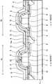
다음으로, 자연산화막 등을 제거하여 게이트전극(6) 및 반도체 영역(10, 11)의 표면을 노출시킨 후, 도 7에 도시하는 것과 같이, 이들의 표면상을 포함하는 P형 기판(1)의 회로형성면상의 전면에 고융점 금속막으로서 예를 들면, 코발트(Co)막(12a)을 스퍼터법으로 형성하고, 그 후, 도 8에 도시하는 것과 같이 열처리를 실시하고, 게이트전극(6)의 실리콘(Si)과 코발트막(12a)의 Co를 반응시켜서 게이트전극(6)의 표면에 금속 ·반도체 반응층인 실리사이드(CoSix)층(12)을 형성함과 동시에, 반도체 영역(10, 11)의 Si와 코발트막(12a)의 Co를 반응시켜서 반도체 영역(10, 11)의 표면에 실리사이드(CoSix)층(12)을 형성하고, 그 후, 도 9에 도시 하는 것과 같이, 실리사이드층(12)이 형성된 영역 이외의 미반응 코발트막(12a)을 선캑적으로 제거하고, 그 후, 열처리를 실시하여 실리사이드층(12)을 활성화한다.Next, after removing the native oxide film or the like to expose the surfaces of the
이 공정에 있어서, 게이트전극(6)의 표면에 설치된 실리사이드층(12) 및 반도체 영역(10, 11)의 표면에 설치된 실리사이드층(12)은 사이드 월 스페이서(9)에 정합하여 형성된다. 또, 실리사이드구조의 n형 및 p형 MISFET이 형성된다.In this step, the
다음으로, 도 10에 도시하는 것과 같이 n형 및 p형 MISFET상을 포함하는 p형 기판(1)의 회로형성면상의 전면에 예를 들면 5 ~ 10nm 정도의 두께의 산화실리콘막으로 이루어지는 절연막(13)을 CVD1법으로 형성한다. 이 공정에 있어허, 게이트2전극(6)의 실리사이드층(12), 반도체 영역(10, 11)의 실리사이드층(12), 및 사이드 월 스페이서(9) 등은, 절연막(13)에서 덮인다.Next, as shown in FIG. 10, an insulating film made of a silicon oxide film having a thickness of about 5 to 10 nm, for example, on the entire surface of the p-
다음으로, 도 11에 도시하는 것과 같이, n형 MISFET상을 포함하는 p형 기판(1)의 회로형성면상의 전면에, 절연막으로서 예를 들면 100 ~ 120nm 정도의 두께의 질화실리콘막(14a)을 플라즈마 CVD법으로 형성한다. 질화실리콘막(14a)의 형성은, 예를 들면 고주파전력 350 ~ 400W, 혹은 챔버내 압력 300 ~ 350Torr의 조건에서 행한다.Next, as shown in FIG. 11, the
그 공정에 있어서, n형 및 p형 MISFET은, 질화실리콘막(14a)으로 덮인다. 또, 게이트전극(6)의 실리사이드층(12), 반도체 영역(10, 11), 및 사이드 월 스페이서(9) 등은, 절연막(13)을 개재하여 질화실리콘막(14a)으로 덮인다.In this step, the n-type and p-type MISFETs are covered with the
다음으로, 도 12에 도시하는 것과 같이 n형 및 p형 MISFET상을 포함하는 p형 기판(1)의 회로형성면상의 전면에, 예를 들면 50nm 정도의 두께의 산화실리콘막으 로 이루어지는 절연막(15)을 CVD법으로 형성한다. 이 공정에 있어서, 질화실리콘막(14a)은, 절연막(15)으로 덮인다.Next, as shown in FIG. 12, the insulating
다음으로, 도 13에 도시하는 것과 같이, 절연막(15)상에 nMIS형성영역(1n)(n형 MISFET)상을 선택적으로 덮는 포토레지스트 마스크(RM1)을 형성한다.Next, as shown in FIG. 13, the photoresist mask RM1 which selectively covers the nMIS formation area |
다음으로, 포토레지스트 마스크(RM1)를 에칭 마스크로 하여 에칭처리를 실시하고, 도 14에 도시하는 것과 가티 pMIS형성영역(1p)상(p형 MISFET상)의 절연막(15), 및 질화실리콘막(14a)을 순차제거한다. 절연막(15)의 가공은 웨트 에칭으로 행하고, 질화실리콘막(14a)의 가공은 등방성 드라이 에칭으로 행한다.Next, the etching process is performed using the photoresist mask RM1 as an etching mask, and the insulating
이 공정에 있엇, n형 MISFET상에 그 게이트전극(6)을 덮도록 하여 질화실리콘막(14a)이 선택적으로 형성된다. 이렇게 해서 질화실리콘막(14a)을 선택적으로 형성하므로써, 질화실리콘막(14a)에 의해 n형 MISFET의 채널형성영역에 인장응력을 선택적으로 발생시킬 수 있다.In this step, the
또, 이 공정에 있어서, p형 MISFET에서는, 게이트전극(6)의 표면 실리사이드층(12), p형 반도체 영역(11)의 표면의 실리사이드층(12), 및 사이드 월 스페이서(9)가 절연막(13)에 의해 덮여 있기 때문에, 이들의 실리사이드층(12) 및 사이드 월 스페이서(9)가 질화실리콘막(14a)의 가공시의 오버 에칭에 의해 깎여버리는 불합리함을 억제할 수 있다. 즉, 절연막(13)은, 질화실리콘막(14a)의 가공시에 있어서 에칭 스토퍼의 역할을 한다.In this step, in the p-type MISFET, the
또한, 이 공정에 있어서, 절연막(13)이 존재하지 않았던 경우, 질화실리콘막(14a)의 가공시의 오버 에칭에 의해 문제가 발생한다. 이 문제에 관해 서는 나중에 상세하게 설명한다.In addition, in this process, when the insulating
다음으로, 포토레지스트 마스크(RM1)을 제거한 후, 도 15에 도시하는 것과 같이 절연막(15)상을 포함하는 p형 기판(1)의 회로형성면상의 전면에, 절연막으로서 예를 들면 100nm 정도의 두께의 질화실리콘막(14b)을 플라즈마 CVD법으로 형성한다. 질화실리콘막(14b)의 형성은, 예를 들면 고주파전력 600 ~ 700W, 혹은 챔버내 압력 5 ~ 10Torr의 조건으로 행한다.Next, after removing the photoresist mask RM1, as shown in FIG. 15, the entire surface on the circuit formation surface of the p-
이 공정에 있어서, n형 및 p형 MISFET은, 질화실리콘막(14b)으로 덮인다. 또, n형 MISFET상의 질화실리콘막(14a)은 절연막(15)을 개재하여 질화실리콘막(14b)으로 덮인다.In this step, the n-type and p-type MISFETs are covered with the
다음으로, 도 16에 도시하는 것과 같이 질화실리콘막(14b)상에, pMIS형성영역(1p)(p형 MISFET)상을 선택적으로 덮는 포토레지스트 마스크(RM2)를 형성한다.Next, as shown in FIG. 16, a photoresist mask RM2 is formed on the
다음으로, 포토레지스트 마스크(RM2)를 에칭 마스크로 하여 에칭처리를 실시하고, 도 17에 도시하는 것과 같이, nMIS형성영역(1n상)(n형 MISFET상)의 질화실리콘막(14b)를 제거한다. 질화실리콘막(14b)의 가공은 등방성 드라이 에칭으로 행한다.Next, an etching process is performed using the photoresist mask RM2 as an etching mask, and the
이 공정에 있어서, p형 MISFET상에 그 게이트전극(6)을 덮도록 하여 질화실리콘막(14b)가 선택적으로 형성된다. 이렇게 해서 질화실리콘막(14b)을 선택적으로 형성하므로써, 질화실리콘막(14b)에 의해 p형 MISFET의 채널형성영역에 압축응력을 선택적으로 발생시킬 수 있다.In this step, the
또, 이 공정에 있어서, n형 MISFET상의 질화실리콘막(14a)은 절연막(15)에 의해 덮여있기 때문에, 이 질화실리콘막(14a)이 질화실리콘막(14b)의 가공시으 오버 에칭에 의해 깎여버리는 불합리함을 억제할 수 있다. 즉, 절연막(15)은, 질화실리콘막(14b)의 가공시에 있어서 에칭 스토퍼의 역할을 한다.In this step, since the
다음으로, 포토레지스트 마스크(RM2)를 제거한 후, 도 18에 도시하는 것과 같이 n형 및 p형 MISFET상을 포함하는 P형 기판(1)의 회로형성면상의 전면에 예를 들면 산화실리콘막으로 이루어지는 층간 절연막(16)을 플라즈마 CVD법으로 형성하고, 그 후, 층간절연막(16)의 표면을 CMP법으로 평탄화한다.Next, after the photoresist mask RM2 is removed, a silicon oxide film is formed on the entire surface on the circuit formation surface of the P-
다음으로, 도 18에 도시하는 것과 같이, 층간절연막(16) 중에, Ar, Ge, Si, As, Sb, In, BF2 등으 불순물(17)을 이온투입법으로 도입하고, 층간절연막(16) 중의 결정성을 파괴한다. 이 공정에 있엇, 층간절연막(16)의 응력이 완화되기 때문에, 층간절연막(16)의 응력이 MISFET의 채널형성영역에 작용하는 영향을 억제할 수 있다. 또한, 층간절연막(16)의 단면을 관찰하면 명백하게 파괴된 흔적이 남는다.Next, as shown in FIG. 18, in the
다음으로, 도 19에 도시하는 것과 같이, 반도체 영역(11, 12)상에, 층간절연막(16)의 표면에서 실리사이드층(12)에 도달하는 소스 ·드레인용 콘택트공(18)을 형성한다. 소스 ·드레인용 콘택트공918)의 형성은, 질화실리콘막(14a, 14b)을 에칭 스토퍼로 하는 SAC기술로 행한다. 구체적으로는 우선, 반도체 영역(10, 11)과 대향하는 위치에 콘택트공용의 개구패턴을 갖는 포토레지스트 마스크를 층간절연막(16)상에 형성하고, 그 후, 상기 포토레지스트 마스크를 에칭 마스크로 하고, 층간절연막(16), 절연막(15), 질화실리콘막(14a, 14b) 및 절연막(13)에 이방 성 드라이 에칭을 순차적으로 실시한다. 층간절연막(16) 및 절연막(15)의 에칭은, 질화실리콘막(14a, 14b)에 대해 선택비를 취할 수 있는 조건으로 행한다. 질화실리콘막(14a, 14b)의 에칭은, 절연막(13)에 대해 선택비를 취할 수 있는 조건으로 행한다. 절연막(13)의 에칭은, 실리사이드층(12), 및 p형 기판(1)에 대해 선택비를 취할 수 있는 조건으로 행한다. 또한, 절연막(13)의 에칭은, 질화실리콘막(14a, 14b)의 가공시의 오버 에칭으로 행해도 좋다.Next, as shown in FIG. 19, source and drain contact holes 18 reaching the
다음으로, 도시하고 있지 않지만, 소스 ·드레인용 콘택트공(18)의 형성과 동일한 방법으로, 게이트전극(6)상에 층간절연막(16)의 표면에서 실리사이드층(12)에 도달하는 게이트용 콘택트공을 형성한다.Next, although not shown, the gate contact reaching the
다음으로, 소스 드레인용 콘택트공(18)의 내부, 및 게이트용 콘택트공의 내부에 금속 등의 도전물을 메워서 도전성 플러그(19)를 형성하고, 그 후, 층간절연막(16)상에 배선(20)을 형성하므로써, 도 1에 도시하는 구조가 된다.Next, a
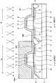
다음으로, 본 발명을 이루는 과정에서 본 발명자가 발견한 문저점과 함께 본 발명에 관해 설명한다.Next, the present invention will be described together with the vertexes found by the present inventors in the process of forming the present invention.
p형 MISFET상의 질화실리콘막(14a)을 이방성 드라이 에칭으로 제거한 경우, 이방성 드라이 에칭으로서는 사이드 월 스페이서(9)의 측벽을 따라 질화실리콘막(14a)부분의 막두께가 실행적으로 두껍게 보이기 때문에, 도 20에 도시하는 것과 같이 사이드 월 스페이서(9)의 측벽에 질화실리콘막(14a)의 일부가 잔존한다. 이대로의 상태에서, pMISFET상에 질화실리콘막(14b)을 형성한 경우, 도 21에 도시하는 것과 같이 게이트전극(6), 사이드 월 스페이서(9) 및 일부 질화실리콘 막(14a)에 의한 단차부(35a)의 최하부에 질화실리콘막(14b)의 응력이 집중하기 때문에, 질화실리콘막(14b)의 응력의 기점이 사이드 월 스페이서(9)의 측벽에 잔존하는 질화실리콘막(14a)에 의해 p형 MISFET의 채널형성영역에서 떨어져 버리고, 질화실리콘막(14b)의 막응력에 의해 채널형성영역에 압축응력을 발생시키는 효과가 감소해버린다. 또, 반대의 응력작용을 갖는 질화실리콘막(14a)이 사이드 월 스페이서(9)의 측벽에 잔존하기 때문에, 질화실리콘막(14b)에 의해 채널형성영역에 압축응력을 발생시키는 효과가 더 감소해버린다. 따라서, p형 MISFET상의 질화실리콘막(14a)의 제거에서는, 단차부에 에칭잔여물이 발생하지 않는 등방성 드라이 에칭으로 행하는 것이 유효하다.In the case where the
그러나, p형 MISFET상의 질화실리콘막(14a)을 등방성 드라이 에칭으로 제거한 경우, 새로운 문제가 발생한다.However, when the
질화실리콘막의 등방성 드라이 에칭으로서는, 일반적으로 CF4 또는 CF6 등의 불화가스를 이용한 등방성 플라즈마 에칭이 사용되고 있다. 이 등방성 플라즈마 에칭에서는, 산화실리콘막과 실리사이드층에 대해서는 선택비를 취할 수 있지만, 실리콘에 대해서는 선택비를 취할 수 없다.As isotropic dry etching of the silicon nitride film, isotropic plasma etching using fluorinated gas such as CF4 or CF6 is generally used. In this isotropic plasma etching, the selectivity can be taken for the silicon oxide film and the silicide layer, but cannot be taken for silicon.
산화실리콘막으로 이루어지는 사이드 월 스페이서(9)는 질화실리콘막(14a)의 등방성 플라즈마 에칭에 대해 선택성을 갖지만, 질화실리콘막(14a)의 가공시의 오버 에칭에 의해 약간 에칭되기 때문에, 사이드 월 스페이서(9)의 존체 막두께가 게이트전극(6)을 향해 후퇴한다. 한편, p형 반도체 영역(11)의 표면 실리사이드층(12)은 사이드 월 스페이서(9)에 정합하여 형성되어 있다. 따라서, 질화실리콘막(14a)의 가공시의 오버 에칭에 의한 사이드 월 스페이서(9)의 후퇴에 의해. 도 22에 도시하는 것과 같이, 사이드 월 스페이서(9)와 실리사이드층(12) 사이에 실리콘의 노출부(1a)가 형성되어 버린다. 질화실리콘막의 등방성 플라즈마 에칭은, 실리콘에 대해 선택비를 취할 수 없기 때문에, 질화실리콘막(14a)의 가공시의 오버 에칭에 의해 노출부(1a)에서 p형 기판(1)이 깎여버리고, 게이트전극(6)이 벗겨지는 등의 불합리한 점이 발생해버린다.The
또, 실리사이드층(12)은, 질화실리콘막(14a)의 등방성 플라즈마 에칭에 대해 선택성을 갖지만, 질화실리콘막(14a)의 가공시의 오버 에칭에 의해 약간 에칭되기 때문에, 실리사이드층(12)의 막두께가 얇아진다. 실리사이드층(12)은, MISFET의 미세화에 따라 게이트저항의 증가와 소스 ·드레인저항의 증가를 억제하기 위해, 게이트전극(6)의 표면과 P형 반도체 영역(11)의 표면에 설치되어 있다. 따라서, 질화실리콘막(14a)의 가공시의 오버 에칭에 의해 실리사이드층(12)의 막두께가 얇아지면, MISFET의 미세화에 동반하는 게이트저항의 증가와 소스 ·드레인저항의 증가를 억제하는 효과가 감소되어 버린다.The
또, 살리사이드구조의 p형 MISFET의 경우는, 실리사이드층(12)이 에칭 스토퍼의 역할을 하기 때문에, 게이트전극(6)에 있어서는 실리사이드층(12)하의 다결정 실리콘막, 소스영역 및 드레인영역에 있어서는 실리사이드층(12)하의 p형 반도체영역(11)이 질화실리콘막(14a)의 가공시의 오버 에칭에 의해 깎여버리는 일은 없지만, 게이트전극(6)의 표면과 p형 반도체영역(11)의 표면에 실리사이드층(12)을 갖 지 않는 구조의 경우는 도 23에 도시하는 것과 같이 게이트전극(6)의 다결정 실리콘막, 소스영역 및 드레인영역의 p형 반도체 영역(11)이 깎여버리고, 이들의 두께가 감소해버리기 때문에. 게이트저항 및 소스 ·드레인저항의 증가는 전류구동능력의 저하를 불러일으킨다.In the case of the p-type MISFET having a salicide structure, since the
따라서, p형 MISFET상의 질화실리콘막(14a)의 제거는, 단추부에 에칭잔여물이 발생하지 않는 등방성 드라이 에칭으로 행해지는 것이 유효하지만, 질화실리콘막(14a)의 가공을 등방성 드라이에칭으로 행하기 위해서는, 앞에서 서술한 문제를 해결할 필요가 있다.Therefore, it is effective to remove the
본 발명자의 검토에 따르면, 사이드 월 스페이서(9)의 후퇴에 관한 문제는, n형 및 p형 MISFET상에, 이들의 게이트전극(6)을 덮도록 하여 질화실리콘막(14a)을 형성하기 전에, 적어도 p형 반도체 영역(11)에 있어서 실리사이드층(12)의 사이드 월 스페이서측 단부상을 에칭 스토퍼로서 기능하는 절연막으로 덮어두므로써 해결할 수 있다.According to the inventor's review, the problem concerning the retreat of the
또, 실리사이드층(12)의 깎임에 관한 문제는, n형 MISFET상에 이들의 게이트전극(6)을 덮도록 하여 질화실리콘막(14a)을 형성하기 전에 실리사이드층(12)의 전체를 에칭 스토퍼로서 기능하는 절연막으로 덮어두므로써 해결할 수 있다.In addition, the problem related to shaving of the
또, 실리사이드층(12)을 갖지 않는 구조에 관한 문제는, n형 및 p형 MISFET상에 이들의 게이트전극(6)을 덮도록 하여 질화실리콘막(14a)을 형성하기 전에, 게이트전극(6)의 표면과 p형 반도체영역(11)의 표면을 에칭 스토퍼로서 기능하는 절연막으로 덮어두므로써 해결할 수 있다.In addition, the problem regarding the structure without the
절연막으로서는, 질화실리콘막(14a)의 등방성 플라즈마 에칭에 대해 선택성을 갖는 것, 예를 들면 산화실리콘막이 바람직하다.As the insulating film, one having selectivity with respect to isotropic plasma etching of the
앞에서 서술한 실시예 1에서는, 도 10 및 도 11에 도시하는 것과 같이, 질화실리콘막(14a)을 형성하기 전에, 산화실리콘막으로 이루어지는 절연막(13)을 CVD법으로 형성하고 있다. CVD법, 즉 퇴적법으로 절연막(13)을 형성하는 경우, p형 MISFET상에 있어서, 게이트전극(6)의 표면 실리사이드층(12), p형 반도체 영역(11)의 표면 실리사이드층(12), p형 반도체 영역(11)의 표면에 있어서 실리사이드층(12)의 사이드 월(9)측의 단부, 및 사이드 월 스페이서(9)를 절연막(13)으로 덮을 수 있다.In Example 1 mentioned above, the insulating
따라서, p형 MISFET상의 질화실리콘막(14b)의 제거는, 도 14에 도시하는 것과 같이, 게이트전극(6)의 표면 실리사이드층(12), p형 반도체 영역(11)의 표면 실리사이드층(12), p형 반도체 영역(11)의 표면에 있어서 실리사이드층(12)의 사이드 월(9)측 단부, 및 사이드 월 스페이서(9)를 절연막(13)으로 덮은 상태에서 이루어지기 때문에, 사이드 월 스페이서(9)의 후퇴에 관한 문제, 실리사이드층(12)의 깎임에 관한 문제를 한번에 해결할 수 있다.Therefore, the removal of the
이렇게, 본 실시예 1에 따르면, n형 MISFET의 채널형성영역에 인장응력, p형 MISFET의 채널형성영역에 압축응력이 따로따로 부여된 결과, n형 MISFET 및 p형 MSIFET의 각 채널형성영역에 작용하는 응력의 크기에 따라, n형 MISFET 및 p형 MISFET으로 같이 드레인전류가 증가한다.Thus, according to the first embodiment, as a result of separately applying tensile stress to the channel forming region of the n-type MISFET and compressive stress to the channel forming region of the p-type MISFET, the channel forming regions of the n-type MISFET and the p-type MSIFET are separately provided. Depending on the magnitude of the stress acting, the drain current increases with both the n-type and p-type MISFETs.
또, n형 MISFET 및 p형 MISFET의 채널형성영역에 작용하는 응력을 개별로 제 어할 수 있기 때문에, n형 MISFET과 p형 MISFET의 드레인전류비를 자유롭게 제어할 수 있다.In addition, since the stresses acting on the channel forming regions of the n-type MISFET and the p-type MISFET can be individually controlled, the drain current ratio of the n-type MISFET and the p-type MISFET can be freely controlled.
또, n형 MISFET 및 p형 MISFET의 드레인전류를 동시에 증가시킬 수 있으므로, n형 및 p형 MISFET을 갖는 반도체장치의 고속화를 도모할 수 있다.In addition, since the drain currents of the n-type MISFET and the p-type MISFET can be increased at the same time, the semiconductor device having the n-type and p-type MISFETs can be increased in speed.
또, p형 MISFET상의 질화실리콘막(14a)으 등방성 드라이 에칭으로 제거할 때에 발생하는, 사이드 월 스페이서(9)의 후퇴에 관한 문제와 실리사이드층(12)의 깎임에 관한 문제를 해결할 수 있으므로, 제조수득률 및 신뢰성이 높은 반도체 장치를 제공할 수 있다.In addition, since the problems related to the retraction of the
또한, 질화실리콘막의 형성방법을 바꾸어 막응력을 바꾸는 방법으로서는, 상기 실시예의 고주파전력을 바꾸는 방법 외에, 하기의 방법을 들 수 있다.As the method of changing the film stress by changing the method of forming the silicon nitride film, the following method can be mentioned in addition to the method of changing the high frequency power of the above embodiment.
(1) 원료가스를 바꾸는 방법으로서, 질화실리콘막(14a)의 형성에는 SiH4와 NH3와 N2를 사용하고, 질화실리콘막(14b)의 형성에는 NH3를 제외하고 SiH4와 N2를 사용한다.(1) As a method of changing the source gas, SiH4 and NH3 and N2 are used to form the
(2) 형성온도를 바꾸는 방법으로서, 질화실리콘막(14b)의 형성시보다도, 질화실리콘막(14a)의 형성시 온도를 높게 한다.(2) As a method of changing the formation temperature, the temperature at the time of formation of the
(3) 압력을 바꾸는 방법으로서, 질화실리콘막(14b)의 형성시보다도, 질화실리콘막(14a)의 형성시 압력을 높게 한다.(3) As a method of changing the pressure, the pressure at the time of forming the
등이다. 물론, 상기 중 어느 조합을 복합시켜도 좋다. 요는 어떻게 질화실리콘막(14a)을 인장응력측에, 질화실리콘막(14b)을 압축응력측으로 하는가가 중요하 다.And so on. Of course, you may combine any of the above combinations. In other words, it is important how the
또, 매엽열 CVD법을 이용한 질화막의 형성방법으로서는, 막형성시의 압력을 낮추는 만큼, 또 온도를 높게 하는 만큼 막응력을 인장측으로 할 수 있고, 질화실리콘막(14a)에 최적이다.As the method of forming the nitride film using the sheet heat CVD method, the film stress can be set to the tensile side as much as the pressure at the time of film formation is lowered and the temperature is increased, which is optimal for the
도 24는, 본 발명의 실시예 1의 변형예인 반도체 장치의 제조공정 중에 있어서, 모식적 단면도이다. 도 24에 있어서, 대향하여 왼쪽이 n형 MISFET이고, 오른쪽이 p형 MISFET이다.24 is a schematic sectional view of the semiconductor device during a manufacturing step of Modification Example 1 of the present invention. In Fig. 24, the left side is an n-type MISFET and the right side is a p-type MISFET.
앞에서 서술한 실시예 1에서는, 질화실리콘막(14b)보다도 먼저 질화실리콘막(14a)을 형성하는 예에 관해 설명했지만, 도 24에 도시하는 것과 같이, 질화실리콘막(14a)보다도 먼저 질화실리콘막(14b)을 형성해도 좋다. 이러한 경우에 있어서도, n형 MISFET의 채널형성영역에 인장응력, p형 MISFET의 채널형성영ㅇ역에 압축응력을 따로따로 부여할 수 있기 때문에, n형 및 p형 MISFET의 드레인전류를 동시에 증가할 수 있다.In Example 1 described above, an example in which the
또, n형 MISFET상의 질화실리콘막(14b)을 등방성 플라즈마 에칭으로 제거할 때. 게이트전극(6)의 표면 실리사이드층(12), n형 반도체 영역(10)의 표면 실리사이드층(12), n형 반도체 영역(10)의 표면에 있어서 실리사이드층(12)의 사이드 월(9)측 단부, 및 사이드 월 스페이서(9)를 절연막(13)으로 덮은 상태에서 행하므로써, 사이드 월 스페이서(9)의 후퇴에 관한 문제, 실리사이드층(12)의 깎임에 관한 문제를 발생시키는 일 없이, n형 MISFET상의 질화실리콘막(14b)을 등방성 플라즈마 에칭으로 제거할 수 있다.When the
또한, 실시예 1 및 그 변형예에서는, 산화실리콘막으로 이루어지는 절연막(13)을 질화실리콘막(14a)의 가공시의 에칭 스토퍼로 이용한 예에 관해 설명했지만, 이에 한정되는 것은 아니고, 질화실리콘막(14a)의 등방성 드라이 에칭에 대해 선택비를 취할 수 있는 것이면 다른 절연막을 이용해도 좋다.In addition, in Example 1 and its modification, although the example which used the insulating
(실시예 2)(Example 2)
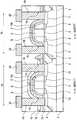
도 25는, 본 발명의 실시예 2인 반도체 장치의 개략구성을 도시하는 모식적 단면도이고,25 is a schematic sectional view showing a schematic configuration of a semiconductor device of
도 26 A, B 및 도 27은, 본 발명의 실시예 2인 반도체 장치의 제조공정 중에 있어서 모식적 단면도이다. 도 25 내지 도 27에 있어서, 대향하여 왼쪽이 n형 MISFET이고, 오른쪽이 p형 MISFET이다.26A, 26B and 27 are schematic sectional views during the manufacturing process of the semiconductor device of Example 2 of the present invention. 25 to 27, the left side is an n-type MISFET and the right side is a p-type MISFET.
도 25에 도시하는 것과 같이, 본 실시예 2의 반도체 장치는, 앞에서 서술한 실시예 1에 있어서 에칭 스토퍼로서 사용된 절연막(13)을 제거한 구성으로 되어 있다.As shown in FIG. 25, the semiconductor device of the second embodiment has a configuration in which the insulating
앞에서 서술한 실시예 1과 같이 절연막(13)을 남긴 경우(도 18 참조), 게이트전극(6), 사이드 월 스페이서(9) 및 절연막9130에 따른 단차부(35a)의 최하부에 질화실리콘막(14a, 14b)의 응력이 집중하기 때문에, 질화실리콘막(14a, 14b)의 응력 기점이 사이드 월 스페이서(9)의 측벽에 잔존하는 절연막(13)에 의해 MISFET의 채널형성영역에서 떨어져 버리고, 질화실리콘막(14a, 14b)의 막응력에 의해 채널형성영역에 응력을 발생시키는 효과가 감소해버린다. 따라서,, 절연막(13)은 가능한 한 제거하는 것이 바람직하다.In the case where the insulating
단, 실시예 1과 같이 질화실리콘막(14b)보다도 앞서 질화실리콘막(14a)을 형성하는 경우에는, p형 MISFET상의 질화실리콘막(14a)을 제거하는 공정에 있어서 절연막(13)이 필요하고, 실시예 1의 변형예와 같이 질화실리콘막(14a)보다도 먼저 질화실리콘막(14b)을 형성하는 경우에는, n형 MISFET상의 질화실리콘막(14b)을 제거하는 공정에 있어서 절연막(13)이 필요하므로, 이들의 공정을 고려하여 절연막(13)을 제거한다.However, when forming the
질화실리콘막(14b)보다도 먼저 질화실리콘막(14a)을 형성하는 경우, n형 MISFET상의 절연막(13)의 제거는, 도 26A에 도시하는 것과 같이, 질화실리콘막(14a)을 형성하는 공정 전에 행하고, p형 MISFET상의 절연막(13)의 제거는, 도 13에 대응하는 도 26B 및 도 27에 도시하는 것과 같이, p형 MISFET상의 질화실리콘막(14a)을 제거한 후에 행한다. 즉, 도 26B 및 도 27에 도시하는 것과 같이, p형 MISFET상의 절연막(15) 및 질화실리콘막(14a)을 제거한 후에, p형 MISFET상의 절연막(13)을 제거한다.In the case where the
질화실리콘막(14a)보다도 먼저 질화실리콘막(14b)을 형성하는 경우, p형 MISFET상의 절연막(13) 제거는, 질화실리콘막(14b)을 형성하는 공정 전에 행하고, n형 MISFET상의 절연막(13) 제거는, n형 MISFET상의 질화실리콘막(14b)을 제거한 후에 행한다. n형 MISFET상의 절연막(13)의 제거는, p형 MISFET상을 예를 들면 포토레지스트 마스크 등으로 덮은 상태에서 행하고, p형 MISFET상의 절연막(13) 게저는, n형 MISFET상을 예를 들면 포토레지스트 마스크 등으로 덮은 상태에서 행한다.In the case where the
n형 MISFET상, 혹은 p형 MISFET상의 절연막(13) 제거는, 단차부에 에칭잔여 물이 발생하지 않는 등방성 드라이 에칭으로 행하는 것이 바람직하다. 산화실리콘막으로 이루어지는 절연막(13)의 등방성 드라이 에칭으로서는, 일반적으로, CF4에 H2가스를 혼합한 가스, 혹은 CF3가스를 이용한 등방성 플라즈마 에칭이 사용되고 있다. 이 등방성 플라즈마 에칭에서는, 실리콘과 실리사이드층에 대해 충분히 선택비를 취할 수 있기 때문에, p형 기판(1), 실리사이드층(12), 및 사이드 월 스페이서(9) 등이 크게 깎여버리는 일은 없다.The removal of the insulating
또한, 본 실시예 2에서는, n형 MISFET상 및 p형 MISFET상의 양쪽 절연막(13)을 제거하는 예에 관해 설명했지만, 어느 한쪽의 절연막(13)을 남기도록 해도 좋다.In addition, in Example 2, although the example in which the both insulating
(실시예 3)(Example 3)
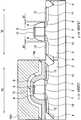
도 28은, 본 발명의 실시예 3인 반도체 자이의 제조공정 중에 있어서, 모식적 단면도이다. 도 28에 있어서, 대향하여 왼쪽이 n형 MISFET이고, 오른쪽이 p형 MISFET이다.28 is a schematic cross sectional view of the semiconductor device according to a third embodiment of the present invention. In Fig. 28, the left side is an n-type MISFET and the right side is a p-type MISFET.
앞에서 서술한 실시예 1에서는, 퇴적법으로 형성된 산화실리콘막으로 이루어지는 절연막(13)을 질화실리콘막(14a)의 가공시의 에칭 스토퍼로서 이용한 예에 관해 설명했지만, 본 실시예 3에서는, 열산화법으로 형성된 산화실리콘막으로 이루어지는 절연막(21)을 질화실리콘막(14a)의 가공시 에칭 스토퍼로서 이용하고 있다. 열산화법에 의한 절연막(21)의 형성은, 살리사이드구조의 n형 및 p형 MISFET을 형성하는 공정의 다음이고, 질화실리콘막(14a) 및 (14b)를 형성하는 공정 앞에 행한 다.In Example 1 mentioned above, the example which used the insulating
열산화법에서는, 도 28에 도시하는 것과 같이 게이트전극(6)의 표면 실리사이드층(12)상, 및 반도체 영역(10, 11)의 표면 실리사이드층(12)상에 이들의 실리사이드층(12)을 덮도록 하여 절연막(21)을 선택적으로 형성할 수 있다. 따라서, 앞에서 서술한 실시예 1과 같이 질화실리콘막(14b)보다도 먼저 질화실리콘막(14a)을 형성하는 경우와, 앞에서 서술한 실시예 1의 변형예와 같이 질화실리콘막(14a)보다도 먼저 질화실리콘막(14b)을 형성하는 경우에 있어서도, 질화실리콘막(14a, 14b)을 등방성 드라이 에칭으로 가공할 때에 발생하는 불합리함을 절연막(21)으로 억제할 수 있다.In the thermal oxidation method, as shown in FIG. 28, the
(실시예 4)(Example 4)
도 29는, 본 발명의 실시예 4인 반도체 장치의 제조공정 중에 있어서 모식적 단면도이다. 도 29에 있어서, 대향하여 왼쪽이 n형 MISFET이고, 오른쪽이 p형 MISFET이다.29 is a schematic cross sectional view of the semiconductor device of Example 4 of the present invention during a manufacturing step; In Fig. 29, the left side is an n-type MISFET and the right side is a p-type MISFET.
앞에서 서술한 실시예 1에서는, 퇴적법으로 형성된 산화실리콘막으로 이루어지는 절연막(13)을 질화실리콘막(14a)의 가공시의 에칭 스토퍼로 이용한 예에 관해 설명했지만, 본 실시예 4에서는 사이드 월 스페이서(9)의 측벽에 형성된 산화실리콘막으로 이루어지는 사이드 월 스페이서(22)를 질화실리콘막(14a)의 가공시의 에칭 스토퍼로서 이용하고 있다. 사이드 월 스페이서(22)의 형성은, 살리사이드구조의 n형 및 p형 MISFET을 형성하는 공정 다음이고, 질화실리콘막(14a) 및 (14b)을 형성하는 공정 앞에 행한다. 사이드 월 스페이서(22)는 사이드 월 스페이서(9)와 동일한 방법으로 형성된다.In Example 1 mentioned above, the example which used the insulating
이렇게 사이드 월 스페이서(9)의 측벽에 산화실리콘막으로 이루어지는 사이드 월 스페이서(22)를 형성하므로써, 반도체 영역(10, 11)의 표면에 있어서 실리사이드층(12)의 사이드 월 스페이서(9)측 단부, 및 사이드 월 스페이서(9)를 사이드 월 스페이서(22)로 덮을 수 있으므로, 앞에서 서술한 실시예 1과 같이, 질화실리콘막(14b)보다도 먼저 질화실리콘막(14a)을 형성하는 경우와, 앞에서 서술한 실시예 1의 변형예와 같이, 질화실리콘막(14a)보다도 먼저 질화실리콘막(14b)을 형성하는 경우에 있어서도, 질화실리콘막(14a, 14b)을 등방성 드라이 에칭으로 가공할 때에 발생하는 불합리, 특히 사리드 월 스페이서(9)의 후퇴에 관한 불합리를 사이드 월 스페이서(22)로 억제할 수 있다.By forming the
또한, 본 실시예 4에서는, 산화실리콘막으로 이루어지는 사이드 월 스페이서(22)를 질화실리콘막(14a, 14b)의 가공시 에칭 스토퍼로서 이용한 예에 관해 설명했지만, 이에 한정되는 것은 아니고, 질화실리콘막(14a, 14b)의 가공시의 등방성 드라이 에칭에 대해 선택비를 취할 수 있는 것이면 다른 절연막을 이용해도 좋다.In addition, in Example 4, although the example which used the
(실시예 5)(Example 5)
도 30A, B는, 본 발명의 실시예 5인 반도체 장치의 개략구성을 도시하는 모식적 단면도이다. 도 30A, B에 있어서, 대향하여 왼쪽이 n형 MISFET이고, 오른쪽이 p형 MISFET이다.30A and 30B are schematic cross sectional views showing a schematic configuration of a semiconductor device according to a fifth embodiment of the present invention. 30A and B, the left side is an n-type MISFET and the right side is a p-type MISFET.
앞에서 서술한 실시예 1에서는, 살리사이드구조의 상보형 MISFET을 갖는 반 도체 장치에 본 발명을 적용한 예에 관해 설명했지만, 본 실시예 5에서는, 실리사이드층을 갖지 않는 상보형 MISFET을 갖는 반도체 장치에 본 발명을 적용한 예에 관해 설명한다.In Example 1 described above, an example in which the present invention is applied to a semiconductor device having a salicide structured complementary MISFET has been described. In the fifth embodiment, a semiconductor device having a complementary MISFET having no silicide layer is used. The example which applied this invention is demonstrated.
도 30A에 도시하는 것과 같이, 본 실시예 5의 반도체 장치는, 기본적으로 앞에서 서술한 실시예 1과 동일한 구성으로 되어 있고, n형 및 p형 MISFET의 구조가 다르다. 즉, 본 실시예 5의 n형 및 p형 MISFET은, 게이트전극(6)의 표면, 및 반도체 영역(10, 11)의 표면에 실리사이드층을 갖지 않는 구조로 되어 있다.As shown in Fig. 30A, the semiconductor device of the fifth embodiment is basically the same as that of the first embodiment described above, and the structures of the n-type and p-type MISFETs are different. In other words, the n-type and p-type MISFETs of the fifth embodiment have a structure in which no silicide layer is provided on the surface of the
본 실시예 5의 반도체 장치는, 실리사이드층을 형성하는 공정을 제외하고 앞에서 서술한 실시예 1에서 설명한 방법으로 형성되어 있다.The semiconductor device of the fifth embodiment is formed by the method described in the first embodiment described above except for the step of forming the silicide layer.
p형 MISFET상의 질화실리콘막(14a)을 등방성 드라이 에칭으로 제거할 때, 실시예 1과 같이 p형 MISFET이 살리사이드구조인 경우는, 실리사이드층(12)이 에칭 스토퍼의 역할을 하기 때문에, 게이트전극(6)에 있어서는 실리사이드층(12)하의 다결정 실리콘막, 소스영역 및 드레인영역에 있어서는 실리사이드층(12)하의 p형 반도체 영역(11)이 질화실리콘막(14a)의 가공시 오버 에칭에 의해 깎여져버리는 일이 없지만, 본 실시예 5와 같니 p형 MISFET이 게이트전극(6)의 표면과 p형 반도체 영역(11)의 표면에 실리사이드층(12)을 갖지 않는 구조인 경우는, 도 23에 도시하는 것과 같이, 게이트전극(6)의 다결정 실리콘막, 소스영역 및 드레인영역의 p형 반도체 영역(11)이 깎여져버린다.When the
이러한 문제는, 질화실리콘막(14a)을 형성하는 공정 전에, 게이트전극(6)상, 및 p형 반도체 영역(11)상을 에칭 스토퍼로서 기능하는 절연막(13)으로 덮어두므로 써 해결할 수 있다.This problem can be solved by covering the
본 실시예 5에서는 에칭 스토퍼로서 절연막(13)을 이용하고 있다. 이 절연막(13)은 퇴적법으로 형성되어 있다. 퇴적법은, 게이트전극(6)상 및 p형 반도체 영역(11)상을 일괄적으로 절연막(13)으로 덮을 수 있기 때문에, 게이트전극(6) 및 p형 반도체 영역(11)의 깎임을 동시에 억제할 수 있다.In the fifth embodiment, the insulating
또한, 본 실시예 5에서는 질화실리콘막(14b)보다도 먼저 질화실리콘막(14a)을 형성하는 예에 관해 설명했지만, 질화실리콘막(14a)보다도 먼저 질화실리콘막(14b)을 형성하는 경우에 있어서도, 동일한 효과를 얻을 수 있다.In addition, in the fifth embodiment, the example in which the
또, 본 실시예 5에서는, 에칭 스토퍼로서 절연막(13)을 이용한 예에 관해 설명했지만, 열산화법으로 형성된 절연막(21)을 에칭 스토퍼호러 이용하는 경우에 있어서도, 동일한 효과를 얻을 수 있다. 또, 본 실시예 5에서는, 에칭 스토퍼로서 기능하는 절연막을 남기는 예에 관해 설명했지만, 도 30B에 도시하는 것과 같이, 절연막(13)은 실시예 2와 같이 제거해도 좋다.In the fifth embodiment, the example in which the insulating
또, 본 실시예 5의 실리사이드층을 갖지 않는 MISFET은, 예를 들면 앞에서 서술한 실시예 1 ~ 4의 실리사이드층을 갖는 MISFET과 동일기판상에 형서되고, 소스영역 또는 드레인영역과 기판 사이의 (접합) 리크전류를 저감하고싶은 MISFET 및 회로를 구성한다. 즉, 접합리크전류를 저감할 필요가 있는 MISFET을 본 실시예 5의 실리사이드층을 갖지 않는 MISFET으로 구성하고, 고속동작을 필요로 하는 MISFET을 실시예 1 ~ 4의 실리사이드층을 갖는 MISFET으로 형성한다. 이에 의해, 저소비전력화 및 고속동작을 도모할 수 있다.In addition, the MISFET which does not have the silicide layer of the fifth embodiment is, for example, formed on the same substrate as the MISFET having the silicide layers of the first to fourth embodiments described above, and is formed between the source region or the drain region and the substrate ( Junction) Configure MISFET and circuit to reduce leakage current. That is, the MISFET which needs to reduce the junction leakage current is constituted by the MISFET which does not have the silicide layer of the fifth embodiment, and the MISFET which requires the high speed operation is formed by the MISFET having the silicide layer of the first to fourth embodiments. . As a result, low power consumption and high speed operation can be achieved.
또, 절연막(13)은, 실리사이드층을 갖지 않는 MISFET 및 실리사이드층을 갖는 MISFET상에 동일공정으로 퇴적할 수 있으므로, 제조공정을 늘리지 않고 저소비전력 및 고속동작이 가능한 반도체 장치를 형성할 수 있다.In addition, since the insulating
또, 실리사이드층을 갖는 MISFET과 실리사이드층을 갖지 않는 MISFET을 동일기판에 형성하는 경우, 실리사이드층을 갖는 MISFET에 있어서는, 도 25에 도시하는 것과 같이 에칭 스토퍼로서 기능하는 절연막(13)을 설치하지 않는 구조로 하고, 실리사이드층을 갖지 않는 MISFET에 있어서는, 도 30A에 도시하는 것과 같이 에칭 스토퍼로서 기능하는 절연막(13)을 설치한 구조로 해도 좋다.In the case where a MISFET having a silicide layer and a MISFET having no silicide layer are formed on the same substrate, in the MISFET having a silicide layer, as shown in FIG. 25, an insulating
이 경우, 실리사이드층을 갖는 MISFET상의 절연막(13)의 제거는, 실리사이드층을 갖는 MISFET의 채널형성영역에 응력을 발생시키는 제 1 막을 먼저 형성하든지, 그렇지 않으면 실리사이드층을 갖지 않는 MISFET의 채널형성영역에 응력을 발생시키는 제 2 막을 먼저 형성하든지로 다르다. 예를 들면, 실리사이드층을 갖는 MISFET이 n형, 실리사이드층을 갖지 않는 MISFET이 p형인 경우, 제 1 막(질화실리콘막(14a))을 먼저 형성하는 경우는, 도 25(도 중 우측 p형 MISFET을 실리사이드층을 갖지 않는 p형 MISFET으로 치환하여 참조)에 도시하는 것과 같이, 질화실리콘막(14a)을 형성하는 공정 전에, 실리사이드층을 갖는 MISFET상의 절연막(13)을 선택적으로 제거하고, 제 2 막(질화실리콘막(14b))을 먼저 형성하는 경우는, 실리사이드층을 갖는 MISFET상의 질화실리콘막(14b)을 선택적으로 제거하는 공정 다음이고, 질화실리콘막(14a)을 형성하는 공정 전에, 실리사이드층을 갖는 MISFET상의 절연막(13)을 선택적으로 제거한다. 또, 실리사이드층을 갖는 MISFET이 p형, 실리사이드층을 갖지 않는 MISFET이 n형인 경우, 동일하게 하여, 실리사이드층을 갖는 MISFET상의 절연막(13)을 선택적으로 제거한다. 또한, 실리사이드층을 갖는 MISFET과 실리사이드층을 갖지 않는 MISFET을 동일기판에 형성하는 경우, 실리사이드층을 갖는 MISFET에 있어서는 도 25에 도시하는 것과 같이 실리사이드층을 갖지 않는 MISFET에 있어서는, 도 30B에 도시하는 것과 같이, 에칭 스토퍼로서 기능하는 절연막을 설치하지 않는 구조로 해도 좋다. 이 경우, 실리사이드층을 갖는 MISFET 및 실리사이드층을 갖지 않는 MISFET에 있어서, 절연막(13)을 제거하는 공정을 공통화하므로써, 실시예 2에 도시하는 절연막(13) 제거공정과 동일한 공정수로 형성할 수 있으므로, 제조공정을 저감할 수 있다.In this case, the removal of the insulating
(실시예 6)(Example 6)
도 31은, 본 발명의 실시예 6인 반도체 장치의 개략구성을 도시하는 모식적 단면도이고, 도 32 내지 도 35는, 본 발명의 실시예 6인 반도체 장치의 제조공정 중에 있엇 모식적 단면도이다. 도 31 내지 도 35에 있어서, 대향하여 왼쪽이 n형 MISFET이고, 오른쪽이 p형 MISFET이다.FIG. 31 is a schematic sectional view showing a schematic configuration of a semiconductor device according to a sixth embodiment of the present invention, and FIGS. 32 to 35 are schematic sectional views during a manufacturing process of the semiconductor device according to a sixth embodiment of the present invention. 31 to 35, the left side is an n-type MISFET and the right side is a p-type MISFET.
본 실시예 6은, n형 MISFET의 채널형성영여게 인장응력을 발생시키는 막상에, p형 MISFET의 채널형성영역에 압축응력을 발생시키는 막을 겹치고, n형 및 p형 MISFET의 드레인전류의 증가를 노린 것이다.In the sixth embodiment, a film generating compressive stress in a channel forming region of a p-type MISFET is superimposed on a film generating tensile stress for the channel formation of an n-type MISFET. It is aimed.
도 31에 도시하는 것과 같이 n형 및 p형 MISFET은, 질화실리콘막(14a)으로 덮여져 있다. 또, p형 MISFET은, 질화실리콘막(14b)으로 덮여있다. 즉, n형 MISFET상에는 질화실리콘막(14a)만이 존재하고, p형 MISFET상에는 질화실리콘막(14a) 및 (14b)이 존재하고 있다.As shown in FIG. 31, the n-type and p-type MISFETs are covered with the
n형 MISFET상에는 질화실리콘막(14a)만이 존재하고 있기 때문에, n형 MISFET의 채널형성영역에는 질화실리콘막(14a)의 인장응력만이 가해지지만, p형 MISFET상에는 질화실리콘막(14a) 및 (14b)가 존재하고 있으므로, p형 MISFET의 채널형성영역에는 질화실리콘막(14a)의 인장응력 및 질화실리콘막(14b)의 압축응력이 가해진다. 따라서, 적어도 질화실리콘막(14a)의 인장응력보다도 절대치가 큰 압축응력을 갖는 질화실리콘막(14b)을 이용하므로써, p형 MISFET의 채널형성영역에 압축응력을 발생시킬 수 있다.Since only the
또한, 본 실시예 6에서는 압축응력을 갖는 질화실리콘막(14b)이 인장응력을 갖는 질화실리콘막(14a)보다도 상층에 형성되어 있기 때문에, p형 MISFET의 채널형성영역에 대한 막응력의 기점은, 질화실리콘막(14a)보다도 질화실리콘막(14b)쪽이 멀어져 있다. 따라서, 이러한 경우에는, 질화실리콘막(14a)의 인장응력보다도 절대치가 2배 이상인 압축응력을 갖는 질화실리콘막(14b)을 이용하는 것이 바람직하다.In addition, in the sixth embodiment, since the
다음으로, 본 실시예 6의 반도체 장치의 제조에 관해, 도 32 내지 도 35를 이용하여 설명한다.Next, manufacturing of the semiconductor device of the sixth embodiment will be described with reference to FIGS. 32 to 35.
도 32에 도시하는 것과 같이, 앞에서 서술한 실시예 1과 동일한 프로세스로, 살리사이드구조의 n형 및 p형 MISFET을 형성한다.As shown in Fig. 32, n-type and p-type MISFETs having salicide structures are formed by the same process as in Example 1 described above.
다음으로, 도 33에 도시하는 것과 같이, n형 및 p형 MISFET상을 포함하는 p형 기판(1)의 회로형성면상의 전면에, 예를 들면 100 ~ 120nm 정도 두께의 질화실리콘막(14a)을 플라즈마 CVD법으로 형성한다. 질화실리콘막(14a)의 형성은, 예를 들면 고주파전력 350 ~ 400W의 조건으로 행한다.Next, as shown in FIG. 33, a
다음으로, 도 34에 도시하는 것과 같이, n형 및 p형 MISFET상을 포함하는 p형 기판(1)상의 전면에, 예를 들면 50nm 정도 두께의 산화실리콘막으로 이루어지는 절연막(15)을 CVD법으로 형성하고, 그 후, n형 및 p형 MISFET상을 포함하는 p형 기판(1)상의 전면에, 예를 들면 100 ~ 200nm 정도 두께의 질화실리콘막(14b)을 플라즈마 CVD법으로 형성한다. 질화실리콘막(14b)의 형성은, 예를 들면 고주파전력 600 ~ 700W의 조건으로 행한다.Next, as shown in FIG. 34, an insulating
이 공정에 있어서, 최종적으로 p형 MISFET의 채널형성영역에 압축응력이 발생하도록 적어도 질화실리콘막(14a)의 인장응력보다도 절대치가 큰 압축응력을 갖는 질화실리콘막(14b)을 형성한다. 본 실시예에서는, 질화실리콘막(14a)의 인장응력보다도 절대치가 2배 이상의 압축응력을 갖도록 질화실리콘막(14b)을 형성했다.In this step, a
다음으로, 질화실리콘막(14b)상에, p형 MISFET상을 선택적으로 덮는 포토레지스트 마스크(RM3)을 형성하고, 그 후, 포토레지스트 마스크(RM3)을 에칭 마스크로 하여 에칭처리를 실시하고, 도 35에 도시하는 것과 같이 n형 MISFET상의 질화실리콘막(14b)을 제거한다. 질화실리콘막(14b)의 가공은 등방성 드라이 에칭으로 행한다.Next, a photoresist mask RM3 is formed on the
이 후, 포토레지스트 마스크(RM3)을 제거하므로써, 도 31에 도시하는 상태가 된다.Thereafter, the photoresist mask RM3 is removed to enter the state shown in FIG. 31.
이렇게, n형 및 p형 MISFET상에 질화실리콘막(14a)을 형성하고, 그 후, p형 MISFET상에 질화실리콘막(14a)의 인장응력보다도 절대치가 큰 압축응력을 갖는 질 화실리콘막(14b)을 선택적으로 형성하므로써, p형 MISFET의 채널형성영역에 압축응력을 발생시킬 수 있기 때문에, 본 실시예에 있어서도, n형 MISFET 및 p형 MISFET의 드레인전류를 동시에 증가시킬 수 있다.Thus, a
또, 본 실시예 6에서는, p형 MISFET상의 질화실리콘막(14a)의 제거를 하고 있지 않으므로, 앞에서 서술한 실시예 1과 같이 에칭 스토퍼로서 기능하는 절연막(13)을 형성할 필요가 없다. 따라서, 앞에서 서술한 실시예 1과 비교하여 제조공정수를 간략화할 수 있다.In the sixth embodiment, since the
또한, 본 실시예 6에서는, n형 및 p형 MISFET상을 덮는 질화실리콘막(14a) 다음에, p형 MISFET상만을 덮는 질화실리콘막(14b)을 형성한 예에 관해 설명했지만, p형 MISFET상을 덮는 질화실리콘막(14a) 앞에 형성해도 좋다. 단, 이 경우는, 앞에서 서술한 실시예 1과 같이, 질화실리콘막(14b)의 가공시에 에칭 스토퍼로서 기능하는 절연막이 필요하다.In the sixth embodiment, the
도 36은, 본 발명의 실시예 6의 변형예인 반도체 장치의 개략구성을 도시하는 모식적 단면도이다. 도 36에 있어서, 대향하여 왼쪽이 n형 MISFET이고, 오른쪽이 p형 MISFET이다.36 is a schematic sectional view showing a schematic configuration of a semiconductor device of Modification Example 6 of the present invention. In Fig. 36, the left side is an n-type MISFET and the right side is a p-type MISFET.
앞에서 서술한 실시예 6에서는 n형 및 p형 MISFET상에 인장응력을 갖는 질화실리콘막(14a)을 형성하고, 또한, p형 MISFET상에 질화실리콘막(14a)의 인장응력보다도 절대치가 큰 압축응력을 갖는 질화실리콘막(14b)을 선택적으로 형성하고, n형 및 p형 MISFET의 드레인전류를 동시에 증가시킨 예에 관해 설명했지만, 도 36에 도시하는 것과 같이 n형 및 p형 MISFET상에 압축응력을 갖는 질화실리콘막(14b)을 형 성하고, 또한, n형 MISFET상에 질화실리콘막(14b)의 압축응력보다도 절대치가 큰 인장응력을 갖는 질화실리콘막(14a)을 선택적으로 형성해도 좋다. 이러한 경우에 있어서도, n형 MISFET 및 p형 MISFET의 드레인전류를 동시에 증가시킬 수 있다.In Example 6 described above, a
또한, 도 36에서는 n형 및 p형 MISFET상을 덮는 질화실리콘막(14b) 다음에, n형 MISFET상만을 덮는 질화실리콘막(14a)을 형성한 예에 관해 도시하고 있지만, n형 MISFET상만을 덮는 질화실리콘막(14a)는, n형 및 p형 MISFET상을 덮는 질화실리콘막(14b) 앞에 형성해도 좋다. 단, 이 경우는, 앞에서 서술한 실시예 1과 같이 질화실리콘막(14b)의 가공시에 에칭 스토퍼로서 기능하는 절연막이 필요해진다. 36 shows an example in which the
(실시예 7)(Example 7)
도 37은, 본 발명의 실시예 7인 반도체 장치의 개략구성을 도시하는 모식적 단면도이고, 도 38 및 도 39는, 본 발명의 실시예 7인 반도체 장치의 제조공정 중에 있어서 모식적 단면도이다. 도 37 내지 도 39에 있어서, 대향하여 왼쪽이 n형 MISFET이고, 오른쪽이 p형 MISFET이다.37 is a schematic sectional view showing a schematic configuration of a semiconductor device according to a seventh embodiment of the present invention, and FIGS. 38 and 39 are schematic sectional views during a manufacturing process of the semiconductor device according to a seventh embodiment of the present invention. 37 to 39, the left side is an n-type MISFET and the right side is a p-type MISFET.
본 실시예 7은, 하나의 질화실리콘막이고, n형 및 p형 MISFET의 드레인전류의 증가를 노린 것이다.In the seventh embodiment, one silicon nitride film is intended to increase the drain current of n-type and p-type MISFETs.
도 37에 도시하는 것과 같이 n형 및 p형 MISFET은, 하나의 질화실리콘막(24)로 덮여져 있다. 질화실리콘막(24)은, n형 MISFET의 채널형성영역에 인장응력을 발생시키는 제 1 부분(24a)과, p형 MISFET의 채널형성영역에 압축응력을 발생시키는 제 2 부분(24b)을 갖고, 제 1 부분(24a)은 n형 MISFET상에 그 게이트전극(6)을 덮도록 하여 형성되고, 제 2 부분(24b)은 p형 MISFET상에 그 게이트전극(6)을 덮도록 하여 형성되어 있다. 제 2 부분(24b)은, Si 및 N의 원소농도가 제 1 부분(24a)보다도 높아져 있다. 이하, 본 실시예 7의 반도체 장치의 제조에 관해, 도 38 및 도 37을 이용하여 설명한다.As shown in FIG. 37, the n-type and p-type MISFETs are covered with one
앞에서 서술한 실시예 1과 동일한 프로세스에서, 살리사이드구조의 N형 및 p형 MISFET을 형성한 후, 도 38에 도시하는 것과 같이 n형 및 p형 MISFET상을 포함하는 p형 기판(1)의 회로형성면상의 전면에, n형 MISFET의 채널형성영역에 인장응력을 발생시키는 질화실리콘막(24)을 플라즈마 CVD법으로 형성한다. 질화실리콘막(24)의 형성은, 예를 들면 고주파전력 350 ~ 400W의 조건으로 행한다.In the same process as in Example 1 described above, after the N-type and p-type MISFETs having a salicide structure are formed, the p-
다음으로, n형 MISFET상을 덮고, 또한 p형 MISFET상에 개구를 갖는 포토레지스트 마스크(RM4)를 질화실리콘막(24)상에 형성하고, 그 후, 도 39에 도시하는 것과 같이 포토레지스트 마스크(RM4)를 마스크로 하여, 포토레지스트 마스크(RM4)에서 노출하는 질화실리콘막(24) 중(p형 MISFET상의 질화실리콘막(24) 중)에, Si 및 n의 운소를 이온투입법으로 도입한다. 이온투입은, 막의 깊이방향 전반에 걸쳐 이들의 원소가 도입되도록 깊이방향에 있어서 원소농도의 피크치(Rp)가 막두께의 1/2 정고가 되는 가속에너지, 도즈량이 1 ×10¹⁵/cm2이상의 조건으로 행한다.Next, a photoresist mask RM4 covering the n-type MISFET and having an opening on the p-type MISFET is formed on the
이 공정에 있어서, 제 1 부분(24a)과, 이 제 1 부분(24a)보다도 원소농도가 높은 제 2 부분(24b)을 갖는 질화실리콘막(24)이 형성된다.In this step, a
다음으로, 포토레지스트 마스크(RM4)를 제거한 후, 열처리를 실시하여 질화실리콘막(24)의 제 2 부분(24b)을 활성화한다.Next, after removing the photoresist mask RM4, heat treatment is performed to activate the
이 공정에 있어서, 질화실리콘막(24)의 제 2 부분(24b)이 체적팽창하고, 제 2 부분(24b)이 p형 MISFET의 채널형성영역에 압축응력을 발생시키는 막으로 변환한다. 따라서, 도 37에 도시하는 것과 같이 질화실리콘막(24)은, n형 MISFET의 채널형성영역에 인장응력을 발생시키는 제 1 부분(24a)과, p형 MISFET의 채널형성영역에 압축응력을 발생시키는 제 2 부분(24b)를 갖는 구성이 된다.In this step, the
이렇게 해서 질화실리콘막(24)을 형성하므로써, 본 실시예 7에 있어서도 n형 MISFET 및 p형 MISFET의 드레인전류를 동시에 증가시킬 수 있다.By forming the
또, 본 실시예 7에서는 p형 MISFET상의 질화실리콘막(24)의 제거를 하고 있지 않기 때문에, 앞에서 서술한 실시예 1과 같이 에칭 스토퍼로서 기능하는 절연막(13)을 형성할 필요가 없다. 따라서, 앞에서 서술한 실시예 1과 비교하여 제조공정수를 간략화할 수 있다.In the seventh embodiment, since the
또, 본 실시예 7에서는 n형 및 p형 MISFET의 드레인전류가 증가하도록 하나의 질화실리콘막(24)으로 억제할 수 있기 때문에, 앞에서 서술한 실시예 1과 비교하여 질화실리콘막의 피막공정이 1회로 끝난다. 따라서, 질화실리콘막의 피막공정과 그 가공공정을 생략할 수 있고, 제조공정을 간략화할 수 있다.In addition, in the seventh embodiment, since the
도 40은, 본 발명의 실시예 7의 변형예인 반도체 장치의 제조공정 중에 있어서 모식적 단면도이다.40 is a schematic cross sectional view of the semiconductor device during a manufacturing step of Modification Example 7 of the present invention.
앞에서 서술한 실시예 7에서는 Si 및 N의 원소를 도입하는 방법으로, p형 기판(1)에 대해 수직으로 원소를 이온투입하는 방법을 적용한 경우를 도시했지만, 도 40에 도시하는 것과같이 p형 기판(1)에 대해 비스듬하게 원소를 이온주입하는 방법 을 적용해도 좋다. 이 경우, 사이드 월 스페이서(9)의 측벽을 덮고 있는 질화실리콘막(24)의 게이트측벽부분(단차부분)에도 원소를 도입할 수 있다. 이 결과, 한층 더 좋은 압축응력 발생효과를 얻을 수 있다.In Example 7 described above, a method in which the element is ion-implanted with respect to the p-
(실시예 8)(Example 8)
도 41은, 본 발명의 실시예 8인 반도체 장치의 개략구성을 도시하는 모식적 단면도이다.41 is a schematic sectional view showing a schematic configuration of a semiconductor device of
본 실시예 8은, 세로형 더블 게이트구조의 상보형 MISFET을 갖는 반도체 장치에 본 발명을 적용한 예이다.In the eighth embodiment, the present invention is applied to a semiconductor device having a complementary MISFET having a vertical double gate structure.
도 41에 도시하는 것과 같이, 본 실시예 8의 반도체 장치는, SOI(Silicon On Insulator)구조의 반도체 기판(이하, 간단히 기판이라 한다.)(40)을 주체로 구성되어 있다. 기판(40)은, 예를 들면, 반도체층(40a)과, 이 반도체층(40a)상에 설치된 절연층(40b)과, 이 절연층(40b)상에 설치된 반도체층(40a)상에 설치된 절연층(40b)과, 이 절연층(40b)상에 설치된 반도체층(40c)을 갖는 구성으로 되어있다. 반도체층(40a) 및 (40c)는 예를 들면 단결정실리콘으로 이루어지고, 절연층(40b)은 예를 들면 산화실리콘으로 이루어진다.As shown in Fig. 41, the semiconductor device of the eighth embodiment is mainly composed of a semiconductor substrate (hereinafter simply referred to as a substrate) 40 having an SOI (Silicon On Insulator) structure. The
반도체층(40c)은, 복수의 소자형성부로 분할되고, 각 소자형성부에 n형 MISFET, 혹은 p형 MISFET이 형성되어 있다. n형 MISFET이 형성되는 반도체층(40c)에는 p형 웰영역(2)이 설치되고, p형 MISFET이 형성되는 반도체층(40c)에는 n형 웰영역(3)이 설치되어 있다. 각 반도체층(40c)은, 절연층(40b)상에 설치된 절연막(41)으로 주위를 둘러싸고, 서로 절연분리되어 있다.The
본 실시예 8의 n형 및 p형 MISFET은, 채널형성영역으로 사용되는 반도체층(40c)을 기판(40)의 평면방향(표면방향)으로 두개의 게이트전극(6)으로 끼워넣은 더블 게이트구조로 되어있다. 또, n형 및 p형 MISFET은, 드레인전류가 기판(40)의 두께방향으로 흐르는 세로형 구조로 되어있다.The n-type and p-type MISFETs of the eighth embodiment have a double gate structure in which a
n형 MISFET의 채널형성영역에 인장응력을 발생시키는 질화실리콘막(14a)은, n형 MISFET상에 그 두개의 게이트전극(6)을 덮도록 하여 형성되고, p형 MISFET의 채널형성영역에 압축응력을 발생시키는 질화실리콘막(14b)은, p형 MISFET상에 그 두개의 게이트전극(6)을 덮도록 하여 형성되어 있다.The
본 실시예 8에 있어서, n형 및 p형 MISFET은, 채널형성영역으로서 사용되는 반도체층(40c)을 기판(40)의 평면방향에서 두개의 게이트전극(6)으로 끼워넣은 더블 게이트구조로 되어 있기 때문에, 질화실리콘막에 의한 응력의 영향이 배증하고, 드레인전류 증가비율도 실글게이트구조의 종래형보다 증가한다.In the eighth embodiment, the n-type and p-type MISFETs have a double gate structure in which a
(실시예 9)(Example 9)
도 42는, 본 발명의 실시예 9인 반도체 장치의 개략구성을 도시하는 모식적 평면도이고, 도 43은, 도 42의 A-A선을 따른 모식적 단면도이다.FIG. 42 is a schematic plan view showing a schematic configuration of a semiconductor device according to a ninth embodiment of the present invention, and FIG. 43 is a schematic sectional view along the line A-A in FIG. 42.
본 실시예 9는, 가로형 더블 게이트구조의 상보형 MISFET을 갖는 반도체 장치에 본 발명을 적용한 예이다.In the ninth embodiment, the present invention is applied to a semiconductor device having a complementary MISFET having a horizontal double gate structure.
도 42 및 도 43에 도시하는 것과 같이, 본 실시예 9의 n형 및 p형 MISFET은 채널형성영역으로 사용되는 반도체층(40c)을 기판(40)의 평면방향에서 두개의 게이트전극(6)으로 끼워넣은 더블 게이트구조로 되어있다. 또, n형 및 p형 MISFET은, 드레인전류가 반도체 기판(40)의 평면방향으로 흐르는 가로형 구조로 되어있다.As shown in Figs. 42 and 43, the n-type and p-type MISFETs of the ninth embodiment use a
n형 MISFET의 채널형성영역에 인장응력을 발생시키는 질화실리콘막(14a)은, n형 MISFET상에 그 두개의 게이트전극(6)을 덮도록 하여 형성되고, p형 MISFET의 채널형성영역에 압축응력을 발생시키는 질화실리콘막(14b)은, p형 MISFET상에 그 두개의 게이트전극(6)을 덮도록 하여 형성되어 있다.The
본 실시예 9에 있어서, n형 및 p형 MISFFET은, 채널형성영역으로 하여 사용되는 반도체층(40c)을 기판(40)의 평면방향에서 두개의 게이트전극(6)으로 끼워넣은 더블 게이트구조로 되어있기 때문에, 질화실리콘막에 의한 응력의 영향이 배증하고, 드레인전류증가 비율도 싱글 게이트구조의 종래형보다 증가한다.In the ninth embodiment, the n-type and p-type MISFFETs have a double gate structure in which a
(실시예 10)(Example 10)
도 44는, 본 발명의 실시예 10인 반도체 장치의 개략구성을 도시하는 모식적 단면도이다.44 is a schematic sectional view showing a schematic configuration of a semiconductor device of
본 실시예 10은, 가로형 더블 게이트구조의 상보형 MISFET을 갖는 반도체 장치의 본 발명을 적용한 예이다.In the tenth embodiment, the present invention is applied to a semiconductor device having a complementary MISFET having a horizontal double gate structure.
도 44에 도시하는 것과 같이, 본 실시예 10의 반도체 장치는, 예를 들며 p형 기판(1) 주체로 구성되어있다. p형 기판(1)의 주면상에는 반도체층(42)이 설치되어 있다. 반도체층(42)은, 복수의 소자형성부로 분할되고, 각 소자형성부에 n형 MISFET, 혹은 p형 MISFET이 형성되어 있다. n형 MISFET이 형성되는 반도체층(42)에는 p형 웰영역(2)이 설치되고, p형 MISFET이 형성되는 반도체층(42)에는 n형 웰영역(3)이 설치되어 있다. 각 반도체층(42)는 p형 기판(1)상에 설치된 절연막(41)으 로 주위를 둘러싸고, 서로 절연분리되어 있다.As shown in FIG. 44, the semiconductor device of Example 10 is comprised mainly from the p-type board |
본 실시예 10의 n형 및 p형 MISFET은, 채널형성영역으로 사용되는 반도체층(42)을 p형 기판(1)의 두께방향으로 두개의 게이트전극(6)으로 끼워넣은 더블 게이트구조로 되어 있다. 또, n형 및 p형 MISFET은, 드레인전류가 기판(40)의 평면방향으로 흐르는 가로형 구조로 되어있다.The n-type and p-type MISFETs of the tenth embodiment have a double gate structure in which a
n형 MISFET은, 그 채널형성영역에 인장응력을 발생시키는 두개의 질화실리콘막(14a)에서 p형 기판(1)의 두께방향으로 끼워넣어져 있다. 한쪽 질화실리콘막(14a)은, p형 기판(1)과 n형 MISFET 사이에 설치되고, 다른 쪽 질화실리콘막(14a)은, n형 MISFET상을 덮도록 하여 설치되어 있다.The n-type MISFET is sandwiched in the thickness direction of the p-
p형 MISFET은, 그 채널형성영역에 압축응력을 발생시키는 두개의 질화실리콘막(14b)에서 p형 기판(1)의 두께방향으로 끼워넣어져 있다. 한쪽 질화실리콘막(14b)은 p형 기판(1)과 p형 MISFET 사이에 설치되고, 다른 쪽 질화실리콘막(14b)은, p형 기판(1)과 p형 MISFET 사이에 설치되고, 다른 쪽 질화실리콘막(14b)은 p형 MISFET상을 덮도록 하여 설치되어 있다.The p-type MISFET is sandwiched in the thickness direction of the p-
본 실시예 10에 있어서, n형 및 p형 MISFET은, 채널형성영역으로 사용되는 반도체층(40c)을 기판(40)의 깊이방향에서 두개의 게이트전극(6)으로 끼워넣은 더블 게이트구조로 되어 있고, 또한 두개의 질화실리콘막으로 덮여있기 때문에, 질화실리콘막에 의한 응력의 영향이 배증하고, 드레인전류 증가비율도 싱글 게이트구조의 종래형보다 증가한다.In the tenth embodiment, the n-type and p-type MISFETs have a double gate structure in which a
이상, 본 발명자에 의해 이루어진 발명을, 상기 실시예에 기초하여 구체적으 로 설명했지만, 본 발명은, 상기 실시예에 한정되는 것은 아니고, 그 요지를 일탈하지 않는 범위에 있어서 여러가지 변경가능한 것은 물론이다.As mentioned above, although the invention made by this inventor was demonstrated concretely based on the said Example, this invention is not limited to the said Example, Of course, various changes are possible in the range which does not deviate from the summary. .
예를 들면, SRAM(Static Random Access Memory), DRAM(Dynamic Random Access Memory), 플래시 메모리 등의 메모리시스템을 포함하는 제품에 있어서, 적어도 그 메모리시스템의 주변회로와 로직회로에 본 발명구조를 적용하면 보다 고성능의 메모리제품을 얻을 수 있다.For example, in a product including a memory system such as a static random access memory (SRAM), a dynamic random access memory (DRAM), a flash memory, etc., at least the present invention may be applied to peripheral circuits and logic circuits of the memory system. Higher performance memory products can be obtained.
본원에 있어서, 개시되는 발명 중 대표적인 것에 의해 얻을 수 있는 효과를 간단하게 설명하면, 하기와 같다.In this application, the effect obtained by the typical thing of the invention disclosed is demonstrated briefly as follows.
본 발명에 따르면, n채널 도전형 전계효과 트랜지스터 및 p채널 도전형 전계효과 트랜지스터의 드레인전류의 증가(전류구동능력의 향상)를 도모할 수 있게된다.According to the present invention, it is possible to increase the drain current (improve the current driving capability) of the n-channel conductivity type field effect transistor and the p-channel conductivity type field effect transistor.
또, 본 발명에 따르면, n채널도전형 전계효과 트랜지스터 및 p채널 도전형 전계효과 트랜지스터의 드레인전류비를 자유롭게 설정할 수 있게 된다.According to the present invention, the drain current ratio of the n-channel conductive field effect transistor and the p-channel conductive field effect transistor can be freely set.
Claims (45)
Translated fromKoreanApplications Claiming Priority (2)
| Application Number | Priority Date | Filing Date | Title |
|---|---|---|---|
| JP2002076182AJP4173672B2 (en) | 2002-03-19 | 2002-03-19 | Semiconductor device and manufacturing method thereof |
| JPJP-P-2002-00076182 | 2002-03-19 |
Publications (2)
| Publication Number | Publication Date |
|---|---|
| KR20030076354A KR20030076354A (en) | 2003-09-26 |
| KR101025249B1true KR101025249B1 (en) | 2011-03-29 |
Family
ID=28035421
Family Applications (1)
| Application Number | Title | Priority Date | Filing Date |
|---|---|---|---|
| KR1020030016974AExpired - Fee RelatedKR101025249B1 (en) | 2002-03-19 | 2003-03-19 | Semiconductor device and manufacturing method thereof |
Country Status (5)
| Country | Link |
|---|---|
| US (1) | US7105394B2 (en) |
| JP (1) | JP4173672B2 (en) |
| KR (1) | KR101025249B1 (en) |
| CN (1) | CN100362648C (en) |
| TW (1) | TWI272680B (en) |
Families Citing this family (257)
| Publication number | Priority date | Publication date | Assignee | Title |
|---|---|---|---|---|
| JP2000183346A (en)* | 1998-12-15 | 2000-06-30 | Toshiba Corp | Semiconductor device and manufacturing method thereof |
| JP3975099B2 (en)* | 2002-03-26 | 2007-09-12 | 富士通株式会社 | Manufacturing method of semiconductor device |
| US7388259B2 (en) | 2002-11-25 | 2008-06-17 | International Business Machines Corporation | Strained finFET CMOS device structures |
| AU2002368388A1 (en)* | 2002-11-25 | 2004-06-18 | International Business Machines Corporation | Strained finfet cmos device structures |
| US7279746B2 (en) | 2003-06-30 | 2007-10-09 | International Business Machines Corporation | High performance CMOS device structures and method of manufacture |
| JP4002219B2 (en)* | 2003-07-16 | 2007-10-31 | 株式会社ルネサステクノロジ | Semiconductor device and manufacturing method of semiconductor device |
| US20050156208A1 (en)* | 2003-09-30 | 2005-07-21 | Taiwan Semiconductor Manufacturing Company, Ltd. | Device having multiple silicide types and a method for its fabrication |
| US6949443B2 (en)* | 2003-10-10 | 2005-09-27 | Taiwan Semiconductor Manufacturing Company | High performance semiconductor devices fabricated with strain-induced processes and methods for making same |
| US7303949B2 (en) | 2003-10-20 | 2007-12-04 | International Business Machines Corporation | High performance stress-enhanced MOSFETs using Si:C and SiGe epitaxial source/drain and method of manufacture |
| US8008724B2 (en)* | 2003-10-30 | 2011-08-30 | International Business Machines Corporation | Structure and method to enhance both nFET and pFET performance using different kinds of stressed layers |
| US7015082B2 (en)* | 2003-11-06 | 2006-03-21 | International Business Machines Corporation | High mobility CMOS circuits |
| JP4653949B2 (en)* | 2003-12-10 | 2011-03-16 | ルネサスエレクトロニクス株式会社 | Semiconductor device manufacturing method and semiconductor device |
| JP4441488B2 (en)* | 2003-12-25 | 2010-03-31 | 富士通マイクロエレクトロニクス株式会社 | Semiconductor device and semiconductor integrated circuit device |
| KR100514166B1 (en)* | 2004-01-20 | 2005-09-13 | 삼성전자주식회사 | Method of forming cmos |
| JP2005294791A (en)* | 2004-03-09 | 2005-10-20 | Nec Corp | Nonvolatile memory and method of manufacturing nonvolatile memory |
| US20050214998A1 (en)* | 2004-03-26 | 2005-09-29 | Taiwan Semiconductor Manufacturing Co., Ltd. | Local stress control for CMOS performance enhancement |
| JP2005286341A (en)* | 2004-03-30 | 2005-10-13 | Samsung Electronics Co Ltd | Low noise and high performance LSI device, layout and manufacturing method thereof |
| KR101025761B1 (en)* | 2004-03-30 | 2011-04-04 | 삼성전자주식회사 | Semiconductor integrated circuit having digital circuit and analog circuit and manufacturing method thereof |
| US7101765B2 (en)* | 2004-03-31 | 2006-09-05 | Intel Corporation | Enhancing strained device performance by use of multi narrow section layout |
| US7053400B2 (en)* | 2004-05-05 | 2006-05-30 | Advanced Micro Devices, Inc. | Semiconductor device based on Si-Ge with high stress liner for enhanced channel carrier mobility |
| US7321155B2 (en)* | 2004-05-06 | 2008-01-22 | Taiwan Semiconductor Manufacturing Co., Ltd. | Offset spacer formation for strained channel CMOS transistor |
| US7429517B2 (en)* | 2004-05-13 | 2008-09-30 | Texas Instruments Incorporated | CMOS transistor using high stress liner layer |
| US7220630B2 (en)* | 2004-05-21 | 2007-05-22 | Taiwan Semiconductor Manufacturing Co., Ltd. | Method for selectively forming strained etch stop layers to improve FET charge carrier mobility |
| GB2442995B (en)* | 2004-05-28 | 2010-06-30 | Advanced Micro Devices Inc | Technique for creating different mechanical stress in different channel regions by forming an etch stop layer having differently modified intrinsic stress |
| DE102004026149B4 (en)* | 2004-05-28 | 2008-06-26 | Advanced Micro Devices, Inc., Sunnyvale | A method of producing a semiconductor device having transistor elements with voltage-inducing etch stop layers |
| KR101134157B1 (en)* | 2004-05-28 | 2012-04-09 | 어드밴스드 마이크로 디바이시즈, 인코포레이티드 | Technique for creating different mechanical stress in different channel regions by forming an etch stop layer having differently modified intrinsic stress |
| TWI463526B (en)* | 2004-06-24 | 2014-12-01 | Ibm | Method for improving stress-induced CMOS components and components prepared by the method |
| US6984564B1 (en)* | 2004-06-24 | 2006-01-10 | International Business Machines Corporation | Structure and method to improve SRAM stability without increasing cell area or off current |
| US7288443B2 (en)* | 2004-06-29 | 2007-10-30 | International Business Machines Corporation | Structures and methods for manufacturing p-type MOSFET with graded embedded silicon-germanium source-drain and/or extension |
| JP4994581B2 (en) | 2004-06-29 | 2012-08-08 | 富士通セミコンダクター株式会社 | Semiconductor device |
| JP4444027B2 (en)* | 2004-07-08 | 2010-03-31 | 富士通マイクロエレクトロニクス株式会社 | N-channel MOS transistor and CMOS integrated circuit device |
| US7402535B2 (en)* | 2004-07-28 | 2008-07-22 | Texas Instruments Incorporated | Method of incorporating stress into a transistor channel by use of a backside layer |
| DE102004042167B4 (en)* | 2004-08-31 | 2009-04-02 | Advanced Micro Devices, Inc., Sunnyvale | A method of forming a semiconductor structure comprising transistor elements having differently strained channel regions, and corresponding semiconductor structure |
| JP4163164B2 (en)* | 2004-09-07 | 2008-10-08 | 株式会社ルネサステクノロジ | Semiconductor device and manufacturing method thereof |
| US7172936B2 (en)* | 2004-09-24 | 2007-02-06 | Texas Instruments Incorporated | Method to selectively strain NMOS devices using a cap poly layer |
| TWI267951B (en)* | 2004-09-30 | 2006-12-01 | Taiwan Semiconductor Mfg | A device having multiple silicide types and a method for its fabrication |
| US20060079046A1 (en)* | 2004-10-12 | 2006-04-13 | International Business Machines Corporation | Method and structure for improving cmos device reliability using combinations of insulating materials |
| DE102004052578B4 (en)* | 2004-10-29 | 2009-11-26 | Advanced Micro Devices, Inc., Sunnyvale | A method of creating a different mechanical strain in different channel regions by forming an etch stop layer stack having differently modified internal stress |
| US7217647B2 (en)* | 2004-11-04 | 2007-05-15 | International Business Machines Corporation | Structure and method of making a semiconductor integrated circuit tolerant of mis-alignment of a metal contact pattern |
| US7306997B2 (en)* | 2004-11-10 | 2007-12-11 | Advanced Micro Devices, Inc. | Strained fully depleted silicon on insulator semiconductor device and manufacturing method therefor |
| US20060099765A1 (en)* | 2004-11-11 | 2006-05-11 | International Business Machines Corporation | Method to enhance cmos transistor performance by inducing strain in the gate and channel |
| DE102004057762B4 (en)* | 2004-11-30 | 2010-11-11 | Advanced Micro Devices Inc., Sunnyvale | A method of fabricating a semiconductor structure comprising forming a field effect transistor having a strained channel region |
| US7193254B2 (en)* | 2004-11-30 | 2007-03-20 | International Business Machines Corporation | Structure and method of applying stresses to PFET and NFET transistor channels for improved performance |
| US7348635B2 (en)* | 2004-12-10 | 2008-03-25 | International Business Machines Corporation | Device having enhanced stress state and related methods |
| US7335544B2 (en)* | 2004-12-15 | 2008-02-26 | Taiwan Semiconductor Manufacturing Company, Ltd. | Method of making MOSFET device with localized stressor |
| JP5002891B2 (en)* | 2004-12-17 | 2012-08-15 | 富士通セミコンダクター株式会社 | Manufacturing method of semiconductor device |
| KR100702006B1 (en) | 2005-01-03 | 2007-03-30 | 삼성전자주식회사 | Method of manufacturing semiconductor device with improved carrier mobility |
| US7271442B2 (en)* | 2005-01-12 | 2007-09-18 | International Business Machines Corporation | Transistor structure having stressed regions of opposite types underlying channel and source/drain regions |
| US20060160317A1 (en)* | 2005-01-18 | 2006-07-20 | International Business Machines Corporation | Structure and method to enhance stress in a channel of cmos devices using a thin gate |
| US7432553B2 (en)* | 2005-01-19 | 2008-10-07 | International Business Machines Corporation | Structure and method to optimize strain in CMOSFETs |
| JP2008108753A (en)* | 2005-02-10 | 2008-05-08 | Az Electronic Materials Kk | Semiconductor device having silicon nitride film derived from polysilazane and method for manufacturing the same |
| JP2006228950A (en)* | 2005-02-17 | 2006-08-31 | Sony Corp | Semiconductor device and manufacturing method thereof |
| US20060189167A1 (en)* | 2005-02-18 | 2006-08-24 | Hsiang-Ying Wang | Method for fabricating silicon nitride film |
| KR100585180B1 (en)* | 2005-02-21 | 2006-05-30 | 삼성전자주식회사 | Semiconductor memory device with improved operating current and manufacturing method thereof |
| JP4453572B2 (en) | 2005-02-22 | 2010-04-21 | ソニー株式会社 | Manufacturing method of semiconductor integrated circuit |
| JP4361886B2 (en)* | 2005-02-24 | 2009-11-11 | 富士通マイクロエレクトロニクス株式会社 | Semiconductor integrated circuit device and manufacturing method thereof |
| US7288451B2 (en)* | 2005-03-01 | 2007-10-30 | International Business Machines Corporation | Method and structure for forming self-aligned, dual stress liner for CMOS devices |
| US7101744B1 (en)* | 2005-03-01 | 2006-09-05 | International Business Machines Corporation | Method for forming self-aligned, dual silicon nitride liner for CMOS devices |
| US7396724B2 (en)* | 2005-03-31 | 2008-07-08 | International Business Machines Corporation | Dual-hybrid liner formation without exposing silicide layer to photoresist stripping chemicals |
| US7585704B2 (en)* | 2005-04-01 | 2009-09-08 | International Business Machines Corporation | Method of producing highly strained PECVD silicon nitride thin films at low temperature |
| US7238990B2 (en)* | 2005-04-06 | 2007-07-03 | Freescale Semiconductor, Inc. | Interlayer dielectric under stress for an integrated circuit |
| US7545004B2 (en)* | 2005-04-12 | 2009-06-09 | International Business Machines Corporation | Method and structure for forming strained devices |
| US7445978B2 (en)* | 2005-05-04 | 2008-11-04 | Chartered Semiconductor Manufacturing, Ltd | Method to remove spacer after salicidation to enhance contact etch stop liner stress on MOS |
| JP2006339398A (en)* | 2005-06-02 | 2006-12-14 | Sony Corp | Manufacturing method of semiconductor device |
| US7442598B2 (en)* | 2005-06-09 | 2008-10-28 | Freescale Semiconductor, Inc. | Method of forming an interlayer dielectric |
| KR100638749B1 (en) | 2005-06-09 | 2006-10-30 | 주식회사 하이닉스반도체 | Manufacturing Method of Semiconductor Device |
| JP4701850B2 (en)* | 2005-06-14 | 2011-06-15 | ソニー株式会社 | Semiconductor device and manufacturing method thereof |
| DE102005030583B4 (en)* | 2005-06-30 | 2010-09-30 | Advanced Micro Devices, Inc., Sunnyvale | Method for producing contact insulation layers and silicide regions having different properties of a semiconductor device and semiconductor device |
| US7060549B1 (en)* | 2005-07-01 | 2006-06-13 | Advanced Micro Devices, Inc. | SRAM devices utilizing tensile-stressed strain films and methods for fabricating the same |
| JP2007027194A (en)* | 2005-07-12 | 2007-02-01 | Renesas Technology Corp | Semiconductor device |
| US7488670B2 (en)* | 2005-07-13 | 2009-02-10 | Infineon Technologies Ag | Direct channel stress |
| US7244644B2 (en)* | 2005-07-21 | 2007-07-17 | International Business Machines Corporation | Undercut and residual spacer prevention for dual stressed layers |
| JP5114881B2 (en)* | 2005-07-26 | 2013-01-09 | 富士通セミコンダクター株式会社 | Semiconductor device and manufacturing method thereof |
| TWI282624B (en) | 2005-07-26 | 2007-06-11 | Fujitsu Ltd | Semiconductor device and method for fabricating the same |
| JP2007059473A (en) | 2005-08-22 | 2007-03-08 | Matsushita Electric Ind Co Ltd | Semiconductor device and manufacturing method thereof |
| US7514752B2 (en)* | 2005-08-26 | 2009-04-07 | Toshiba America Electronic Components, Inc. | Reduction of short-circuiting between contacts at or near a tensile-compressive boundary |
| JP4703324B2 (en) | 2005-08-30 | 2011-06-15 | 株式会社東芝 | Semiconductor device |
| FR2890782B1 (en)* | 2005-09-14 | 2008-02-29 | St Microelectronics Crolles 2 | SEMICONDUCTOR DEVICE COMPRISING AT LEAST ONE MOS TRANSISTOR COMPRISING AN ETCH STOPPING LAYER AND CORRESPONDING FABRICATION METHOD. |
| JP4880958B2 (en)* | 2005-09-16 | 2012-02-22 | 株式会社東芝 | Semiconductor device and manufacturing method thereof |
| JP4546371B2 (en) | 2005-09-20 | 2010-09-15 | パナソニック株式会社 | Semiconductor device and manufacturing method thereof |
| US7651935B2 (en)* | 2005-09-27 | 2010-01-26 | Freescale Semiconductor, Inc. | Process of forming an electronic device including active regions and gate electrodes of different compositions overlying the active regions |
| DE102005046977B4 (en)* | 2005-09-30 | 2015-02-05 | Advanced Micro Devices, Inc. | A method of producing a different mechanical deformation by means of a contact etch stop layer stack with an etch stop layer therebetween |
| DE102005046978B4 (en)* | 2005-09-30 | 2007-10-04 | Advanced Micro Devices, Inc., Sunnyvale | A technique for creating a different mechanical deformation by forming a contact etch stop layer stack with differently modified internal stress |
| JP4787593B2 (en) | 2005-10-14 | 2011-10-05 | パナソニック株式会社 | Semiconductor device |
| US7504289B2 (en)* | 2005-10-26 | 2009-03-17 | Freescale Semiconductor, Inc. | Process for forming an electronic device including transistor structures with sidewall spacers |
| CN1956223A (en) | 2005-10-26 | 2007-05-02 | 松下电器产业株式会社 | Semiconductor device and manufacturing method thereof |
| DE102005052054B4 (en)* | 2005-10-31 | 2010-08-19 | Advanced Micro Devices, Inc., Sunnyvale | Semiconductor device with shaped channel region transistors and method of making the same |
| US7541234B2 (en)* | 2005-11-03 | 2009-06-02 | Samsung Electronics Co., Ltd. | Methods of fabricating integrated circuit transistors by simultaneously removing a photoresist layer and a carbon-containing layer on different active areas |
| US7655511B2 (en) | 2005-11-03 | 2010-02-02 | International Business Machines Corporation | Gate electrode stress control for finFET performance enhancement |
| US20070105368A1 (en)* | 2005-11-07 | 2007-05-10 | Texas Instruments Inc. | Method of fabricating a microelectronic device using electron beam treatment to induce stress |
| US7670892B2 (en)* | 2005-11-07 | 2010-03-02 | Texas Instruments Incorporated | Nitrogen based implants for defect reduction in strained silicon |
| US7420202B2 (en)* | 2005-11-08 | 2008-09-02 | Freescale Semiconductor, Inc. | Electronic device including a transistor structure having an active region adjacent to a stressor layer and a process for forming the electronic device |
| JP2007134577A (en)* | 2005-11-11 | 2007-05-31 | Toshiba Corp | Semiconductor device |
| US7709317B2 (en)* | 2005-11-14 | 2010-05-04 | International Business Machines Corporation | Method to increase strain enhancement with spacerless FET and dual liner process |
| JP2007141912A (en)* | 2005-11-15 | 2007-06-07 | Matsushita Electric Ind Co Ltd | Semiconductor device and manufacturing method thereof |
| JP2007141903A (en)* | 2005-11-15 | 2007-06-07 | Renesas Technology Corp | Semiconductor device and manufacturing method thereof |
| US7303962B2 (en)* | 2005-11-16 | 2007-12-04 | United Microelectronics Corp. | Fabricating method of CMOS and MOS device |
| US20080128831A1 (en)* | 2005-11-16 | 2008-06-05 | United Microelectronics Corp. | Cmos and mos device |
| JP2007141977A (en) | 2005-11-16 | 2007-06-07 | Matsushita Electric Ind Co Ltd | Semiconductor device |
| US7601587B2 (en) | 2005-11-16 | 2009-10-13 | United Microelectronics Corp. | Fabricating method of CMOS |
| US7678662B2 (en)* | 2005-12-13 | 2010-03-16 | Applied Materials, Inc. | Memory cell having stressed layers |
| US7511360B2 (en)* | 2005-12-14 | 2009-03-31 | Freescale Semiconductor, Inc. | Semiconductor device having stressors and method for forming |
| US7615433B2 (en)* | 2005-12-15 | 2009-11-10 | Chartered Semiconductor Manufacturing, Ltd. | Double anneal with improved reliability for dual contact etch stop liner scheme |
| US7776695B2 (en)* | 2006-01-09 | 2010-08-17 | International Business Machines Corporation | Semiconductor device structure having low and high performance devices of same conductive type on same substrate |
| US7635620B2 (en) | 2006-01-10 | 2009-12-22 | International Business Machines Corporation | Semiconductor device structure having enhanced performance FET device |
| US20070158743A1 (en)* | 2006-01-11 | 2007-07-12 | International Business Machines Corporation | Thin silicon single diffusion field effect transistor for enhanced drive performance with stress film liners |
| JP2007201370A (en)* | 2006-01-30 | 2007-08-09 | Nec Electronics Corp | Semiconductor device and manufacturing method thereof |
| US7696578B2 (en)* | 2006-02-08 | 2010-04-13 | Taiwan Semiconductor Manufacturing Company, Ltd. | Selective CESL structure for CMOS application |
| KR100714479B1 (en) | 2006-02-13 | 2007-05-04 | 삼성전자주식회사 | Semiconductor integrated circuit device and manufacturing method thereof |
| JP5076119B2 (en) | 2006-02-22 | 2012-11-21 | 富士通セミコンダクター株式会社 | Semiconductor device and manufacturing method thereof |
| US20070200179A1 (en)* | 2006-02-24 | 2007-08-30 | Taiwan Semiconductor Manufacturing Co., Ltd. | Strain enhanced CMOS architecture with amorphous carbon film and fabrication method of forming the same |
| JP4899085B2 (en) | 2006-03-03 | 2012-03-21 | 富士通セミコンダクター株式会社 | Semiconductor device and manufacturing method thereof |
| JP4467628B2 (en)* | 2006-03-08 | 2010-05-26 | シャープ株式会社 | Manufacturing method of semiconductor device |
| JP4680116B2 (en)* | 2006-03-31 | 2011-05-11 | Okiセミコンダクタ株式会社 | Semiconductor device |
| US7528029B2 (en)* | 2006-04-21 | 2009-05-05 | Freescale Semiconductor, Inc. | Stressor integration and method thereof |
| US7521307B2 (en)* | 2006-04-28 | 2009-04-21 | International Business Machines Corporation | CMOS structures and methods using self-aligned dual stressed layers |
| US7670938B2 (en)* | 2006-05-02 | 2010-03-02 | GlobalFoundries, Inc. | Methods of forming contact openings |
| US7361539B2 (en)* | 2006-05-16 | 2008-04-22 | International Business Machines Corporation | Dual stress liner |
| JP5182703B2 (en)* | 2006-06-08 | 2013-04-17 | 日本電気株式会社 | Semiconductor device |
| US7598540B2 (en)* | 2006-06-13 | 2009-10-06 | International Business Machines Corporation | High performance CMOS devices comprising gapped dual stressors with dielectric gap fillers, and methods of fabricating the same |
| US7678636B2 (en)* | 2006-06-29 | 2010-03-16 | Taiwan Semiconductor Manufacturing Company, Ltd. | Selective formation of stress memorization layer |
| US7585720B2 (en)* | 2006-07-05 | 2009-09-08 | Toshiba America Electronic Components, Inc. | Dual stress liner device and method |
| US20080026523A1 (en)* | 2006-07-28 | 2008-01-31 | Chartered Semiconductor Manufacturing, Ltd And International Business Machines Corporation (Ibm) | Structure and method to implement dual stressor layers with improved silicide control |
| US7439120B2 (en)* | 2006-08-11 | 2008-10-21 | Advanced Micro Devices, Inc. | Method for fabricating stress enhanced MOS circuits |
| US7790540B2 (en) | 2006-08-25 | 2010-09-07 | International Business Machines Corporation | Structure and method to use low k stress liner to reduce parasitic capacitance |
| DE102006041006B4 (en)* | 2006-08-31 | 2018-05-03 | Advanced Micro Devices, Inc. | A method of patterning contact etch stop layers using a planarization process |
| US20080064173A1 (en)* | 2006-09-08 | 2008-03-13 | United Microelectronics Corp. | Semiconductor device, cmos device and fabricating methods of the same |
| US7442601B2 (en)* | 2006-09-18 | 2008-10-28 | Advanced Micro Devices, Inc. | Stress enhanced CMOS circuits and methods for their fabrication |
| US7629273B2 (en)* | 2006-09-19 | 2009-12-08 | Taiwan Semiconductor Manufacturing Company, Ltd. | Method for modulating stresses of a contact etch stop layer |
| US20080073724A1 (en)* | 2006-09-22 | 2008-03-27 | Taiwan Semiconductor Manufacturing Co., Ltd. | Double layer etch stop layer structure for advanced semiconductor processing technology |
| KR100809335B1 (en) | 2006-09-28 | 2008-03-05 | 삼성전자주식회사 | Semiconductor device and manufacturing method thereof |
| KR100772901B1 (en) | 2006-09-28 | 2007-11-05 | 삼성전자주식회사 | Semiconductor device and manufacturing method thereof |
| KR100807597B1 (en)* | 2006-09-28 | 2008-02-28 | 주식회사 하이닉스반도체 | Manufacturing Method of Semiconductor Device |
| JP2008091536A (en) | 2006-09-29 | 2008-04-17 | Toshiba Corp | Semiconductor device and manufacturing method thereof |
| US7651915B2 (en)* | 2006-10-12 | 2010-01-26 | Infineon Technologies Ag | Strained semiconductor device and method of making same |
| JP2008098567A (en)* | 2006-10-16 | 2008-04-24 | Toshiba Corp | Nonvolatile semiconductor memory device and manufacturing method thereof |
| JP2008103607A (en)* | 2006-10-20 | 2008-05-01 | Matsushita Electric Ind Co Ltd | Semiconductor device and manufacturing method thereof |
| US20080116521A1 (en) | 2006-11-16 | 2008-05-22 | Samsung Electronics Co., Ltd | CMOS Integrated Circuits that Utilize Insulating Layers with High Stress Characteristics to Improve NMOS and PMOS Transistor Carrier Mobilities and Methods of Forming Same |
| US7388267B1 (en)* | 2006-12-19 | 2008-06-17 | International Business Machines Corporation | Selective stress engineering for SRAM stability improvement |
| US8569858B2 (en) | 2006-12-20 | 2013-10-29 | Freescale Semiconductor, Inc. | Semiconductor device including an active region and two layers having different stress characteristics |
| US8247850B2 (en)* | 2007-01-04 | 2012-08-21 | Freescale Semiconductor, Inc. | Dual interlayer dielectric stressor integration with a sacrificial underlayer film stack |
| US8558278B2 (en)* | 2007-01-16 | 2013-10-15 | Taiwan Semiconductor Manufacturing Company, Ltd. | Strained transistor with optimized drive current and method of forming |
| US7700499B2 (en) | 2007-01-19 | 2010-04-20 | Freescale Semiconductor, Inc. | Multilayer silicon nitride deposition for a semiconductor device |
| US20080179638A1 (en)* | 2007-01-31 | 2008-07-31 | International Business Machines Corporation | Gap fill for underlapped dual stress liners |
| US7843011B2 (en)* | 2007-01-31 | 2010-11-30 | Freescale Semiconductor, Inc. | Electronic device including insulating layers having different strains |
| JP2008192686A (en)* | 2007-02-01 | 2008-08-21 | Matsushita Electric Ind Co Ltd | Semiconductor device and manufacturing method thereof |
| US7868390B2 (en)* | 2007-02-13 | 2011-01-11 | United Microelectronics Corp. | Method for fabricating strained-silicon CMOS transistor |
| CN101256982B (en)* | 2007-02-28 | 2011-04-06 | 联华电子股份有限公司 | Method for fabricating strained silicon complementary metal-oxide-semiconductor transistors |
| US7935588B2 (en)* | 2007-03-06 | 2011-05-03 | International Business Machines Corporation | Enhanced transistor performance by non-conformal stressed layers |
| JP5003515B2 (en) | 2007-03-20 | 2012-08-15 | ソニー株式会社 | Semiconductor device |
| US20080237658A1 (en)* | 2007-03-26 | 2008-10-02 | United Microelectronics Corp. | Semiconductor device and method of fabricating the same |
| US7534678B2 (en) | 2007-03-27 | 2009-05-19 | Samsung Electronics Co., Ltd. | Methods of forming CMOS integrated circuit devices having stressed NMOS and PMOS channel regions therein and circuits formed thereby |
| JPWO2008117430A1 (en)* | 2007-03-27 | 2010-07-08 | 富士通マイクロエレクトロニクス株式会社 | Semiconductor device manufacturing method, semiconductor device |
| US20080237734A1 (en)* | 2007-03-29 | 2008-10-02 | United Microelectronics Corp. | Complementary metal-oxide-semiconductor transistor and method of fabricating the same |
| CN101641778B (en)* | 2007-03-30 | 2014-12-17 | 富士通半导体股份有限公司 | Semiconductor integrated circuit device |
| WO2008139509A1 (en) | 2007-05-14 | 2008-11-20 | Fujitsu Microelectronics Limited | Process for producing semiconductor device |
| US7611935B2 (en)* | 2007-05-24 | 2009-11-03 | Advanced Micro Devices, Inc. | Gate straining in a semiconductor device |
| US7834399B2 (en) | 2007-06-05 | 2010-11-16 | International Business Machines Corporation | Dual stress memorization technique for CMOS application |
| JP2009016754A (en)* | 2007-07-09 | 2009-01-22 | Toshiba Corp | Semiconductor device and manufacturing method thereof |
| KR20090008568A (en)* | 2007-07-18 | 2009-01-22 | 주식회사 동부하이텍 | Manufacturing method of semiconductor device |
| JP4994139B2 (en)* | 2007-07-18 | 2012-08-08 | パナソニック株式会社 | Semiconductor device and manufacturing method thereof |
| JP2009026955A (en)* | 2007-07-19 | 2009-02-05 | Panasonic Corp | Semiconductor device and manufacturing method thereof |
| JP2009027008A (en)* | 2007-07-20 | 2009-02-05 | Panasonic Corp | Semiconductor device and manufacturing method thereof |
| JP2009038103A (en)* | 2007-07-31 | 2009-02-19 | Fujitsu Microelectronics Ltd | Semiconductor device manufacturing method and semiconductor device |
| US7880243B2 (en)* | 2007-08-07 | 2011-02-01 | International Business Machines Corporation | Simple low power circuit structure with metal gate and high-k dielectric |
| US20090039436A1 (en)* | 2007-08-07 | 2009-02-12 | Doris Bruce B | High Performance Metal Gate CMOS with High-K Gate Dielectric |
| US7723798B2 (en)* | 2007-08-07 | 2010-05-25 | International Business Machines Corporation | Low power circuit structure with metal gate and high-k dielectric |
| JP2009076879A (en) | 2007-08-24 | 2009-04-09 | Semiconductor Energy Lab Co Ltd | Semiconductor device |
| US7902082B2 (en) | 2007-09-20 | 2011-03-08 | Samsung Electronics Co., Ltd. | Method of forming field effect transistors using diluted hydrofluoric acid to remove sacrificial nitride spacers |
| US8232598B2 (en) | 2007-09-20 | 2012-07-31 | Semiconductor Energy Laboratory Co., Ltd. | Display device and method for manufacturing the same |
| US8044464B2 (en) | 2007-09-21 | 2011-10-25 | Semiconductor Energy Laboratory Co., Ltd. | Semiconductor device |
| US7982250B2 (en)* | 2007-09-21 | 2011-07-19 | Semiconductor Energy Laboratory Co., Ltd. | Semiconductor device |
| US8115254B2 (en) | 2007-09-25 | 2012-02-14 | International Business Machines Corporation | Semiconductor-on-insulator structures including a trench containing an insulator stressor plug and method of fabricating same |
| US20090085120A1 (en)* | 2007-09-28 | 2009-04-02 | Texas Instruments Incorporated | Method for Reduction of Resist Poisoning in Via-First Trench-Last Dual Damascene Process |
| JP2009099724A (en)* | 2007-10-16 | 2009-05-07 | Toshiba Corp | Semiconductor device |
| US7923365B2 (en) | 2007-10-17 | 2011-04-12 | Samsung Electronics Co., Ltd. | Methods of forming field effect transistors having stress-inducing sidewall insulating spacers thereon |
| US7718496B2 (en) | 2007-10-30 | 2010-05-18 | International Business Machines Corporation | Techniques for enabling multiple Vt devices using high-K metal gate stacks |
| US8492846B2 (en) | 2007-11-15 | 2013-07-23 | International Business Machines Corporation | Stress-generating shallow trench isolation structure having dual composition |
| JP2009147199A (en)* | 2007-12-17 | 2009-07-02 | Renesas Technology Corp | Semiconductor device, and manufacturing method of semiconductor device |
| DE102007063272B4 (en)* | 2007-12-31 | 2012-08-30 | Globalfoundries Inc. | Dielectric interlayer material in a strained layer semiconductor device with an intermediate buffer material |
| JP5559385B2 (en)* | 2008-01-29 | 2014-07-23 | ユニサンティス エレクトロニクス シンガポール プライベート リミテッド | Semiconductor device and manufacturing method thereof |
| JP2009200155A (en)* | 2008-02-20 | 2009-09-03 | Nec Electronics Corp | Semiconductor device and method for manufacturing the same |
| JP5309619B2 (en) | 2008-03-07 | 2013-10-09 | ソニー株式会社 | Semiconductor device and manufacturing method thereof |
| US7943961B2 (en) | 2008-03-13 | 2011-05-17 | Taiwan Semiconductor Manufacturing Company, Ltd. | Strain bars in stressed layers of MOS devices |
| JP2009277849A (en)* | 2008-05-14 | 2009-11-26 | Toshiba Corp | Semiconductor device and manufacturing method thereof |
| US20100019351A1 (en)* | 2008-07-28 | 2010-01-28 | Albert Ratnakumar | Varactors with enhanced tuning ranges |
| US8735983B2 (en) | 2008-11-26 | 2014-05-27 | Altera Corporation | Integrated circuit transistors with multipart gate conductors |
| US20100127331A1 (en)* | 2008-11-26 | 2010-05-27 | Albert Ratnakumar | Asymmetric metal-oxide-semiconductor transistors |
| KR101561862B1 (en)* | 2008-12-26 | 2015-10-21 | 삼성전자 주식회사 | Method for manufacturing semiconductor integrated circuit device |
| JP5428395B2 (en) | 2009-03-04 | 2014-02-26 | ソニー株式会社 | Solid-state imaging device, manufacturing method thereof, and imaging device |
| JP2010212388A (en)* | 2009-03-10 | 2010-09-24 | Renesas Electronics Corp | Semiconductor device, and method of manufacturing the same |
| US8232603B2 (en)* | 2009-03-19 | 2012-07-31 | International Business Machines Corporation | Gated diode structure and method including relaxed liner |
| DE102009031156B4 (en)* | 2009-06-30 | 2012-02-02 | GLOBALFOUNDRIES Dresden Module One Ltd. Liability Company & Co. KG | Semiconductor device with non-insulating strained material layers in a contact plane and method for its production |
| US8236709B2 (en)* | 2009-07-29 | 2012-08-07 | International Business Machines Corporation | Method of fabricating a device using low temperature anneal processes, a device and design structure |
| JP5499641B2 (en) | 2009-11-04 | 2014-05-21 | 富士通セミコンダクター株式会社 | Semiconductor device, method for designing the same, and method for manufacturing the semiconductor device |
| US8638594B1 (en) | 2009-12-02 | 2014-01-28 | Altera Corporation | Integrated circuits with asymmetric transistors |
| US8482963B1 (en) | 2009-12-02 | 2013-07-09 | Altera Corporation | Integrated circuits with asymmetric and stacked transistors |
| US9496268B2 (en) | 2009-12-02 | 2016-11-15 | Altera Corporation | Integrated circuits with asymmetric and stacked transistors |
| CN102194750A (en)* | 2010-03-11 | 2011-09-21 | 中芯国际集成电路制造(上海)有限公司 | Method for manufacturing complementary metal oxide semiconductor device |
| CN102194736B (en)* | 2010-03-15 | 2014-01-01 | 中芯国际集成电路制造(上海)有限公司 | Making method of semiconductor device |
| US8598006B2 (en)* | 2010-03-16 | 2013-12-03 | International Business Machines Corporation | Strain preserving ion implantation methods |
| JP2011249586A (en)* | 2010-05-27 | 2011-12-08 | Elpida Memory Inc | Manufacturing method of semiconductor device |
| US8138797B1 (en) | 2010-05-28 | 2012-03-20 | Altera Corporation | Integrated circuits with asymmetric pass transistors |
| JP5684254B2 (en)* | 2010-06-14 | 2015-03-11 | ルネサスエレクトロニクス株式会社 | Semiconductor device |
| US8765600B2 (en)* | 2010-10-28 | 2014-07-01 | Taiwan Semiconductor Manufacturing Company, Ltd. | Contact structure for reducing gate resistance and method of making the same |
| US8426265B2 (en)* | 2010-11-03 | 2013-04-23 | International Business Machines Corporation | Method for growing strain-inducing materials in CMOS circuits in a gate first flow |
| CN102487048B (en)* | 2010-12-03 | 2013-10-09 | 中芯国际集成电路制造(上海)有限公司 | Method for forming semiconductor device |
| US8216928B1 (en)* | 2011-01-26 | 2012-07-10 | GlobalFoundries, Inc. | Methods for fabricating semiconductor devices having local contacts |
| CN102683281B (en)* | 2011-03-07 | 2015-07-08 | 中国科学院微电子研究所 | Semiconductor structure and manufacturing method thereof |
| US8466502B2 (en) | 2011-03-24 | 2013-06-18 | United Microelectronics Corp. | Metal-gate CMOS device |
| US8445363B2 (en) | 2011-04-21 | 2013-05-21 | United Microelectronics Corp. | Method of fabricating an epitaxial layer |
| US8324059B2 (en) | 2011-04-25 | 2012-12-04 | United Microelectronics Corp. | Method of fabricating a semiconductor structure |
| CN102420231A (en)* | 2011-04-29 | 2012-04-18 | 上海华力微电子有限公司 | SRAM unit structure based on pseudo through hole etching stop layer technology and preparation method thereof |
| US8426284B2 (en) | 2011-05-11 | 2013-04-23 | United Microelectronics Corp. | Manufacturing method for semiconductor structure |
| US8481391B2 (en) | 2011-05-18 | 2013-07-09 | United Microelectronics Corp. | Process for manufacturing stress-providing structure and semiconductor device with such stress-providing structure |
| US8431460B2 (en) | 2011-05-27 | 2013-04-30 | United Microelectronics Corp. | Method for fabricating semiconductor device |
| US8716750B2 (en) | 2011-07-25 | 2014-05-06 | United Microelectronics Corp. | Semiconductor device having epitaxial structures |
| US8575043B2 (en) | 2011-07-26 | 2013-11-05 | United Microelectronics Corp. | Semiconductor device and manufacturing method thereof |
| US8647941B2 (en) | 2011-08-17 | 2014-02-11 | United Microelectronics Corp. | Method of forming semiconductor device |
| US8674433B2 (en) | 2011-08-24 | 2014-03-18 | United Microelectronics Corp. | Semiconductor process |
| US8476169B2 (en) | 2011-10-17 | 2013-07-02 | United Microelectronics Corp. | Method of making strained silicon channel semiconductor structure |
| US8691659B2 (en) | 2011-10-26 | 2014-04-08 | United Microelectronics Corp. | Method for forming void-free dielectric layer |
| US8754448B2 (en) | 2011-11-01 | 2014-06-17 | United Microelectronics Corp. | Semiconductor device having epitaxial layer |
| US8647953B2 (en) | 2011-11-17 | 2014-02-11 | United Microelectronics Corp. | Method for fabricating first and second epitaxial cap layers |
| US8709930B2 (en) | 2011-11-25 | 2014-04-29 | United Microelectronics Corp. | Semiconductor process |
| US9136348B2 (en) | 2012-03-12 | 2015-09-15 | United Microelectronics Corp. | Semiconductor structure and fabrication method thereof |
| US9202914B2 (en) | 2012-03-14 | 2015-12-01 | United Microelectronics Corporation | Semiconductor device and method for fabricating the same |
| US8609533B2 (en)* | 2012-03-30 | 2013-12-17 | GlobalFoundries, Inc. | Methods for fabricating integrated circuits having substrate contacts and integrated circuits having substrate contacts |
| CN102610503A (en)* | 2012-03-31 | 2012-07-25 | 上海华力微电子有限公司 | Method for improving reading redundancy rate of random access memory |
| US8664069B2 (en) | 2012-04-05 | 2014-03-04 | United Microelectronics Corp. | Semiconductor structure and process thereof |
| US8866230B2 (en) | 2012-04-26 | 2014-10-21 | United Microelectronics Corp. | Semiconductor devices |
| US8835243B2 (en) | 2012-05-04 | 2014-09-16 | United Microelectronics Corp. | Semiconductor process |
| US8951876B2 (en) | 2012-06-20 | 2015-02-10 | United Microelectronics Corp. | Semiconductor device and manufacturing method thereof |
| US8796695B2 (en) | 2012-06-22 | 2014-08-05 | United Microelectronics Corp. | Multi-gate field-effect transistor and process thereof |
| US8710632B2 (en) | 2012-09-07 | 2014-04-29 | United Microelectronics Corp. | Compound semiconductor epitaxial structure and method for fabricating the same |
| US9117925B2 (en) | 2013-01-31 | 2015-08-25 | United Microelectronics Corp. | Epitaxial process |
| US9209298B2 (en) | 2013-03-08 | 2015-12-08 | Taiwan Semiconductor Manufacturing Company, Ltd. | Metal-oxide-semiconductor field-effect transistor with extended gate dielectric layer |
| US8753902B1 (en) | 2013-03-13 | 2014-06-17 | United Microelectronics Corp. | Method of controlling etching process for forming epitaxial structure |
| US9034705B2 (en) | 2013-03-26 | 2015-05-19 | United Microelectronics Corp. | Method of forming semiconductor device |
| US8975928B1 (en) | 2013-04-26 | 2015-03-10 | Altera Corporation | Input-output buffer circuitry with increased drive strength |
| US9064893B2 (en) | 2013-05-13 | 2015-06-23 | United Microelectronics Corp. | Gradient dopant of strained substrate manufacturing method of semiconductor device |
| US8853060B1 (en) | 2013-05-27 | 2014-10-07 | United Microelectronics Corp. | Epitaxial process |
| US9076652B2 (en) | 2013-05-27 | 2015-07-07 | United Microelectronics Corp. | Semiconductor process for modifying shape of recess |
| US8765546B1 (en) | 2013-06-24 | 2014-07-01 | United Microelectronics Corp. | Method for fabricating fin-shaped field-effect transistor |
| US8895396B1 (en) | 2013-07-11 | 2014-11-25 | United Microelectronics Corp. | Epitaxial Process of forming stress inducing epitaxial layers in source and drain regions of PMOS and NMOS structures |
| US8981487B2 (en) | 2013-07-31 | 2015-03-17 | United Microelectronics Corp. | Fin-shaped field-effect transistor (FinFET) |
| KR20150020848A (en)* | 2013-08-19 | 2015-02-27 | 에스케이하이닉스 주식회사 | PMOS Transistor Improved Current-drivability With Vertical Channel, Variable Resistive Memory Device Including the same And Method of Manufacturing PMOS Transistor |
| US9368626B2 (en)* | 2013-12-04 | 2016-06-14 | Taiwan Semiconductor Manufacturing Company, Ltd. | Semiconductor device with strained layer |
| US9905475B2 (en)* | 2015-06-09 | 2018-02-27 | International Business Machines Corporation | Self-aligned hard mask for epitaxy protection |
| KR102292812B1 (en) | 2015-08-18 | 2021-08-23 | 삼성전자주식회사 | Semiconductor device |
| US9735269B1 (en) | 2016-05-06 | 2017-08-15 | International Business Machines Corporation | Integrated strained stacked nanosheet FET |
| JP6658441B2 (en)* | 2016-10-06 | 2020-03-04 | 三菱電機株式会社 | Semiconductor device |
| US9847416B1 (en)* | 2016-11-15 | 2017-12-19 | Globalfoundries Inc. | Performance-enhanced vertical device and method of forming thereof |
| JP2019096814A (en)* | 2017-11-27 | 2019-06-20 | ルネサスエレクトロニクス株式会社 | Method of manufacturing semiconductor device |
| CN110739351A (en)* | 2018-07-18 | 2020-01-31 | 帅群微电子股份有限公司 | Semiconductor power element and method for manufacturing the same |
| TWI666681B (en)* | 2018-07-18 | 2019-07-21 | 帥群微電子股份有限公司 | Semiconductor power device and manufacturing method thereof |
| TWI738568B (en)* | 2020-11-18 | 2021-09-01 | 汎銓科技股份有限公司 | A method of preparing a semiconductor specimen for failure analysis |
Citations (5)
| Publication number | Priority date | Publication date | Assignee | Title |
|---|---|---|---|---|
| KR890004496A (en)* | 1987-08-28 | 1989-04-22 | 아오이 죠이치 | Semiconductor integrated circuit |
| KR19990062854A (en)* | 1997-12-09 | 1999-07-26 | 가나이 쓰도무 | Semiconductor integrated circuit device and manufacturing method |
| KR20000003493A (en)* | 1998-06-29 | 2000-01-15 | 김영환 | Metal-oxide film-semiconductor field effect transistor production method using double-filmed silicon wafer |
| US6046494A (en)* | 1994-09-30 | 2000-04-04 | Intel Corporation | High tensile nitride layer |
| US6091121A (en)* | 1997-11-12 | 2000-07-18 | Nec Corporation | Semiconductor device and method for manufacturing the same |
Family Cites Families (12)
| Publication number | Priority date | Publication date | Assignee | Title |
|---|---|---|---|---|
| JP3083547B2 (en)* | 1990-07-12 | 2000-09-04 | 株式会社日立製作所 | Semiconductor integrated circuit device |
| JPH06232170A (en)* | 1993-01-29 | 1994-08-19 | Mitsubishi Electric Corp | Field effect transistor and its manufacture |
| EP0617461B1 (en)* | 1993-03-24 | 1997-09-10 | AT&T Corp. | Oxynitride dielectric process for IC manufacture |
| TW297158B (en)* | 1994-05-27 | 1997-02-01 | Hitachi Ltd | |
| JPH08250600A (en)* | 1995-03-08 | 1996-09-27 | Matsushita Electric Ind Co Ltd | Semiconductor device and manufacturing method thereof |
| US5552332A (en)* | 1995-06-02 | 1996-09-03 | Motorola, Inc. | Process for fabricating a MOSFET device having reduced reverse short channel effects |
| JPH10303289A (en)* | 1997-04-30 | 1998-11-13 | Hitachi Ltd | Method for manufacturing semiconductor integrated circuit device |
| US6661096B1 (en)* | 1999-06-29 | 2003-12-09 | Semiconductor Energy Laboratory Co., Ltd. | Wiring material semiconductor device provided with a wiring using the wiring material and method of manufacturing thereof |
| TW580736B (en)* | 2000-04-27 | 2004-03-21 | Hitachi Ltd | Fabrication method for semiconductor device |
| JP4053232B2 (en)* | 2000-11-20 | 2008-02-27 | 株式会社ルネサステクノロジ | Semiconductor integrated circuit device and manufacturing method thereof |
| JP2002198368A (en)* | 2000-12-26 | 2002-07-12 | Nec Corp | Method for manufacturing semiconductor device |
| US6664172B2 (en)* | 2002-01-22 | 2003-12-16 | United Microelectronics Corp. | Method of forming a MOS transistor with improved threshold voltage stability |
- 2002
- 2002-03-19JPJP2002076182Apatent/JP4173672B2/ennot_activeExpired - Fee Related
- 2002-12-31USUS10/331,883patent/US7105394B2/ennot_activeExpired - Lifetime
- 2002-12-31TWTW091138088Apatent/TWI272680B/ennot_activeIP Right Cessation
- 2003
- 2003-03-13CNCNB031205313Apatent/CN100362648C/ennot_activeExpired - Fee Related
- 2003-03-19KRKR1020030016974Apatent/KR101025249B1/ennot_activeExpired - Fee Related
Patent Citations (5)
| Publication number | Priority date | Publication date | Assignee | Title |
|---|---|---|---|---|
| KR890004496A (en)* | 1987-08-28 | 1989-04-22 | 아오이 죠이치 | Semiconductor integrated circuit |
| US6046494A (en)* | 1994-09-30 | 2000-04-04 | Intel Corporation | High tensile nitride layer |
| US6091121A (en)* | 1997-11-12 | 2000-07-18 | Nec Corporation | Semiconductor device and method for manufacturing the same |
| KR19990062854A (en)* | 1997-12-09 | 1999-07-26 | 가나이 쓰도무 | Semiconductor integrated circuit device and manufacturing method |
| KR20000003493A (en)* | 1998-06-29 | 2000-01-15 | 김영환 | Metal-oxide film-semiconductor field effect transistor production method using double-filmed silicon wafer |
Also Published As
| Publication number | Publication date |
|---|---|
| TWI272680B (en) | 2007-02-01 |
| CN1445838A (en) | 2003-10-01 |
| US20030181005A1 (en) | 2003-09-25 |
| KR20030076354A (en) | 2003-09-26 |
| TW200304680A (en) | 2003-10-01 |
| JP4173672B2 (en) | 2008-10-29 |
| CN100362648C (en) | 2008-01-16 |
| US7105394B2 (en) | 2006-09-12 |
| JP2003273240A (en) | 2003-09-26 |
Similar Documents
| Publication | Publication Date | Title |
|---|---|---|
| KR101025249B1 (en) | Semiconductor device and manufacturing method thereof | |
| US11837504B2 (en) | Self-aligned structure for semiconductor devices | |
| JP4932795B2 (en) | Semiconductor device and manufacturing method thereof | |
| KR100443475B1 (en) | Semiconductor device and method of manufacturing the same | |
| CN100562988C (en) | Method of fabricating semiconductor-on-insulator device | |
| US6630710B1 (en) | Elevated channel MOSFET | |
| US7696534B2 (en) | Stressed MOS device | |
| US12255101B2 (en) | Ion implantation of nanostructures for nano-FET | |
| JP2004241755A (en) | Semiconductor device | |
| WO2007037847A1 (en) | Methods for fabrication of a stressed mos device | |
| US12119231B2 (en) | Semiconductor device and method | |
| US20040115890A1 (en) | Semiconductor device having low resistivity source and drain electrodes | |
| US7919379B2 (en) | Dielectric spacer removal | |
| US20250267926A1 (en) | Self-Aligned Structure For Semiconductor Devices | |
| US11158741B2 (en) | Nanostructure device and method | |
| US20060199343A1 (en) | Method of forming MOS transistor having fully silicided metal gate electrode | |
| US7670932B2 (en) | MOS structures with contact projections for lower contact resistance and methods for fabricating the same | |
| US20230131688A1 (en) | Nanosheet channel formation method and structure | |
| JP4859884B2 (en) | Semiconductor device and manufacturing method thereof | |
| JP3050188B2 (en) | Semiconductor device and manufacturing method thereof | |
| JP2005259945A (en) | Semiconductor device and manufacturing method thereof | |
| US20250285988A1 (en) | Doped well and alignment mark for semiconductor devices | |
| TWI802217B (en) | Semiconductor devices and methods of manufacture | |
| US20240113164A1 (en) | Film modification for gate cut process | |
| CN119300450A (en) | Semiconductor device and method for manufacturing the same |
Legal Events
| Date | Code | Title | Description |
|---|---|---|---|
| PA0109 | Patent application | St.27 status event code:A-0-1-A10-A12-nap-PA0109 | |
| PG1501 | Laying open of application | St.27 status event code:A-1-1-Q10-Q12-nap-PG1501 | |
| PN2301 | Change of applicant | St.27 status event code:A-3-3-R10-R13-asn-PN2301 St.27 status event code:A-3-3-R10-R11-asn-PN2301 | |
| R18-X000 | Changes to party contact information recorded | St.27 status event code:A-3-3-R10-R18-oth-X000 | |
| A201 | Request for examination | ||
| PA0201 | Request for examination | St.27 status event code:A-1-2-D10-D11-exm-PA0201 | |
| P11-X000 | Amendment of application requested | St.27 status event code:A-2-2-P10-P11-nap-X000 | |
| P13-X000 | Application amended | St.27 status event code:A-2-2-P10-P13-nap-X000 | |
| D13-X000 | Search requested | St.27 status event code:A-1-2-D10-D13-srh-X000 | |
| D14-X000 | Search report completed | St.27 status event code:A-1-2-D10-D14-srh-X000 | |
| E902 | Notification of reason for refusal | ||
| PE0902 | Notice of grounds for rejection | St.27 status event code:A-1-2-D10-D21-exm-PE0902 | |
| P11-X000 | Amendment of application requested | St.27 status event code:A-2-2-P10-P11-nap-X000 | |
| P13-X000 | Application amended | St.27 status event code:A-2-2-P10-P13-nap-X000 | |
| E902 | Notification of reason for refusal | ||
| PE0902 | Notice of grounds for rejection | St.27 status event code:A-1-2-D10-D21-exm-PE0902 | |
| E13-X000 | Pre-grant limitation requested | St.27 status event code:A-2-3-E10-E13-lim-X000 | |
| P11-X000 | Amendment of application requested | St.27 status event code:A-2-2-P10-P11-nap-X000 | |
| P13-X000 | Application amended | St.27 status event code:A-2-2-P10-P13-nap-X000 | |
| E701 | Decision to grant or registration of patent right | ||
| PE0701 | Decision of registration | St.27 status event code:A-1-2-D10-D22-exm-PE0701 | |
| GRNT | Written decision to grant | ||
| PR0701 | Registration of establishment | St.27 status event code:A-2-4-F10-F11-exm-PR0701 | |
| PR1002 | Payment of registration fee | St.27 status event code:A-2-2-U10-U11-oth-PR1002 Fee payment year number:1 | |
| PG1601 | Publication of registration | St.27 status event code:A-4-4-Q10-Q13-nap-PG1601 | |
| R18-X000 | Changes to party contact information recorded | St.27 status event code:A-5-5-R10-R18-oth-X000 | |
| FPAY | Annual fee payment | Payment date:20140220 Year of fee payment:4 | |
| PR1001 | Payment of annual fee | St.27 status event code:A-4-4-U10-U11-oth-PR1001 Fee payment year number:4 | |
| FPAY | Annual fee payment | Payment date:20150224 Year of fee payment:5 | |
| PR1001 | Payment of annual fee | St.27 status event code:A-4-4-U10-U11-oth-PR1001 Fee payment year number:5 | |
| FPAY | Annual fee payment | Payment date:20160219 Year of fee payment:6 | |
| PR1001 | Payment of annual fee | St.27 status event code:A-4-4-U10-U11-oth-PR1001 Fee payment year number:6 | |
| R18-X000 | Changes to party contact information recorded | St.27 status event code:A-5-5-R10-R18-oth-X000 | |
| PN2301 | Change of applicant | St.27 status event code:A-5-5-R10-R11-asn-PN2301 | |
| PN2301 | Change of applicant | St.27 status event code:A-5-5-R10-R14-asn-PN2301 | |
| R17-X000 | Change to representative recorded | St.27 status event code:A-5-5-R10-R17-oth-X000 | |
| FPAY | Annual fee payment | Payment date:20170221 Year of fee payment:7 | |
| PR1001 | Payment of annual fee | St.27 status event code:A-4-4-U10-U11-oth-PR1001 Fee payment year number:7 | |
| FPAY | Annual fee payment | Payment date:20180302 Year of fee payment:8 | |
| PR1001 | Payment of annual fee | St.27 status event code:A-4-4-U10-U11-oth-PR1001 Fee payment year number:8 | |
| PR1001 | Payment of annual fee | St.27 status event code:A-4-4-U10-U11-oth-PR1001 Fee payment year number:9 | |
| PR1001 | Payment of annual fee | St.27 status event code:A-4-4-U10-U11-oth-PR1001 Fee payment year number:10 | |
| PC1903 | Unpaid annual fee | St.27 status event code:A-4-4-U10-U13-oth-PC1903 Not in force date:20210322 Payment event data comment text:Termination Category : DEFAULT_OF_REGISTRATION_FEE | |
| PC1903 | Unpaid annual fee | St.27 status event code:N-4-6-H10-H13-oth-PC1903 Ip right cessation event data comment text:Termination Category : DEFAULT_OF_REGISTRATION_FEE Not in force date:20210322 | |
| P22-X000 | Classification modified | St.27 status event code:A-4-4-P10-P22-nap-X000 |