KR101022187B1 - Substrate inspection device - Google Patents
Substrate inspection deviceDownload PDFInfo
- Publication number
- KR101022187B1 KR101022187B1KR1020077030048AKR20077030048AKR101022187B1KR 101022187 B1KR101022187 B1KR 101022187B1KR 1020077030048 AKR1020077030048 AKR 1020077030048AKR 20077030048 AKR20077030048 AKR 20077030048AKR 101022187 B1KR101022187 B1KR 101022187B1
- Authority
- KR
- South Korea
- Prior art keywords
- region
- data
- inspection
- pattern
- area
- Prior art date
- Legal status (The legal status is an assumption and is not a legal conclusion. Google has not performed a legal analysis and makes no representation as to the accuracy of the status listed.)
- Expired - Fee Related
Links
Images


Classifications
- G—PHYSICS
- G01—MEASURING; TESTING
- G01N—INVESTIGATING OR ANALYSING MATERIALS BY DETERMINING THEIR CHEMICAL OR PHYSICAL PROPERTIES
- G01N21/00—Investigating or analysing materials by the use of optical means, i.e. using sub-millimetre waves, infrared, visible or ultraviolet light
- G01N21/84—Systems specially adapted for particular applications
- G01N21/88—Investigating the presence of flaws or contamination
- G01N21/95—Investigating the presence of flaws or contamination characterised by the material or shape of the object to be examined
- G01N21/956—Inspecting patterns on the surface of objects
- G01N21/95607—Inspecting patterns on the surface of objects using a comparative method
- G—PHYSICS
- G01—MEASURING; TESTING
- G01N—INVESTIGATING OR ANALYSING MATERIALS BY DETERMINING THEIR CHEMICAL OR PHYSICAL PROPERTIES
- G01N21/00—Investigating or analysing materials by the use of optical means, i.e. using sub-millimetre waves, infrared, visible or ultraviolet light
- G01N21/84—Systems specially adapted for particular applications
- G01N21/88—Investigating the presence of flaws or contamination
- G01N21/95—Investigating the presence of flaws or contamination characterised by the material or shape of the object to be examined
- G01N21/956—Inspecting patterns on the surface of objects
- G01N21/95684—Patterns showing highly reflecting parts, e.g. metallic elements
- G—PHYSICS
- G06—COMPUTING OR CALCULATING; COUNTING
- G06T—IMAGE DATA PROCESSING OR GENERATION, IN GENERAL
- G06T7/00—Image analysis
- G06T7/0002—Inspection of images, e.g. flaw detection
- G06T7/0004—Industrial image inspection
- H—ELECTRICITY
- H05—ELECTRIC TECHNIQUES NOT OTHERWISE PROVIDED FOR
- H05K—PRINTED CIRCUITS; CASINGS OR CONSTRUCTIONAL DETAILS OF ELECTRIC APPARATUS; MANUFACTURE OF ASSEMBLAGES OF ELECTRICAL COMPONENTS
- H05K3/00—Apparatus or processes for manufacturing printed circuits
- H05K3/0002—Apparatus or processes for manufacturing printed circuits for manufacturing artworks for printed circuits
- G—PHYSICS
- G01—MEASURING; TESTING
- G01N—INVESTIGATING OR ANALYSING MATERIALS BY DETERMINING THEIR CHEMICAL OR PHYSICAL PROPERTIES
- G01N21/00—Investigating or analysing materials by the use of optical means, i.e. using sub-millimetre waves, infrared, visible or ultraviolet light
- G01N21/84—Systems specially adapted for particular applications
- G01N21/88—Investigating the presence of flaws or contamination
- G01N21/95—Investigating the presence of flaws or contamination characterised by the material or shape of the object to be examined
- G01N21/956—Inspecting patterns on the surface of objects
- G01N2021/95638—Inspecting patterns on the surface of objects for PCB's
- G—PHYSICS
- G06—COMPUTING OR CALCULATING; COUNTING
- G06T—IMAGE DATA PROCESSING OR GENERATION, IN GENERAL
- G06T2207/00—Indexing scheme for image analysis or image enhancement
- G06T2207/30—Subject of image; Context of image processing
- G06T2207/30108—Industrial image inspection
- G06T2207/30141—Printed circuit board [PCB]
Landscapes
- Physics & Mathematics (AREA)
- Engineering & Computer Science (AREA)
- General Physics & Mathematics (AREA)
- Biochemistry (AREA)
- Analytical Chemistry (AREA)
- Chemical & Material Sciences (AREA)
- General Health & Medical Sciences (AREA)
- Life Sciences & Earth Sciences (AREA)
- Immunology (AREA)
- Pathology (AREA)
- Health & Medical Sciences (AREA)
- Microelectronics & Electronic Packaging (AREA)
- Manufacturing & Machinery (AREA)
- Quality & Reliability (AREA)
- Computer Vision & Pattern Recognition (AREA)
- Theoretical Computer Science (AREA)
- Investigating Materials By The Use Of Optical Means Adapted For Particular Applications (AREA)
- Length Measuring Devices By Optical Means (AREA)
- Image Analysis (AREA)
- Tests Of Electronic Circuits (AREA)
- Image Processing (AREA)
Abstract
Translated fromKoreanDescription
Translated fromKorean본 발명은 프린트 기판상에 형성된 패드나 배선 패턴 등의 형성 상태를 검사하는 기판 검사 장치에 관한 것이다.This invention relates to the board | substrate inspection apparatus which inspects the formation state of the pad, wiring pattern, etc. which were formed on the printed board.
일반적으로, 프린트 기판에는 그 표면에 패드, 배선 패턴, 레지스트, 실크 인쇄 등이 설치되어 있고, 이러한 패드나 배선 패턴 등은 기판 검사 장치에 장착되는 것에 의하여 검사된다. 이 프린트 기판의 패드나 배선 패턴 등을 검사하는 기판 검사 장치에 대해서는 종래부터 여러 가지의 것이 제안되고 있으며, 예를 들면 하기와 같은 특허 문헌 1, 2에 기재되는 장치 등이 존재한다.Generally, pads, wiring patterns, resists, silk printing, and the like are provided on the surface of a printed board, and such pads and wiring patterns are inspected by being mounted on a substrate inspection apparatus. As for the board | substrate inspection apparatus which inspects the pad, wiring pattern, etc. of this printed board, various things are proposed conventionally, For example, the apparatus etc. which are described in following
이 특허 문헌 1에 기재된 기판 검사 장치는 촬상된 프린트 기판의 화상에 대하여, 프린트 기판상의 패턴 영역을 식별하는 영역 식별부와, 각 패턴 영역에 대하여 결함의 검출 처리를 행하는 검사 처리부를 갖는 검사부를 구비하여 이루어지는 것으로, 영역 분할부에서 각 패턴 영역마다 다른 색에 근거하여 영역 정보를 작성한 후, 검사 처리부에서 각 패턴 영역마다의 다른 디자인 룰의 적용이나, 정규의 참조 화상과 비교하는 것에 의해 각 패턴 영역마다의 결함 검출을 행할 수 있도록 한 것이다. 그리고, 이와 같이 구성함으로써, 미세한 결함도 문제로 되는 패턴 영 역에 대해서는 어려운 검사 기준을 적용하고, 또 비교적 큰 결함이 허용되는 패턴 영역에 대해서는 완만한 검사 기준을 적용하여, 결함의 검출을 효율적으로 행할 수 있도록 한 것이다.The board | substrate test | inspection apparatus of this
또, 특허 문헌 2에 기재된 배선 패턴 검사 방법은 배선 패턴의 중심부에 대응할 필요 불가결한 영역을 나타내는 치명 영역 패턴과, 피검사물상의 배선 패턴으로부터 얻은 검사 패턴을 비교하고, 양 패턴의 불일치에 의해 결함을 검출하도록 한 것이다. 그리고, 특히 이 특허 문헌 2에 있어서는 동일 특허 문헌 2의 도 14에 나타낸 바와 같이, 치명 영역 패턴 P2를 침범하는 흠이 존재하는 경우는 결함으로 판정하고, 반대로 치명 영역 패턴 P2를 침범하지 않게 되는 작은 흠이 존재하는 경우는 결함으로 판정하지 않게 한 것이다.In addition, the wiring pattern inspection method described in
특허 문헌 1 : 일본 특개평 11-337498호 공보Patent Document 1: Japanese Patent Laid-Open No. 11-337498
특허 문헌 2 : 일본 특개 2000-241130호 공보Patent Document 2: Japanese Patent Application Laid-Open No. 2000-241130
여기서, 프린트 기판상에 형성된 패드나 배선 패턴(이하, 「패턴 영역」이라고 칭함)에는 프린트 기판의 생성 과정에 있어서 그 표면에 생채기나 얼룩짐을 일으키기 쉽고, 또 윤곽 부분에 흠이나 돌출 부분 등을 생기게 하는 일이 많다. 그리고, 이 중 윤곽 부분에 생긴 흠이나 돌출 부분에 대해서는 인접하는 패드나 배선 패턴 등과 단락(短絡)을 일으킬 가능성이 있기 때문에, 보다 엄밀하게 검사할 필요가 있는 한편, 패드의 표면에 대해서는 어느 정도의 생채기 등이 존재하고 있어도 품질상 문제가 없으면 이것을 우량품으로서 취급하고자 하는 경우가 있다. 이것에 대하여, 종래의 프린트 기판의 검사 방법에서는 패턴 영역을 전체적으로밖에 검사 하지 않았기 때문에, 패턴 영역의 내측 부분과 외측 부분을 각각 별도로 섬세하게 검사할 수 없었다.Here, pads and wiring patterns (hereinafter, referred to as "pattern regions") formed on the printed board are likely to cause blemishes and spots on the surface of the printed board, and may cause scratches or protrusions on the contours. There is a lot to do. In addition, the flaws and protrusions generated in the contour portions may cause short circuits between adjacent pads, wiring patterns, and the like. Therefore, it is necessary to examine them more closely. Even if raw vegetables or the like exist, there are cases where the product is intended to be treated as a good product if there is no quality problem. On the other hand, in the inspection method of the conventional printed circuit board, since only the pattern region was inspected as a whole, the inner part and the outer part of the pattern area could not be carefully inspected separately.
또, 특허 문헌 2에 있어서의 검사 방법은 치명 영역 패턴을 침범하는 흠이 존재하는지의 여부를 검출하는 것으로서, 배선 패턴의 외측 영역만을 독립하여 검사하는 것은 아니다. 이 때문에, 이 특허 문헌 2에 있어서의 검사 방법에서는 패드나 배선 패턴의 외측 영역에 단락을 생기게 하는 가능성이 있는 돌기 등이 존재하고 있는 경우에도 이 돌기에 의하여 치명 영역 패턴이 침범되는 경우가 없기 때문에, 결함으로 판정하는 일은 없다.Moreover, the inspection method in
여기서, 본 발명은 상기 과제를 감안하여 이루어진 것으로, 기판의 표면에 형성된 패턴 영역을 보다 정밀하고, 또한 양호한 효율로 검사할 수 있는 기판 검사 장치를 제공하는 것을 목적으로 하는 것이다.The present invention has been made in view of the above problems, and an object of the present invention is to provide a substrate inspection apparatus capable of inspecting a pattern region formed on a surface of a substrate more precisely and with good efficiency.
즉, 본 발명은 상기 과제를 해결하기 위하여, 기판상에 형성된 패턴 영역의 형성 상태를 검사하는 기판 검사 장치에 있어서, 검사 대상으로 되는 패턴 영역의 내측 및 외측에 있어서의 검행 데이터를 생성하는 검사 데이터 생성 수단과, 상기 검사 데이터 생성 수단에 의하여 생성된 패턴 영역의 내측의 검사 데이터와 미리 설정된 내측의 기준 검사 데이터를 비교하는 동시에, 상기 외측의 검사 데이터와 미리 설정된 외측의 기준 검사 데이터를 비교함으로써 해당 패턴 영역의 양부(良否)를 판정하는 판정 수단을 설치하도록 한 것이다.That is, in order to solve the said subject, in this board | substrate inspection apparatus which inspects the formation state of the pattern region formed on the board | substrate, the inspection data which produces | generates the inspection data in the inside and the outer side of the pattern region used as an inspection object. By comparing the generating means with the inspection data on the inner side of the pattern region generated by the inspection data generating means and the preset inner reference inspection data, and comparing the outer inspection data with the preset outer reference inspection data. Determination means for determining the quality of the pattern region is provided.
이와 같이 구성하면, 예를 들면 비교적 큰 결함이 허용되는 패드나 배선 패턴의 내측 부분에 대하여 완만한 검사 기준을 적용하고, 또 미세한 결함도 문제로 되는 배선 패턴의 외측 부분에 대해서는 보다 어려운 검사 기준을 적용할 수 있으므로, 보다 정밀하면서 양호한 효율로 기판의 결함을 검출할 수 있게 된다.In this configuration, for example, a gentle inspection criterion is applied to an inner portion of a pad or a wiring pattern that allows relatively large defects, and a more difficult inspection criterion is applied to an outer portion of the wiring pattern, which is a problem of minute defects. Since it can apply, it becomes possible to detect the defect of a board | substrate with more precision and favorable efficiency.
또, 이와 같은 발명에 있어서, 상기 패턴 영역의 내측의 검사 데이터의 종류와 외측의 검사 데이터의 종류를 상이하게 한다.Moreover, in this invention, the kind of inspection data of the inside of the said pattern area | region is different from the kind of inspection data of the outer side.
이 바람직한 양상으로서는 상기 패턴 영역의 내측의 검사 데이터를 휘도에 관한 데이터로 하고, 상기 외측의 검사 데이터를 형상에 관한 데이터로 한다.In this preferable aspect, inspection data on the inside of the pattern region is regarded as luminance data, and inspection data on the outside is regarded as shape data.
이와 같이 구성하면, 내측 부분에 대해서는 휘도에 관한 데이터에 근거하여 생채기의 유무 등을 정확하게 검사할 수 있고, 또 외측 부분에 대해서는 위치에 관한 데이터에 근거하여 패드의 흠이나 돌출 등을 정확하게 검사할 수 있도록 한다.In this way, the inner part can be inspected precisely for the presence or absence of raw cloth, etc., based on the data on luminance, and the outer part can be accurately inspected for scratches or protrusions of the pad based on the positional data. Make sure
본 발명은 기판상에 형성된 패턴 영역의 형성 상태를 검사하는 기판 검사 장치에 있어서, 검사 대상으로 되는 패턴 영역의 내측 및 외측에 있어서의 검사 데이터를 생성하는 검사 데이터 생성 수단과, 상기 검사 데이터 생성 수단에 의하여 생성된 패턴 영역의 내측의 검사 데이터와 미리 설정된 내측의 기준 검사 데이터를 비교하는 동시에, 상기 외측의 검사 데이터와 미리 설정된 외측의 기준 검사 데이터를 비교함으로써 해당 패턴 영역의 양부를 판정하는 판정 수단을 설치하도록 하였으므로, 예를 들면 비교적 큰 결함이 허용되는 패턴 영역의 내측 영역에 대하여 완만한 검사 기준을 적용하고, 또 미세한 결함도 문제로 되는 패턴 영역의 외측 영역에 대하여 어려운 검사 기준을 적용할 수 있으므로, 보다 정밀하면서 양호한 효율로 기판의 결함을 검출할 수 있게 된다.The present invention provides a substrate inspection apparatus for inspecting a state of formation of a pattern region formed on a substrate, comprising: inspection data generating means for generating inspection data inside and outside the pattern region to be inspected; Determination means for comparing the inspection data on the inner side of the pattern region generated by the preset inner reference inspection data and comparing the inspection data on the outer side with the reference inspection data on the outer side set in advance to determine whether the pattern region is good or bad. For example, a gentle inspection criterion can be applied to the inner region of the pattern region where relatively large defects are allowed, and a difficult inspection criterion can be applied to the outer region of the pattern region where fine defects are also a problem. As a result, defects in the substrate can be detected more accurately and with good efficiency. I can ship it.
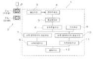
이하, 본 발명의 일 실시 형태에 대해 도면을 이용하여 설명한다. 도 1은 본 실시 형태에 있어서의 기판 검사 장치(1)의 블럭도를 나타내고, 도 2는 내측 영역 데이터 생성 수단(7)의 블럭도를 상세하게 나타낸 것이다. 또, 도 3은 프린트 기판(2)상에 형성된 패턴 영역과 검사 영역과의 관계를 나타내고, 도 3(a)은 기준으 로 되는 프린트 기판(이하 「기준 프린트 기판」이라고 칭함)(2a)과 내측 영역 및 외측 영역의 위치 관계를 나타내는 도면이다. 또, 도 3(b)은 검사 대상으로 되는 프린트 기판(2b)과 내측 영역 및 외측 영역의 관계를 나타내는 도면이다. 또한, 도 4는 내측 영역의 형성 상태를 판별할 때에 이용되는 히스토그램을 나타내는 도면이다. 또, 도 5는 외측 영역에 있어서의 위치-휘도 그래프를 나타내는 것이고, 이 좌표계에 있어서의 패턴 영역의 윤곽 부분의 위치를 산출하는 것이다. 또한, 도 6 및 도 7은 이 기판 검사 장치(1)의 동작을 나타내는 플로우차트를 나타낸 것이다.EMBODIMENT OF THE INVENTION Hereinafter, one Embodiment of this invention is described using drawing. FIG. 1 shows a block diagram of the
이 실시 형태에 있어서 기판 검사 장치(1)는 카메라 등의 촬상 수단(3)을 이용하여 프린트 기판(2)의 패턴 영역(20)(도 3 참조)의 화상을 취득하고, 그 패턴 영역(20)의 내측과 외측을 다른 검사 기준으로 검사하도록 한 것이다. 또한, 도 3에 있어서, 굵은 실선 및 그 내측이 프린트 기판(2)상에 형성된 패턴 영역(20)을 나타낸다. 이하, 본 실시 형태에 있어서의 기판 검사 장치(1)의 구성에 대하여 상세하게 설명한다.In this embodiment, the board |
도 1에 있어서, 촬상 수단(3)은 검사 대상으로 되는 프린트 기판(2), 또는 기준으로 되는 프린트 기판(2a)의 표면을 촬상하는 것으로, 이 실시 형태에서는 256 계조의 그레이 스케일(gray scale)에 의하여 그 표면의 화상을 취득한다.In FIG. 1, the imaging means 3 picks up the surface of the printed board |
전(前)처리 수단(4)은 이 CCD 카메라에 의하여 촬상된 프린트 기판(2)의 화상에 대하여 A/D 변환 등의 처리를 행하고, 이 처리된 데이터를 일단 화상 메모리(5)에 기억한다.The preprocessing means 4 performs an A / D conversion or the like process on the image of the printed
윤곽 추출 수단(6)은 전처리 수단(4)에서 처리된 화상 데이터로부터 패턴 영 역(20)의 윤곽(20a)을 추출하는 것으로, 취득된 256 계조의 그레이 스케일의 화상을 소정의 문턱값을 이용하여 2값화하고, 이 2값화된 화상에 대하여 흑에서 백으로, 또는 백에서 흑색으로 변화하는 부분을 윤곽(20a) 부분으로서 그 위치에 관한 데이터를 생성한다.The outline extracting means 6 extracts the
내측 영역 데이터 생성 수단(7)은 이 추출된 윤곽(20a) 부분을 내측으로 축소 처리하고, 도 3(a)의 내측 파선 부분의 내측 영역(21b)내(오른쪽 경사 아래 방향의 사선부)의 휘도에 관한 데이터를 생성한다. 구체적으로는 축소 처리된 내측 영역(21b)에 대한 히스토그램을 생성하고, 이 히스토그램 중에서, 미리 밝은 측과 어두운 측에 설정된 2 개의 기준값과 비교하기 위한 데이터를 생성한다. 도 2에, 이 내측 영역 데이터 생성 수단(7)의 상세한 블럭도를 나타낸다. 이 내측 영역 데이터 생성 수단(71)은 제1의 계수 수단(70)과, 히스토그램 수정 수단(71)과, 제2의 계수 수단(72)을 구비하여 이루어진다.The inner region data generating means 7 shrinks the extracted
이 중 제1의 계수 수단(70)은 이 화상 메모리(5)에 기억되어 있는 프린트 기판(2)의 화상 중에서, 예를 들면 휘도 150 에서 250 까지의 화소를 추출하여 각각 계수하고, 기준 프린트 기판(2a)의 히스토그램 및, 검사 대상으로 되는 프린트 기판(2b)의 히스토그램을 생성한다. 도 4(a)(b)(c)에 이 히스토그램을 나타낸다. 도 4(a)(b)(c)에 있어서, 가는 실선은 기준 프린트 기판(2a)의 히스토그램을 나타내고, 또 굵은 실선은 검사 대상으로 되는 프린트 기판(2b)의 히스토그램을 나타낸다. 그리고, 이 기준 프린트 기판(2a)의 히스토그램은 기억 수단(8)에 기억되고, 또한 검사 대상의 프린트 기판(2b)의 히스토그램에 대해서는 다음의 히스토그램 수 정 수단(71)에 의해 기재된 색, 레지스트의 색, 패드의 표면의 생채기의 유무 등에 근거하여 수정 처리가 이루어진다.Among these, the first counting means 70 extracts and counts, for example, pixels of
이 히스토그램 수정 수단(71)은 기준 프린트 기판(2a)에 대한 히스토그램의 기준 평균 휘도 Ave0을 산출하는 동시에, 검사 대상으로 되는 프린트 기판(2b)의 히스토그램의 평균 휘도 Ave1을 산출하고, 이 평균 휘도 Ave1을 Ave0에 합치(合致)시키도록 검사 대상의 프린트 기판(2b)의 각 휘도의 화소 수를 수정한다. 이것을 도 4(b)(c)의 굵은 실선으로 나타나는 히스토그램에 근거하여 설명하면, 우선 δ=Ave0-Avel 을 산출하고, 검사 대상으로 되는 프린트 기판(2b)의 각 화소의 휘도를 δ 만큼 시프트시키고, 굵은 실선의 히스토그램을 굵은 파선으로 나타나는 히스토그램에 시프트시킨다. 그리고, 이 수정된 히스토그램에 근거하여 기준 프린트 기판(2a)의 히스토그램에 비해 어느 정도 밝은 측으로 시프트하고 있는지를 나타내기 위한 데이터, 또는 어느 정도 어두운 측으로 시프트하고 있는지를 나타내기 위한 데이터인 내측 기준 데이터를 생성한다.The histogram correcting means 71 calculates the reference average luminance Ave0 of the histogram with respect to the reference printed
제2의 계수 수단(72)은 우선, 히스토그램의 시프트의 허용 범위를 나타내기 위한 내측 기준 데이터를 생성한다. 구체적으로는 도 4(a)에 나타내는 바와 같이, 기준 프린트 기판(2a)의 히스토그램에 대하여 미리 어두운 측에 설정된 제1의 휘도 P1의 화소 수를 계수하고, 그 화소 수에 휘도 150 에서부터 P1 까지의 휘도 폭을 곱한 값 S1(도 4에 있어서의 직사각 형상 면적 부분)을 연산하는 동시에, 제2의 휘도 P2에 대한 화소 수를 계수하고, 그 화소 수에 휘도 P2 에서부터 250 까지의 휘도 폭을 곱한 값 S2(동일하게 직사각 형상 면적 부분)를 연산한다. 그리고, 이것을 내측 기준 데이터로서 기억 수단(8)에 격납한다. 그리고, 검사 대상으로 되는 프린트 기판(2b)에 대해서는 수정된 히스토그램을 이용하여 상기 제1의 휘도 P1 보다 어두운 각 휘도의 화소 수를 각각 계수하여 가산하고, 이것을 S1' 로서 기억 수단(8)에 격납하는 동시에, 제2의 휘도 P2 보다 밝은 각 휘도의 화소 수를 각각 계수하여 가산하고, 이것을 S2'로 한다. 그리고, 이 S1', S1 및 S2', S2 를 이용하여 내측 영역(21b)의 형성 상태의 양부를 판정할 수 있도록 한다.The second counting means 72 firstly generates the inner reference data for indicating the allowable range of the shift of the histogram. Specifically, as shown in Fig. 4A, the number of pixels of the first luminance P1 set in advance on the dark side with respect to the histogram of the reference printed
내측 판정 수단(9)은 이 제2의 계수 수단(72)에 의하여 계수된 기준 프린트 기판(2a)의 내측 기준 데이터인 화소 수 S1ㆍS2 와, 검사 대상으로 되는 프린트 기판(2b)의 내측 검사 데이터인 화소 수 S1'ㆍS2' 를 비교한다. 그리고, 화소 수 S1보다 S1'의 쪽이 큰 경우는 불량품인 취지를 출력 수단(12)을 통하여 출력하고, 또 화소 수 S2보다 S2'의 쪽이 큰 경우도 이와 같이 불량품인 취지를 출력 수단을 통하여 출력한다.The inner determination means 9 checks the number of pixels S1 and S2 which are the inner reference data of the reference printed
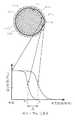
다음에, 외측 영역 데이터 생성 수단(10)의 구성에 대하여 설명한다. 외측 영역 데이터 생성 수단(10)은 패턴 영역(20)의 윤곽(20a) 부분의 형성 상태를 판정하기 위한 데이터를 생성하는 것으로, 기준으로 되는 외측 영역 데이터(이하, 「외측 기준 데이터」라고 칭함)와, 검사 대상의 프린트 기판(2b)의 외측 검사 데이터를 생성한다. 도 3을 이용하여 이 외측 영역 데이터 생성 수단(10)의 처리의 개요를 나타낸다.Next, the configuration of the outer area data generating means 10 will be described. The outer region
외측 영역 데이터 생성 수단(10)은 우선, 외측 기준 데이터를 생성하기 위하여, 도 3(a)의 외측 파선 부분에 나타내는 바와 같이 윤곽(20a)을 외측에 확대 처 리하는 동시에, 상기 윤곽 추출 수단(6)에서 추출된 윤곽(20a) 부분에 대한 스플라인(spline)(20b)를 생성하고, 그 스플라인(20b)의 법선 방향(20c)에 있어서의 상기 내측 영역(21b)과 확대 처리된 윤곽(22a)과 사이의 영역(이하 「링 형상 영역」이라고 칭함)(22b)에 있어서의 휘도에 관한 그래프를 생성한다. 도 5에 이 위치-휘도에 관한 그래프를 나타낸다. 도 5에 있어서, 원점은 내측 영역(21b)의 윤곽(20a) 부분으로 설정되고, 외측 영역의 방향을 플러스측에 설정하고 있다. 통상, 패턴 영역(20)의 내측은 금속으로 형성되어 있기 때문에 휘도가 높아지고, 반대로 패턴 영역(20)의 외측은 레지스트 등으로 형성되어 있기 때문에 휘도가 작아진다. 그리고, 이 그래프의 변곡점이 패턴 영역(20)의 윤곽(20a) 부분으로 된다. 그리고, 외측 영역 데이터 생성 수단(10)은 스플라인(20b) 방향으로 수 화소씩 옮긴 모든 좌표계에 있어서의 변곡점을 검출하고, 이것을 외측 기준 데이터로서 기억 수단(8)에 격납한다.The outer region data generating means 10 first enlarges and processes the
다음에, 이 외측 영역 데이터 생성 수단(10)은 검사 대상으로 되는 프린트 기판(2b)의 외측 검사 데이터를 생성한다. 구체적으로는, 도 3(b)에 나타내는 바와 같이 상기 링 형상 영역(22b)을 검사 대상의 패턴 영역(20)에 중합(重合)하고, 도 5에 나타내는 바와 같이 상기 스플라인(20b)의 법선 방향(20c)의 휘도에 관한 그래프를 생성한다. 그리고, 그 그래프의 변곡점 x, 즉 검사 대상으로 되는 패턴 영역(20)의 이 좌표계에 있어서의 윤곽(20a)의 위치를 검출하고, 스플라인(20b) 방향으로 수 화소씩 옮긴 각각의 좌표계에 있어서의 변곡점 x의 위치를 검출하고 외측 검사 데이터를 생성한다.Next, this outer region
외측 판정 수단(11)은 이와 같이 생성된 외측 기준 데이터와 외측 검사 데이터를 비교하고, 각 법선 방향(20c)에 있어서의 각각의 변곡점 x0, x의 거리 |x-x0| 가 미리 정해진 기준값 δ0 내에 있는지의 여부를 판정한다. 그리고, |x-x0|>δ0 인 경우는 윤곽(20a) 부분에 흠이나 돌출 부분을 생기고 있다고 하여 불량품인 취지를 출력 수단(12)을 통하여 출력하고, 또 |x-x0|
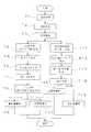
다음에, 이와 같이 구성된 기판 검사 장치(1)의 처리 플로우에 대하여 도 6, 도 7을 이용하여 설명한다. 우선, 도 6에 검사 대상으로 되는 프린트 기판(2b)을 검사할 때에 필요한 기준 데이터를 생성하는 플로우를 나타내고, 도 7에 검사 대상으로 되는 프린트 기판(2b)을 검사하는 경우의 플로우를 나타낸다.Next, the processing flow of the board |
<내측 기준 데이터의 생성 및 외측 기준 데이터의 생성 플로우><Generation of Inner Reference Data and Generation of Outer Reference Data>
우선, 내측 기준 데이터를 생성하는 경우, 기준 프린트 기판(2a)을, 그 표면에 형성된 나타내지 않은 기준 마크 등을 이용하여 소정의 기판 검사 장치(1)의 위치에 장착하고, 촬상 수단(3)을 이용하여 그 기준 프린트 기판(2a)의 표면의 화상을 취득한다(단계 S1). 그리고, 이 취득된 화상을 전처리 수단(4)에 의하여 A/D 변환하고(단계 S2), 그 변환한 화상 정보를 화상 메모리(5)에 기입한다. 그리고, 이와 같이 취득된 화상을 소정의 휘도값을 이용하여 2값화하고, 흑색에서 백으로, 또는 백에서 흑으로 변화하는 부분을 윤곽(20a) 부분으로서 기억 수단(8)에 격납한다(단계 S3).First, when generating the inner reference data, the reference printed
다음에, 이 윤곽(20a) 부분에 대하여 축소 처리를 행하고(단계 S4), 이 축소된 내측 영역(21b)에 대하여 256 계조의 그레이 스케일 중 휘도 150 에서부터 250 까지의 휘도의 각 화소 수를 계수하고, 도 4(a)에 나타내는 히스토그램을 생성한다(단계 S5). 그 다음에, 우선 이 생성된 히스토그램으로부터 기준 평균 휘도 Ave0 을 구한다(단계 S6). 그리고, 미리 설정된 제1의 휘도 P1 및 제2의 휘도 P2 에 대하여, 그 제1의 휘도 P1ㆍ제2의 휘도 P2 의 화소 수를 계수하고, 제1의 휘도 P1의 화소 수에 휘도 150 에서부터 P1 까지의 휘도 폭을 곱한 화소 수 S1, 및 제2의 휘도 P2 의 화소 수에 휘도 P2 에서부터 250 까지의 휘도 폭을 곱한 화소 수 S2 를 연산하고(단계 S7), 이러한 화소 수 S1ㆍS2 를 내측 기준 데이터로서 기억 수단(8)에 격납한다(단계 S8).Next, a reduction process is performed on the portion of the
다음에, 외측 기준 데이터를 생성할 때는 우선, 윤곽(20a) 부분에 대하여 확대 처리를 행하고(단계 S9), 축소 영역에서 외측의 링 상태 영역(22b)의 화소에 관한 정보를 수집한다. 그리고, 도 5에 나타내는 바와 같이, 윤곽(20a)의 스플라인(20b)의 법선 방향(20c)에 대한 위치-휘도 그래프를 생성하고(단계 S10), 이 그래프 중에서, 휘도의 미분값이 가장 크게 변화하는 변곡점의 위치 x0 을 연산한다. 그리고, 이것을 스플라인(20b) 방향으로 수 화소씩 옮긴 각 좌표계에 있어서의 변곡점의 위치에 관한 정보를 외측 기준 데이터로서 기억 수단(8)에 격납한다(단계 S11).Next, when generating the outer reference data, first, an enlargement process is performed on the
그리고, 이 기준 프린트 기판(2a)을 기판 검사 장치(1)로부터 떼어내고, 검사 대상으로 되는 프린트 기판(2b)의 검사를 행하게 한다.And this reference printed
<검사 대상으로 되는 프린트 기판(2)의 검사 처리><Inspection process of the printed
다음에, 검사 대상으로 되는 프린트 기판(2b)의 형성 상태를 검사하는 경우, 동일하게 하여 우선 기준 마크를 이용하여 기판 검사 장치(1)의 소정의 위치에 장착하고, 그 프린트 기판(2b)의 표면의 화상을 취득한다(단계 T1). 그리고, 이 취득된 화상을 전처리 수단(41)에 의해 A/D 변환하고(단계 T2), 그 정보를 화상 메모리(5)에 기입한다.Next, in the case of inspecting the formation state of the printed
그리고, 이미 기억 수단(8)에 격납되어 있는 기준 프린트 기판(2a)의 내측 영역(21b)의 위치 정보를 독출하고, 이것을 검사 대상으로 되는 프린트 기판(2b)의 패턴 영역(20)에 중합하고(단계 T3), 그 내측의 화소에 관한 정보를 수집한다. 그리고, 동일하게, 이 영역에 대하여 256 계조의 그레이 스케일에서 휘도 150 에서부터 250 까지의 휘도의 화소 수를 계수하고, 도 4(b)(c)의 굵은 실선으로 나타내는 히스토그램을 생성하는 동시에(단계 T4), 이 생성된 히스토그램으로부터 평균 휘도 Ave1 을 산출한다(단계 T5). 그 다음에, 이 산출된 평균 휘도 Ave1 과 상기 기준 프린트 기판(2a)의 기준 평균 휘도 Ave0 과의 차 δ을 계산하고, 단계 T3에서 생성된 히스토그램의 각 휘도를 이 δ 만큼 시프트시킨 수정 처리를 행한다(단계 T6). 그리고, 이 수정된 히스토그램에 근거하여, 미리 설정되어 있는 제1의 휘도 P1 보다 어두운 휘도의 각 화소 수 S1' 을 계수하는 동시에, 제2의 휘도 P2 보다 밝은 휘도의 각국 소수 S2' 를 계수하고(단계 T7), 내측 기준 데이터 S1, S2 와의 판정에 의해(단계 T8), 그 프린트 기판(2b)이 불량품인 취지의 출력을 행한다(단계 T9). 또, 검사 대상으로 되는 프린트 기판(2b)의 화소 수 S2'가 기준 프린트 기 판(2a)의 화소 수 S2 보다 큰 경우도 동일하게(단계 T7), 그 프린트 기판(2b)에 대하여 불량품인 취지의 출력을 행한다(단계 T9). 즉, 제1의 기준 화소 수 S1 보다 S1' 의 쪽이 큰 경우는 연마에 의한 상처 이상으로 결손을 생기게 할 가능성이 높기 때문에, 이것을 불량품이라고 판정하고, 또 제2의 기준 화소 수 S2 보다 S2' 의 쪽이 큰 경우는 패드에 돌기 등이 존재하고 있을 가능성이 높기 때문에, 이것을 불량품으로 판정한다. 한편, S1'

다음에, 윤곽(20a) 부분의 형성 상태를 검사하기 위하여, 기준 프린트 기판(2a)의 링 형상 영역(22b)을 검사 대상의 패턴 영역(20b)에 중합시킨 링 형상 영역내(22b)의 화소에 관한 정보를 수집한다(단계 T11). 그리고, 이 링 형상 영역(22b)에 대하여, 기준 프린트 기판(2a)의 스플라인(20b)의 법선 방향(20c)의 휘도에 관한 위치-휘도 그래프를 생성하고(단계 T12), 그 그래프에 있어서의 변곡점을 검출한다(단계 T13). 이와 동일한 처리를 스플라인(20b) 방향으로 수 화소씩 옮겨서 행하고, 이 검출된 변곡점의 위치 x와 이미 기억 수단(8)에 격납되어 있는 변곡점의 위치 x0 와의 거리 δ0 와의 비교 판정을 행하고(단계 T14), 이 거리가 소정의 문턱값 δ0 을 초과하고 있는 경우는 불량품인 취지의 출력을 행하고(단계 T15), 또한 이 검출된 변곡점의 위치와 이미 기억 수단(8)에 격납되어 있는 변곡점과의 거리가 소정의 문턱값 δ0 의 범위내인 경우는 우량품인 취지의 출력을 행한다(단계 T16).Next, in order to inspect the formation state of the part of the
이와 같이 상기 실시 형태에 의하면, 프린트 기판(2b)상에 형성된 패드나 배 선 패턴 등의 패턴 영역(20)의 형성 상태를 검사하는 기판 검사 장치(1)에 있어서, 검사 대상으로 되는 패턴 영역(20)의 내측 영역(21b)의 검사 데이터를 생성하는 내측 영역 데이터 생성 수단(7)과, 외측의 링 형상 영역(22b)의 검사 데이터를 생성하는 외측 영역 데이터 소성 수단(10)과, 이 생성된 내측 영역 데이터와 미리 설정된 내측 기준 데이터를 비교하는 동시에, 외측 영역 데이터와 외측 기준 데이터를 비교함으로써, 이 패턴 영역(20)의 양부를 판정하는 내측 판정 수단(9)ㆍ외측 판정 수단(11)을 설치하도록 하였으므로, 비교적 큰 결함이 허용되는 패턴 영역(20)의 내측 영역(21b)에 대해서는 완만한 검사 기준을 적용하고, 또 미세한 결함도 문제로 되는 패턴 영역(20)의 링 형상 영역(22b)에 대해서는 어려운 검사 기준을 적용함으로써, 프린트 기판(2b)의 결함 검출을 정밀하고 양호한 효율로 행할 수 있게 된다.Thus, according to the said embodiment, in the board | substrate test |
또, 이 실시 형태에서는 내측 영역 데이터의 종류를, 휘도에 관한 데이터, 즉 히스토그램의 시프트를 나타내는 데이터로 하였으므로, 내측 영역(21b)의 생채기나 얼룩짐 등을 정확하게 검사할 수 있고, 또 외측 영역 데이터의 종류를 윤곽(20a)의 위치에 관한 데이터로 하였으므로, 윤곽(20a) 부분에 있어서의 패드의 흠이나 돌출 부분 등을 정확하게 검사할 수 있게 된다.In this embodiment, since the type of the inner region data is set as data relating to luminance, that is, data indicating a shift in the histogram, rawness, unevenness, and the like of the
또한, 본 발명은 상기 실시 형태로 한정되는 일 없이, 여러 가지의 형태로 행하는 것이 가능하다.In addition, this invention can be performed in various forms, without being limited to the said embodiment.
예를 들면, 상기 실시 형태에서는 프린트 기판(2)의 검사를 예로 들어 설명하였으나, 이것에 한정하지 않고, 유리 기판의 패턴을 검사하는 경우에 대해서도 적용할 수 있다.For example, in the said embodiment, although the test | inspection of the printed
또, 상기 실시 형태에서는 내측 영역 데이터로서 히스토그램의 시프트를 나타내는 데이터로 하고, 또 외측 영역 데이터로서 패턴 영역(20)의 윤곽(20a)의 위치를 나타내는 데이터로 하였으나, 이것에 한정하지 않고, 내측과 외측의 영역을 다른 기준값을 이용하여 검사하는 방법이면, 어떠한 방법을 채용해도 좋다.In the above embodiment, data indicating the shift of the histogram is used as the inner region data, and data indicating the position of the
프린트 기판(1)상에 형성된 패턴 영역(20)의 형성 상태를 검사하는 경우, 패턴 영역(20)의 내측 영역(21c)과 외측의 링 형상 영역(22b)을 각각 별도로 검사하는 것으로, 비교적 큰 결함이 허용되는 패턴 영역(20)의 내측에 대하여 완만한 기준을 적용하고, 또 미세한 결함도 문제로 되는 패턴 영역(20)의 외측에 대하여 어려운 기준을 적용할 수 있다. 또, 특히 링 형상 영역(22b)에 대해서는 형상에 관한 판정 기준을 이용하여 검사하므로, 인접하는 패턴 영역(20)과의 단락 등을 방지할 수 있다.In the case of inspecting the formation state of the
도 1은 본 발명의 일 실시 형태에 있어서의 기판 검사 장치의 블럭도.BRIEF DESCRIPTION OF THE DRAWINGS The block diagram of the board | substrate inspection apparatus in one Embodiment of this invention.
도 2는 동일 형태에 있어서의 내측 영역 데이터 생성 수단의 상세 블럭도.Fig. 2 is a detailed block diagram of inner region data generating means in the same form.
도 3은 동일 형태에 있어서의 패턴 영역과 검사 영역과의 관계를 나타내는 도면.3 is a diagram illustrating a relationship between a pattern region and an inspection region in the same form.
도 4는 동일 형태에 있어서의 내측 영역의 히스토그램(histogram)을 나타내는 도면.4 shows a histogram of an inner region in the same form.
도 5는 동일 형태에 있어서의 외측 영역의 위치-휘도 그래프를 나타내는 도면.Fig. 5 is a diagram showing a position-luminance graph of an outer region in the same form.
도 6은 동일 형태에 있어서의 기준 데이터를 생성하기 위한 플로우차트.6 is a flowchart for generating reference data in the same form.
도 7은 동일 형태에 있어서의 프린트 기판을 검사할 때의 플로우차트.7 is a flowchart for inspecting a printed board in the same embodiment.
<부호의 설명><Description of the code>
1ㆍㆍㆍ기판 검사 장치1 ... board inspection apparatus
2a, 2bㆍㆍㆍ프린트 기판2a, 2b ... printed board
(2a:기준 프린트 기판, 2b:검사 대상으로 되는 프린트 기판)(2a: reference printed board, 2b: printed board to be inspected)
7ㆍㆍㆍ내측 영역 데이터 생성 수단7. Inner area data generating means
9ㆍㆍㆍ내측 판정 수단9 ... inside determination means
10ㆍㆍㆍ외측 영역 데이터 생성 수단10 ... outer area data generating means
11ㆍㆍㆍ외측 판정 수단11 ... outside determination means
20ㆍㆍㆍ패턴 영역20 pattern areas
21aㆍㆍㆍ내측 영역의 윤곽21a ... contour of the inner region
21bㆍㆍㆍ내측 영역21b ... inner region
22aㆍㆍㆍ외측 영역의 윤곽22a ... contour of outer region
22bㆍㆍㆍ링(ring) 형상 영역22b ... ring-shaped region
Claims (2)
Translated fromKoreanApplications Claiming Priority (2)
| Application Number | Priority Date | Filing Date | Title |
|---|---|---|---|
| JPJP-P-2003-00425497 | 2003-12-22 | ||
| JP2003425497AJP3589424B1 (en) | 2003-12-22 | 2003-12-22 | Board inspection equipment |
Related Parent Applications (1)
| Application Number | Title | Priority Date | Filing Date |
|---|---|---|---|
| KR1020067014526ADivisionKR100827906B1 (en) | 2003-12-22 | 2004-12-17 | Substrate inspection device |
Publications (2)
| Publication Number | Publication Date |
|---|---|
| KR20080011235A KR20080011235A (en) | 2008-01-31 |
| KR101022187B1true KR101022187B1 (en) | 2011-03-17 |
Family
ID=33509216
Family Applications (2)
| Application Number | Title | Priority Date | Filing Date |
|---|---|---|---|
| KR1020067014526AExpired - LifetimeKR100827906B1 (en) | 2003-12-22 | 2004-12-17 | Substrate inspection device |
| KR1020077030048AExpired - Fee RelatedKR101022187B1 (en) | 2003-12-22 | 2004-12-17 | Substrate inspection device |
Family Applications Before (1)
| Application Number | Title | Priority Date | Filing Date |
|---|---|---|---|
| KR1020067014526AExpired - LifetimeKR100827906B1 (en) | 2003-12-22 | 2004-12-17 | Substrate inspection device |
Country Status (5)
| Country | Link |
|---|---|
| US (1) | US7639860B2 (en) |
| JP (1) | JP3589424B1 (en) |
| KR (2) | KR100827906B1 (en) |
| CN (1) | CN1898555B (en) |
| WO (1) | WO2005062028A1 (en) |
Families Citing this family (13)
| Publication number | Priority date | Publication date | Assignee | Title |
|---|---|---|---|---|
| US8588511B2 (en)* | 2002-05-22 | 2013-11-19 | Cognex Corporation | Method and apparatus for automatic measurement of pad geometry and inspection thereof |
| JP4610182B2 (en)* | 2003-12-05 | 2011-01-12 | 株式会社日立ハイテクノロジーズ | Scanning electron microscope |
| JP4518494B2 (en)* | 2005-03-28 | 2010-08-04 | 大日本スクリーン製造株式会社 | Land pattern inspection method and inspection apparatus |
| US8200042B2 (en)* | 2007-01-31 | 2012-06-12 | Olympus Corporation | Endoscope apparatus and program |
| JP5295526B2 (en)* | 2007-01-31 | 2013-09-18 | オリンパス株式会社 | Endoscope device for measurement |
| JP2008286692A (en)* | 2007-05-18 | 2008-11-27 | Mega Trade:Kk | Appearance inspection system |
| JP5137926B2 (en)* | 2009-09-29 | 2013-02-06 | 日立建機株式会社 | Cylinder block spool hole inspection method |
| DE102010060375A1 (en)* | 2010-11-05 | 2012-05-10 | Hseb Dresden Gmbh | inspection procedures |
| FR3059423B1 (en)* | 2016-11-29 | 2020-05-29 | Vit | SYSTEM AND METHOD FOR OPTICAL POSITIONING AND INSPECTION OF AN OBJECT |
| JP6958345B2 (en)* | 2017-12-27 | 2021-11-02 | 株式会社デンソー | Visual inspection equipment |
| CN109900711A (en)* | 2019-04-02 | 2019-06-18 | 天津工业大学 | Workpiece defect detection method based on machine vision |
| CN114549390A (en)* | 2020-11-25 | 2022-05-27 | 鸿富锦精密电子(成都)有限公司 | Circuit board detection method, electronic device and storage medium |
| CN114429102B (en)* | 2021-12-31 | 2025-09-02 | 杭州电子科技大学 | A rapid detection method for the minimum allowable range between elements in PCB board AOI |
Citations (2)
| Publication number | Priority date | Publication date | Assignee | Title |
|---|---|---|---|---|
| JPH11337498A (en)* | 1998-05-26 | 1999-12-10 | Dainippon Screen Mfg Co Ltd | Apparatus and method for inspecting printed circuit board |
| JP2000241130A (en)* | 1999-02-23 | 2000-09-08 | Fujitsu Ltd | Pattern inspection method and apparatus |
Family Cites Families (15)
| Publication number | Priority date | Publication date | Assignee | Title |
|---|---|---|---|---|
| US4783826A (en)* | 1986-08-18 | 1988-11-08 | The Gerber Scientific Company, Inc. | Pattern inspection system |
| JPS63196980A (en) | 1987-02-10 | 1988-08-15 | Toshiba Corp | Printed circuit board soldering appearance inspection equipment |
| JPH01114324A (en) | 1987-10-26 | 1989-05-08 | Hitachi Ltd | Selective ground fault relay device |
| JP2502853B2 (en) | 1991-09-05 | 1996-05-29 | 松下電器産業株式会社 | Wiring pattern inspection device |
| US5555316A (en)* | 1992-06-30 | 1996-09-10 | Matsushita Electric Industrial Co., Ltd. | Inspecting apparatus of mounting state of component or printing state of cream solder in mounting line of electronic component |
| JPH0658729A (en) | 1992-08-12 | 1994-03-04 | Fujitsu Ltd | Inspecting apparatus for soldered state |
| US5608816A (en)* | 1993-12-24 | 1997-03-04 | Matsushita Electric Industrial Co., Ltd. | Apparatus for inspecting a wiring pattern according to a micro-inspection and a macro-inspection performed in parallel |
| JPH10187977A (en)* | 1996-12-25 | 1998-07-21 | Fujitsu Ltd | Pattern inspection method and apparatus |
| US6330354B1 (en)* | 1997-05-01 | 2001-12-11 | International Business Machines Corporation | Method of analyzing visual inspection image data to find defects on a device |
| JPH1114324A (en) | 1997-06-27 | 1999-01-22 | Hitachi Ltd | Pattern defect inspection method and apparatus |
| JP2000283929A (en)* | 1999-03-31 | 2000-10-13 | Fujitsu Ltd | Wiring pattern inspection method and apparatus |
| CA2296143A1 (en)* | 2000-01-18 | 2001-07-18 | 9071 9410 Quebec Inc. | Optical inspection system |
| US7058221B1 (en)* | 2000-07-07 | 2006-06-06 | Tani Electronics Industry Co., Ltd. | Method of recognizing object based on pattern matching and medium for recording computer program having same |
| JP2003086919A (en) | 2001-09-07 | 2003-03-20 | Sun Tec Kk | Pattern inspection device |
| JP3993817B2 (en)* | 2002-12-11 | 2007-10-17 | 株式会社日立製作所 | Defect composition analysis method and apparatus |
- 2003
- 2003-12-22JPJP2003425497Apatent/JP3589424B1/ennot_activeExpired - Fee Related
- 2004
- 2004-12-17KRKR1020067014526Apatent/KR100827906B1/ennot_activeExpired - Lifetime
- 2004-12-17CNCN2004800385032Apatent/CN1898555B/ennot_activeExpired - Fee Related
- 2004-12-17USUS10/583,660patent/US7639860B2/ennot_activeExpired - Fee Related
- 2004-12-17KRKR1020077030048Apatent/KR101022187B1/ennot_activeExpired - Fee Related
- 2004-12-17WOPCT/JP2004/018947patent/WO2005062028A1/enactiveApplication Filing
Patent Citations (2)
| Publication number | Priority date | Publication date | Assignee | Title |
|---|---|---|---|---|
| JPH11337498A (en)* | 1998-05-26 | 1999-12-10 | Dainippon Screen Mfg Co Ltd | Apparatus and method for inspecting printed circuit board |
| JP2000241130A (en)* | 1999-02-23 | 2000-09-08 | Fujitsu Ltd | Pattern inspection method and apparatus |
Also Published As
| Publication number | Publication date |
|---|---|
| KR100827906B1 (en) | 2008-05-07 |
| CN1898555B (en) | 2011-09-14 |
| US7639860B2 (en) | 2009-12-29 |
| JP2005181218A (en) | 2005-07-07 |
| KR20080011235A (en) | 2008-01-31 |
| KR20060130109A (en) | 2006-12-18 |
| JP3589424B1 (en) | 2004-11-17 |
| WO2005062028A1 (en) | 2005-07-07 |
| US20070147676A1 (en) | 2007-06-28 |
| CN1898555A (en) | 2007-01-17 |
Similar Documents
| Publication | Publication Date | Title |
|---|---|---|
| US7260244B2 (en) | Print inspection method and print inspection apparatus | |
| TWI412739B (en) | Defect detection method and defect detection apparatus | |
| JP2004509325A (en) | Reduce false alarms in PCB inspection | |
| US20070053580A1 (en) | Image defect inspection apparatus, image defect inspection system, defect classifying apparatus, and image defect inspection method | |
| KR101022187B1 (en) | Substrate inspection device | |
| KR20110040965A (en) | Appearance inspection device | |
| JP4230880B2 (en) | Defect inspection method | |
| CN113935927A (en) | Detection method, device and storage medium | |
| JP4910128B2 (en) | Defect inspection method for object surface | |
| JP2000163579A (en) | Appearance inspection method and apparatus | |
| JP4841819B2 (en) | Defect detection by color image of an object | |
| JP3536884B2 (en) | Semiconductor wafer defect classification method and apparatus | |
| JP4244046B2 (en) | Image processing method and image processing apparatus | |
| JP4275582B2 (en) | Board inspection equipment | |
| JP4084257B2 (en) | Printed circuit board inspection equipment | |
| JP2002267619A (en) | Defect inspection method and device | |
| JP4474006B2 (en) | Inspection device | |
| JP4745633B2 (en) | Defect detection method and apparatus using color image of object | |
| JP2004226212A (en) | Method and device for detecting pinhole defect and contamination defect on transparent object | |
| JP2005091330A (en) | Color tone inspection apparatus and method, and light stain inspection apparatus and method | |
| JP4889018B2 (en) | Appearance inspection method | |
| JP2529505B2 (en) | Wiring pattern inspection device | |
| JPH1051199A (en) | Inspection method for mounting direction of electronic components | |
| CN120752518A (en) | Image processing method | |
| JP2005081544A (en) | Print defect inspection device for printed matter |
Legal Events
| Date | Code | Title | Description |
|---|---|---|---|
| A107 | Divisional application of patent | ||
| A201 | Request for examination | ||
| PA0104 | Divisional application for international application | St.27 status event code:A-0-1-A10-A16-div-PA0104 St.27 status event code:A-0-1-A10-A18-div-PA0104 | |
| PA0201 | Request for examination | St.27 status event code:A-1-2-D10-D11-exm-PA0201 | |
| PG1501 | Laying open of application | St.27 status event code:A-1-1-Q10-Q12-nap-PG1501 | |
| E902 | Notification of reason for refusal | ||
| PE0902 | Notice of grounds for rejection | St.27 status event code:A-1-2-D10-D21-exm-PE0902 | |
| P11-X000 | Amendment of application requested | St.27 status event code:A-2-2-P10-P11-nap-X000 | |
| P13-X000 | Application amended | St.27 status event code:A-2-2-P10-P13-nap-X000 | |
| E601 | Decision to refuse application | ||
| PE0601 | Decision on rejection of patent | St.27 status event code:N-2-6-B10-B15-exm-PE0601 | |
| T11-X000 | Administrative time limit extension requested | St.27 status event code:U-3-3-T10-T11-oth-X000 | |
| J201 | Request for trial against refusal decision | ||
| PJ0201 | Trial against decision of rejection | St.27 status event code:A-3-3-V10-V11-apl-PJ0201 | |
| J301 | Trial decision | Free format text:TRIAL DECISION FOR APPEAL AGAINST DECISION TO DECLINE REFUSAL REQUESTED 20081209 Effective date:20101231 | |
| PJ1301 | Trial decision | Decision date:20101231 Appeal event data comment text:Appeal Kind Category : Appeal against decision to decline refusal, Appeal Ground Text : 2007 7030048 Appeal request date:20081209 Appellate body name:Patent Examination Board Decision authority category:Office appeal board Decision identifier:2008101013096 St.27 status event code:A-3-3-V10-V15-crt-PJ1301 | |
| PS0901 | Examination by remand of revocation | St.27 status event code:A-6-3-E10-E12-rex-PS0901 | |
| S901 | Examination by remand of revocation | ||
| GRNO | Decision to grant (after opposition) | ||
| PS0701 | Decision of registration after remand of revocation | St.27 status event code:A-3-4-F10-F13-rex-PS0701 | |
| R18-X000 | Changes to party contact information recorded | St.27 status event code:A-3-3-R10-R18-oth-X000 | |
| PN2301 | Change of applicant | St.27 status event code:A-3-3-R10-R11-asn-PN2301 St.27 status event code:A-3-3-R10-R13-asn-PN2301 | |
| GRNT | Written decision to grant | ||
| PR0701 | Registration of establishment | St.27 status event code:A-2-4-F10-F11-exm-PR0701 | |
| PR1002 | Payment of registration fee | Fee payment year number:1 St.27 status event code:A-2-2-U10-U12-oth-PR1002 | |
| PG1601 | Publication of registration | St.27 status event code:A-4-4-Q10-Q13-nap-PG1601 | |
| LAPS | Lapse due to unpaid annual fee | ||
| PC1903 | Unpaid annual fee | Not in force date:20140308 Payment event data comment text:Termination Category : DEFAULT_OF_REGISTRATION_FEE St.27 status event code:A-4-4-U10-U13-oth-PC1903 | |
| PC1903 | Unpaid annual fee | Ip right cessation event data comment text:Termination Category : DEFAULT_OF_REGISTRATION_FEE Not in force date:20140308 St.27 status event code:N-4-6-H10-H13-oth-PC1903 | |
| P22-X000 | Classification modified | St.27 status event code:A-4-4-P10-P22-nap-X000 | |
| P22-X000 | Classification modified | St.27 status event code:A-4-4-P10-P22-nap-X000 |