KR101022087B1 - Touch screen panel - Google Patents
Touch screen panelDownload PDFInfo
- Publication number
- KR101022087B1 KR101022087B1KR1020090003644AKR20090003644AKR101022087B1KR 101022087 B1KR101022087 B1KR 101022087B1KR 1020090003644 AKR1020090003644 AKR 1020090003644AKR 20090003644 AKR20090003644 AKR 20090003644AKR 101022087 B1KR101022087 B1KR 101022087B1
- Authority
- KR
- South Korea
- Prior art keywords
- sensing
- patterns
- connection
- touch screen
- screen panel
- Prior art date
- Legal status (The legal status is an assumption and is not a legal conclusion. Google has not performed a legal analysis and makes no representation as to the accuracy of the status listed.)
- Active
Links
Images


Classifications
- G—PHYSICS
- G06—COMPUTING OR CALCULATING; COUNTING
- G06F—ELECTRIC DIGITAL DATA PROCESSING
- G06F3/00—Input arrangements for transferring data to be processed into a form capable of being handled by the computer; Output arrangements for transferring data from processing unit to output unit, e.g. interface arrangements
- G06F3/01—Input arrangements or combined input and output arrangements for interaction between user and computer
- G06F3/03—Arrangements for converting the position or the displacement of a member into a coded form
- G06F3/041—Digitisers, e.g. for touch screens or touch pads, characterised by the transducing means
- G06F3/044—Digitisers, e.g. for touch screens or touch pads, characterised by the transducing means by capacitive means
- G06F3/0443—Digitisers, e.g. for touch screens or touch pads, characterised by the transducing means by capacitive means using a single layer of sensing electrodes
- G—PHYSICS
- G06—COMPUTING OR CALCULATING; COUNTING
- G06F—ELECTRIC DIGITAL DATA PROCESSING
- G06F3/00—Input arrangements for transferring data to be processed into a form capable of being handled by the computer; Output arrangements for transferring data from processing unit to output unit, e.g. interface arrangements
- G06F3/01—Input arrangements or combined input and output arrangements for interaction between user and computer
- G06F3/03—Arrangements for converting the position or the displacement of a member into a coded form
- G06F3/041—Digitisers, e.g. for touch screens or touch pads, characterised by the transducing means
- G06F3/044—Digitisers, e.g. for touch screens or touch pads, characterised by the transducing means by capacitive means
- G06F3/0446—Digitisers, e.g. for touch screens or touch pads, characterised by the transducing means by capacitive means using a grid-like structure of electrodes in at least two directions, e.g. using row and column electrodes
- G—PHYSICS
- G02—OPTICS
- G02F—OPTICAL DEVICES OR ARRANGEMENTS FOR THE CONTROL OF LIGHT BY MODIFICATION OF THE OPTICAL PROPERTIES OF THE MEDIA OF THE ELEMENTS INVOLVED THEREIN; NON-LINEAR OPTICS; FREQUENCY-CHANGING OF LIGHT; OPTICAL LOGIC ELEMENTS; OPTICAL ANALOGUE/DIGITAL CONVERTERS
- G02F1/00—Devices or arrangements for the control of the intensity, colour, phase, polarisation or direction of light arriving from an independent light source, e.g. switching, gating or modulating; Non-linear optics
- G02F1/01—Devices or arrangements for the control of the intensity, colour, phase, polarisation or direction of light arriving from an independent light source, e.g. switching, gating or modulating; Non-linear optics for the control of the intensity, phase, polarisation or colour
- G02F1/13—Devices or arrangements for the control of the intensity, colour, phase, polarisation or direction of light arriving from an independent light source, e.g. switching, gating or modulating; Non-linear optics for the control of the intensity, phase, polarisation or colour based on liquid crystals, e.g. single liquid crystal display cells
- G02F1/133—Constructional arrangements; Operation of liquid crystal cells; Circuit arrangements
- G02F1/1333—Constructional arrangements; Manufacturing methods
- G02F1/13338—Input devices, e.g. touch panels
- G—PHYSICS
- G06—COMPUTING OR CALCULATING; COUNTING
- G06F—ELECTRIC DIGITAL DATA PROCESSING
- G06F3/00—Input arrangements for transferring data to be processed into a form capable of being handled by the computer; Output arrangements for transferring data from processing unit to output unit, e.g. interface arrangements
- G06F3/01—Input arrangements or combined input and output arrangements for interaction between user and computer
- G06F3/03—Arrangements for converting the position or the displacement of a member into a coded form
- G06F3/041—Digitisers, e.g. for touch screens or touch pads, characterised by the transducing means
- G06F3/0412—Digitisers structurally integrated in a display
- G—PHYSICS
- G06—COMPUTING OR CALCULATING; COUNTING
- G06F—ELECTRIC DIGITAL DATA PROCESSING
- G06F2203/00—Indexing scheme relating to G06F3/00 - G06F3/048
- G06F2203/041—Indexing scheme relating to G06F3/041 - G06F3/045
- G06F2203/04103—Manufacturing, i.e. details related to manufacturing processes specially suited for touch sensitive devices
- G—PHYSICS
- G06—COMPUTING OR CALCULATING; COUNTING
- G06F—ELECTRIC DIGITAL DATA PROCESSING
- G06F2203/00—Indexing scheme relating to G06F3/00 - G06F3/048
- G06F2203/041—Indexing scheme relating to G06F3/041 - G06F3/045
- G06F2203/04111—Cross over in capacitive digitiser, i.e. details of structures for connecting electrodes of the sensing pattern where the connections cross each other, e.g. bridge structures comprising an insulating layer, or vias through substrate
Landscapes
- Engineering & Computer Science (AREA)
- General Engineering & Computer Science (AREA)
- Theoretical Computer Science (AREA)
- Physics & Mathematics (AREA)
- General Physics & Mathematics (AREA)
- Human Computer Interaction (AREA)
- Nonlinear Science (AREA)
- Mathematical Physics (AREA)
- Chemical & Material Sciences (AREA)
- Crystallography & Structural Chemistry (AREA)
- Optics & Photonics (AREA)
- Position Input By Displaying (AREA)
Abstract
Translated fromKoreanDescription
Translated fromKorean본 발명은 터치 스크린 패널에 관한 것으로, 제2 절연막을 제거하여 재료비 절감 및 투과율 향상을 구현하는 터치 스크린 패널에 관한 것이다.The present invention relates to a touch screen panel, and more particularly, to a touch screen panel capable of reducing material costs and improving transmittance by removing the second insulating layer.
터치 스크린 패널은 영상표시장치 등의 화면에 나타난 지시 내용을 사람의 손 또는 물체로 선택하여 사용자의 명령을 입력할 수 있도록 한 입력장치이다.The touch screen panel is an input device that allows a user to input a command by selecting an instruction displayed on a screen of a video display device or the like as a human hand or an object.
이를 위해, 터치 스크린 패널은 영상표시장치의 전면(front face)에 구비되어 사람의 손 또는 물체에 직접 접촉된 접촉위치를 전기적 신호로 변환한다. 이에 따라, 접촉위치에서 선택된 지시 내용이 입력신호로 받아들여진다. 이와 같은 터치 스크린 패널은 키보드 및 마우스와 같이 영상표시장치에 연결되어 동작하는 별도의 입력장치를 대체할 수 있기 때문에 그 이용범위가 점차 확장되고 있는 추세이다.To this end, the touch screen panel is provided on the front face of the image display device to convert a contact position in direct contact with a human hand or an object into an electrical signal. Accordingly, the instruction content selected at the contact position is received as an input signal. Such a touch screen panel can be replaced with a separate input device connected to the image display device such as a keyboard and a mouse, and the use range thereof is gradually expanding.
터치 스크린 패널을 구현하는 방식으로는 저항막 방식, 광감지 방식 및 정전용량 방식 등이 알려져 있다.As a method of implementing a touch screen panel, a resistive film method, a light sensing method, and a capacitive method are known.
이 중 정전용량 방식의 터치 스크린 패널은, 사람의 손 또는 물체가 접촉될 때 도전성 감지패턴이 주변의 다른 감지패턴 또는 접지전극 등과 형성하는 정전용량의 변화를 감지함으로써, 접촉위치를 전기적 신호로 변환한다.Among them, the capacitive touch screen panel converts a contact position into an electrical signal by detecting a change in capacitance formed by a conductive sensing pattern when the human hand or an object comes into contact with another sensing pattern or a ground electrode. do.
여기서, 접촉면에서의 접촉위치를 명확히 판단하기 위해, 감지패턴은 제1 방향을 따라 연결되도록 형성된 제1 감지패턴들(X 패턴들)과, 제2 방향을 따라 연결되도록 형성된 제2 감지패턴들(Y 패턴들)을 포함하여 구성된다.Here, in order to clearly determine the contact position on the contact surface, the sensing pattern may include first sensing patterns (X patterns) formed to be connected in a first direction and second sensing patterns formed to be connected in a second direction ( Y patterns).
이와 같은 제1 및 제2 감지패턴들은 일반적으로 동일한 레이어(layer)에 위치된다. 이 경우, 동일한 X 또는 Y 라인들에 배열된 감지패턴들은 이들 상부의 절연막에 형성된 컨택홀을 통해 별도의 연결패턴을 형성함에 의해 연결된다.These first and second sensing patterns are generally located in the same layer. In this case, the sensing patterns arranged on the same X or Y lines are connected by forming separate connection patterns through contact holes formed in the upper insulating layer.
여기서, 상기 연결패턴은 제1 및 제2 감지패턴과 같은 투명 도전성 물질 물질로 형성되는데, 이로 인해 상기 연결패턴을 형성하기 위해 마스크 공정이 추가되어야 하므로 결과적으로 마스크 수 증가 및 공정이 복잡해지는 문제가 있다.In this case, the connection pattern is formed of a transparent conductive material such as the first and second sensing patterns. As a result, a mask process needs to be added to form the connection pattern, resulting in an increase in the number of masks and a complicated process. have.
또한, 상기 연결패턴이 절연막 상부에 위치하므로 외부에서 인가되는 정전기에 취약하고, 상기 절연막과의 밀착력이 저하되는 단점이 있다.In addition, since the connection pattern is located above the insulating film, it is vulnerable to static electricity applied from the outside, and the adhesion strength with the insulating film is deteriorated.
본 발명은 터치 스크린 패널의 감지전극 역할을 수행하는 제1 감지패턴 및 제2 감지패턴에 대해 상기 제1 감지패턴(또는 제2 감지패턴)을 연결하는 연결패턴을 투명 기판 상에 먼저 형성하고, 이후 상기 연결패턴 상부에 형성되는 절연막의 콘택홀을 통해 상기 제1 감지패턴(또는 제2 감지패턴)이 전기적으로 연결됨으로써, 상기 연결패턴의 정전기 취약성을 개선하고, 상기 절연막과의 밀착 안정성을 확보하는 터치 스크린 패널을 제공함에 그 목적이 있다.According to an embodiment of the present invention, a connection pattern connecting the first sensing pattern (or the second sensing pattern) to a first sensing pattern and a second sensing pattern serving as a sensing electrode of a touch screen panel is first formed on a transparent substrate. Thereafter, the first sensing pattern (or the second sensing pattern) is electrically connected to each other through the contact hole of the insulating layer formed on the connection pattern, thereby improving electrostatic fragility of the connection pattern and ensuring close stability with the insulating layer. Its purpose is to provide a touch screen panel.
상기 목적을 달성하기 위하여 본 발명의 실시예에 의한 터치 스크린 패널은, 투명기판 상에 아일랜드 형태로 다수 배열되도록 형성된 연결패턴들과; 상기 연결패턴들 상에 형성되며, 각 연결패턴의 끝단부에 대응되는 영역에 각각 콘택홀들이 형성된 절연막과; 상기 절연막 상에 형성된 제1 및 제2 감지패턴들이 포함되며, 상기 제2 감지패턴들은 상기 인접한 한쌍의 콘택홀을 포함하는 절연막 상의 영역에 각각 형성되어 상기 콘택홀에 의해 노출된 연결패턴들과 전기적으로 연결됨을 특징으로 한다.In order to achieve the above object, a touch screen panel according to an embodiment of the present invention includes: connection patterns formed to be arranged in a plurality of island shapes on a transparent substrate; An insulating layer formed on the connection patterns and having contact holes formed in regions corresponding to end portions of the connection patterns, respectively; First and second sensing patterns formed on the insulating layer, wherein the second sensing patterns are formed in regions on the insulating layer including the pair of adjacent contact holes, respectively, to electrically connect the connection patterns exposed by the contact holes. It is characterized in that connected to.
이 때, 상기 제1 감지패턴들은, 제1 방향을 따라 X 좌표가 동일한 하나의 열에 배치된 제1 감지셀 및 인접한 상기 제1 감지셀을 연결하는 제1 연결라인으로 구성되고, 상기 제2 감지패턴들은, 제2 방향을 따라 Y 좌표가 동일한 하나의 행에 배치된 제2 감지셀들로 구성되며, 상기 제2 감지셀들은 상기 제1 감지패턴들을 구성 하는 제1 감지셀들과 중첩되지 않도록 상기 제1 감지셀들과 교호적으로 배치됨을 특징으로 한다.In this case, the first sensing patterns may include a first sensing cell arranged in one column having the same X coordinate along a first direction and a first connection line connecting the adjacent first sensing cells, and the second sensing The patterns may include second sensing cells arranged in one row having the same Y coordinate along a second direction, and the second sensing cells may not overlap with the first sensing cells constituting the first sensing patterns. And alternately with the first sensing cells.
또한, 상기 제1 및 제2 감지패턴들이 형성되는 영역의 가장자리에 배치되어 상기 하나의 열 또는 행 단위의 감지패턴들을 위치 검출라인과 전기적으로 연결하는 다수의 금속패턴들이 더 포함되며, 상기 다수의 연결패턴들 및 금속패턴들은 동일한 레이어 상에 형성되며, 상기 제1 및 제2 감지패턴들을 구현하는 물질보다 낮은 저항값을 갖는 물질로 구현됨을 특징으로 한다.In addition, a plurality of metal patterns may be further disposed on an edge of a region where the first and second sensing patterns are formed to electrically connect the sensing patterns of one column or row to a position detection line. The connection patterns and the metal patterns are formed on the same layer and are formed of a material having a lower resistance value than a material implementing the first and second sensing patterns.
또한, 상기 제1 및 제2 감지패턴들은 100 내지 300 Å 두께의 투명 전극물질로 형성되고, 상기 투명 전극물질은 인듐-틴 옥사이드(ITO)임을 특징으로 한다.In addition, the first and second sensing patterns are formed of a transparent electrode material having a thickness of 100 to 300 m 3, and the transparent electrode material is indium tin oxide (ITO).
이와 같은 본 발명에 의하면, 제1 감지패턴(또는 제2 감지패턴)을 연결하는 연결패턴을 투명 기판 상에 먼저 형성하고, 이후 상기 연결패턴 상부에 형성되는 절연막의 콘택홀을 통해 상기 제1 감지패턴(또는 제2 감지패턴)이 전기적으로 연결됨으로써, 상기 연결패턴의 정전기 취약성을 개선하고, 상기 절연막과의 밀착 안정성을 확보할 수 있다는 장점이 있다.According to the present invention, the first sensing pattern (or second sensing pattern) is formed on the transparent substrate first to connect the connection pattern, and then the first sensing through the contact hole of the insulating film formed on the connection pattern Since the pattern (or the second sensing pattern) is electrically connected, there is an advantage in that the weakness of the static electricity of the connection pattern can be improved and the adhesion stability with the insulating film can be secured.
이하, 첨부된 도면을 참조하여 본 발명의 실시예를 보다 상세히 설명하도록 한다.Hereinafter, embodiments of the present invention will be described in more detail with reference to the accompanying drawings.
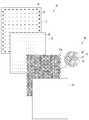
도 1a는 본 발명의 실시예에 의한 감지패턴들의 배치를 나타낸 평면도이고, 도 1b는 도 1a의 특정 부분(A-A')에 대한 단면도이다.FIG. 1A is a plan view illustrating an arrangement of sensing patterns according to an exemplary embodiment of the present invention, and FIG. 1B is a cross-sectional view of a specific portion A-A 'of FIG. 1A.
도 1a 및 도 1b를 참조하면, 본 발명의 실시예에 의한 감지패턴들은, 서로 교호적으로 배치되며 X 좌표가 동일한 하나의 열 또는 Y 좌표가 동일한 하나의 행 단위로 서로 연결되도록 형성된 제1 및 제2 감지패턴들(12, 14)을 포함한다.1A and 1B, the sensing patterns according to an embodiment of the present invention may be arranged alternately with each other and formed to be connected to each other in one row unit having the same X coordinate or the same Y coordinate in one row unit.
즉, 제1 감지패턴들(12)은 제1 방향(열 방향)을 따라 X 좌표가 동일한 하나의 열에 배치된 제1 감지셀(12') 및 인접한 상기 제1 감지셀(12')을 연결하는 제1 연결라인(12")으로 구성되고, 제2 감지패턴들(14)은 제2 방향(행 방향)을 따라 Y 좌표가 동일한 하나의 행에 배치된 제2 감지셀(14)로 구성된다.That is, the
이 때, 본 발명의 실시예의 경우 상기 제1 감지패턴들(12) 및 제2 감지패턴들(14)은 동일 레이어(layer)에 형성되고, 상기 제1 및 제2 감지패턴들(12, 14)는 터치 스크린 패널의 동작 구현을 위해 투명 재질로 구현되어야 하며, 이에 상기 제1 및 제2 감지패턴들(12, 14)은 인듐-틴 옥사이드(이하, ITO)로 구현됨이 바람직하다.In this case, in the embodiment of the present invention, the
또한, 상기 제1 감지패턴들(12) 및 제2 감지패턴들(14)이 감지 전극으로서의 역할을 수행하기 위해서는 제 1방향 및 제2방향으로 배열된 각각의 감지셀들이 전기적으로 연결되어야 한다.In addition, in order for the
이에 상기 제1 감지셀(12')들은 제1 연결라인(12")에 의해 서로 전기적으로 연결되나, 상기 제2 감지패턴들을 구성하는 제2 감지셀(14)들은 상기 제1 감지셀(12')과 동일 레이어에 형성되기 때문에 상기 제1 연결라인(12')와 단락을 피하기 위해 상기 제1 연결라인과 교차되는 연결라인이 동일 레이어 상에는 형성될 수 없다.Accordingly, the
이에 본 발명은 상기 각각의 제2 감지셀(14)을 전기적으로 연결하는 각각의 연결패턴(15')이 제1 감지패턴들(12)과는 다른 레이어에 형성되는 것으로, 제1 및 제2 감지패턴들(12, 14)의 하부 레이어에 형성됨을 특징으로 한다.Accordingly, in the present invention, each
즉, 본 발명의 실시예는 투명 기판(11) 상에 연결패턴(15')들이 형성되고, 상기 연결패턴(15')를 포함한 투명기판(11) 상에 절연막(13)이 형성된다.That is, in the embodiment of the present invention, the connection patterns 15 'are formed on the
이 때, 상기 연결패턴(15')들은 제1 및 제2 감지패턴들(12, 14)과 같은 ITO로 형성되거나, 상기 ITO보다 낮은 저항값을 갖는 금속 물질로 형성될 수 있다.In this case, the
또한, 상기 연결패턴(15')은 도시된 바와 같이 직사각형 바(bar) 형태로 이루어질 수 있으나, 이는 하나의 실시예로서 반드시 이러한 형상에 한정되지 않는다. 즉, 상기 절연막(13)의 콘택홀(13')에 의해 노출되는 부분인 연결패턴(15')의 끝단부의 폭이 상기 연결패턴(15')의 타 부위의 폭보다 넓은 형상으로 구현될 수도 있다.In addition, the
이와 같은 연결패턴(15')은 상기 제1 감지패턴들(12)의 제1 연결라인(12")과 서로 교차되는데, 상기 교차에 의해 발생되는 기생 캐패시턴스의 영향을 줄이기 위해 상기 연결패턴(15')의 폭을 최소화하는 것이 바람직하다.The
그러나, 이와 같이 상기 연결패턴(15')의 폭을 최소화할 경우 각각 제2 감지패턴들(14)의 라인 저항이 높아져 결과적으로 터치 스크린 패널의 기능을 구현하는 센싱 감도가 저하되는 문제가 발생한다.However, when the width of the connection pattern 15 'is minimized, the line resistance of each of the
이에 상기 연결패턴(15')은 저항이 낮은 도전성 물질로 형성함이 보다 바람직하다.Accordingly, the
이 경우, 상기 연결패턴(15')은 상기 제1 감지패턴들(12) 및 제2 감지패턴들(14)이 형성되는 영역의 가장자리 영역에 형성되어 감지된 신호를 구동회로(미도시) 측으로 공급하는 금속패턴(미도시)과 동일한 재질로 형성되는 것으로, 상기 금속패턴과 동일한 레이어에 동일 공정을 통해 형성되므로 상기 연결패턴(15')을 형성하기 위해 추가의 마스크 공정이 필요하지 않는다.In this case, the
따라서, 상기 연결패턴(15')을 상기 제1 및 제2 감지패턴들(12, 14)과 같은 투명 도전성 물질 물질로 형성하지 않아, 라인 저항이 높아짐을 방지함과 아울러 상기 연결패턴(15')을 형성하기 위해 마스크 공정이 추가되어야 하는 단점도 극복할 수 있음을 그 특징으로 한다.Therefore, the
도 2는 본 발명의 실시예에 의한 터치 스크린 패널의 분해평면도이다.2 is an exploded plan view of a touch screen panel according to an exemplary embodiment of the present invention.
단, 도 2에 도시된 실시예에서는 연결패턴(15')이 ITO가 아닌 저 저항의 도전성 물질로 구현됨을 그 예로 설명하도록 한다.However, in the embodiment shown in FIG. 2, the
도 2를 참조하면, 본 발명의 실시예에 의한 터치 스크린 패널(10)은, 투명기판(11)과; 상기 투명기판(11) 상에 아일랜드 형태로 다수 배열되도록 형성된 연결패턴(15')들과; 상기 연결패턴(15')들 상에 형성되며, 각 연결패턴(15')의 끝단부에 대응되는 영역에 각각 콘택홀(13')들이 형성된 제1 절연막(13)과; 상기 제1 절연막(13) 상에 형성된 제1 및 제2 감지패턴들(12, 14)이 포함된다.2, the
이 때, 상기 제2 감지패턴을 구성하는 제2 감지셀(14)들은 상기 인접한 한 쌍의 콘택홀(13')을 포함하는 영역 상에 각각 형성되며, 이에 따라 상기 콘택 홀(13')을 통해 노출된 연결패턴(15')들과 전기적으로 연결됨을 특징으로 한다.In this case, the
또한, 상기 제1 및 제2 감지패턴들(12, 14)이 형성되는 영역의 가장자리에 배치되어 상기 하나의 열 또는 행 단위의 감지패턴들을 위치 검출라인과 전기적으로 연결하는 다수의 금속패턴들(15)이 더 포함되어 구성된다.In addition, a plurality of metal patterns disposed on an edge of a region where the first and
즉, 상기 금속패턴들(15)은 제1 및 제2 감지패턴들(12, 14)이 형성되는 영역의 가장자리 영역, 특히, 제1 및 제2 감지패턴들(12, 14)의 패드(12a, 14a)와 대응되는 영역에 배치된다. 이와 같은 금속패턴들(15)은 하나의 열 또는 행 단위의 감지패턴들(12, 14)을 각각 위치 검출라인(미도시)과 전기적으로 연결하여 도시되지 않은 구동회로 등으로 접촉위치 검출신호가 공급되도록 한다.That is, the
상기 다수의 금속패턴들(15)은 상기 연결패턴들(15')와 동일 공정을 통해 형성됨이 바람직하며, 이에 따라 상기 금속패턴들(15)은 상기 투명기판(11) 상에 형성되며, 저 저항의 도전성 물질로 구현된다.The plurality of
제1 감지패턴들(12)은 제1 절연막(13)의 일면 상에 제1 방향을 따라 연결되도록 형성된다. 예컨대, 제1 감지패턴들(12)은 제1 절연막(13)의 상부면 상에 다이아몬드 패턴과 같이 규칙적인 패턴을 갖는 제1 감지셀들(12')로 밀접되도록 형성될 수 있다.The
즉, 상기 제1 감지패턴들(12)은 제1 방향(열 방향)을 따라 X 좌표가 동일한 하나의 열에 배치된 제1 감지셀(12') 및 인접한 상기 제1 감지셀(12')을 연결하는 제1 연결라인(12")으로 구성된다. 여기서, 제1 감지셀들(12')의 형상은 다이아몬드 형상에 한정되는 것은 아니며, 제1 감지셀들(12')이 밀접될 수 있는 다양한 형상으 로 구현될 수 있다.That is, the
그리고, 제1 감지패턴들(12)은 열 단위로 상기 금속패턴들(15)과 전기적으로 연결될 수 있도록 패드(12a)를 구비한다. 제1 감지패턴들(12)의 패드(12a)는 열 단위로 상, 하측에 교번적으로 구비되거나, 혹은 상, 하측 모두에 구비될 수 있다.The
또한, 상기 제2 감지패턴들(14)은 상기 제1 감지패턴들(12)이 형성된 제1 절연막(13) 상에 제2 방향을 따라 형성되되, 제1 감지패턴들(12)과 중첩되지 않도록 상기 제1 감지패턴들(12)과 교호적으로 배치된다.In addition, the
즉, 상기 제2 감지패턴들은 제2 방향(행 방향)을 따라 Y 좌표가 동일한 하나의 열에 배치된 제2 감지셀(14)들로 구성되는 것으로, 상기 제2 감지셀들(14)은 제1 감지셀들(12')과 동일한 다이아몬드 패턴으로 밀접되도록 형성된다.That is, the second sensing patterns are composed of
그리고, 제2 감지패턴들(14)은 행 단위로 금속패턴들(15)과 전기적으로 연결될 수 있도록 패드(14a)를 구비한다. 제2 감지패턴들(14)의 패드(14a)는 행 단위로 좌, 우측에 교번적으로 구비되거나, 혹은 좌, 우측 모두에 구비될 수 있다.In addition, the
이 때, 상기 제1 감지셀들(12')은 제2 감지셀들(14)과 중첩되는 영역에는 형성되지 않는다. 즉, 상기 제1 감지셀들(12')과 제2 감지셀들(14)은 서로 어긋나도록 교호적으로 배치된다.In this case, the
단, 상기 제2 감지셀들(14)은 상기 제1 절연막(13) 상에 형성됨에 있어서, 상기 제1 절연막(13)에 구비된 인접한 한 쌍의 콘택홀(13')을 포함하는 영역 상에 각각 형성됨을 특징으로 하는 것으로, 상기 콘택홀(13')들을 통해 노출된 연결패턴(15')들과 전기적으로 연결된다.However, when the
이와 같은 본 발명의 실시예에 의하면 상기 연결패턴(15')이 터치 스크린 패널(10)의 가장 아래 레이어에 형성됨으로써, 외부에서 입력되는 정전기에 대한 취약성을 개선할 수 있으며, 상기 제1 절연막(13)과의 밀착 안정성을 확보할 수 있게 된다.According to the exemplary embodiment of the present invention, since the
한편, 제1 및 제2 감지패턴들(12, 14)과 제1 절연막(13)은 터치 스크린 패널(10)의 하부에 배치되는 표시패널(미도시) 등에서 방출되는 빛이 터치 스크린 패널(10)을 투과할 수 있도록 투명물질로 형성된다. 즉, 제1 및 제2 감지패턴들(12, 14)은 인듐-틴 옥사이드(이하, ITO)와 같은 투명 전극물질로 형성되고, 제1 절연막(13)은 투명 절연물질로 형성된다.The first and
그리고, 이들의 두께는 표시패널로부터의 빛이 투과되는 투과율을 확보하면서도 터치 스크린 패널(10)(특히, 제1 및 제2 감지패턴들(12, 14))이 비교적 낮은 면저항을 가질 수 있는 범위 내에서 설정될 수 있다. 즉, 제1 및 제2 감지패턴들(12, 14)과 제1 절연막(13)의 두께는 투과율과 면저항을 고려하여 최적화되도록 설정될 수 있다.In addition, the thickness of the touch screen panel 10 (particularly, the first and
예를 들어, 제1 및 제2 감지패턴들(12, 14)은 각각 100 내지 300 Å 두께의 인듐-틴 옥사이드(이하, ITO) 패턴으로 형성되고, 제1 절연막(13)은 1.6~1.9의 광굴절률이 확보되는 400 내지 1000 Å 두께(특히 400 내지 700 Å 두께)의 투명 절연물질로 형성될 수 있다. 단, 이는 단지 하나의 실시예로 본 발명이 이에 한정되는 것은 아니며, 이들의 두께는 투과율 및/또는 면저항 등을 고려하여 변경될 수 있음은 물론이다.For example, the first and
또한, 제2 절연막(16)은 상기 제1 및 제2 감지패턴들(12, 14) 상에 이들을 커버하도록 형성된다. 예를 들어, 제2 절연막(16)은 제1 및 제2 감지패턴들(12, 14) 상에 400 내지 1000 Å 두께의 투명 절연물질로 형성될 수 있다. 단, 상기 제2 절연막(16)은 제품 설계에 따라 생략될 수도 있다.In addition, the second insulating
전술한 바와 같은 터치 스크린 패널(10)은 사람의 손 또는 물체가 터치 스크린 패널(10)에 접촉되면, 제1 및 제2 감지패턴들(12, 14), 금속패턴들(15) 및 위치 검출라인을 경유하여 구동회로 측으로 접촉위치에 따른 정전용량의 변화가 전달된다. 그리고, X 및 Y 입력처리회로(미도시) 등에 의해 정전용량의 변화가 전기적 신호로 변환됨에 의해 접촉위치가 파악된다.As described above, the
한편, 연결패턴(15')이 형성된 투명기판(11)의 일면과 반대되는 타측면, 예컨대, 투명기판(11)의 하부면에는 투명 접지전극(미도시)과, 투명 접지전극을 커버하는 제3 절연막(미도시)이 더 형성될 수 있다.Meanwhile, a transparent ground electrode (not shown) and a transparent ground electrode are formed on the other side surface opposite to one surface of the
예를 들어, 투명기판(11)의 하부면에는 100 내지 300 Å 두께를 갖는 ITO 등의 투명 전극물질로 형성된 투명 접지전극이 형성되고, 투명 접지전극의 하부에는 이를 커버하는 400 내지 1000 Å 두께의 제3 절연막이 형성될 수 있다.For example, a transparent ground electrode formed of a transparent electrode material such as ITO having a thickness of 100 to 300 m 3 is formed on a lower surface of the
하지만, 이는 단지 하나의 실시예로 투명 접지전극 및 제3 절연막의 두께 등은 광투과율 등을 고려하여 변형 실시될 수 있다. 또한, 투명 접지전극 및/또는 제3 절연막은 제품 설계에 따라 생략되는 것도 가능하다.However, in one embodiment, the thicknesses of the transparent ground electrode and the third insulating layer may be modified in consideration of light transmittance. In addition, the transparent ground electrode and / or the third insulating film may be omitted depending on the product design.
투명 접지전극은 터치 스크린 패널(10)과 표시패널 등의 사이에서 안정성을 확보하는데 이용될 수 있고, 터치 스크린 패널(10)의 설계 방식에 따라서는 제1 및 제2 감지패턴들(12, 14)과 정전용량을 형성하는 데에도 이용될 수 있다.The transparent ground electrode may be used to secure stability between the
즉, 정전용량의 터치 스크린 패널(10)에서, 접촉위치를 감지하기 위해 제1 감지패턴(12)과 제2 감지패턴(14) 사이의 정전용량이 이용되거나, 혹은 제1 및 제2 감지패턴(12, 14)과 투명 접지전극 사이의 정전용량이 이용될 수 있는 것으로, 이는 다양하게 변형 실시가 가능하다.That is, in the capacitive
본 발명의 기술 사상은 상기 바람직한 실시예에 따라 구체적으로 기술되었으나, 상기한 실시예는 그 설명을 위한 것이며 그 제한을 위한 것이 아님을 주의하여야 한다. 또한, 본 발명의 기술 분야의 통상의 지식을 가진 자라면 본 발명의 기술 사상의 범위 내에서 다양한 변형예가 가능함을 이해할 수 있을 것이다.While the present invention has been particularly shown and described with reference to exemplary embodiments thereof, it is to be understood that the invention is not limited to the disclosed exemplary embodiments. It will be apparent to those skilled in the art that various modifications may be made without departing from the scope of the present invention.
도 1a는 본 발명의 실시예에 의한 감지패턴들의 배치를 나타낸 평면도.1A is a plan view showing the arrangement of sensing patterns according to an embodiment of the present invention.
도 1b는 도 1a의 특정 부분(A-A')에 대한 단면도.FIG. 1B is a cross-sectional view of a particular portion A-A 'of FIG. 1A. FIG.
도 2는 본 발명의 실시예에 의한 터치 스크린 패널의 분해평면도.2 is an exploded plan view of a touch screen panel according to an exemplary embodiment of the present invention.
<도면의 주요 부분에 대한 부호의 설명><Explanation of symbols for the main parts of the drawings>
12: 제1 감지패턴12': 제1 감지셀12: first sensing pattern 12 ': first sensing cell
12": 제1 연결라인14: 제2 감지패턴(제2 감지셀)12 ": first connection line 14: second sensing pattern (second sensing cell)
13: 절연막(제1 절연막)13': 콘택홀13: insulating film (first insulating film) 13 ': contact hole
15: 금속패턴15': 연결패턴15: metal pattern 15 ': connection pattern
Claims (9)
Translated fromKoreanPriority Applications (2)
| Application Number | Priority Date | Filing Date | Title |
|---|---|---|---|
| KR1020090003644AKR101022087B1 (en) | 2009-01-16 | 2009-01-16 | Touch screen panel |
| US12/591,159US8358284B2 (en) | 2009-01-16 | 2009-11-10 | Touch screen panel |
Applications Claiming Priority (1)
| Application Number | Priority Date | Filing Date | Title |
|---|---|---|---|
| KR1020090003644AKR101022087B1 (en) | 2009-01-16 | 2009-01-16 | Touch screen panel |
Publications (2)
| Publication Number | Publication Date |
|---|---|
| KR20100084263A KR20100084263A (en) | 2010-07-26 |
| KR101022087B1true KR101022087B1 (en) | 2011-03-17 |
Family
ID=42336556
Family Applications (1)
| Application Number | Title | Priority Date | Filing Date |
|---|---|---|---|
| KR1020090003644AActiveKR101022087B1 (en) | 2009-01-16 | 2009-01-16 | Touch screen panel |
Country Status (2)
| Country | Link |
|---|---|
| US (1) | US8358284B2 (en) |
| KR (1) | KR101022087B1 (en) |
Cited By (3)
| Publication number | Priority date | Publication date | Assignee | Title |
|---|---|---|---|---|
| US9244486B2 (en) | 2012-09-11 | 2016-01-26 | Samsung Display Co., Ltd. | Flexible touch screen panel |
| US9582087B2 (en) | 2012-11-23 | 2017-02-28 | Samsung Display Co., Ltd. | Flexible touch screen panel and method of manufacturing the same |
| KR20220135633A (en) | 2021-03-31 | 2022-10-07 | 동우 화인켐 주식회사 | Touch screen panel and method for the same |
Families Citing this family (30)
| Publication number | Priority date | Publication date | Assignee | Title |
|---|---|---|---|---|
| KR101073333B1 (en) | 2009-08-27 | 2011-10-12 | 삼성모바일디스플레이주식회사 | Touch Screen Panel and fabrication method thereof |
| TWI396901B (en)* | 2009-12-21 | 2013-05-21 | Au Optronics Corp | Method of fabricating touch panel |
| KR101040846B1 (en)* | 2010-03-16 | 2011-06-14 | 삼성모바일디스플레이주식회사 | Touch screen panel and its manufacturing method |
| KR101082219B1 (en) | 2010-03-16 | 2011-11-09 | 삼성모바일디스플레이주식회사 | plat panel display integrated with Touch Screen Panel |
| KR101100987B1 (en) | 2010-03-23 | 2011-12-30 | 삼성모바일디스플레이주식회사 | Touch screen panel |
| US8800026B2 (en)* | 2010-06-18 | 2014-08-05 | Sharp Kabushiki Kaisha | Information terminal device and method of personal authentication using the same |
| CN102314271B (en)* | 2010-07-07 | 2014-11-05 | 宸鸿科技(厦门)有限公司 | Capacitive touch graphic structure and manufacturing method thereof, touch panel and touch display device |
| KR101710552B1 (en)* | 2010-07-20 | 2017-02-28 | 삼성디스플레이 주식회사 | Touch screen panel |
| WO2012047014A2 (en)* | 2010-10-05 | 2012-04-12 | 네오뷰코오롱 주식회사 | Electrostatic capacity-type touch panel device and method for manufacturing same |
| WO2012047013A2 (en)* | 2010-10-05 | 2012-04-12 | 네오뷰코오롱 주식회사 | Electrostatic capacity-type touch panel device and method for manufacturing same |
| CN101976146B (en)* | 2010-10-12 | 2012-05-30 | 友达光电股份有限公司 | Manufacturing method of touch panel |
| KR101448251B1 (en)* | 2010-10-28 | 2014-10-08 | 삼성디스플레이 주식회사 | Touch Screen Panel and Display Device Having the Same |
| JP5755752B2 (en)* | 2010-11-09 | 2015-07-29 | ティーピーケイ タッチ ソリューションズ インコーポレーテッド | Touch panel device |
| US9652089B2 (en)* | 2010-11-09 | 2017-05-16 | Tpk Touch Solutions Inc. | Touch panel stackup |
| KR101328832B1 (en) | 2011-03-14 | 2013-11-13 | 삼성전자주식회사 | Touch panel and touch screen having the same |
| KR101311750B1 (en)* | 2011-05-09 | 2013-09-26 | 주식회사 상보 | Carbon nanotube based touch panel |
| KR101283511B1 (en)* | 2011-08-30 | 2013-07-15 | 위스트론 코포레이션 | Seamless capacitive touch panel |
| US9170695B2 (en) | 2011-09-01 | 2015-10-27 | Wistron Corporation | Seamless capacitive touch panel |
| US8680419B2 (en) | 2011-09-01 | 2014-03-25 | Wistron Corporation | Seamless capacitive touch panel |
| CN102981664B (en)* | 2011-09-07 | 2016-10-05 | 宸鸿科技(厦门)有限公司 | Touch electrode structure and the contact panel of application thereof |
| KR101987338B1 (en)* | 2011-12-16 | 2019-06-11 | 엘지이노텍 주식회사 | Touch window |
| KR101976089B1 (en)* | 2012-08-27 | 2019-05-10 | 삼성디스플레이 주식회사 | Touch Screen Panel |
| CN104007864B (en)* | 2013-02-27 | 2017-09-12 | 宸鸿科技(厦门)有限公司 | Contact panel and preparation method thereof |
| WO2015037898A1 (en)* | 2013-09-10 | 2015-03-19 | 미래나노텍 주식회사 | Capacitive-type touch screen sensor, touch screen panel and image display device |
| KR20150029507A (en) | 2013-09-10 | 2015-03-18 | 미래나노텍(주) | Touch screen sensor, Touch screen panel of electrostatic capacitive type and image display device |
| KR102294702B1 (en) | 2014-06-03 | 2021-08-26 | 동우 화인켐 주식회사 | Touch screen panel |
| KR102301502B1 (en) | 2015-01-07 | 2021-09-24 | 삼성디스플레이 주식회사 | Touch screen panel comprising touch sensor |
| KR20180095174A (en)* | 2017-02-17 | 2018-08-27 | 동우 화인켐 주식회사 | Digitizer and Flexible Display Comprising the Same |
| KR102311316B1 (en) | 2017-04-24 | 2021-10-13 | 삼성디스플레이 주식회사 | Display device and fabricating method of the same |
| CN109634457A (en)* | 2018-12-03 | 2019-04-16 | 武汉华星光电半导体显示技术有限公司 | Touch control electrode and touch control display apparatus |
Citations (2)
| Publication number | Priority date | Publication date | Assignee | Title |
|---|---|---|---|---|
| KR20080049248A (en)* | 2006-11-30 | 2008-06-04 | 엘지디스플레이 주식회사 | Display device |
| KR20080110477A (en)* | 2007-06-14 | 2008-12-18 | 엡슨 이미징 디바이스 가부시키가이샤 | Capacitive input device |
Family Cites Families (14)
| Publication number | Priority date | Publication date | Assignee | Title |
|---|---|---|---|---|
| DE69324067T2 (en) | 1992-06-08 | 1999-07-15 | Synaptics Inc | Object position detector |
| WO2000054307A1 (en)* | 1999-03-05 | 2000-09-14 | Canon Kabushiki Kaisha | Image forming device |
| KR100654956B1 (en) | 2000-12-30 | 2006-12-07 | 현대엘씨디주식회사 | Organic electroluminescent liquid crystal display device |
| FR2823010B1 (en)* | 2001-04-02 | 2003-08-15 | St Microelectronics Sa | METHOD FOR MANUFACTURING A VERTICAL TRANSISTOR WITH AN INSULATED GRID WITH A QUADRUPLE CONDUCTION CHANNEL, AND INTEGRATED CIRCUIT COMPRISING SUCH A TRANSISTOR |
| KR20030061070A (en) | 2002-01-10 | 2003-07-18 | 주식회사 에이터치 | Structure of Electrodes in Touch Screen |
| JP2003288166A (en) | 2002-03-27 | 2003-10-10 | Fujitsu Component Ltd | Connection structure between touch panel and external lead wire |
| KR100510721B1 (en) | 2002-11-14 | 2005-08-30 | 엘지.필립스 엘시디 주식회사 | touch panel for display device |
| US6970160B2 (en)* | 2002-12-19 | 2005-11-29 | 3M Innovative Properties Company | Lattice touch-sensing system |
| US20050084659A1 (en)* | 2003-10-20 | 2005-04-21 | General Atomics | Vehicle windshield head-up display |
| US7339579B2 (en) | 2003-12-15 | 2008-03-04 | 3M Innovative Properties Company | Wiring harness and touch sensor incorporating same |
| US8004504B2 (en)* | 2004-09-27 | 2011-08-23 | Qualcomm Mems Technologies, Inc. | Reduced capacitance display element |
| KR20080047902A (en)* | 2006-11-27 | 2008-05-30 | 삼성전자주식회사 | Touch sensor |
| TW200842681A (en)* | 2007-04-27 | 2008-11-01 | Tpk Touch Solutions Inc | Touch pattern structure of a capacitive touch panel |
| TW200844827A (en)* | 2007-05-11 | 2008-11-16 | Sense Pad Tech Co Ltd | Transparent touch panel device |
- 2009
- 2009-01-16KRKR1020090003644Apatent/KR101022087B1/enactiveActive
- 2009-11-10USUS12/591,159patent/US8358284B2/enactiveActive
Patent Citations (2)
| Publication number | Priority date | Publication date | Assignee | Title |
|---|---|---|---|---|
| KR20080049248A (en)* | 2006-11-30 | 2008-06-04 | 엘지디스플레이 주식회사 | Display device |
| KR20080110477A (en)* | 2007-06-14 | 2008-12-18 | 엡슨 이미징 디바이스 가부시키가이샤 | Capacitive input device |
Cited By (3)
| Publication number | Priority date | Publication date | Assignee | Title |
|---|---|---|---|---|
| US9244486B2 (en) | 2012-09-11 | 2016-01-26 | Samsung Display Co., Ltd. | Flexible touch screen panel |
| US9582087B2 (en) | 2012-11-23 | 2017-02-28 | Samsung Display Co., Ltd. | Flexible touch screen panel and method of manufacturing the same |
| KR20220135633A (en) | 2021-03-31 | 2022-10-07 | 동우 화인켐 주식회사 | Touch screen panel and method for the same |
Also Published As
| Publication number | Publication date |
|---|---|
| KR20100084263A (en) | 2010-07-26 |
| US20100182256A1 (en) | 2010-07-22 |
| US8358284B2 (en) | 2013-01-22 |
Similar Documents
| Publication | Publication Date | Title |
|---|---|---|
| KR101022087B1 (en) | Touch screen panel | |
| KR101073285B1 (en) | Touch Screen Panel | |
| KR101022185B1 (en) | Touch screen panel | |
| US11106322B2 (en) | Touch screen panel | |
| KR101022105B1 (en) | Touch screen panel and its manufacturing method | |
| KR101040881B1 (en) | Touch screen panel | |
| KR101073333B1 (en) | Touch Screen Panel and fabrication method thereof | |
| KR101040846B1 (en) | Touch screen panel and its manufacturing method | |
| KR101101088B1 (en) | Touch screen panel and its manufacturing method | |
| KR101048930B1 (en) | Touch screen panel | |
| KR101976089B1 (en) | Touch Screen Panel | |
| KR101975535B1 (en) | flexible touch screen panel | |
| KR20100006987A (en) | Touch screen panel and fabricating method for the same | |
| US20110248938A1 (en) | Touch screen panel | |
| JP2011086149A (en) | Capacitive touch sensor | |
| KR101048913B1 (en) | Touch screen panel | |
| KR101056264B1 (en) | Touch screen panel | |
| KR101073161B1 (en) | Touch screen panel | |
| KR20140054756A (en) | Touch screen panel |
Legal Events
| Date | Code | Title | Description |
|---|---|---|---|
| A201 | Request for examination | ||
| PA0109 | Patent application | Patent event code:PA01091R01D Comment text:Patent Application Patent event date:20090116 | |
| PA0201 | Request for examination | ||
| PG1501 | Laying open of application | ||
| E902 | Notification of reason for refusal | ||
| PE0902 | Notice of grounds for rejection | Comment text:Notification of reason for refusal Patent event date:20100831 Patent event code:PE09021S01D | |
| E701 | Decision to grant or registration of patent right | ||
| PE0701 | Decision of registration | Patent event code:PE07011S01D Comment text:Decision to Grant Registration Patent event date:20110226 | |
| GRNT | Written decision to grant | ||
| PR0701 | Registration of establishment | Comment text:Registration of Establishment Patent event date:20110307 Patent event code:PR07011E01D | |
| PR1002 | Payment of registration fee | Payment date:20110307 End annual number:3 Start annual number:1 | |
| PG1601 | Publication of registration | ||
| FPAY | Annual fee payment | Payment date:20140303 Year of fee payment:4 | |
| PR1001 | Payment of annual fee | Payment date:20140303 Start annual number:4 End annual number:4 | |
| FPAY | Annual fee payment | Payment date:20150227 Year of fee payment:5 | |
| PR1001 | Payment of annual fee | Payment date:20150227 Start annual number:5 End annual number:5 | |
| FPAY | Annual fee payment | Payment date:20180302 Year of fee payment:8 | |
| PR1001 | Payment of annual fee | Payment date:20180302 Start annual number:8 End annual number:8 | |
| FPAY | Annual fee payment | Payment date:20190304 Year of fee payment:9 | |
| PR1001 | Payment of annual fee | Payment date:20190304 Start annual number:9 End annual number:9 | |
| FPAY | Annual fee payment | Payment date:20200227 Year of fee payment:10 | |
| PR1001 | Payment of annual fee | Payment date:20200227 Start annual number:10 End annual number:10 | |
| PR1001 | Payment of annual fee | Payment date:20210302 Start annual number:11 End annual number:11 | |
| PR1001 | Payment of annual fee | Payment date:20220302 Start annual number:12 End annual number:12 | |
| PR1001 | Payment of annual fee | Payment date:20250224 Start annual number:15 End annual number:15 |