KR101021552B1 - EMI noise reduction printed circuit board - Google Patents
EMI noise reduction printed circuit boardDownload PDFInfo
- Publication number
- KR101021552B1 KR101021552B1KR1020090089666AKR20090089666AKR101021552B1KR 101021552 B1KR101021552 B1KR 101021552B1KR 1020090089666 AKR1020090089666 AKR 1020090089666AKR 20090089666 AKR20090089666 AKR 20090089666AKR 101021552 B1KR101021552 B1KR 101021552B1
- Authority
- KR
- South Korea
- Prior art keywords
- region
- conductive plate
- printed circuit
- circuit board
- noise
- Prior art date
- Legal status (The legal status is an assumption and is not a legal conclusion. Google has not performed a legal analysis and makes no representation as to the accuracy of the status listed.)
- Expired - Fee Related
Links
Images


Classifications
- H—ELECTRICITY
- H05—ELECTRIC TECHNIQUES NOT OTHERWISE PROVIDED FOR
- H05K—PRINTED CIRCUITS; CASINGS OR CONSTRUCTIONAL DETAILS OF ELECTRIC APPARATUS; MANUFACTURE OF ASSEMBLAGES OF ELECTRICAL COMPONENTS
- H05K1/00—Printed circuits
- H05K1/02—Details
- H05K1/0213—Electrical arrangements not otherwise provided for
- H05K1/0216—Reduction of cross-talk, noise or electromagnetic interference
- H05K1/0236—Electromagnetic band-gap structures
- H—ELECTRICITY
- H05—ELECTRIC TECHNIQUES NOT OTHERWISE PROVIDED FOR
- H05K—PRINTED CIRCUITS; CASINGS OR CONSTRUCTIONAL DETAILS OF ELECTRIC APPARATUS; MANUFACTURE OF ASSEMBLAGES OF ELECTRICAL COMPONENTS
- H05K1/00—Printed circuits
- H05K1/02—Details
- H—ELECTRICITY
- H05—ELECTRIC TECHNIQUES NOT OTHERWISE PROVIDED FOR
- H05K—PRINTED CIRCUITS; CASINGS OR CONSTRUCTIONAL DETAILS OF ELECTRIC APPARATUS; MANUFACTURE OF ASSEMBLAGES OF ELECTRICAL COMPONENTS
- H05K3/00—Apparatus or processes for manufacturing printed circuits
- H05K3/46—Manufacturing multilayer circuits
- H—ELECTRICITY
- H05—ELECTRIC TECHNIQUES NOT OTHERWISE PROVIDED FOR
- H05K—PRINTED CIRCUITS; CASINGS OR CONSTRUCTIONAL DETAILS OF ELECTRIC APPARATUS; MANUFACTURE OF ASSEMBLAGES OF ELECTRICAL COMPONENTS
- H05K9/00—Screening of apparatus or components against electric or magnetic fields
- H—ELECTRICITY
- H05—ELECTRIC TECHNIQUES NOT OTHERWISE PROVIDED FOR
- H05K—PRINTED CIRCUITS; CASINGS OR CONSTRUCTIONAL DETAILS OF ELECTRIC APPARATUS; MANUFACTURE OF ASSEMBLAGES OF ELECTRICAL COMPONENTS
- H05K2201/00—Indexing scheme relating to printed circuits covered by H05K1/00
- H05K2201/09—Shape and layout
- H05K2201/09209—Shape and layout details of conductors
- H05K2201/0929—Conductive planes
- H05K2201/09309—Core having two or more power planes; Capacitive laminate of two power planes
- H—ELECTRICITY
- H05—ELECTRIC TECHNIQUES NOT OTHERWISE PROVIDED FOR
- H05K—PRINTED CIRCUITS; CASINGS OR CONSTRUCTIONAL DETAILS OF ELECTRIC APPARATUS; MANUFACTURE OF ASSEMBLAGES OF ELECTRICAL COMPONENTS
- H05K2201/00—Indexing scheme relating to printed circuits covered by H05K1/00
- H05K2201/09—Shape and layout
- H05K2201/09209—Shape and layout details of conductors
- H05K2201/095—Conductive through-holes or vias
- H05K2201/09627—Special connections between adjacent vias, not for grounding vias
Landscapes
- Engineering & Computer Science (AREA)
- Microelectronics & Electronic Packaging (AREA)
- Physics & Mathematics (AREA)
- Electromagnetism (AREA)
- Manufacturing & Machinery (AREA)
- Shielding Devices Or Components To Electric Or Magnetic Fields (AREA)
Abstract
Description
Translated fromKorean본 발명은 기판에 관한 것으로서, 보다 구체적으로는 전자기 밴드갭 구조(EBG structure)를 이용하여 전자기 간섭 노이즈(EMI noise)를 저감시킬 수 있는 노이즈 저감 기판에 관한 것이다.BACKGROUND OF THE INVENTION 1. Field of the Invention The present invention relates to a substrate, and more particularly, to a noise reduction substrate capable of reducing electromagnetic noise by using an electromagnetic bandgap structure (EBG structure).
EMI(Electromagnetic interference) 문제는 전자제품의 동작주파수가 고속화되면서 고질적인 노이즈 문제로 인식되어 왔다. 특히, 최근 들어 전자제품의 동작주파수가 수십 MHz ~ 수 GHz 대로 되면서 이러한 EMI 문제는 더더욱 심각해져서 해결책이 절실히 필요한 상황이다. 특히, 기판에서의 EMI 문제 중에서 기판 에지(edge)에서 발생하는 노이즈의 해결책에 대한 연구가 이루어지지 않아, 기판에서의 노이즈를 전면적으로 차단하는데 한계를 가지고 있다.Electromagnetic interference (EMI) problem has been recognized as a noise problem due to the high operating frequency of electronic products. In particular, as the operating frequency of electronic products has been in the range of several tens of MHz to several GHz, these EMI problems have become more serious and a solution is urgently needed. In particular, research on the solution of the noise generated at the substrate edge (edge) of the EMI problem in the substrate has not been made, there is a limit to block the noise in the substrate entirely.
EMI 노이즈는 어느 하나의 전자회로, 소자, 부품 등에서 발생한 전자기파(EM wave)가 다른 회로, 소자, 부품 등으로 전달됨으로써 간섭에 의한 노이즈 문제를 발생시키는 원인이 되는 노이즈를 말한다. 이와 같은 EMI 노이즈를 크게 분류하면, 방사 노이즈(radiation noise, 도 1의 참조번호 10, 30 참조)와 전도 노이즈(conduction noise, 도 1의 참조번호 20 참조)로 나눌 수 있다.EMI noise refers to noise that causes noise problems caused by interference by transmitting an electromagnetic wave generated in one electronic circuit, an element, or a component to another circuit, element, or component. If such EMI noise is largely classified, it can be divided into radiation noise (see
이 중, 기판의 상부(즉, 전자부품의 탑재면)로 방사되는 방사 노이즈(10)의 경우에는 메탈 캡 등의 전자기 차폐용 캡으로 기판 상부 영역을 쉴드(shield)함으로써 해결하는 방식이 일반적이지만, 기판 내부를 통해 흐르는 전도 노이즈(20)가 기판의 가장자리(edge)에까지 전도되어 기판 외부로 방사되는 방사 노이즈(30, 이하 이를 간단히 '에지 노이즈'라 칭함)에 대한 효과적인 해결책에 관한 연구는 아직 미흡한 단계이다.Among these, in the case of the
만일, 기판 구조의 간단한 변경만으로 기판 가장자리에서의 에지 노이즈를 저감할 수 있는 기술이 개발된다면, 메탈 캡이나 회로(circuit) 방식에 의한 해결 방법에 비해 개발 기간 및 비용을 획기적으로 줄일 수 있을 것으로 기대된다. 또한, 공간 활용 측면이나 소비 전력 측면에서도 이점을 가질 수 있으며, 손쉽게 수 GHz 이상의 대역에서도 노이즈를 제거할 수 있게 되어, 기판 에지에서의 EMI 노이즈 문제를 해결하는데 효과적일 것이다.If a technology is developed that can reduce edge noise at the edge of the substrate by simple modification of the substrate structure, it is expected that the development time and cost will be drastically reduced compared to the solution by the metal cap or circuit method. do. In addition, it can have advantages in terms of space utilization and power consumption, and can easily remove noise in a band of several GHz or more, thereby effectively solving the EMI noise problem at the substrate edge.
이에 따라, 본 발명은 특정 주파수 대역의 노이즈를 차폐할 수 있는 전자기 밴드갭 구조를 기판의 가장자리(edge)에 해당하는 기판 내부에 삽입시킴으로써, 기판 가장자리에서 방사되는 방사 노이즈(radiation noise)를 차폐시킬 수 있는 EMI 노이즈 저감 인쇄회로기판을 제공한다.Accordingly, the present invention inserts an electromagnetic bandgap structure that can shield noise of a specific frequency band into the substrate corresponding to the edge of the substrate, thereby shielding radiation noise emitted from the edge of the substrate. To provide EMI noise reduction printed circuit board.
또한, 본 발명은 기판의 간단한 구조 변경만으로 기판 가장자리에서 방사되는 방사 노이즈를 손쉽게 차폐 가능함으로써, 공간 활용도, 제조 비용, 소비 전력 등의 측면에서도 유리한 이점을 갖는 EMI 노이즈 저감 인쇄회로기판을 제공한다.In addition, the present invention provides an EMI noise reduction printed circuit board having advantageous advantages in terms of space utilization, manufacturing cost, power consumption, and the like, by easily shielding radiation noise emitted from the edge of the substrate only by changing the structure of the substrate.
본 발명의 이외의 목적들은 하기의 설명을 통해 쉽게 이해될 수 있을 것이다.Other objects of the present invention will be readily understood through the following description.
본 발명의 일 측면에 따르면, 노이즈 차폐를 위한 전자기 밴드갭 구조가 내부에 삽입되는 다층 인쇄회로기판으로서, 그라운드층과 전원층이 마련되는 제1 영역과; 상기 제1 영역의 측면에 위치하여, 상기 제1 영역의 측면을 통해 외부로 방사되는 EMI 노이즈를 차폐하도록 상기 전자기 밴드갭 구조가 마련되는 제2 영역을 포함하되, 상기 전자기 밴드갭 구조는, 상기 제1 영역의 측면을 따라 위치하는 복수 개의 제1 도전판과; 상기 제1 도전판과 다른 평면 상에, 상기 제1 도전판과 오버랩 되도록 배치되는 복수 개의 제2 도전판과; 상기 제1 도전판과 상기 제2 도전판을 연결하는 비아를 포함하는 것을 특징으로 하는 EMI 노이즈 저감 인쇄회로기판이 제공된다.According to an aspect of the present invention, a multilayer printed circuit board having an electromagnetic bandgap structure for noise shielding inserted therein, the first region having a ground layer and a power layer; A second region disposed on a side of the first region and provided with an electromagnetic bandgap structure to shield EMI noise radiated to the outside through the side of the first region, wherein the electromagnetic bandgap structure includes: A plurality of first conductive plates positioned along side surfaces of the first region; A plurality of second conductive plates disposed on a plane different from the first conductive plate so as to overlap the first conductive plate; An EMI noise reduction printed circuit board is provided, including vias connecting the first conductive plate and the second conductive plate.
상기 제1 영역과 상기 제2 영역은 4층 이상의 다층으로 이루어지고, 상기 비아는 상기 제2 영역의 상하를 관통하는 관통비아일 수 있다.The first region and the second region may be formed of a multilayer of four or more layers, and the via may be a through via penetrating the upper and lower portions of the second region.
또한, 상기 비아는 블라인드 비아일 수도 있다.The via may also be a blind via.
한편, 상기 제1 도전판과 상기 제2 도전판 중 적어도 어느 하나는, 상기 제1 영역의 가장자리 형상에 상응하여 절곡된 형상일 수도 있고, 상기 복수 개의 제1 도전판 중 서로 이웃하는 적어도 어느 한 쌍은, 연결라인에 의해 서로 전기적으로 연결될 수도 있다.Meanwhile, at least one of the first conductive plate and the second conductive plate may be bent to correspond to the edge shape of the first region, and at least one of the plurality of first conductive plates adjacent to each other. The pair may be electrically connected to each other by a connecting line.
상기 제1 도전판은 접속라인에 의해 상기 그라운드층과 전기적으로 연결될 수도 있으며, 상기 제2 영역은 상기 제1 영역의 측면 중 일부에만 선택적으로 배치될 수도 있다.The first conductive plate may be electrically connected to the ground layer by a connection line, and the second region may be selectively disposed only on a part of side surfaces of the first region.
본 발명의 바람직한 실시예에 따르면, 특정 주파수 대역의 노이즈를 차폐할 수 있는 전자기 밴드갭 구조를 기판의 가장자리(edge)에 해당하는 기판 내부에 삽입시킴으로써, 기판 가장자리에서 방사되는 방사 노이즈(radiation noise)를 차폐시킬 수 있는 효과가 있다.According to a preferred embodiment of the present invention, by inserting an electromagnetic bandgap structure capable of shielding noise of a specific frequency band into the substrate corresponding to the edge of the substrate, radiation noise radiated from the edge of the substrate There is an effect that can be shielded.
또한, 기판의 간단한 구조 변경만으로도 기판 가장자리에서 방사되는 방사 노이즈를 손쉽게 차폐 가능함으로써, 공간 활용도, 제조 비용, 소비 전력 등의 측면에서 유리한 효과가 있다.In addition, by simply changing the structure of the substrate can easily shield the radiation noise emitted from the edge of the substrate, there is an advantageous effect in terms of space utilization, manufacturing cost, power consumption.
본 발명은 다양한 변환을 가할 수 있고 여러 가지 실시예를 가질 수 있는 바, 특정 실시예들을 도면에 예시하고 상세한 설명에 상세하게 설명하고자 한다. 그러나, 이는 본 발명을 특정한 실시 형태에 대해 한정하려는 것이 아니며, 본 발명의 사상 및 기술 범위에 포함되는 모든 변환, 균등물 내지 대체물을 포함하는 것으로 이해되어야 한다.As the invention allows for various changes and numerous embodiments, particular embodiments will be illustrated in the drawings and described in detail in the written description. However, this is not intended to limit the present invention to specific embodiments, it should be understood to include all transformations, equivalents, and substitutes included in the spirit and scope of the present invention.
본 발명을 설명함에 있어서, 관련된 공지 기술에 대한 구체적인 설명이 본 발명의 요지를 불필요하게 흐릴 수 있다고 판단되는 경우 그 상세한 설명을 생략한다. 또한, 본 명세서의 설명 과정에서 이용되는 숫자(예를 들어, 제1, 제2 등)는 하나의 구성요소를 다른 구성요소와 구분하기 위한 식별기호에 불과하다.In describing the present invention, when it is determined that the detailed description of the related known technology may unnecessarily obscure the subject matter of the present invention, the detailed description thereof will be omitted. In addition, numerals (eg, first, second, etc.) used in the description process of the present specification are merely identification symbols for distinguishing one component from another component.
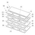
본 발명의 EMI 노이즈 저감 인쇄회로기판은 기판 내부의 전도 노이즈가 기판 에지 부분에까지 전도되어 기판 외부로 방사되는 것을 방지(즉, 에지 노이즈의 차폐)에 목적을 두고 있다. 이를 위해 본 실시예에 따른 인쇄회로기판은, 도 2 및 도 3에 도시된 바와 같이, 그라운드층(110)과 전원층(120)이 마련되는 제1 영역(100)과; 상기 제1 영역(100)의 측면에 위치하며 그 내부에 전자기 밴드갭 구조(이하 'EBG 구조')가 마련되는 제2 영역(200)을 포함한다. 이 때, EBG 구조는 상기 제1 영역(100)의 측면을 따라 위치하는 복수 개의 제1 도전판(210)과; 상기 제1 도전판(210)과 다른 평면 상에, 상기 제1 도전판(210)과 오버랩 되도록 배치되는 복수 개의 제2 도전판(220)과; 상기 제1 도전판(210)과 상기 제2 도전판(220)을 연결하는 비아(250, 250a)를 포함한다.The EMI noise reduction printed circuit board of the present invention aims to prevent conduction noise inside the substrate from being conducted to the edge of the substrate and radiating to the outside of the substrate (that is, shielding the edge noise). To this end, the printed circuit board according to the present exemplary embodiment includes a
상기와 같은 도전판들(210, 220)은 그 사이에 개재되는 유전체(105)와 더불어서 커패시턴스 성분을 구성하게 되고, 비아(250, 250a)는 인덕턴스 성분을 구성 하게 된다. 이러한 커패시턴스 성분과 인덕턴스 성분들의 조합에 의해 노이즈를 차폐하는 EBG 구조 즉, L-C 필터가 구성되는 것이다.The
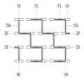
즉, 도 3에 도시된 바와 같이, 본 실시예에 따른 인쇄회로기판은 기판의 에지(edge) 부분에 도전판들(210, 220, 230, 240)을 형성하고, 이들을 서로 오버랩 되게 구성하여 비아(250, 250a)를 통해 연결함으로써, 기판의 에지부분에서 측면으로 방사되는 EMI 노이즈를 차폐하는 구조를 갖는다. 여기서 도전판들(210, 220, 230, 240)이 서로 오버랩 되기 때문에 상하층 간 커패시턴스 값을 향상시킬 수 있어 기판 에지로 전달되어 밖으로 방사되는 EMI 노이즈 차폐효과가 커질 수 있게 된다.That is, as illustrated in FIG. 3, the printed circuit board according to the present exemplary embodiment forms
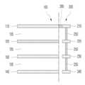
제1 영역(100)에는 그라운드층(110)과 전원층(120) 등과 같은 복수의 금속층(110, 120, 130, 140)이 마련된다. 도 3 및 도 5에는 최상층에 그라운드층(110)이 마련되고, 그 아래에 전원층(120)이 마련되는 구조가 제시되어 있다. 전원층(120) 아래에 마련되는 두 개의 금속층(130, 140)은 도 5에 도시된 바와 같이, 비아(150)에 의해 그라운드층(110)과 접지되는 구조를 갖을 수 있다. 전원층(120)에는 비아(150)와의 전기적인 분리를 위해 클리어런스 홀(125)이 형성된다. 각 층 사이에는 절연체(도 3의 105 참조) 또는 유전체가 개재된다.In the
그러나, 상기와 같은 제1 영역(100)의 구성은 일 예에 불과하며, 제1 영역(100)의 구조 및 배치가 다양하게 변경될 수도 있음은 물론이다.However, the configuration of the
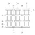
그라운드층(110)과 전원층(120)이 마련된 제1 영역(100)의 측면에 위치하는 제2 영역(200)에는, 도 4 및 도 5에 도시된 바와 같이, 복수의 도전판들(210, 220, 230, 240)이 서로 오버랩 되도록 배치된다. 보다 구체적으로, 복수 개의 제1 도전판들(210)이 제1 영역(100)의 측면을 따라 동일 평면 상에 배치되고, 제1 도전판들(210)과 다른 평면 상에 제2 도전판들(220)이 제1 영역(100)의 측면을 따라 배치된다. 이 때, 제2 도전판들(220)은 제1 도전판들(210)과 서로 대응되어 오버랩 되도록 배치된다. 이렇게 오버랩 된 제1 도전판(210)과 제2 도전판(220)의 소정의 위치는 비아(250)에 의해 서로 연결된다.As illustrated in FIGS. 4 and 5, the plurality of
여기서 제1 도전판과 제2 도전판은 특정한 기능을 수행하는 도전판을 지칭하는 것이 아니라, 서로 상이한 평면 상에 배치되는 도전판들(210, 220, 230, 240)을 서로 구분하기 위한 것에 지나지 않는다. 또한, 각각의 도전판들(210, 220, 230, 240)은 서로 동일한 크기와 형상을 가질 수도 있으나, 설계 상의 필요 등에 따라 상이한 크기, 상이한 형상을 가질 수도 있다.Here, the first conductive plate and the second conductive plate do not refer to a conductive plate performing a specific function, but merely to distinguish the
또한, 이들 도전판들(210, 220, 230, 240) 사이에는 층간 절연을 위한 절연체(도 3의 105 참조) 또는 유전체가 개재된다.In addition, an insulator (see 105 in FIG. 3) or a dielectric for interlayer insulation is interposed between the
한편, 도 3 내지 도 5에 도시된 바와 같이, 제1 영역(100)과 제2 영역(200)은 4층 이상의 다층으로 이루어질 수 있으며, 이 때, 비아(250)는 제2 영역(200)의 상하를 관통하는 관통비아일 수 있다. 제2 영역(200)이 다층으로 이루어지는 경우, 각 층의 도전판들(210, 220, 230, 240)은 서로 다른 층에 위치하는 도전판과 그 전부가 오버랩 되므로, 관통비아(250)를 이용하여 층간 접속을 보다 간단히 구현할 수 있게 된다. 그 결과, 제조 공정을 매우 단순화 시킬 수 있어, 전반적인 제조비용을 절감할 수 있게 된다.Meanwhile, as shown in FIGS. 3 to 5, the
한편, 도 3 및 도 5에 도시된 바와 같이, 제1 도전판(210)은 접속라인(260)에 의해 제1 영역(100), 예를 들어 그라운드층(110)과 전기적으로 연결될 수도 있다. 이와 같이 제1 도전판(210)이 그라운드층(110)에 연결되면, 그라운드를 보다 넓게 확보할 수 있어 노이즈 차폐 효과를 보다 더 향상시킬 수 있게 된다.3 and 5, the first
도 6 내지 도 15에는 제2 영역(200)에 삽입되는 EBG 구조의 다양한 변형례들이 도시되어 있다.6 to 15 illustrate various modifications of the EBG structure inserted into the
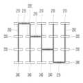
먼저 도 6을 참조하면, 복수 개의 제1 도전판(210) 중 서로 이웃하는 적어도 어느 한 쌍은, 연결라인(215)에 의해 서로 전기적으로 연결될 수 있다. 이렇게 서로 이웃하는 제1 도전판들(210) 사이에 연결라인(215)을 형성하게 되면, 제1 도전판(210) 사이들 사이에 인덕턴스 성분을 추가할 수 있게 되어, 보다 효율적인 노이즈 차폐를 위한 설계 자유도를 향상시킬 수 있는 장점이 있다. 제1 도전판(210) 뿐만 아니라 나머지 도전판들(220, 230, 240) 역시 연결라인(215)에 의해 이웃하는 한 쌍이 서로 연결되어 인덕턴스 성분이 추가될 수 있음은 물론이다.First, referring to FIG. 6, at least one pair of neighboring ones among the plurality of first
도 6 내지 도 8에 도시된 EBG 구조의 경우에는 제2 영역(200)에 마련되는 모든 도전판들이 관통비아(250)와 연결라인(215)에 의해 제2 영역(200) 내에서 전기적으로 연결되는 구조를 갖는다.In the EBG structure shown in FIGS. 6 to 8, all conductive plates provided in the
반면, 도 9에 도시된 EBG 구조의 경우에는, 몇몇 도전판들이 독립된 패스를 형성하고, 이들 각각이 제1 영역(100)의 그라운드층(110)과 적어도 하나이상의 접속라인(260)에 의해 연결된다.On the other hand, in the EBG structure shown in FIG. 9, several conductive plates form independent paths, each of which is connected to the
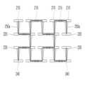
한편, 전술한 실시예들에서는 제2 영역(200)에 마련되는 각각의 도전판들(210, 220, 230, 240)이 제2 영역(200)을 관통하는 관통비아(250)에 의해 전기적으로 연결되는 구조를 제시하였으나, 도 8 및 도 9에 도시된 바와 같이 블라인드 비아(250a)에 의해 개별적으로 연결될 수도 있다.Meanwhile, in the above-described embodiments, each of the
도 10을 참조하면, 제2 영역(200)의 제1 도전판(210)만이 제1 영역(100)의 최상층, 즉 그라운드층(110)과 접속라인(260)에 의해 접속되는 구조가 제시되어 있다. 그러나 본 발명이 이러한 구조에 한정되는 것은 아니며, 도 11에 도시된 바와 같이 제2 영역의 다른 도전판 역시 접속라인에 의해 제1 영역의 다른 층에 연결될 수도 있다. 나아가, 도 12에 도시된 바와 같이, 제1 영역과 제2 영역의 최하층이 접속라인에 의해 서로 직접 연결될 수도 있다.Referring to FIG. 10, a structure in which only the first
도 13 내지 도 15는 도 10 내지 도 12에 각각 대응되는 구조를 나타내는 것으로서, 도 10 내지 도 12의 관통비아(250)가 블라인드 비아(250a)로 대체된 모습을 나타낸다.13 to 15 show a structure corresponding to FIGS. 10 to 12, respectively, in which the through
한편, 도 16에 도시된 바와 같이 제1 영역(100)의 측면이 사각형의 형상을 갖는 경우에는, 제2 영역(200)의 제1 도전판(210) 역시 직사각형의 형상을 가질 것이나, 도 17과 내지 도 19에 도시된 바와 같이 제1 영역(100)이 사각형 이외의 형상을 갖는 경우에는, 제2 영역(200)의 제1 도전판(210) 역시 이에 상응하여 그 외곽이 절곡된 형상을 가질 수 있다. 즉, 도 17에 도시된 바와 같이, 제1 도전판(210)이 절곡된 형상을 갖거나, 도 18에 도시된 바와 같이 곡면을 가질 수도 있 고, 도 19에 도시된 바와 같이 연속적으로 배치되는 삼각형 형상을 가질 수도 있다.Meanwhile, as shown in FIG. 16, when the side surface of the
한편, 내부에 EBG 구조가 삽입되는 제2 영역(200)은 제1 영역(100)의 측면 전체에 걸쳐 배치될 수도 있으나, 특정 부분에만 선택적으로 배치될 수도 있다. 이와 같이 특정 부분에만 제2 영역(200)을 선택적으로 배치함으로써, 사용자가 원하는 부분에 대해서만 선택적으로 노이즈를 차폐할 수 있으며, 비용절감의 효과를 기대할 수 있다.Meanwhile, the
상기에서는 본 발명의 바람직한 실시예를 참조하여 설명하였지만, 해당 기술 분야에서 통상의 지식을 가진 자라면 하기의 특허 청구의 범위에 기재된 본 발명의 사상 및 영역으로부터 벗어나지 않는 범위 내에서 본 발명을 다양하게 수정 및 변경시킬 수 있음을 이해할 수 있을 것이다.It will be apparent to those skilled in the art that various modifications and variations can be made in the present invention without departing from the spirit or scope of the invention as defined in the appended claims. It will be understood that the invention may be varied and varied without departing from the scope of the invention.
전술한 실시예 외의 많은 실시예들이 본 발명의 특허청구범위 내에 존재한다.Many embodiments other than the above-described embodiments are within the scope of the claims of the present invention.
도 1은 전자소자가 실장된 인쇄회로기판에서 노이즈가 방사되는 모습을 나타내는 도면.1 is a diagram illustrating a state in which noise is radiated from a printed circuit board on which an electronic device is mounted.
도 2는 본 발명의 일 실시예에 따른 EMI 노이즈 저감 인쇄회로기판을 나타내는 단면도.Figure 2 is a cross-sectional view showing an EMI noise reduction printed circuit board according to an embodiment of the present invention.
도 3은 본 발명의 일 실시예에 따른 EMI 노이즈 저감 인쇄회로기판을 나타내는 측면도.Figure 3 is a side view showing an EMI noise reduction printed circuit board according to an embodiment of the present invention.
도 4는 본 발명의 일 실시예에 따른 EMI 노이즈 저감 인쇄회로기판을 나타내는 정면도.Figure 4 is a front view showing an EMI noise reduction printed circuit board according to an embodiment of the present invention.
도 5는 본 발명의 일 실시예에 따른 EMI 노이즈 저감 인쇄회로기판을 나타내는 사시도.5 is a perspective view showing an EMI noise reduction printed circuit board according to an embodiment of the present invention.
도 6 내지 도 15는 본 발명의 다양한 실시예에 따른 EMI 노이즈 저감 인쇄회로기판을 나타내는 정면도.6 to 15 are front views illustrating EMI noise reduction printed circuit boards according to various embodiments of the present disclosure.
도 16 내지 도 18은 본 발명의 다양한 실시예에 따른 EMI 노이즈 저감 인쇄회로기판을 나타내는 평면도.16 to 18 are plan views illustrating EMI noise reduction printed circuit boards according to various embodiments of the present disclosure.
<도면의 주요부분에 대한 부호의 설명><Description of the symbols for the main parts of the drawings>
100: 제1 영역200: 제2 영역100: first region 200: second region
210: 제1 도전판215: 연결라인210: first conductive plate 215: connection line
220: 제2 도전판250: 관통비아220: second conductive plate 250: through via
260: 접속라인260: connection line
Claims (7)
Translated fromKoreanPriority Applications (2)
| Application Number | Priority Date | Filing Date | Title |
|---|---|---|---|
| KR1020090089666AKR101021552B1 (en) | 2009-09-22 | 2009-09-22 | EMI noise reduction printed circuit board |
| US12/654,371US20110069470A1 (en) | 2009-09-22 | 2009-12-17 | Electromagnetic interference noise reduction board using electromagnetic bandgap structure |
Applications Claiming Priority (1)
| Application Number | Priority Date | Filing Date | Title |
|---|---|---|---|
| KR1020090089666AKR101021552B1 (en) | 2009-09-22 | 2009-09-22 | EMI noise reduction printed circuit board |
Publications (1)
| Publication Number | Publication Date |
|---|---|
| KR101021552B1true KR101021552B1 (en) | 2011-03-16 |
Family
ID=43756463
Family Applications (1)
| Application Number | Title | Priority Date | Filing Date |
|---|---|---|---|
| KR1020090089666AExpired - Fee RelatedKR101021552B1 (en) | 2009-09-22 | 2009-09-22 | EMI noise reduction printed circuit board |
Country Status (2)
| Country | Link |
|---|---|
| US (1) | US20110069470A1 (en) |
| KR (1) | KR101021552B1 (en) |
Cited By (1)
| Publication number | Priority date | Publication date | Assignee | Title |
|---|---|---|---|---|
| US8952265B2 (en) | 2011-08-22 | 2015-02-10 | Samsung Electro-Mechanics Co., Ltd. | Electromagnetic interference noise reduction package board |
Families Citing this family (3)
| Publication number | Priority date | Publication date | Assignee | Title |
|---|---|---|---|---|
| KR101007288B1 (en)* | 2009-07-29 | 2011-01-13 | 삼성전기주식회사 | Printed Circuit Boards and Electronics |
| US9247647B1 (en)* | 2014-09-11 | 2016-01-26 | Qualcomm Incorporated | High quality factor inductor and high quality factor filter in package substrate or printed circuit board (PCB) |
| CN119521521A (en)* | 2023-08-22 | 2025-02-25 | 宏启胜精密电子(秦皇岛)有限公司 | Circuit board and method for manufacturing the same |
Citations (4)
| Publication number | Priority date | Publication date | Assignee | Title |
|---|---|---|---|---|
| US20050104678A1 (en) | 2003-09-11 | 2005-05-19 | Shahrooz Shahparnia | System and method for noise mitigation in high speed printed circuit boards using electromagnetic bandgap structures |
| KR20080061950A (en)* | 2006-12-28 | 2008-07-03 | 주식회사 하이닉스반도체 | Multilayer PCB with Electromagnetic Bandgap Power Delivery System |
| WO2008127196A1 (en) | 2007-04-12 | 2008-10-23 | Agency For Science, Technology And Research | Composite structure for an electronic circuit |
| KR20090081571A (en)* | 2008-01-24 | 2009-07-29 | 한국과학기술원 | Semiconductor Package Substrate with Double Stacked Electromagnetic Bandgap Structure Around Via Hole |
Family Cites Families (4)
| Publication number | Priority date | Publication date | Assignee | Title |
|---|---|---|---|---|
| US6476771B1 (en)* | 2001-06-14 | 2002-11-05 | E-Tenna Corporation | Electrically thin multi-layer bandpass radome |
| US7626216B2 (en)* | 2005-10-21 | 2009-12-01 | Mckinzie Iii William E | Systems and methods for electromagnetic noise suppression using hybrid electromagnetic bandgap structures |
| US8159413B2 (en)* | 2006-11-01 | 2012-04-17 | Agency For Science, Technology And Research | Double-stacked EBG structure |
| KR100851075B1 (en)* | 2007-04-30 | 2008-08-12 | 삼성전기주식회사 | Electromagnetic Bandgap Structures and Printed Circuit Boards |
- 2009
- 2009-09-22KRKR1020090089666Apatent/KR101021552B1/ennot_activeExpired - Fee Related
- 2009-12-17USUS12/654,371patent/US20110069470A1/ennot_activeAbandoned
Patent Citations (4)
| Publication number | Priority date | Publication date | Assignee | Title |
|---|---|---|---|---|
| US20050104678A1 (en) | 2003-09-11 | 2005-05-19 | Shahrooz Shahparnia | System and method for noise mitigation in high speed printed circuit boards using electromagnetic bandgap structures |
| KR20080061950A (en)* | 2006-12-28 | 2008-07-03 | 주식회사 하이닉스반도체 | Multilayer PCB with Electromagnetic Bandgap Power Delivery System |
| WO2008127196A1 (en) | 2007-04-12 | 2008-10-23 | Agency For Science, Technology And Research | Composite structure for an electronic circuit |
| KR20090081571A (en)* | 2008-01-24 | 2009-07-29 | 한국과학기술원 | Semiconductor Package Substrate with Double Stacked Electromagnetic Bandgap Structure Around Via Hole |
Cited By (1)
| Publication number | Priority date | Publication date | Assignee | Title |
|---|---|---|---|---|
| US8952265B2 (en) | 2011-08-22 | 2015-02-10 | Samsung Electro-Mechanics Co., Ltd. | Electromagnetic interference noise reduction package board |
Also Published As
| Publication number | Publication date |
|---|---|
| US20110069470A1 (en) | 2011-03-24 |
Similar Documents
| Publication | Publication Date | Title |
|---|---|---|
| KR101072591B1 (en) | Electromagnetic interference noise reduction board using electromagnetic bandgap structure | |
| KR101023541B1 (en) | EMI noise reduction printed circuit board | |
| US8952265B2 (en) | Electromagnetic interference noise reduction package board | |
| KR101007288B1 (en) | Printed Circuit Boards and Electronics | |
| EP1895826B1 (en) | Electronic Appliance with a metallic heat dissipating member | |
| US8699234B2 (en) | EMI noise shield board including electromagnetic bandgap structure | |
| KR101021548B1 (en) | Printed Circuit Board with Electromagnetic Bandgap Structure | |
| US20050104678A1 (en) | System and method for noise mitigation in high speed printed circuit boards using electromagnetic bandgap structures | |
| KR101038236B1 (en) | printed circuit board having electromagnetic bandgap structure | |
| JP4736988B2 (en) | Multilayer printed circuit board | |
| US20130176683A1 (en) | Electronic assembly | |
| US8232478B2 (en) | Electromagnetic interference noise reduction board using electromagnetic bandgap structure | |
| KR101021552B1 (en) | EMI noise reduction printed circuit board | |
| KR101046716B1 (en) | Electromagnetic bandgap structures and circuit boards | |
| KR101092590B1 (en) | Printed Circuit Board with Electromagnetic Bandgap Structure | |
| KR101021551B1 (en) | Printed Circuit Board with Electromagnetic Bandgap Structure | |
| KR101422931B1 (en) | Muti-layer Printed Circuit Board | |
| JP4816274B2 (en) | LSI shielding device, LSI shielding method, LSI package | |
| KR20080064620A (en) | Printed circuit board | |
| JP2015005716A (en) | Multilayer printed circuit board |
Legal Events
| Date | Code | Title | Description |
|---|---|---|---|
| A201 | Request for examination | ||
| PA0109 | Patent application | St.27 status event code:A-0-1-A10-A12-nap-PA0109 | |
| PA0201 | Request for examination | St.27 status event code:A-1-2-D10-D11-exm-PA0201 | |
| E701 | Decision to grant or registration of patent right | ||
| GRNT | Written decision to grant | ||
| PE0701 | Decision of registration | St.27 status event code:A-1-2-D10-D22-exm-PE0701 | |
| PR0701 | Registration of establishment | St.27 status event code:A-2-4-F10-F11-exm-PR0701 | |
| PR1002 | Payment of registration fee | St.27 status event code:A-2-2-U10-U11-oth-PR1002 Fee payment year number:1 | |
| PG1601 | Publication of registration | St.27 status event code:A-4-4-Q10-Q13-nap-PG1601 | |
| FPAY | Annual fee payment | Payment date:20131224 Year of fee payment:4 | |
| PR1001 | Payment of annual fee | St.27 status event code:A-4-4-U10-U11-oth-PR1001 Fee payment year number:4 | |
| R18-X000 | Changes to party contact information recorded | St.27 status event code:A-5-5-R10-R18-oth-X000 | |
| FPAY | Annual fee payment | Payment date:20150202 Year of fee payment:5 | |
| PR1001 | Payment of annual fee | St.27 status event code:A-4-4-U10-U11-oth-PR1001 Fee payment year number:5 | |
| LAPS | Lapse due to unpaid annual fee | ||
| PC1903 | Unpaid annual fee | St.27 status event code:A-4-4-U10-U13-oth-PC1903 Not in force date:20160305 Payment event data comment text:Termination Category : DEFAULT_OF_REGISTRATION_FEE | |
| PC1903 | Unpaid annual fee | St.27 status event code:N-4-6-H10-H13-oth-PC1903 Ip right cessation event data comment text:Termination Category : DEFAULT_OF_REGISTRATION_FEE Not in force date:20160305 | |
| R18-X000 | Changes to party contact information recorded | St.27 status event code:A-5-5-R10-R18-oth-X000 |