KR101018850B1 - Susceptor Plates for High Temperature Heat Treatment - Google Patents
Susceptor Plates for High Temperature Heat TreatmentDownload PDFInfo
- Publication number
- KR101018850B1 KR101018850B1KR1020030060106AKR20030060106AKR101018850B1KR 101018850 B1KR101018850 B1KR 101018850B1KR 1020030060106 AKR1020030060106 AKR 1020030060106AKR 20030060106 AKR20030060106 AKR 20030060106AKR 101018850 B1KR101018850 B1KR 101018850B1
- Authority
- KR
- South Korea
- Prior art keywords
- wafer
- susceptor plate
- susceptor
- support surface
- wafers
- Prior art date
- Legal status (The legal status is an assumption and is not a legal conclusion. Google has not performed a legal analysis and makes no representation as to the accuracy of the status listed.)
- Expired - Lifetime
Links
- 238000010438heat treatmentMethods0.000titleclaimsdescription5
- 238000000034methodMethods0.000claimsabstractdescription34
- 238000012545processingMethods0.000claimsabstractdescription27
- XUIMIQQOPSSXEZ-UHFFFAOYSA-NSiliconChemical compound[Si]XUIMIQQOPSSXEZ-UHFFFAOYSA-N0.000claimsabstractdescription12
- 229910052710siliconInorganic materials0.000claimsabstractdescription12
- 239000010703siliconSubstances0.000claimsabstractdescription12
- 235000012431wafersNutrition0.000claimsdescription120
- 239000000463materialSubstances0.000claimsdescription14
- 238000011282treatmentMethods0.000claimsdescription10
- 239000004065semiconductorSubstances0.000claimsdescription5
- 238000001816coolingMethods0.000claimsdescription4
- 238000011068loading methodMethods0.000claimsdescription4
- 238000000227grindingMethods0.000claimsdescription3
- 238000005498polishingMethods0.000claimsdescription3
- 238000007665saggingMethods0.000abstractdescription12
- 238000010923batch productionMethods0.000abstract2
- 230000035882stressEffects0.000description18
- 238000005229chemical vapour depositionMethods0.000description11
- 238000005452bendingMethods0.000description5
- 230000000694effectsEffects0.000description4
- NJPPVKZQTLUDBO-UHFFFAOYSA-NnovaluronChemical compoundC1=C(Cl)C(OC(F)(F)C(OC(F)(F)F)F)=CC=C1NC(=O)NC(=O)C1=C(F)C=CC=C1FNJPPVKZQTLUDBO-UHFFFAOYSA-N0.000description4
- 230000007423decreaseEffects0.000description3
- 238000003754machiningMethods0.000description3
- 239000011248coating agentSubstances0.000description2
- 238000000576coating methodMethods0.000description2
- 238000000151depositionMethods0.000description2
- 230000008021depositionEffects0.000description2
- 239000012636effectorSubstances0.000description2
- OKTJSMMVPCPJKN-UHFFFAOYSA-NCarbonChemical compound[C]OKTJSMMVPCPJKN-UHFFFAOYSA-N0.000description1
- 238000007792additionMethods0.000description1
- 230000008602contractionEffects0.000description1
- 230000001419dependent effectEffects0.000description1
- 238000013461designMethods0.000description1
- 238000003795desorptionMethods0.000description1
- 230000005489elastic deformationEffects0.000description1
- 229910002804graphiteInorganic materials0.000description1
- 239000010439graphiteSubstances0.000description1
- 230000005484gravityEffects0.000description1
- 239000002184metalSubstances0.000description1
- 238000012986modificationMethods0.000description1
- 230000004048modificationEffects0.000description1
- 229910021421monocrystalline siliconInorganic materials0.000description1
- 230000001151other effectEffects0.000description1
- 238000013021overheatingMethods0.000description1
- 230000005855radiationEffects0.000description1
- 239000000758substrateSubstances0.000description1
- 230000008646thermal stressEffects0.000description1
Images


Classifications
- H—ELECTRICITY
- H01—ELECTRIC ELEMENTS
- H01L—SEMICONDUCTOR DEVICES NOT COVERED BY CLASS H10
- H01L21/00—Processes or apparatus adapted for the manufacture or treatment of semiconductor or solid state devices or of parts thereof
- H01L21/02—Manufacture or treatment of semiconductor devices or of parts thereof
- H01L21/04—Manufacture or treatment of semiconductor devices or of parts thereof the devices having potential barriers, e.g. a PN junction, depletion layer or carrier concentration layer
- H01L21/18—Manufacture or treatment of semiconductor devices or of parts thereof the devices having potential barriers, e.g. a PN junction, depletion layer or carrier concentration layer the devices having semiconductor bodies comprising elements of Group IV of the Periodic Table or AIIIBV compounds with or without impurities, e.g. doping materials
- H01L21/30—Treatment of semiconductor bodies using processes or apparatus not provided for in groups H01L21/20 - H01L21/26
- H01L21/324—Thermal treatment for modifying the properties of semiconductor bodies, e.g. annealing, sintering
- H—ELECTRICITY
- H01—ELECTRIC ELEMENTS
- H01L—SEMICONDUCTOR DEVICES NOT COVERED BY CLASS H10
- H01L21/00—Processes or apparatus adapted for the manufacture or treatment of semiconductor or solid state devices or of parts thereof
- H01L21/67—Apparatus specially adapted for handling semiconductor or electric solid state devices during manufacture or treatment thereof; Apparatus specially adapted for handling wafers during manufacture or treatment of semiconductor or electric solid state devices or components ; Apparatus not specifically provided for elsewhere
- H01L21/673—Apparatus specially adapted for handling semiconductor or electric solid state devices during manufacture or treatment thereof; Apparatus specially adapted for handling wafers during manufacture or treatment of semiconductor or electric solid state devices or components ; Apparatus not specifically provided for elsewhere using specially adapted carriers or holders; Fixing the workpieces on such carriers or holders
- H01L21/67303—Vertical boat type carrier whereby the substrates are horizontally supported, e.g. comprising rod-shaped elements
- H01L21/67309—Vertical boat type carrier whereby the substrates are horizontally supported, e.g. comprising rod-shaped elements characterized by the substrate support
- H—ELECTRICITY
- H01—ELECTRIC ELEMENTS
- H01L—SEMICONDUCTOR DEVICES NOT COVERED BY CLASS H10
- H01L21/00—Processes or apparatus adapted for the manufacture or treatment of semiconductor or solid state devices or of parts thereof
- H01L21/67—Apparatus specially adapted for handling semiconductor or electric solid state devices during manufacture or treatment thereof; Apparatus specially adapted for handling wafers during manufacture or treatment of semiconductor or electric solid state devices or components ; Apparatus not specifically provided for elsewhere
- H01L21/683—Apparatus specially adapted for handling semiconductor or electric solid state devices during manufacture or treatment thereof; Apparatus specially adapted for handling wafers during manufacture or treatment of semiconductor or electric solid state devices or components ; Apparatus not specifically provided for elsewhere for supporting or gripping
- H01L21/687—Apparatus specially adapted for handling semiconductor or electric solid state devices during manufacture or treatment thereof; Apparatus specially adapted for handling wafers during manufacture or treatment of semiconductor or electric solid state devices or components ; Apparatus not specifically provided for elsewhere for supporting or gripping using mechanical means, e.g. chucks, clamps or pinches
- H01L21/68714—Apparatus specially adapted for handling semiconductor or electric solid state devices during manufacture or treatment thereof; Apparatus specially adapted for handling wafers during manufacture or treatment of semiconductor or electric solid state devices or components ; Apparatus not specifically provided for elsewhere for supporting or gripping using mechanical means, e.g. chucks, clamps or pinches the wafers being placed on a susceptor, stage or support
- H01L21/68735—Apparatus specially adapted for handling semiconductor or electric solid state devices during manufacture or treatment thereof; Apparatus specially adapted for handling wafers during manufacture or treatment of semiconductor or electric solid state devices or components ; Apparatus not specifically provided for elsewhere for supporting or gripping using mechanical means, e.g. chucks, clamps or pinches the wafers being placed on a susceptor, stage or support characterised by edge profile or support profile
- H—ELECTRICITY
- H01—ELECTRIC ELEMENTS
- H01L—SEMICONDUCTOR DEVICES NOT COVERED BY CLASS H10
- H01L21/00—Processes or apparatus adapted for the manufacture or treatment of semiconductor or solid state devices or of parts thereof
- H01L21/67—Apparatus specially adapted for handling semiconductor or electric solid state devices during manufacture or treatment thereof; Apparatus specially adapted for handling wafers during manufacture or treatment of semiconductor or electric solid state devices or components ; Apparatus not specifically provided for elsewhere
- H01L21/683—Apparatus specially adapted for handling semiconductor or electric solid state devices during manufacture or treatment thereof; Apparatus specially adapted for handling wafers during manufacture or treatment of semiconductor or electric solid state devices or components ; Apparatus not specifically provided for elsewhere for supporting or gripping
- H01L21/687—Apparatus specially adapted for handling semiconductor or electric solid state devices during manufacture or treatment thereof; Apparatus specially adapted for handling wafers during manufacture or treatment of semiconductor or electric solid state devices or components ; Apparatus not specifically provided for elsewhere for supporting or gripping using mechanical means, e.g. chucks, clamps or pinches
- H01L21/68714—Apparatus specially adapted for handling semiconductor or electric solid state devices during manufacture or treatment thereof; Apparatus specially adapted for handling wafers during manufacture or treatment of semiconductor or electric solid state devices or components ; Apparatus not specifically provided for elsewhere for supporting or gripping using mechanical means, e.g. chucks, clamps or pinches the wafers being placed on a susceptor, stage or support
- H01L21/6875—Apparatus specially adapted for handling semiconductor or electric solid state devices during manufacture or treatment thereof; Apparatus specially adapted for handling wafers during manufacture or treatment of semiconductor or electric solid state devices or components ; Apparatus not specifically provided for elsewhere for supporting or gripping using mechanical means, e.g. chucks, clamps or pinches the wafers being placed on a susceptor, stage or support characterised by a plurality of individual support members, e.g. support posts or protrusions
Landscapes
- Engineering & Computer Science (AREA)
- Physics & Mathematics (AREA)
- Condensed Matter Physics & Semiconductors (AREA)
- General Physics & Mathematics (AREA)
- Manufacturing & Machinery (AREA)
- Computer Hardware Design (AREA)
- Microelectronics & Electronic Packaging (AREA)
- Power Engineering (AREA)
- Container, Conveyance, Adherence, Positioning, Of Wafer (AREA)
Abstract
Translated fromKorean
Description
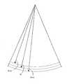
Translated fromKorean도 1은 반도체 웨이퍼의 측면과 같이 만곡의 반경을 따라 굽혀지거나 휜 물체를 나타내며, 1 illustrates an object that is bent or curved along a radius of curvature, such as the side of a semiconductor wafer,
도 2는 굽혀진 물체의 휘어짐(deflection)을 나타내며, 2 shows the deflection of the curved object,
도 3은 평탄 표면위의 돌출부와 돌출부에 지지된 물체에 대한 영향을 나타내며, 3 shows the protrusion on the flat surface and the effect on the object supported on the protrusion,
도 4는 서셉터 플레이트 홀더내의 서셉터 플레이트의 3개 부분의 지지를 나타내며, 4 shows the support of three parts of the susceptor plate in the susceptor plate holder,
도 5A는 장착되지 않은 미리-굽혀진 서셉터 플레이트를 나타내는 도 4의 A-A선을 따른 개략적인 측면도를 나타내며, 5A shows a schematic side view along line A-A of FIG. 4 showing an unmounted pre-bend susceptor plate, FIG.
도 5B는 도 4의 서셉터 플레이트 홀더내에 장착되었을 때, 자체 무게의 새깅에 의해 굽혀진 정도가 감소한 미리-굽혀진 서셉터 플레이트을 나타내는 도 4의 A-A선을 따른 개략적인 측면도를 나타내며, FIG. 5B shows a schematic side view along line A-A of FIG. 4 showing a pre-bend susceptor plate having a reduced degree of bending by sagging of its own weight when mounted in the susceptor plate holder of FIG. 4, FIG.
도 6A는 장착되지 않은 미리-굽혀진 서셉터 플레이트를 나타내는, 도 4의 B-B선을 따른 개략적인 측면도를 나타내며,FIG. 6A shows a schematic side view along line B-B of FIG. 4, showing a pre-bent susceptor plate not mounted; FIG.
도 6B는 도 7의 서셉터 플레이트 홀더내에 장착되었을 때, 자체의 무게의 새깅에 의해 굽혀진 정도가 감소한 미리-굽혀진 서셉터 플레이트를 나타내는 도 4의 B-B선을 따른 굽힘을 나타내며,FIG. 6B shows the bending along line B-B of FIG. 4 showing the pre-bend susceptor plate having a reduced degree of bending by sagging of its weight when mounted in the susceptor plate holder of FIG. 7, FIG.
도 7은 본 발명의 제 1실시예에 따라 만들어진 서셉터 플레이트를 나타내는 평면도와 여러 국부적인 단면을 나타내는 측면도이고,7 is a plan view showing a susceptor plate made according to a first embodiment of the present invention and a side view showing several local cross sections,
도 8은 도 7의 서셉터 플레이트의 개략적인 단면도(스케일은 맞지 않음)이고,FIG. 8 is a schematic cross-sectional view (not scaled) of the susceptor plate of FIG. 7,
도 9는 본 발명의 제 2실시예에 따라 만들어진 서셉터 플레이트를 나타내는 평면도와 여러 국부적인 단면을 나타내는 측면도이고,9 is a plan view showing a susceptor plate made according to a second embodiment of the present invention and a side view showing several local cross sections,
도 10은 본 발명의 제 3실시예에 따라 만들어진 서셉터 플레이트를 나타내는 평면도와 여러 국부적인 단면을 나타내는 측면도이다.10 is a plan view showing a susceptor plate made in accordance with a third embodiment of the present invention and a side view showing several local cross sections.
본 발명은, 퍼니스 내에서 고온에서 반도체 웨이퍼를 배치 처리(batch treatment)하는 분야에 관한 것이다. 수직형 퍼니스 내에서 반도체 웨이퍼를 처리하는 동안에, 비교적 많은 수의 웨이퍼가 수직방향으로 이격된 관계를 가지면서, 수평으로 배향된 웨이퍼 보트 내에 수용된다. 표준 웨이퍼 보트 내에서, 웨이퍼는 3 개 이상의 주변부(웨이퍼의 가장자리)에서 지지된다. 그러나, 고온(예를 들면, > 1000℃)에서는 웨이퍼의 항복응력(yied stress)이 감소하고, 자체의 무게로 인해 처지거나, 열적으로 유도된 응력의 결과로 변형되거나, 두 가지 모두의 영향으로 인하여 변형될 수도 있다. 웨이퍼의 두께가 그 지름에 비례하여 증가하는 것이 아니기 때문에, 직경이 큰 웨이퍼는 직경이 작은 웨이퍼에 비하여 이러한 영향에 더 취약하다. The present invention relates to the field of batch treatment of semiconductor wafers at high temperatures in a furnace. During processing of semiconductor wafers in a vertical furnace, a relatively large number of wafers are accommodated in a horizontally oriented wafer boat, with a vertically spaced relationship. In a standard wafer boat, wafers are supported at three or more perimeters (edges of wafers). However, at high temperatures (eg> 1000 ° C.), the yield stress of the wafer decreases, sags due to its own weight, deforms as a result of thermally induced stress, or under both influences. May be deformed. Since the thickness of the wafer does not increase in proportion to its diameter, a larger diameter wafer is more vulnerable to this effect than a smaller diameter wafer.
미국특허 제 5,219,079호에서는, 웨이퍼의 휘어짐(warp)을 방지하는 서셉터 플레이트를 포함하는 웨이퍼 보트가 개시되어 있다. 상기 플레이트는 로보트 엔드 이펙터(end effector)로 웨이퍼의 아래 표면과 접촉하여 상기 웨이퍼를 플레이트 상으로 로딩시킬 수 있는 큰 오목부(recess)를 가진다. 그러나, 상대적으로 큰 오목부로 인하여 상기 웨이퍼의 국부적인 변형이 초래됨이 발견되었다. 환형 지지보트와 같이 연장된 웨이퍼 지지 영역을 가진 다른 보트들이 제안되어 있다. 그러나, 300mm 웨이퍼를 고온에서 처리하는데는 위 제안된 지지체가 적당하지 아니하며 여전히 웨이퍼들의 소성변형을 야기한다.In US Pat. No. 5,219,079, a wafer boat is disclosed that includes a susceptor plate that prevents warp of the wafer. The plate has a large recess that can contact the bottom surface of the wafer with a robot end effector to load the wafer onto the plate. However, it has been found that the relatively large recesses result in local deformation of the wafer. Other boats with extended wafer support areas, such as annular support boats, have been proposed. However, the above proposed support is not suitable for processing 300mm wafers at high temperature and still cause plastic deformation of the wafers.
다른 노력으로 일본특허 제 63102225호에서는 웨이퍼의 아래 전체 표면을 지지하는 서셉터 플레이트를 포함하는 웨이퍼보트가 개시되어 있다. 이 보트는 반응성 가스 난류를 웨이퍼로부터 멀리하게 하고 이로써 웨이퍼 위에 화학기상증착 (CVD)으로 증착된 막의 균일성을 개선한다. 웨이퍼는 수동으로 서셉터 플레이트에 장착될 필요가 있다. 이것은 오늘날의 공정에서는 허용될 수 없으며, 이 경우, 300mm 웨이퍼를 수동으로 취급하는 것은 작업이 용이한 선택이 아니다.In another effort, Japanese Patent No. 63102225 discloses a wafer boat including a susceptor plate that supports the entire lower surface of the wafer. This boat keeps reactive gas turbulence away from the wafer, thereby improving the uniformity of the film deposited by chemical vapor deposition (CVD) on the wafer. The wafer needs to be mounted to the susceptor plate manually. This is unacceptable in today's process, in which case handling 300 mm wafers manually is not an easy choice.
따라서, 본 발명의 목적은 300mm 웨이퍼를 1000℃이상의 온도에서, 웨이퍼가 자동으로 다루어지고 웨이퍼의 소성변형이 최소화되거나 제거되는 방법과 장치를 제공하는 것이다.Accordingly, it is an object of the present invention to provide a method and apparatus in which a wafer is automatically handled and the plastic deformation of the wafer is minimized or eliminated at a temperature of 300 mm wafers above 1000 ° C.
본 발명에 따르면, 공정 동안에 웨이퍼 보트내에서 웨이퍼는 수직방향으로 떨어져서 수용되며, 웨이퍼는 서셉터 플레이트에 의해 충분히 전체 아래 표면이 지지된다. 서셉터 플레이트가 웨이퍼 보트에 수용되고 300mm 웨이퍼를 장착하면, 서셉터 플레이트는 공정동안 웨이퍼의 슬립(slip)을 최소화하는 한계내의 전체 평탄도(overall flatness)를 가진다.According to the present invention, during the process, the wafers are received away vertically in the wafer boat, and the wafer is fully supported by the susceptor plate to fully support the bottom surface. Once the susceptor plate is housed in a wafer boat and loaded with a 300 mm wafer, the susceptor plate has an overall flatness within limits that minimizes the slip of the wafer during processing.
설명되는 실시예에서, 서셉터 플레이트위로 웨이퍼의 자동장착을 쉽게 하기 위하여, 플레이트는 20mm를 넘지 않는 직경의 3개 또는 그 이상의 홀을 갖는 것이 바람직하다. 서셉터 플레이트의 지지표면의 돌출부는 국부적인 슬립의 발생을 방지하기 위해 0.7㎛보다 작은 높이를 갖는 것이 바람직하다.In the described embodiment, in order to facilitate the automatic loading of the wafer onto the susceptor plate, the plate preferably has three or more holes of diameter not exceeding 20 mm. The protrusion of the support surface of the susceptor plate preferably has a height of less than 0.7 mu m to prevent the occurrence of local slip.
관계되는 미국출원 제 60/365,122호에 본 발명의 서셉터 플레이트위에 웨이퍼를 자동적으로 장착하는 방법과 장치가 개시되어 있다.Related US application 60 / 365,122 discloses a method and apparatus for automatically mounting a wafer on a susceptor plate of the present invention.
수직 퍼니스내에서 실리콘 웨이퍼의 고온 공정중에 결정학적 슬립(crystallographic slip)을 방지하기 위해서는, 웨이퍼의 전체면적이 충분히 지지되어야 하는 것이 발견되었다. 이 지지는 서셉터 플레이트 홀더에 분리가능하게 수용되는 서셉터 플레이트에 의해 제공된다. 서셉터 플레이트 홀더는 표준 개방 웨이퍼 보트와 유사하게 설계되며 최소한 3개의 수직 칼럼을 포함하는데, 칼럼의 위쪽 끝은 위쪽 플레이트에 부착되고 칼럼의 아래쪽 끝은 아래쪽 플레이트에 부착되는데, 각 칼럼은 서셉터 플레이트가 수직방향으로 이격되어 있고 홀더내에서 거 의 수평으로 위치할수 있게 하기 위하여 서셉터 플레이트의 모서리를 수용하기 위한 상호 이격된 오목부를 가진다. 여기서 서셉터라는 용어의 사용은 플레이트가 방사열 또는 유도열을 흡수하도록 만들어져야 하는 것을 의미하는 것은 아니다. 당업자는 이해하겠지만, 여기서 설명된 서셉터 플레이트가 지지된 기판에 열적 영향을 주지 않는다 하더라도, 여기서 설명된 바와 같이 형성될 수 있으며 여기서 설명된 이점을 얻을 수 있다.In order to prevent crystallographic slip during high temperature processing of silicon wafers in a vertical furnace, it has been found that the entire area of the wafer must be sufficiently supported. This support is provided by a susceptor plate detachably received in the susceptor plate holder. The susceptor plate holder is designed similar to a standard open wafer boat and includes at least three vertical columns, with the top end of the column attached to the top plate and the bottom end of the column attached to the bottom plate, with each column attached to the susceptor plate. Have spaced apart recesses for receiving the edges of the susceptor plate so that they can be spaced vertically and positioned almost horizontally in the holder. The use of the term susceptor herein does not mean that the plate must be made to absorb radiant or induced heat. As will be appreciated by those skilled in the art, although the susceptor plate described herein does not have a thermal effect on the supported substrate, it can be formed as described herein and the advantages described herein can be obtained.
서셉터 플레이트위로의 웨이퍼 장착과 서셉터 플레이트로부터의 웨이퍼 탈착을 용이하게 하기 위하여, 각 서셉터 플레이트는 리프팅 핀(lifting pin)이 서셉터 플레이트의 아래쪽 면으로부터 통과하도록 복수의 관통공을 가지는 것이 바람직하다. 관통공은 서로 이격되며 관통공을 향하는(pointing through) 3개의 리프팅 핀으로 지지되는 웨이퍼가 안정되게 지지되도록 위치하는 것이 바람직하다. 각 관통공의 직경은 슬립의 발생을 방지하기 위하여 20mm이하인 것이 바람직하며, 관통공의 직경은 10mm이하인 것이 더욱 바람직하다.In order to facilitate wafer mounting onto the susceptor plate and removal of the wafer from the susceptor plate, each susceptor plate preferably has a plurality of through holes so that the lifting pins pass from the bottom surface of the susceptor plate. Do. The through holes are preferably positioned so that the wafers supported by three lifting pins spaced apart from each other and pointing through the holes are stably supported. The diameter of each through hole is preferably 20 mm or less in order to prevent the occurrence of slip, and more preferably, the diameter of the through hole is 10 mm or less.
중력응력 또는 열적응력은 웨이퍼의 변형을 가져온다. 변형이 작으면 그 변형은 탄성적이다. 이것은 응력이 제거되면, 웨이퍼는 본래의 평탄한 형상을 되찾는 것을 의미한다. 그러나, 웨이퍼내의 응력이 항복응력을 초과하면, 웨이퍼는 소성적으로 변형한다. 이것은 변형의 일부분이 영구적이라는 것을 의미한다. 미세한 스케일에서는 결정학적 슬립이 발생한다. 웨이퍼의 항복응력은 온도에 의존하며 온도의 증가에 따라 감소한다. 이 이유 때문에 고온 처리는 매우 민감하다. 처리 온도가 높아질수록, 웨이퍼가 견딜수 있는 변형은 작아진다. 아래에 허용되는 변형이 나와 있다.Gravity or thermal stresses result in deformation of the wafer. If the deformation is small, the deformation is elastic. This means that once the stress is removed, the wafer regains its original flat shape. However, if the stress in the wafer exceeds the yield stress, the wafer deforms plastically. This means that part of the deformation is permanent. At fine scale, crystallographic slip occurs. The yield stress of the wafer is temperature dependent and decreases with increasing temperature. For this reason, high temperature treatment is very sensitive. The higher the processing temperature, the smaller the deformation that the wafer can withstand. Allowed variants are shown below.
평탄한 플레이트가 원통형 형상을(도 1에 플레이트의 측면이 나와 있다) 가지도록 약간 변형되었다고 생각하자. 플레이트의 중앙 면(반경=R)은 도 1과 같이 플레이트가 휘어졌을 때 늘어나거나 줄어들지 않지만, 위쪽 표면(반경=R-d)은 다소 늘어났으며 아래쪽 표면(반경=R+d)은 다소 줄었다. 변형 εs는 다음으로 주어진다.Assume that the flat plate is slightly deformed to have a cylindrical shape (the side of the plate is shown in FIG. 1). The central face (radius = R) of the plate does not stretch or shrink when the plate is bent as shown in FIG. 1, but the upper surface (radius = Rd) is somewhat increased and the lower surface (radius = R + d) is somewhat reduced. The strain εs is given by
εs=σs×(1-ν)/E (1)εs = σs × (1-ν) / E (1)
여기서,here,
σs는 재료의 항복 응력;σs is the yield stress of the material;
E는 영의 모듈러스, 탄성변형의 경우에 응력과 변형의 관계를 정의한다;E defines the relationship between stress and strain in the case of Young's modulus, elastic deformation;
ν는 푸와송의 비.ν is the ratio of Poisson.
1300℃에서 1-0-0 또는 <100> 단일-결정 실리콘은, 다음 값이 적용될 수 있다.For 1-0-0 or <100> single-crystal silicon at 1300 ° C., the following values may be applied.
σs= 0.45 MPaσs = 0.45 MPa
E = 130 GPaE = 130 GPa
ν = 0.28ν = 0.28
식 (1)에 이들 값을 대입하면:Substituting these values into equation (1):
εs= 0.45×106×(1-0.28)/(130×109) = 2.5×10⁻⁶ (2)εs = 0.45 × 106 × (1-0.28) / (130 × 109 ) = 2.5 × 10⁻⁶ (2)
이 스트레인을 만곡(curvature)의 반경에 연관시키겠다. 아래쪽 표면의 수축 은 중앙 평면에서 아래쪽 평면으로 갈 때 반경의 감소에 비례한다. 비슷하게, 위쪽 평면의 신장은 중앙 평면에서 위쪽 평면으로 갈 때 반경의 증가에 비례한다. 플레이트의 두께를 2d라고 하자. 위쪽 표면과 아래쪽 표면에의 응력은 항복응력보다 작아야 한다. 응력을 항복응력과 같다고 하면 다음의 식이 나온다.
We will associate this strain with the radius of the curvature. The contraction of the bottom surface is proportional to the decrease in radius from the center plane to the bottom plane. Similarly, the elongation of the upper plane is proportional to the increase in radius as it goes from the central plane to the upper plane. Let the thickness of the plate be 2d. The stresses on the upper and lower surfaces shall be less than the yield stress. If the stress is equal to the yield stress, the following equation is obtained.
(R-d) =R =(R+d) (3)(Rd) =R =(R + d) (3)
(1-εs) 1 (1+εs)(1-εs ) 1 (1 + εs )
(3)식의 결과로:As a result of (3):
R = d/εs (4)R = d / εs (4)
표준 실리콘 웨이퍼 두께의 절반을 나타내는 d = 380×10-6m를 대입하면, 결과는:Substituting d = 380 x 10-6 m representing half the standard silicon wafer thickness, the result is:
R = 152mR = 152 m
이것은 1300℃의 처리온도에서 소성변형이 발생하기 시작하는 만곡의 반경이다. 만곡의 반경을 웨이퍼의 휘어짐(deflection)과 관련시킬 수 있다(도 2 참조). 휘어짐 b는 만곡의 반경 R과 웨이퍼 직경 D에 다음과 같이 연관된다:This is the radius of curvature at which plastic deformation begins to occur at a processing temperature of 1300 ° C. The radius of curvature can be related to the deflection of the wafer (see FIG. 2). Curvature b is related to the radius of curvature R and the wafer diameter D as follows:
b = R-a = R-[R2-(0.5D)2]0.5 (5)b = Ra = R- [R2- (0.5D)2 ]0.5 (5)
b = 152-[1522-(150×10-3)2]0.5 = 74×10-6 m (6)b = 152- [1522- (150 × 10-3 )2 ]0.5 = 74 × 10-6 m (6)
같은 방법으로 다른 처리온도에 대한 웨이퍼의 만곡의 허용반경이 계산될 수 있으며 아래의 표 1에 나타나 있다.In the same way the allowable radius of curvature of the wafer for different processing temperatures can be calculated and is shown in Table 1 below.
<표 1>TABLE 1
표 1은 다른 온도에서 실리콘의 응력과 300mm 실리콘 웨이퍼의 소성변형이 시작되는 만곡의 반경 또는 휘어짐을 제공한다. 표 1에서 분명히 나타나듯이, 새깅때문에 받아들여질 수 있는 허용되는 웨이퍼 휘어짐은(서셉터 플레이트 휘어짐의 설계에 의하여 조정된다) 처리온도에 의존한다. 온도가 약 1000℃와 같거나 낮으면 허용되는 휘어짐은 328㎛보다 작은 것이 바람직하다; 온도가 약 1100℃와 같거나 낮으면 허용되는 휘어짐은 200㎛보다 작은 것이 바람직하다; 온도가 약 1200℃와 같거나 낮으면 허용되는 휘어짐은 125㎛보다 작은 것이 바람직하다; 온도가 약 1300℃와 같거나 낮으면 허용되는 휘어짐은 75㎛보다 작은 것이 바람직하다;Table 1 provides the radius of curvature or warpage at which the stress of silicon at different temperatures and the plastic deformation of a 300 mm silicon wafer begins. As is apparent from Table 1, the acceptable wafer deflection (adjusted by the design of susceptor plate deflection) that is acceptable due to sagging depends on the processing temperature. If the temperature is less than or equal to about 1000 ° C., the allowable warpage is preferably less than 328 μm; If the temperature is less than or equal to about 1100 ° C., the allowable warpage is preferably less than 200 μm; If the temperature is less than or equal to about 1200 ° C., the allowable warpage is preferably less than 125 μm; If the temperature is less than or equal to about 1300 ° C., the allowable warpage is preferably less than 75 μm;
처리온도에서 웨이퍼의 처리 도중에, 서셉터 플레이트 홀더내에 있는 서셉터 플레이트위에 지지되어 있는 웨이퍼의 휘어짐이 표 1에 정의된 값보다 작거나 또는 만곡의 반경이 표 1에 정의된 값보다 크면 어떠한 소성변형도 발생하지 않는다. 처리온도의 중간 값, 휘어짐의 중간 값, 그리고 만곡의 반경의 중간 값이 적용가능한 것은 분명하다. 첫번째 근사값으로, 당업자는 주어진 값들 사이의 선형 내삽법을 적용할 수 있다.During the processing of the wafer at the processing temperature, any plastic deformation if the warpage of the wafer supported on the susceptor plate in the susceptor plate holder is less than the value defined in Table 1 or the radius of curvature is greater than the value defined in Table 1 Also does not occur. It is clear that the median of the treatment temperature, the median of the warp, and the median of the radius of curvature are applicable. As a first approximation, one skilled in the art can apply linear interpolation between given values.
굽힘에 의한 웨이퍼내의 기계적 응력에 더하여, 웨이퍼의 온도 기울기에 의한 열적으로 유도된 응력도 발생할 수 있다. 표 1에 주어진 허용되는 휘어짐의 한계는 열적으로 유도된 응력을 0으로 가정하였는데, 실제로는 그렇지 않다. 따라서, 공정중에 서셉터 플레이트위에 지지된 웨이퍼가 표 1에 명시된 평탄도보다 좋은(즉, 낮은 만곡의 반경) 평탄도를 가지는 것이 유리한다. 웨이퍼의 평탄도가 좋을수록 슬립을 유도하지 않는 허용가능한 램프-업 또는 램프-다운 속도가 커진다. 예를 들어, 휘어짐이 25㎛보다 작은 서셉터 플레이트와 함께 사용된 램프속도에 대한 값이 표 2에 나와있는데 함께 사용한 결과 웨이퍼에 슬립이 없어졌다. 최대치를 나타내지 않고 예시적인 값만이 있지만, 본 발명의 개시로부터 주어진 온도범위에서 슬립없이 표 2내의 예시적인 속도보다 낮은 램프속도가 사용될 수 있다는 것이 이해될 것이다.In addition to mechanical stress in the wafer due to bending, thermally induced stress due to the temperature gradient of the wafer may also occur. The allowable deflection limits given in Table 1 assume that the thermally induced stress is zero, which in practice is not. Thus, it is advantageous for the wafer supported on the susceptor plate during the process to have a flatness that is better than the flatness specified in Table 1 (ie, low curvature radius). The better the flatness of the wafer, the higher the acceptable ramp-up or ramp-down speed that does not induce slip. For example, the values for ramp speeds used with susceptor plates with warpage less than 25 μm are shown in Table 2 and used together, resulting in no slip on the wafer. Although the maximum value is not shown but exemplary values, it will be understood that ramp speeds lower than the exemplary speeds in Table 2 may be used without slip in the temperature ranges given from the disclosure of the present invention.
<표 2>TABLE 2
웨이퍼의 소성변형을 피하기 위하여 요구되는 평탄도를 가진 서셉터 플레이트로 웨이퍼 아래를 전부 지지함으로써, 지지된 웨이퍼는 매우 높은 온도(1000℃이상)에서 처리될 때 같은 정도로 휘어짐이 방지된다.By fully supporting the bottom of the wafer with a susceptor plate having the flatness required to avoid plastic deformation of the wafer, the supported wafer is prevented from warping to the same degree when processed at very high temperatures (1000 ° C. or higher).
서셉터 플레이트의 지지 표면이 일반적으로 그 위에서 지지되어 지는 실리콘 웨이퍼의 소성변형을 최소화하는 한계내의 전체 평탄도를 가지고 있지만, 또 다른 영향도 해로울 수 있다. 지지 표면에의 부수적인 돌출부의 발생은 국부적 슬립을 일으킬 수 있다. 서셉터 플레이트 표면의 돌출부와 그 영향이 도 3에 개략적으로 나와 있다. 웨이퍼는 돌출부에 의해 올려지는데, 이 때문에 일정한 원형영역이 지지되지 않는다. 직경 20mm인 서셉터 플레이트내의 홀이 받아들여질 수 있고 슬립을 발생시키지 않는다는 것이 밝혀졌다. 더 큰 직경에서는 슬립이 일어날 수 있다. 따라서 지지되지 않는 영역은 최대 20mm의 직경을 가질 수 있다. 선택적으로, 플레이트의 홀은 단순히 원형보다는 다른 형상을 가질 수 있다. 그런 경우에 실제 개구부내에 수용될 수 있는 원형 개구부의 최대 직경이 20mm이어야 한다. 예를 들어, 10×40mm의 사각형 개구부는 받아들일 수 있는데, 이는 직경 20mm인 원은 그 안에 맞지 않기 때문이다. 유사하게, 홈과 격자 패턴(도 9와 도 10)도 지지 표면(예를 들어, 골과 홈)으로부터의 오목부(depression)가 20mm의 원을 수용할 수 없다면 받아들여질 수 있다.Although the support surface of the susceptor plate generally has an overall flatness within the limits that minimizes plastic deformation of the silicon wafer being supported thereon, other effects can also be harmful. The occurrence of incidental protrusions on the support surface can cause local slip. The protrusions on the susceptor plate surface and their effects are schematically shown in FIG. 3. The wafer is lifted by the protrusions, which do not support a constant circular area. It has been found that holes in susceptor plates 20 mm in diameter are acceptable and do not cause slip. At larger diameters slip can occur. Thus, the unsupported area may have a diameter of up to 20 mm. Optionally, the holes of the plate may have other shapes than simply circular. In such a case, the maximum diameter of the circular opening that can be accommodated in the actual opening must be 20 mm. For example, a rectangular opening of 10 × 40 mm can be accepted because a 20 mm diameter circle does not fit in it. Similarly, grooves and grating patterns (FIGS. 9 and 10) can also be accepted if the depression from the support surface (eg, valleys and grooves) cannot accommodate a 20 mm circle.
도 3에 나타난 웨이퍼에 대하여, 중앙의 볼록한 영역에서는 웨이퍼가 최대 허용가능한 만곡의 반경을 가지는 원형 형상이며, 오목한 바깥영역은 반대방향으로 같은 만곡의 반경을 갖는 원형 형상으로 굽혀져 있다 볼 수 있다. 중앙의 볼록한 영역은 전체 지지되지 않은 영역의 직경의 대략 절반인 반경 r을 가지는 영역을 차지하고 있다. 지지되지 않은 영역의 최대 직경을 20mm 또는 20×10-3m이라고 한다면, r = 5.0×10⁻³m가 나온다. 최대의 허용가능한 돌출부 높이를 계산하기 위해 식(5)와 유사한 식을 사용할 수 있다.With respect to the wafer shown in Fig. 3, it can be seen that in the central convex region, the wafer has a circular shape having a maximum allowable radius of curvature, and the concave outer region is bent in a circular shape having the same radius of curvature in the opposite direction. The central convex area occupies an area having a radius r which is approximately half the diameter of the total unsupported area. If the maximum diameter of the unsupported area is 20 mm or 20 × 10−3 m, then r = 5.0 × 10⁻³ m. An equation similar to Eq. (5) can be used to calculate the maximum allowable protrusion height.
0.5×h = R-[R2-r2]0.5 (7)0.5 × h = R- [R2 -r2 ]0.5 (7)
위의 r 값과 표 1로부터 R값을 대입한 결과는 표 3과 같다.Table 3 shows the result of substituting R value from the above r value and Table 1.
<표 3>TABLE 3
표 3은 20mm의 범위내의 돌출부의 허용가능한 높이를 제공한다. 표 3에서 분명하듯이, 받아들일 수 있는 돌출부의 높이는 처리온도에 의존한다. 처리온도가 약 1000℃와 같거나 낮으면, 웨이퍼-지지 표면의 돌출부는 높이가 0.75㎛ 이하인 것이 바람직하다; 처리온도가 약 1100℃와 같거나 낮으면, 웨이퍼-지지 표면의 돌출부는 높이가 0.5㎛ 이하인 것이 바람직하다; 처리온도가 약 1200℃와 같거나 낮으면, 웨이퍼-지지 표면의 돌출부는 높이가 0.25㎛ 이하인 것이 바람직하다; 처리온도가 약 1300℃와 같거나 낮으면, 웨이퍼-지지 표면의 돌출부는 높이가 0.15㎛ 이하인 것이 바람직하다. 지지표면이 연삭(grounding) 또는 연마(polishing)되어 0.10㎛이상 높이의 모든 돌출부를 다 제거하는 것이 가장 바람직하다.Table 3 provides the allowable heights of the protrusions in the range of 20 mm. As is apparent from Table 3, the acceptable height of protrusions depends on the treatment temperature. If the processing temperature is equal to or lower than about 1000 ° C., the protrusion of the wafer-supporting surface is preferably 0.75 μm or less in height; If the processing temperature is equal to or lower than about 1100 ° C., the protrusion of the wafer-supporting surface is preferably 0.5 μm or less in height; If the processing temperature is equal to or lower than about 1200 ° C., the protrusion of the wafer-supporting surface is preferably 0.25 mu m or less in height; If the processing temperature is equal to or lower than about 1300 ° C., the protrusion of the wafer-supporting surface is preferably 0.15 μm or less in height. Most preferably, the support surface is ground or polished to remove all protrusions with a height of at least 0.10 μm.
서셉터 플레이트의 표면위에 있는 고유의 돌출부를 제거하기 위하여는, 연삭 그리고/또는 연마 되어져야 한다. 바람직하게는, 연삭처리와 연마처리는 최소한 표 3에 나타나 값이 얻어질 때까지 계속되어야 한다.To remove inherent protrusions on the surface of the susceptor plate, it must be ground and / or polished. Preferably, the grinding and polishing treatments should continue at least until the values shown in Table 3 are obtained.
돌출부는 받아들여질 수 없지만, 직경 20mm를 초과하지 않는 크기이거나, 다른 형상인 경우에는 웨이퍼 상에 지지되지 않는 직경이 20mm보다 큰 원형구간을 남기지 않는다면 구멍과 함몰부 심지어 관통공도 허용가능하다.The protrusions are unacceptable, but holes and depressions and even through-holes are acceptable provided they do not leave circular sections larger than 20 mm in diameter that are not supported on the wafer, or sizes that do not exceed 20 mm in diameter.
표 1에서 명시된 평탄도 요구는 웨이퍼가 처리온도에서 홀더내에 있는 서셉터 플레이트위에서 지지될 때도 유효하다. 그러나, 서셉터 플레이트 그 자체는, 서셉터 플레이트 홀더내에서 모서리만이 지지되기 때문에, 그 자체의 무게와 실리콘 웨이퍼의 추가적인 무게 때문에 새깅될 수 있다. 내열금속으로 만들어진 충분히 두꺼운 서셉터 플레이트가 사용되면 서셉터 플레이트의 새깅은 중요하지 않다. 예를 들어 300mm 실리콘 웨이퍼를 위한 CVD SiC 서셉터 플레이트는, 서셉터 플레이트의 두께가 2mm인데, 휘어짐 25㎛로 새깅하는 것으로 계산되는데, 이것은 허용가능한 한계내이다. 더 얇은 서셉터 플레이트에 대해서는, 서셉터 플레이트의 새깅이 고려될 필요가 있다. 서셉터 플레이트에 실리콘 웨이퍼를 장착한 후에 전체의 평탄도 요구를 만족해야 하는 점에 주의해야 한다.The flatness requirements specified in Table 1 are also valid when the wafer is supported on susceptor plates in the holder at processing temperatures. However, since the susceptor plate itself is only supported by the edges in the susceptor plate holder, it can be sagging due to its weight and the additional weight of the silicon wafer. Sagging of susceptor plates is not critical if a sufficiently thick susceptor plate made of heat-resistant metal is used. For example, a CVD SiC susceptor plate for a 300 mm silicon wafer has a thickness of 2 mm for the susceptor plate, which is calculated by sagging with a curvature of 25 μm, which is within acceptable limits. For thinner susceptor plates, sagging of the susceptor plates needs to be considered. Note that after mounting the silicon wafer on the susceptor plate, the overall flatness requirements must be met.
도 4 내지 6에 서셉터 플레이트의 가능한 새깅을 나타내었다. 도 4에서, 서셉터 플레이트 홀더가 모서리를 따라서 3개 지점에서 서셉터 플레이트를 지지하는 것으로 가정하였다. A-A 방향으로의 새깅은 B-B방향으로의 새깅과 비교하여 다르다.4 to 6 show possible sagging of susceptor plates. In FIG. 4, it is assumed that the susceptor plate holder supports the susceptor plate at three points along the edge. Sagging in the A-A direction is different compared to sagging in the B-B direction.
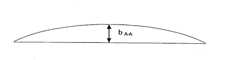
본 발명의 실시예에 따라서, 서셉터 플레이트는 서셉터 플레이트가 서셉터 플레이트 홀더내에 위치하고 웨이퍼가 서셉터 플레이트 위에 장착될 때 예상되는 굽힘의 반대 방향으로 어느 정도 미리 굽혀져 있다. 300mm 직경과 0.7mm의 두께의 CVD SiC 플레이트를 예로 들자. A-A 방향으로, 도 5A에서 보여진 바와 같이, 서셉터 플레이트는 bA-A = 150㎛ 휘어짐에 대응하게 만곡의 볼록하게 올라온(convex-up) 반경으로 미리 굽혀져 있다. 서셉터 플레이트를 서셉터 플레이트 홀더에 위치시킨 후에, 그림 5B와 같이 자체 무게로 인해 휘어짐이 bA-A = 50 ㎛로 감소한다. 서셉터 플레이트에 웨이퍼를 장착시킨 후에 휘어짐은 25㎛보다 작게 된다.In accordance with an embodiment of the present invention, the susceptor plate is bent to some extent in the opposite direction of the bending expected when the susceptor plate is located in the susceptor plate holder and the wafer is mounted on the susceptor plate. Take CVD SiC plates 300 mm in diameter and 0.7 mm thick, for example. In the AA direction, as shown in FIG. 5A, the susceptor plate is pre-curved with a curved convex-up radius corresponding to the bAA = 150 μm deflection. After placing the susceptor plate in the susceptor plate holder, the warpage reduces due to its weight to bAA = 50 μm, as shown in Figure 5B. After mounting the wafer on the susceptor plate, the warpage becomes smaller than 25 mu m.
도 6A와 같이 B-B방향으로의 서셉터 플레이트의 휘어짐은 500㎛에 이른다. 서셉터 플레이트를 서셉터 플레이트 홀더에 위치시킨 후에, 도 6B와 같이 휘어짐이 150 ㎛가 된다. 또 다시 서셉터 플레이트에 웨이퍼를 장착시킨 후에 휘어짐은 크지 않다.As shown in Fig. 6A, the deflection of the susceptor plate in the B-B direction reaches 500 mu m. After placing the susceptor plate on the susceptor plate holder, the warpage becomes 150 mu m as shown in Fig. 6B. Again, the warpage is not large after mounting the wafer on the susceptor plate.
실리콘 웨이퍼와의 접촉물질로서, CVD SiC는 1300℃의 온도에서 실리콘 웨이퍼의 접착을 나타내지 않는 적당한 물질로 보인다. CVD SiC는 소결된(sintered) SiC 물질을 충분히 봉할 수(seal) 있을 정도로 충분한 두께로 소결된 SiC 물질위에 증착될 수 있다. 더욱 바람직하게는, 서셉터 플레이트는 이른바 프리스탠딩(free-standing) CVD SiC로 만들어 질 수 있다. 이것은 SiC 코팅이 초기에 지지물질(예를 들어, 그래파이트)을 제거시킬 수 있는 정도의 두께로 지지물질에 증착되는 것이며, 몰드의 운반에서의 러스트 왁스(lost wax)방법과 유사하다. 1990년 12월 18일에 발행된 미국특허 제 4,978,567호의 내용은 참조로서 본 발명에 결합된다. 서셉터 플레이트의 설계된 형상이 머시닝(machining)을 필요로 하면, 머시닝은 역으로 행해질 수 있다. 즉 CVD SiC 코팅의 증착전에 지지물질위에 행해지는 것인데 이렇게 함으로써 단단한 CVD SiC물질을 머시닝하는 것이 생략되거나 최소한으로 줄어들 수 있다. 선택적으로, CVD SiC는 평탄한 지지 물질위에 증착될 수 있으며 CVD SiC는 필요에 따라 머시닝될 수도 있다. 어는 경우든지 서셉터 플레이트의 지지표면은 그 표면에 존재하는 돌출부를 제거하기 위하여 SiC물질의 증착후에 연삭처리되어야 한다.As a contact material with the silicon wafer, CVD SiC appears to be a suitable material that does not exhibit adhesion of the silicon wafer at a temperature of 1300 ° C. CVD SiC may be deposited on the sintered SiC material to a thickness sufficient to seal the sintered SiC material sufficiently. More preferably, the susceptor plate can be made of so-called free-standing CVD SiC. This is a SiC coating initially deposited on the support material to a thickness sufficient to remove the support material (eg graphite), similar to the method of lost wax in the delivery of the mold. The contents of U.S. Patent No. 4,978,567, issued December 18, 1990, are incorporated herein by reference. If the designed shape of the susceptor plate requires machining, the machining can be done in reverse. That is, on the support material prior to the deposition of the CVD SiC coating, whereby machining the hard CVD SiC material can be omitted or minimized. Optionally, CVD SiC may be deposited on a flat support material and the CVD SiC may be machined as needed. In either case, the support surface of the susceptor plate should be ground after deposition of the SiC material to remove protrusions present on the surface.
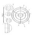
서셉터 플레이트의 제 1실시예는 도 7에 나와 있다. 서셉터 플레이트(100)는 웨이퍼 직경보다 조금 큰 직경을 갖는다. 웨이퍼를 지지하기 위한 지지 표면(110)은 충분히 평탄하다. 서셉터 플레이트(100)의 주변에는 올라간 숄더(shoulder)나 모서리(120)가 제공되어 있다. 열을 가하는 동안에, 올라간 모서리는 웨이퍼 모서리의 과열을 피하게 하고 가열동안 웨이퍼 모서리가 과도한 열 방사를 못하도록 막아준다. 식히는 동안에, 올라간 모서리는 웨이퍼가 너무 빨리 냉각되는 것을 막아준다. 또한, 올라간 모서리는 웨이퍼를 장착한 서셉터 플레이트(100)의 운반중에 웨이퍼가 수평방향으로 움직이는 것을 방지한다. 서셉터 플레이트(100)에는 자동 장착을 용이하게 하기 위하여 3개의 관통공(130)이 제공되어 있다. 관통공은 첫번째 방향의 최소크기는 약 5mm이고 첫번째 방향과 수직인 두번째 방향의 최대크기는 약 6mm인 타원형이다. 서셉터 플레이트(100)의 개략적 단면도는, 스케일에 맞지는 않지만, 도 8에 나와 있으며 지지표면에 수직의 크기는 명확히 하기 위하여 확대되어 있다. 본 발명의 목적을 위하여는, 서셉터 플레이트의 아래쪽 표면의 형상은 중요하지 않다. 중앙의 함몰부(140)의 기능은 2002년 5월 2일자 미국 가출원 제 60/377,904호 "2단계 엔드 이펙터(TWO-LEVEL END EFFECTOR)"에 자세히 설명되어 있다.A first embodiment of the susceptor plate is shown in FIG. The
서셉터 플레이트의 제 2실시예가 도 9에 나와 있다. 비슷한 부분은 도 7과 유사한 참조번호로 표시되어 있다. 이 실시예에서, 지지표면(110)은 홈(150)이 제 공되어 있다. 홈은 5mm폭에 0.2mm 깊이이다. 홈(150)은 웨이퍼를 서셉터 플레이트에 장착하기 위해 서셉터 플레이트가 웨이퍼로 움직이거나 그 반대인 때 웨이퍼와 서셉터 플레이트와의 사이에 있는 공기의 배출을 쉽게 해준다. 더욱 중요하게는, 홈(150)은 처리후에 웨이퍼가 서셉터 플레이트에서 분리될 때 웨이퍼와 서셉터 플레이트사이의 공기의 유입을 용이하게 한다. 도 9에서와 같이, 홈(150)내에 리프트 핀홀(130)을 위치시키는 것은 매우 효과적으로 보인다. 지지 표면(110)에 대한 평탄도의 요구는 이 서셉터 플레이트에도 여전히 적용될 수 있다. 관통공과 마찬가지로, 홈이 최소한의 크기라면 홈은 지지 표면 부분이 아니라는 것은 본 발명에 비추어 당업자에게는 명확할 것이다.A second embodiment of the susceptor plate is shown in FIG. Similar parts are designated by like reference numerals similar to FIG. 7. In this embodiment, the
도 10에 서셉터 플레이트의 제 3실시예가 나타나 있다. 비슷한 부분은 도 7과 유사한 참조번호로 표시되어 있다. 이 실시예의 지지표면(110)은 올라간 페데스탈(pedestal, 160)을 포함한다. 이웃하는 페데스탈(160)의 거리는 7mm이다. 페데스탈의 크기는 1×1mm이고 높이는 0.2mm이다. 지지표면은 조합된 페데스탈의 상부 표면으로 구성되며 평탄도의 요구는 이 불연속적인 상부 표면에도 적용된다. 0.1×0.1mm크기의 페데스탈은 페데스탈들이 과도하게 떨어져 있지만 않다면, 응력 집중에 의한 웨이퍼 손상을 막기 위한 충분한 지지 영역을 제공한다는 것이 밝혀졌다.A third embodiment of a susceptor plate is shown in FIG. Similar parts are designated by like reference numerals similar to FIG. 7. The
당업자라면 본 발명의 범위를 벗어나지 않고 위에서 설명한 공정에 여러가지 생략, 추가, 변형이 가해질 수 있는 것을 이해할 것이다. 예를 들어, 여기에서 설명된 운반 스테이션(transshipment station)은 개방된 카세트에서 제공될 수 있거 나 카세트와 연관되지 않은 분리된 스테이션에서 제공될 수 있다. 또한, 다른 배치에서, 탈착중에 웨이퍼를 지지 플레이트에서 분리하는 메카니즘이나 장착중에 웨이퍼를 지지 플레이트에 결합시키는 것은 다른 구조를 취할 수 있다. 모든 이러한 변형과 변화는 첨부되는 청구범위에서 정의된 바와 같이 본 발명의 범위내에 있도록 의도되어 있다.Those skilled in the art will appreciate that various omissions, additions, and variations may be made to the processes described above without departing from the scope of the present invention. For example, the delivery station described herein may be provided in an open cassette or may be provided in a separate station that is not associated with a cassette. Also, in other arrangements, the mechanism of separating the wafer from the support plate during desorption or joining the wafer to the support plate during mounting may take a different structure. All such modifications and variations are intended to be within the scope of the invention as defined in the appended claims.
본 발명에 의하면, 300mm 웨이퍼를 1000℃이상의 온도에서, 웨이퍼가 자동으로 다루어지면서 웨이퍼의 소성변형이 최소화되거나 제거된다.According to the present invention, the 300mm wafer at a temperature of 1000 ° C. or more, the wafer is automatically handled and plastic deformation of the wafer is minimized or eliminated.
Claims (29)
Translated fromKoreanApplications Claiming Priority (2)
| Application Number | Priority Date | Filing Date | Title |
|---|---|---|---|
| US40784202P | 2002-08-30 | 2002-08-30 | |
| US60/407,842 | 2002-08-30 |
Publications (2)
| Publication Number | Publication Date |
|---|---|
| KR20040020023A KR20040020023A (en) | 2004-03-06 |
| KR101018850B1true KR101018850B1 (en) | 2011-03-04 |
Family
ID=32298234
Family Applications (1)
| Application Number | Title | Priority Date | Filing Date |
|---|---|---|---|
| KR1020030060106AExpired - LifetimeKR101018850B1 (en) | 2002-08-30 | 2003-08-29 | Susceptor Plates for High Temperature Heat Treatment |
Country Status (3)
| Country | Link |
|---|---|
| US (1) | US7256375B2 (en) |
| JP (1) | JP2004134761A (en) |
| KR (1) | KR101018850B1 (en) |
Families Citing this family (323)
| Publication number | Priority date | Publication date | Assignee | Title |
|---|---|---|---|---|
| CN100517612C (en)* | 2003-04-02 | 2009-07-22 | 株式会社上睦可 | Heat Treatment Fixtures for Semiconductor Wafers |
| EP1670534B1 (en)* | 2003-07-02 | 2010-01-27 | Cook Incorporated | Coaxial Catheters |
| US7181132B2 (en) | 2003-08-20 | 2007-02-20 | Asm International N.V. | Method and system for loading substrate supports into a substrate holder |
| JP4534619B2 (en)* | 2004-06-21 | 2010-09-01 | 株式会社Sumco | Heat treatment jig for semiconductor silicon substrate |
| KR100841196B1 (en)* | 2004-06-21 | 2008-06-24 | 가부시키가이샤 섬코 | Heat Treatment Jig for Semiconductor Silicon Substrate |
| US20060060145A1 (en) | 2004-09-17 | 2006-03-23 | Van Den Berg Jannes R | Susceptor with surface roughness for high temperature substrate processing |
| DE102005013831B4 (en)* | 2005-03-24 | 2008-10-16 | Siltronic Ag | Silicon wafer and method for the thermal treatment of a silicon wafer |
| TWI327761B (en)* | 2005-10-07 | 2010-07-21 | Rohm & Haas Elect Mat | Method for making semiconductor wafer and wafer holding article |
| KR100684359B1 (en)* | 2005-11-28 | 2007-02-20 | 주식회사 유진테크 | Susceptor strain relief |
| JP5065660B2 (en)* | 2005-12-02 | 2012-11-07 | ローム・アンド・ハース・エレクトロニック・マテリアルズ,エル.エル.シー. | Semiconductor processing |
| JP5205738B2 (en)* | 2006-10-16 | 2013-06-05 | 株式会社Sumco | Silicon wafer support method, heat treatment jig and heat treatment wafer |
| ATE513311T1 (en)* | 2006-11-10 | 2011-07-15 | Saint Gobain Ceramics | SUSSCEPTOR AND METHOD FOR PRODUCING AN LED DEVICE USING THIS SUSSCEPTOR |
| TWI547999B (en)* | 2007-09-17 | 2016-09-01 | Dsgi公司 | System for and method of microwave annealing semiconductor material |
| US8042697B2 (en)* | 2008-06-30 | 2011-10-25 | Memc Electronic Materials, Inc. | Low thermal mass semiconductor wafer support |
| US9394608B2 (en) | 2009-04-06 | 2016-07-19 | Asm America, Inc. | Semiconductor processing reactor and components thereof |
| US8802201B2 (en) | 2009-08-14 | 2014-08-12 | Asm America, Inc. | Systems and methods for thin-film deposition of metal oxides using excited nitrogen-oxygen species |
| US20130023129A1 (en) | 2011-07-20 | 2013-01-24 | Asm America, Inc. | Pressure transmitter for a semiconductor processing environment |
| TWI505400B (en)* | 2011-08-26 | 2015-10-21 | Lg Siltron Inc | Susceptor |
| TWI541928B (en)* | 2011-10-14 | 2016-07-11 | 晶元光電股份有限公司 | Wafer carrier |
| US9017481B1 (en) | 2011-10-28 | 2015-04-28 | Asm America, Inc. | Process feed management for semiconductor substrate processing |
| US10316412B2 (en) | 2012-04-18 | 2019-06-11 | Veeco Instruments Inc. | Wafter carrier for chemical vapor deposition systems |
| US8865602B2 (en) | 2012-09-28 | 2014-10-21 | Applied Materials, Inc. | Edge ring lip |
| US10714315B2 (en) | 2012-10-12 | 2020-07-14 | Asm Ip Holdings B.V. | Semiconductor reaction chamber showerhead |
| CN104704626B (en) | 2012-10-24 | 2017-12-05 | 应用材料公司 | Minimal contact edge ring for rapid heat treatment |
| US20160376700A1 (en) | 2013-02-01 | 2016-12-29 | Asm Ip Holding B.V. | System for treatment of deposition reactor |
| US10167571B2 (en) | 2013-03-15 | 2019-01-01 | Veeco Instruments Inc. | Wafer carrier having provisions for improving heating uniformity in chemical vapor deposition systems |
| US10047457B2 (en)* | 2013-09-16 | 2018-08-14 | Applied Materials, Inc. | EPI pre-heat ring |
| US11015245B2 (en) | 2014-03-19 | 2021-05-25 | Asm Ip Holding B.V. | Gas-phase reactor and system having exhaust plenum and components thereof |
| US10858737B2 (en) | 2014-07-28 | 2020-12-08 | Asm Ip Holding B.V. | Showerhead assembly and components thereof |
| US9890456B2 (en) | 2014-08-21 | 2018-02-13 | Asm Ip Holding B.V. | Method and system for in situ formation of gas-phase compounds |
| CN105369348B (en)* | 2014-08-29 | 2017-12-12 | 中微半导体设备(上海)有限公司 | A kind of wafer carrier for MOCVD reaction systems |
| US10941490B2 (en) | 2014-10-07 | 2021-03-09 | Asm Ip Holding B.V. | Multiple temperature range susceptor, assembly, reactor and system including the susceptor, and methods of using the same |
| US10276355B2 (en) | 2015-03-12 | 2019-04-30 | Asm Ip Holding B.V. | Multi-zone reactor, system including the reactor, and method of using the same |
| US10458018B2 (en) | 2015-06-26 | 2019-10-29 | Asm Ip Holding B.V. | Structures including metal carbide material, devices including the structures, and methods of forming same |
| US10211308B2 (en) | 2015-10-21 | 2019-02-19 | Asm Ip Holding B.V. | NbMC layers |
| US20170175265A1 (en)* | 2015-12-18 | 2017-06-22 | Applied Materials, Inc. | Flat susceptor with grooves for minimizing temperature profile across a substrate |
| US11139308B2 (en) | 2015-12-29 | 2021-10-05 | Asm Ip Holding B.V. | Atomic layer deposition of III-V compounds to form V-NAND devices |
| US10529554B2 (en) | 2016-02-19 | 2020-01-07 | Asm Ip Holding B.V. | Method for forming silicon nitride film selectively on sidewalls or flat surfaces of trenches |
| US10343920B2 (en) | 2016-03-18 | 2019-07-09 | Asm Ip Holding B.V. | Aligned carbon nanotubes |
| US10190213B2 (en) | 2016-04-21 | 2019-01-29 | Asm Ip Holding B.V. | Deposition of metal borides |
| US10865475B2 (en) | 2016-04-21 | 2020-12-15 | Asm Ip Holding B.V. | Deposition of metal borides and silicides |
| US10367080B2 (en) | 2016-05-02 | 2019-07-30 | Asm Ip Holding B.V. | Method of forming a germanium oxynitride film |
| US11453943B2 (en) | 2016-05-25 | 2022-09-27 | Asm Ip Holding B.V. | Method for forming carbon-containing silicon/metal oxide or nitride film by ALD using silicon precursor and hydrocarbon precursor |
| US9859151B1 (en) | 2016-07-08 | 2018-01-02 | Asm Ip Holding B.V. | Selective film deposition method to form air gaps |
| US10612137B2 (en) | 2016-07-08 | 2020-04-07 | Asm Ip Holdings B.V. | Organic reactants for atomic layer deposition |
| US9812320B1 (en) | 2016-07-28 | 2017-11-07 | Asm Ip Holding B.V. | Method and apparatus for filling a gap |
| US9887082B1 (en) | 2016-07-28 | 2018-02-06 | Asm Ip Holding B.V. | Method and apparatus for filling a gap |
| KR102532607B1 (en) | 2016-07-28 | 2023-05-15 | 에이에스엠 아이피 홀딩 비.브이. | Substrate processing apparatus and method of operating the same |
| US10643826B2 (en) | 2016-10-26 | 2020-05-05 | Asm Ip Holdings B.V. | Methods for thermally calibrating reaction chambers |
| US11532757B2 (en) | 2016-10-27 | 2022-12-20 | Asm Ip Holding B.V. | Deposition of charge trapping layers |
| US10714350B2 (en) | 2016-11-01 | 2020-07-14 | ASM IP Holdings, B.V. | Methods for forming a transition metal niobium nitride film on a substrate by atomic layer deposition and related semiconductor device structures |
| US10229833B2 (en) | 2016-11-01 | 2019-03-12 | Asm Ip Holding B.V. | Methods for forming a transition metal nitride film on a substrate by atomic layer deposition and related semiconductor device structures |
| KR102546317B1 (en) | 2016-11-15 | 2023-06-21 | 에이에스엠 아이피 홀딩 비.브이. | Gas supply unit and substrate processing apparatus including the same |
| KR102762543B1 (en) | 2016-12-14 | 2025-02-05 | 에이에스엠 아이피 홀딩 비.브이. | Substrate processing apparatus |
| US11581186B2 (en) | 2016-12-15 | 2023-02-14 | Asm Ip Holding B.V. | Sequential infiltration synthesis apparatus |
| US11447861B2 (en) | 2016-12-15 | 2022-09-20 | Asm Ip Holding B.V. | Sequential infiltration synthesis apparatus and a method of forming a patterned structure |
| KR102700194B1 (en) | 2016-12-19 | 2024-08-28 | 에이에스엠 아이피 홀딩 비.브이. | Substrate processing apparatus |
| US10269558B2 (en) | 2016-12-22 | 2019-04-23 | Asm Ip Holding B.V. | Method of forming a structure on a substrate |
| US10867788B2 (en) | 2016-12-28 | 2020-12-15 | Asm Ip Holding B.V. | Method of forming a structure on a substrate |
| US11390950B2 (en) | 2017-01-10 | 2022-07-19 | Asm Ip Holding B.V. | Reactor system and method to reduce residue buildup during a film deposition process |
| US10468261B2 (en) | 2017-02-15 | 2019-11-05 | Asm Ip Holding B.V. | Methods for forming a metallic film on a substrate by cyclical deposition and related semiconductor device structures |
| US10529563B2 (en) | 2017-03-29 | 2020-01-07 | Asm Ip Holdings B.V. | Method for forming doped metal oxide films on a substrate by cyclical deposition and related semiconductor device structures |
| KR102457289B1 (en) | 2017-04-25 | 2022-10-21 | 에이에스엠 아이피 홀딩 비.브이. | Method for depositing a thin film and manufacturing a semiconductor device |
| US10770286B2 (en) | 2017-05-08 | 2020-09-08 | Asm Ip Holdings B.V. | Methods for selectively forming a silicon nitride film on a substrate and related semiconductor device structures |
| US10892156B2 (en) | 2017-05-08 | 2021-01-12 | Asm Ip Holding B.V. | Methods for forming a silicon nitride film on a substrate and related semiconductor device structures |
| US10886123B2 (en) | 2017-06-02 | 2021-01-05 | Asm Ip Holding B.V. | Methods for forming low temperature semiconductor layers and related semiconductor device structures |
| US12040200B2 (en) | 2017-06-20 | 2024-07-16 | Asm Ip Holding B.V. | Semiconductor processing apparatus and methods for calibrating a semiconductor processing apparatus |
| US11306395B2 (en) | 2017-06-28 | 2022-04-19 | Asm Ip Holding B.V. | Methods for depositing a transition metal nitride film on a substrate by atomic layer deposition and related deposition apparatus |
| KR20190009245A (en) | 2017-07-18 | 2019-01-28 | 에이에스엠 아이피 홀딩 비.브이. | Methods for forming a semiconductor device structure and related semiconductor device structures |
| US10541333B2 (en) | 2017-07-19 | 2020-01-21 | Asm Ip Holding B.V. | Method for depositing a group IV semiconductor and related semiconductor device structures |
| US11374112B2 (en) | 2017-07-19 | 2022-06-28 | Asm Ip Holding B.V. | Method for depositing a group IV semiconductor and related semiconductor device structures |
| US11018002B2 (en) | 2017-07-19 | 2021-05-25 | Asm Ip Holding B.V. | Method for selectively depositing a Group IV semiconductor and related semiconductor device structures |
| US10590535B2 (en) | 2017-07-26 | 2020-03-17 | Asm Ip Holdings B.V. | Chemical treatment, deposition and/or infiltration apparatus and method for using the same |
| TWI815813B (en) | 2017-08-04 | 2023-09-21 | 荷蘭商Asm智慧財產控股公司 | Showerhead assembly for distributing a gas within a reaction chamber |
| US10692741B2 (en) | 2017-08-08 | 2020-06-23 | Asm Ip Holdings B.V. | Radiation shield |
| US10770336B2 (en) | 2017-08-08 | 2020-09-08 | Asm Ip Holding B.V. | Substrate lift mechanism and reactor including same |
| US11769682B2 (en) | 2017-08-09 | 2023-09-26 | Asm Ip Holding B.V. | Storage apparatus for storing cassettes for substrates and processing apparatus equipped therewith |
| US11139191B2 (en) | 2017-08-09 | 2021-10-05 | Asm Ip Holding B.V. | Storage apparatus for storing cassettes for substrates and processing apparatus equipped therewith |
| US11830730B2 (en) | 2017-08-29 | 2023-11-28 | Asm Ip Holding B.V. | Layer forming method and apparatus |
| US11295980B2 (en) | 2017-08-30 | 2022-04-05 | Asm Ip Holding B.V. | Methods for depositing a molybdenum metal film over a dielectric surface of a substrate by a cyclical deposition process and related semiconductor device structures |
| KR102491945B1 (en) | 2017-08-30 | 2023-01-26 | 에이에스엠 아이피 홀딩 비.브이. | Substrate processing apparatus |
| US11056344B2 (en) | 2017-08-30 | 2021-07-06 | Asm Ip Holding B.V. | Layer forming method |
| KR102401446B1 (en) | 2017-08-31 | 2022-05-24 | 에이에스엠 아이피 홀딩 비.브이. | Substrate processing apparatus |
| KR102630301B1 (en) | 2017-09-21 | 2024-01-29 | 에이에스엠 아이피 홀딩 비.브이. | Method of sequential infiltration synthesis treatment of infiltrateable material and structures and devices formed using same |
| US10844484B2 (en) | 2017-09-22 | 2020-11-24 | Asm Ip Holding B.V. | Apparatus for dispensing a vapor phase reactant to a reaction chamber and related methods |
| US10658205B2 (en) | 2017-09-28 | 2020-05-19 | Asm Ip Holdings B.V. | Chemical dispensing apparatus and methods for dispensing a chemical to a reaction chamber |
| US10403504B2 (en) | 2017-10-05 | 2019-09-03 | Asm Ip Holding B.V. | Method for selectively depositing a metallic film on a substrate |
| US10923344B2 (en) | 2017-10-30 | 2021-02-16 | Asm Ip Holding B.V. | Methods for forming a semiconductor structure and related semiconductor structures |
| US10910262B2 (en) | 2017-11-16 | 2021-02-02 | Asm Ip Holding B.V. | Method of selectively depositing a capping layer structure on a semiconductor device structure |
| US11022879B2 (en) | 2017-11-24 | 2021-06-01 | Asm Ip Holding B.V. | Method of forming an enhanced unexposed photoresist layer |
| CN111344522B (en) | 2017-11-27 | 2022-04-12 | 阿斯莫Ip控股公司 | Including clean mini-environment device |
| WO2019103613A1 (en) | 2017-11-27 | 2019-05-31 | Asm Ip Holding B.V. | A storage device for storing wafer cassettes for use with a batch furnace |
| US10872771B2 (en) | 2018-01-16 | 2020-12-22 | Asm Ip Holding B. V. | Method for depositing a material film on a substrate within a reaction chamber by a cyclical deposition process and related device structures |
| TWI799494B (en) | 2018-01-19 | 2023-04-21 | 荷蘭商Asm 智慧財產控股公司 | Deposition method |
| KR102695659B1 (en) | 2018-01-19 | 2024-08-14 | 에이에스엠 아이피 홀딩 비.브이. | Method for depositing a gap filling layer by plasma assisted deposition |
| US11018047B2 (en) | 2018-01-25 | 2021-05-25 | Asm Ip Holding B.V. | Hybrid lift pin |
| USD880437S1 (en) | 2018-02-01 | 2020-04-07 | Asm Ip Holding B.V. | Gas supply plate for semiconductor manufacturing apparatus |
| US11081345B2 (en) | 2018-02-06 | 2021-08-03 | Asm Ip Holding B.V. | Method of post-deposition treatment for silicon oxide film |
| US10896820B2 (en) | 2018-02-14 | 2021-01-19 | Asm Ip Holding B.V. | Method for depositing a ruthenium-containing film on a substrate by a cyclical deposition process |
| WO2019158960A1 (en) | 2018-02-14 | 2019-08-22 | Asm Ip Holding B.V. | A method for depositing a ruthenium-containing film on a substrate by a cyclical deposition process |
| US10731249B2 (en) | 2018-02-15 | 2020-08-04 | Asm Ip Holding B.V. | Method of forming a transition metal containing film on a substrate by a cyclical deposition process, a method for supplying a transition metal halide compound to a reaction chamber, and related vapor deposition apparatus |
| KR102636427B1 (en) | 2018-02-20 | 2024-02-13 | 에이에스엠 아이피 홀딩 비.브이. | Substrate processing method and apparatus |
| US10975470B2 (en) | 2018-02-23 | 2021-04-13 | Asm Ip Holding B.V. | Apparatus for detecting or monitoring for a chemical precursor in a high temperature environment |
| US11473195B2 (en) | 2018-03-01 | 2022-10-18 | Asm Ip Holding B.V. | Semiconductor processing apparatus and a method for processing a substrate |
| US11629406B2 (en) | 2018-03-09 | 2023-04-18 | Asm Ip Holding B.V. | Semiconductor processing apparatus comprising one or more pyrometers for measuring a temperature of a substrate during transfer of the substrate |
| US11114283B2 (en) | 2018-03-16 | 2021-09-07 | Asm Ip Holding B.V. | Reactor, system including the reactor, and methods of manufacturing and using same |
| KR102646467B1 (en) | 2018-03-27 | 2024-03-11 | 에이에스엠 아이피 홀딩 비.브이. | Method of forming an electrode on a substrate and a semiconductor device structure including an electrode |
| US11230766B2 (en) | 2018-03-29 | 2022-01-25 | Asm Ip Holding B.V. | Substrate processing apparatus and method |
| US11088002B2 (en) | 2018-03-29 | 2021-08-10 | Asm Ip Holding B.V. | Substrate rack and a substrate processing system and method |
| KR102501472B1 (en) | 2018-03-30 | 2023-02-20 | 에이에스엠 아이피 홀딩 비.브이. | Substrate processing method |
| KR102600229B1 (en) | 2018-04-09 | 2023-11-10 | 에이에스엠 아이피 홀딩 비.브이. | Substrate supporting device, substrate processing apparatus including the same and substrate processing method |
| TWI811348B (en) | 2018-05-08 | 2023-08-11 | 荷蘭商Asm 智慧財產控股公司 | Methods for depositing an oxide film on a substrate by a cyclical deposition process and related device structures |
| US12025484B2 (en) | 2018-05-08 | 2024-07-02 | Asm Ip Holding B.V. | Thin film forming method |
| US12272527B2 (en) | 2018-05-09 | 2025-04-08 | Asm Ip Holding B.V. | Apparatus for use with hydrogen radicals and method of using same |
| KR20190129718A (en) | 2018-05-11 | 2019-11-20 | 에이에스엠 아이피 홀딩 비.브이. | Methods for forming a doped metal carbide film on a substrate and related semiconductor device structures |
| KR102596988B1 (en) | 2018-05-28 | 2023-10-31 | 에이에스엠 아이피 홀딩 비.브이. | Method of processing a substrate and a device manufactured by the same |
| US11718913B2 (en) | 2018-06-04 | 2023-08-08 | Asm Ip Holding B.V. | Gas distribution system and reactor system including same |
| TWI840362B (en) | 2018-06-04 | 2024-05-01 | 荷蘭商Asm Ip私人控股有限公司 | Wafer handling chamber with moisture reduction |
| US11286562B2 (en) | 2018-06-08 | 2022-03-29 | Asm Ip Holding B.V. | Gas-phase chemical reactor and method of using same |
| US10797133B2 (en) | 2018-06-21 | 2020-10-06 | Asm Ip Holding B.V. | Method for depositing a phosphorus doped silicon arsenide film and related semiconductor device structures |
| KR102568797B1 (en) | 2018-06-21 | 2023-08-21 | 에이에스엠 아이피 홀딩 비.브이. | Substrate processing system |
| KR102854019B1 (en) | 2018-06-27 | 2025-09-02 | 에이에스엠 아이피 홀딩 비.브이. | Periodic deposition method for forming a metal-containing material and films and structures comprising the metal-containing material |
| TWI873894B (en) | 2018-06-27 | 2025-02-21 | 荷蘭商Asm Ip私人控股有限公司 | Cyclic deposition methods for forming metal-containing material and films and structures including the metal-containing material |
| US10612136B2 (en) | 2018-06-29 | 2020-04-07 | ASM IP Holding, B.V. | Temperature-controlled flange and reactor system including same |
| KR102686758B1 (en) | 2018-06-29 | 2024-07-18 | 에이에스엠 아이피 홀딩 비.브이. | Method for depositing a thin film and manufacturing a semiconductor device |
| US10388513B1 (en) | 2018-07-03 | 2019-08-20 | Asm Ip Holding B.V. | Method for depositing silicon-free carbon-containing film as gap-fill layer by pulse plasma-assisted deposition |
| US10755922B2 (en) | 2018-07-03 | 2020-08-25 | Asm Ip Holding B.V. | Method for depositing silicon-free carbon-containing film as gap-fill layer by pulse plasma-assisted deposition |
| US10767789B2 (en) | 2018-07-16 | 2020-09-08 | Asm Ip Holding B.V. | Diaphragm valves, valve components, and methods for forming valve components |
| US11053591B2 (en) | 2018-08-06 | 2021-07-06 | Asm Ip Holding B.V. | Multi-port gas injection system and reactor system including same |
| US10883175B2 (en) | 2018-08-09 | 2021-01-05 | Asm Ip Holding B.V. | Vertical furnace for processing substrates and a liner for use therein |
| US10829852B2 (en) | 2018-08-16 | 2020-11-10 | Asm Ip Holding B.V. | Gas distribution device for a wafer processing apparatus |
| US11430674B2 (en) | 2018-08-22 | 2022-08-30 | Asm Ip Holding B.V. | Sensor array, apparatus for dispensing a vapor phase reactant to a reaction chamber and related methods |
| US11024523B2 (en) | 2018-09-11 | 2021-06-01 | Asm Ip Holding B.V. | Substrate processing apparatus and method |
| KR102707956B1 (en) | 2018-09-11 | 2024-09-19 | 에이에스엠 아이피 홀딩 비.브이. | Method for deposition of a thin film |
| US11049751B2 (en) | 2018-09-14 | 2021-06-29 | Asm Ip Holding B.V. | Cassette supply system to store and handle cassettes and processing apparatus equipped therewith |
| CN110970344B (en) | 2018-10-01 | 2024-10-25 | Asmip控股有限公司 | Substrate holding apparatus, system comprising the same and method of using the same |
| US11232963B2 (en) | 2018-10-03 | 2022-01-25 | Asm Ip Holding B.V. | Substrate processing apparatus and method |
| KR102592699B1 (en) | 2018-10-08 | 2023-10-23 | 에이에스엠 아이피 홀딩 비.브이. | Substrate support unit and apparatuses for depositing thin film and processing the substrate including the same |
| KR102605121B1 (en) | 2018-10-19 | 2023-11-23 | 에이에스엠 아이피 홀딩 비.브이. | Substrate processing apparatus and substrate processing method |
| KR102546322B1 (en) | 2018-10-19 | 2023-06-21 | 에이에스엠 아이피 홀딩 비.브이. | Substrate processing apparatus and substrate processing method |
| USD948463S1 (en) | 2018-10-24 | 2022-04-12 | Asm Ip Holding B.V. | Susceptor for semiconductor substrate supporting apparatus |
| US12378665B2 (en) | 2018-10-26 | 2025-08-05 | Asm Ip Holding B.V. | High temperature coatings for a preclean and etch apparatus and related methods |
| US11087997B2 (en) | 2018-10-31 | 2021-08-10 | Asm Ip Holding B.V. | Substrate processing apparatus for processing substrates |
| KR102748291B1 (en) | 2018-11-02 | 2024-12-31 | 에이에스엠 아이피 홀딩 비.브이. | Substrate support unit and substrate processing apparatus including the same |
| US11572620B2 (en) | 2018-11-06 | 2023-02-07 | Asm Ip Holding B.V. | Methods for selectively depositing an amorphous silicon film on a substrate |
| US11031242B2 (en) | 2018-11-07 | 2021-06-08 | Asm Ip Holding B.V. | Methods for depositing a boron doped silicon germanium film |
| US10818758B2 (en) | 2018-11-16 | 2020-10-27 | Asm Ip Holding B.V. | Methods for forming a metal silicate film on a substrate in a reaction chamber and related semiconductor device structures |
| US10847366B2 (en) | 2018-11-16 | 2020-11-24 | Asm Ip Holding B.V. | Methods for depositing a transition metal chalcogenide film on a substrate by a cyclical deposition process |
| US12040199B2 (en) | 2018-11-28 | 2024-07-16 | Asm Ip Holding B.V. | Substrate processing apparatus for processing substrates |
| US11217444B2 (en) | 2018-11-30 | 2022-01-04 | Asm Ip Holding B.V. | Method for forming an ultraviolet radiation responsive metal oxide-containing film |
| KR102636428B1 (en) | 2018-12-04 | 2024-02-13 | 에이에스엠 아이피 홀딩 비.브이. | A method for cleaning a substrate processing apparatus |
| US11158513B2 (en) | 2018-12-13 | 2021-10-26 | Asm Ip Holding B.V. | Methods for forming a rhenium-containing film on a substrate by a cyclical deposition process and related semiconductor device structures |
| TWI874340B (en) | 2018-12-14 | 2025-03-01 | 荷蘭商Asm Ip私人控股有限公司 | Method of forming device structure, structure formed by the method and system for performing the method |
| TWI866480B (en) | 2019-01-17 | 2024-12-11 | 荷蘭商Asm Ip 私人控股有限公司 | Methods of forming a transition metal containing film on a substrate by a cyclical deposition process |
| KR102727227B1 (en) | 2019-01-22 | 2024-11-07 | 에이에스엠 아이피 홀딩 비.브이. | Semiconductor processing device |
| CN111524788B (en) | 2019-02-01 | 2023-11-24 | Asm Ip私人控股有限公司 | Method for forming topologically selective films of silicon oxide |
| TWI873122B (en) | 2019-02-20 | 2025-02-21 | 荷蘭商Asm Ip私人控股有限公司 | Method of filling a recess formed within a surface of a substrate, semiconductor structure formed according to the method, and semiconductor processing apparatus |
| TWI838458B (en) | 2019-02-20 | 2024-04-11 | 荷蘭商Asm Ip私人控股有限公司 | Apparatus and methods for plug fill deposition in 3-d nand applications |
| TWI845607B (en) | 2019-02-20 | 2024-06-21 | 荷蘭商Asm Ip私人控股有限公司 | Cyclical deposition method and apparatus for filling a recess formed within a substrate surface |
| KR102626263B1 (en) | 2019-02-20 | 2024-01-16 | 에이에스엠 아이피 홀딩 비.브이. | Cyclical deposition method including treatment step and apparatus for same |
| TWI842826B (en) | 2019-02-22 | 2024-05-21 | 荷蘭商Asm Ip私人控股有限公司 | Substrate processing apparatus and method for processing substrate |
| KR102782593B1 (en) | 2019-03-08 | 2025-03-14 | 에이에스엠 아이피 홀딩 비.브이. | Structure Including SiOC Layer and Method of Forming Same |
| US11742198B2 (en) | 2019-03-08 | 2023-08-29 | Asm Ip Holding B.V. | Structure including SiOCN layer and method of forming same |
| KR102858005B1 (en) | 2019-03-08 | 2025-09-09 | 에이에스엠 아이피 홀딩 비.브이. | Method for Selective Deposition of Silicon Nitride Layer and Structure Including Selectively-Deposited Silicon Nitride Layer |
| JP2020167398A (en) | 2019-03-28 | 2020-10-08 | エーエスエム・アイピー・ホールディング・ベー・フェー | Door openers and substrate processing equipment provided with door openers |
| KR102809999B1 (en) | 2019-04-01 | 2025-05-19 | 에이에스엠 아이피 홀딩 비.브이. | Method of manufacturing semiconductor device |
| KR20200123380A (en) | 2019-04-19 | 2020-10-29 | 에이에스엠 아이피 홀딩 비.브이. | Layer forming method and apparatus |
| KR20200125453A (en) | 2019-04-24 | 2020-11-04 | 에이에스엠 아이피 홀딩 비.브이. | Gas-phase reactor system and method of using same |
| US11289326B2 (en) | 2019-05-07 | 2022-03-29 | Asm Ip Holding B.V. | Method for reforming amorphous carbon polymer film |
| KR20200130121A (en) | 2019-05-07 | 2020-11-18 | 에이에스엠 아이피 홀딩 비.브이. | Chemical source vessel with dip tube |
| KR20200130652A (en) | 2019-05-10 | 2020-11-19 | 에이에스엠 아이피 홀딩 비.브이. | Method of depositing material onto a surface and structure formed according to the method |
| JP7612342B2 (en) | 2019-05-16 | 2025-01-14 | エーエスエム・アイピー・ホールディング・ベー・フェー | Wafer boat handling apparatus, vertical batch furnace and method |
| JP7598201B2 (en) | 2019-05-16 | 2024-12-11 | エーエスエム・アイピー・ホールディング・ベー・フェー | Wafer boat handling apparatus, vertical batch furnace and method |
| USD975665S1 (en) | 2019-05-17 | 2023-01-17 | Asm Ip Holding B.V. | Susceptor shaft |
| USD947913S1 (en) | 2019-05-17 | 2022-04-05 | Asm Ip Holding B.V. | Susceptor shaft |
| DE102019207433A1 (en)* | 2019-05-21 | 2020-11-26 | Siltronic Ag | Process for the production of semiconductor wafers |
| USD935572S1 (en) | 2019-05-24 | 2021-11-09 | Asm Ip Holding B.V. | Gas channel plate |
| USD922229S1 (en) | 2019-06-05 | 2021-06-15 | Asm Ip Holding B.V. | Device for controlling a temperature of a gas supply unit |
| KR20200141002A (en) | 2019-06-06 | 2020-12-17 | 에이에스엠 아이피 홀딩 비.브이. | Method of using a gas-phase reactor system including analyzing exhausted gas |
| KR20200141931A (en) | 2019-06-10 | 2020-12-21 | 에이에스엠 아이피 홀딩 비.브이. | Method for cleaning quartz epitaxial chambers |
| KR20200143254A (en) | 2019-06-11 | 2020-12-23 | 에이에스엠 아이피 홀딩 비.브이. | Method of forming an electronic structure using an reforming gas, system for performing the method, and structure formed using the method |
| USD944946S1 (en) | 2019-06-14 | 2022-03-01 | Asm Ip Holding B.V. | Shower plate |
| USD931978S1 (en) | 2019-06-27 | 2021-09-28 | Asm Ip Holding B.V. | Showerhead vacuum transport |
| KR20210005515A (en) | 2019-07-03 | 2021-01-14 | 에이에스엠 아이피 홀딩 비.브이. | Temperature control assembly for substrate processing apparatus and method of using same |
| JP7499079B2 (en) | 2019-07-09 | 2024-06-13 | エーエスエム・アイピー・ホールディング・ベー・フェー | Plasma device using coaxial waveguide and substrate processing method |
| CN112216646A (en) | 2019-07-10 | 2021-01-12 | Asm Ip私人控股有限公司 | Substrate supporting assembly and substrate processing device comprising same |
| KR20210010307A (en) | 2019-07-16 | 2021-01-27 | 에이에스엠 아이피 홀딩 비.브이. | Substrate processing apparatus |
| KR20210010816A (en) | 2019-07-17 | 2021-01-28 | 에이에스엠 아이피 홀딩 비.브이. | Radical assist ignition plasma system and method |
| KR102860110B1 (en) | 2019-07-17 | 2025-09-16 | 에이에스엠 아이피 홀딩 비.브이. | Methods of forming silicon germanium structures |
| US11643724B2 (en) | 2019-07-18 | 2023-05-09 | Asm Ip Holding B.V. | Method of forming structures using a neutral beam |
| KR20210010817A (en) | 2019-07-19 | 2021-01-28 | 에이에스엠 아이피 홀딩 비.브이. | Method of Forming Topology-Controlled Amorphous Carbon Polymer Film |
| TWI839544B (en) | 2019-07-19 | 2024-04-21 | 荷蘭商Asm Ip私人控股有限公司 | Method of forming topology-controlled amorphous carbon polymer film |
| TWI851767B (en) | 2019-07-29 | 2024-08-11 | 荷蘭商Asm Ip私人控股有限公司 | Methods for selective deposition utilizing n-type dopants and/or alternative dopants to achieve high dopant incorporation |
| CN112309900A (en) | 2019-07-30 | 2021-02-02 | Asm Ip私人控股有限公司 | Substrate processing apparatus |
| CN112309899A (en) | 2019-07-30 | 2021-02-02 | Asm Ip私人控股有限公司 | Substrate processing apparatus |
| US12169361B2 (en) | 2019-07-30 | 2024-12-17 | Asm Ip Holding B.V. | Substrate processing apparatus and method |
| US11587815B2 (en) | 2019-07-31 | 2023-02-21 | Asm Ip Holding B.V. | Vertical batch furnace assembly |
| US11587814B2 (en) | 2019-07-31 | 2023-02-21 | Asm Ip Holding B.V. | Vertical batch furnace assembly |
| US11227782B2 (en) | 2019-07-31 | 2022-01-18 | Asm Ip Holding B.V. | Vertical batch furnace assembly |
| CN112323048B (en) | 2019-08-05 | 2024-02-09 | Asm Ip私人控股有限公司 | Liquid level sensor for chemical source container |
| CN112342526A (en) | 2019-08-09 | 2021-02-09 | Asm Ip私人控股有限公司 | Heater assembly including cooling device and method of using same |
| USD965044S1 (en) | 2019-08-19 | 2022-09-27 | Asm Ip Holding B.V. | Susceptor shaft |
| USD965524S1 (en) | 2019-08-19 | 2022-10-04 | Asm Ip Holding B.V. | Susceptor support |
| JP2021031769A (en) | 2019-08-21 | 2021-03-01 | エーエスエム アイピー ホールディング ビー.ブイ. | Production apparatus of mixed gas of film deposition raw material and film deposition apparatus |
| KR20210024423A (en) | 2019-08-22 | 2021-03-05 | 에이에스엠 아이피 홀딩 비.브이. | Method for forming a structure with a hole |
| USD930782S1 (en) | 2019-08-22 | 2021-09-14 | Asm Ip Holding B.V. | Gas distributor |
| USD949319S1 (en) | 2019-08-22 | 2022-04-19 | Asm Ip Holding B.V. | Exhaust duct |
| USD979506S1 (en) | 2019-08-22 | 2023-02-28 | Asm Ip Holding B.V. | Insulator |
| USD940837S1 (en) | 2019-08-22 | 2022-01-11 | Asm Ip Holding B.V. | Electrode |
| KR20210024420A (en) | 2019-08-23 | 2021-03-05 | 에이에스엠 아이피 홀딩 비.브이. | Method for depositing silicon oxide film having improved quality by peald using bis(diethylamino)silane |
| US11286558B2 (en) | 2019-08-23 | 2022-03-29 | Asm Ip Holding B.V. | Methods for depositing a molybdenum nitride film on a surface of a substrate by a cyclical deposition process and related semiconductor device structures including a molybdenum nitride film |
| KR102806450B1 (en) | 2019-09-04 | 2025-05-12 | 에이에스엠 아이피 홀딩 비.브이. | Methods for selective deposition using a sacrificial capping layer |
| KR102733104B1 (en) | 2019-09-05 | 2024-11-22 | 에이에스엠 아이피 홀딩 비.브이. | Substrate processing apparatus |
| US11562901B2 (en) | 2019-09-25 | 2023-01-24 | Asm Ip Holding B.V. | Substrate processing method |
| CN112593212B (en) | 2019-10-02 | 2023-12-22 | Asm Ip私人控股有限公司 | Method for forming topologically selective silicon oxide film by cyclic plasma enhanced deposition process |
| TWI846953B (en) | 2019-10-08 | 2024-07-01 | 荷蘭商Asm Ip私人控股有限公司 | Substrate processing device |
| KR20210042810A (en) | 2019-10-08 | 2021-04-20 | 에이에스엠 아이피 홀딩 비.브이. | Reactor system including a gas distribution assembly for use with activated species and method of using same |
| TW202128273A (en) | 2019-10-08 | 2021-08-01 | 荷蘭商Asm Ip私人控股有限公司 | Gas injection system, reactor system, and method of depositing material on surface of substratewithin reaction chamber |
| TWI846966B (en) | 2019-10-10 | 2024-07-01 | 荷蘭商Asm Ip私人控股有限公司 | Method of forming a photoresist underlayer and structure including same |
| US12009241B2 (en) | 2019-10-14 | 2024-06-11 | Asm Ip Holding B.V. | Vertical batch furnace assembly with detector to detect cassette |
| TWI834919B (en) | 2019-10-16 | 2024-03-11 | 荷蘭商Asm Ip私人控股有限公司 | Method of topology-selective film formation of silicon oxide |
| US11637014B2 (en) | 2019-10-17 | 2023-04-25 | Asm Ip Holding B.V. | Methods for selective deposition of doped semiconductor material |
| KR102845724B1 (en) | 2019-10-21 | 2025-08-13 | 에이에스엠 아이피 홀딩 비.브이. | Apparatus and methods for selectively etching films |
| KR20210050453A (en) | 2019-10-25 | 2021-05-07 | 에이에스엠 아이피 홀딩 비.브이. | Methods for filling a gap feature on a substrate surface and related semiconductor structures |
| US11646205B2 (en) | 2019-10-29 | 2023-05-09 | Asm Ip Holding B.V. | Methods of selectively forming n-type doped material on a surface, systems for selectively forming n-type doped material, and structures formed using same |
| KR20210054983A (en) | 2019-11-05 | 2021-05-14 | 에이에스엠 아이피 홀딩 비.브이. | Structures with doped semiconductor layers and methods and systems for forming same |
| US11501968B2 (en) | 2019-11-15 | 2022-11-15 | Asm Ip Holding B.V. | Method for providing a semiconductor device with silicon filled gaps |
| KR102861314B1 (en) | 2019-11-20 | 2025-09-17 | 에이에스엠 아이피 홀딩 비.브이. | Method of depositing carbon-containing material on a surface of a substrate, structure formed using the method, and system for forming the structure |
| US11450529B2 (en) | 2019-11-26 | 2022-09-20 | Asm Ip Holding B.V. | Methods for selectively forming a target film on a substrate comprising a first dielectric surface and a second metallic surface |
| CN112951697B (en) | 2019-11-26 | 2025-07-29 | Asmip私人控股有限公司 | Substrate processing apparatus |
| CN120432376A (en) | 2019-11-29 | 2025-08-05 | Asm Ip私人控股有限公司 | Substrate processing apparatus |
| CN112885692B (en) | 2019-11-29 | 2025-08-15 | Asmip私人控股有限公司 | Substrate processing apparatus |
| JP7527928B2 (en) | 2019-12-02 | 2024-08-05 | エーエスエム・アイピー・ホールディング・ベー・フェー | Substrate processing apparatus and substrate processing method |
| KR20210070898A (en) | 2019-12-04 | 2021-06-15 | 에이에스엠 아이피 홀딩 비.브이. | Substrate processing apparatus |
| KR20210078405A (en) | 2019-12-17 | 2021-06-28 | 에이에스엠 아이피 홀딩 비.브이. | Method of forming vanadium nitride layer and structure including the vanadium nitride layer |
| KR20210080214A (en) | 2019-12-19 | 2021-06-30 | 에이에스엠 아이피 홀딩 비.브이. | Methods for filling a gap feature on a substrate and related semiconductor structures |
| JP7636892B2 (en) | 2020-01-06 | 2025-02-27 | エーエスエム・アイピー・ホールディング・ベー・フェー | Channeled Lift Pins |
| JP7730637B2 (en) | 2020-01-06 | 2025-08-28 | エーエスエム・アイピー・ホールディング・ベー・フェー | Gas delivery assembly, components thereof, and reactor system including same |
| US11993847B2 (en) | 2020-01-08 | 2024-05-28 | Asm Ip Holding B.V. | Injector |
| KR20210093163A (en) | 2020-01-16 | 2021-07-27 | 에이에스엠 아이피 홀딩 비.브이. | Method of forming high aspect ratio features |
| KR102675856B1 (en) | 2020-01-20 | 2024-06-17 | 에이에스엠 아이피 홀딩 비.브이. | Method of forming thin film and method of modifying surface of thin film |
| TWI889744B (en) | 2020-01-29 | 2025-07-11 | 荷蘭商Asm Ip私人控股有限公司 | Contaminant trap system, and baffle plate stack |
| TW202513845A (en) | 2020-02-03 | 2025-04-01 | 荷蘭商Asm Ip私人控股有限公司 | Semiconductor structures and methods for forming the same |
| KR20210100010A (en) | 2020-02-04 | 2021-08-13 | 에이에스엠 아이피 홀딩 비.브이. | Method and apparatus for transmittance measurements of large articles |
| US11776846B2 (en) | 2020-02-07 | 2023-10-03 | Asm Ip Holding B.V. | Methods for depositing gap filling fluids and related systems and devices |
| TW202146691A (en) | 2020-02-13 | 2021-12-16 | 荷蘭商Asm Ip私人控股有限公司 | Gas distribution assembly, shower plate assembly, and method of adjusting conductance of gas to reaction chamber |
| KR20210103956A (en) | 2020-02-13 | 2021-08-24 | 에이에스엠 아이피 홀딩 비.브이. | Substrate processing apparatus including light receiving device and calibration method of light receiving device |
| TWI855223B (en) | 2020-02-17 | 2024-09-11 | 荷蘭商Asm Ip私人控股有限公司 | Method for growing phosphorous-doped silicon layer |
| CN113410160A (en) | 2020-02-28 | 2021-09-17 | Asm Ip私人控股有限公司 | System specially used for cleaning parts |
| KR20210113043A (en) | 2020-03-04 | 2021-09-15 | 에이에스엠 아이피 홀딩 비.브이. | Alignment fixture for a reactor system |
| KR20210116240A (en) | 2020-03-11 | 2021-09-27 | 에이에스엠 아이피 홀딩 비.브이. | Substrate handling device with adjustable joints |
| US11876356B2 (en) | 2020-03-11 | 2024-01-16 | Asm Ip Holding B.V. | Lockout tagout assembly and system and method of using same |
| KR102775390B1 (en) | 2020-03-12 | 2025-02-28 | 에이에스엠 아이피 홀딩 비.브이. | Method for Fabricating Layer Structure Having Target Topological Profile |
| US12173404B2 (en) | 2020-03-17 | 2024-12-24 | Asm Ip Holding B.V. | Method of depositing epitaxial material, structure formed using the method, and system for performing the method |
| KR102755229B1 (en) | 2020-04-02 | 2025-01-14 | 에이에스엠 아이피 홀딩 비.브이. | Thin film forming method |
| TWI887376B (en) | 2020-04-03 | 2025-06-21 | 荷蘭商Asm Ip私人控股有限公司 | Method for manufacturing semiconductor device |
| TWI888525B (en) | 2020-04-08 | 2025-07-01 | 荷蘭商Asm Ip私人控股有限公司 | Apparatus and methods for selectively etching silcon oxide films |
| KR20210128343A (en) | 2020-04-15 | 2021-10-26 | 에이에스엠 아이피 홀딩 비.브이. | Method of forming chromium nitride layer and structure including the chromium nitride layer |
| US11821078B2 (en) | 2020-04-15 | 2023-11-21 | Asm Ip Holding B.V. | Method for forming precoat film and method for forming silicon-containing film |
| US11996289B2 (en) | 2020-04-16 | 2024-05-28 | Asm Ip Holding B.V. | Methods of forming structures including silicon germanium and silicon layers, devices formed using the methods, and systems for performing the methods |
| KR20210130646A (en) | 2020-04-21 | 2021-11-01 | 에이에스엠 아이피 홀딩 비.브이. | Method for processing a substrate |
| KR102866804B1 (en) | 2020-04-24 | 2025-09-30 | 에이에스엠 아이피 홀딩 비.브이. | Vertical batch furnace assembly comprising a cooling gas supply |
| TW202208671A (en) | 2020-04-24 | 2022-03-01 | 荷蘭商Asm Ip私人控股有限公司 | Methods of forming structures including vanadium boride and vanadium phosphide layers |
| KR20210132612A (en) | 2020-04-24 | 2021-11-04 | 에이에스엠 아이피 홀딩 비.브이. | Methods and apparatus for stabilizing vanadium compounds |
| CN113555279A (en) | 2020-04-24 | 2021-10-26 | Asm Ip私人控股有限公司 | Methods of forming vanadium nitride-containing layers and structures comprising the same |
| KR20210132600A (en) | 2020-04-24 | 2021-11-04 | 에이에스엠 아이피 홀딩 비.브이. | Methods and systems for depositing a layer comprising vanadium, nitrogen, and a further element |
| KR102783898B1 (en) | 2020-04-29 | 2025-03-18 | 에이에스엠 아이피 홀딩 비.브이. | Solid source precursor vessel |
| KR20210134869A (en) | 2020-05-01 | 2021-11-11 | 에이에스엠 아이피 홀딩 비.브이. | Fast FOUP swapping with a FOUP handler |
| JP7726664B2 (en) | 2020-05-04 | 2025-08-20 | エーエスエム・アイピー・ホールディング・ベー・フェー | Substrate processing system for processing a substrate |
| KR102788543B1 (en) | 2020-05-13 | 2025-03-27 | 에이에스엠 아이피 홀딩 비.브이. | Laser alignment fixture for a reactor system |
| TW202146699A (en) | 2020-05-15 | 2021-12-16 | 荷蘭商Asm Ip私人控股有限公司 | Method of forming a silicon germanium layer, semiconductor structure, semiconductor device, method of forming a deposition layer, and deposition system |
| KR20210143653A (en) | 2020-05-19 | 2021-11-29 | 에이에스엠 아이피 홀딩 비.브이. | Substrate processing apparatus |
| KR20210145079A (en) | 2020-05-21 | 2021-12-01 | 에이에스엠 아이피 홀딩 비.브이. | Flange and apparatus for processing substrates |
| KR102795476B1 (en) | 2020-05-21 | 2025-04-11 | 에이에스엠 아이피 홀딩 비.브이. | Structures including multiple carbon layers and methods of forming and using same |
| TWI873343B (en) | 2020-05-22 | 2025-02-21 | 荷蘭商Asm Ip私人控股有限公司 | Reaction system for forming thin film on substrate |
| KR20210146802A (en) | 2020-05-26 | 2021-12-06 | 에이에스엠 아이피 홀딩 비.브이. | Method for depositing boron and gallium containing silicon germanium layers |
| TWI876048B (en) | 2020-05-29 | 2025-03-11 | 荷蘭商Asm Ip私人控股有限公司 | Substrate processing device |
| TW202212620A (en) | 2020-06-02 | 2022-04-01 | 荷蘭商Asm Ip私人控股有限公司 | Apparatus for processing substrate, method of forming film, and method of controlling apparatus for processing substrate |
| TW202208659A (en) | 2020-06-16 | 2022-03-01 | 荷蘭商Asm Ip私人控股有限公司 | Method for depositing boron containing silicon germanium layers |
| TW202218133A (en) | 2020-06-24 | 2022-05-01 | 荷蘭商Asm Ip私人控股有限公司 | Method for forming a layer provided with silicon |
| TWI873359B (en) | 2020-06-30 | 2025-02-21 | 荷蘭商Asm Ip私人控股有限公司 | Substrate processing method |
| US12431354B2 (en) | 2020-07-01 | 2025-09-30 | Asm Ip Holding B.V. | Silicon nitride and silicon oxide deposition methods using fluorine inhibitor |
| TW202202649A (en) | 2020-07-08 | 2022-01-16 | 荷蘭商Asm Ip私人控股有限公司 | Substrate processing method |
| KR20220010438A (en) | 2020-07-17 | 2022-01-25 | 에이에스엠 아이피 홀딩 비.브이. | Structures and methods for use in photolithography |
| KR20220011092A (en) | 2020-07-20 | 2022-01-27 | 에이에스엠 아이피 홀딩 비.브이. | Method and system for forming structures including transition metal layers |
| TWI878570B (en) | 2020-07-20 | 2025-04-01 | 荷蘭商Asm Ip私人控股有限公司 | Method and system for depositing molybdenum layers |
| US12322591B2 (en) | 2020-07-27 | 2025-06-03 | Asm Ip Holding B.V. | Thin film deposition process |
| KR20220021863A (en) | 2020-08-14 | 2022-02-22 | 에이에스엠 아이피 홀딩 비.브이. | Method for processing a substrate |
| US12040177B2 (en) | 2020-08-18 | 2024-07-16 | Asm Ip Holding B.V. | Methods for forming a laminate film by cyclical plasma-enhanced deposition processes |
| TW202228863A (en) | 2020-08-25 | 2022-08-01 | 荷蘭商Asm Ip私人控股有限公司 | Method for cleaning a substrate, method for selectively depositing, and reaction system |
| US11725280B2 (en) | 2020-08-26 | 2023-08-15 | Asm Ip Holding B.V. | Method for forming metal silicon oxide and metal silicon oxynitride layers |
| TW202229601A (en) | 2020-08-27 | 2022-08-01 | 荷蘭商Asm Ip私人控股有限公司 | Method of forming patterned structures, method of manipulating mechanical property, device structure, and substrate processing system |
| TW202217045A (en) | 2020-09-10 | 2022-05-01 | 荷蘭商Asm Ip私人控股有限公司 | Methods for depositing gap filing fluids and related systems and devices |
| USD990534S1 (en) | 2020-09-11 | 2023-06-27 | Asm Ip Holding B.V. | Weighted lift pin |
| KR20220036866A (en) | 2020-09-16 | 2022-03-23 | 에이에스엠 아이피 홀딩 비.브이. | Silicon oxide deposition method |
| USD1012873S1 (en) | 2020-09-24 | 2024-01-30 | Asm Ip Holding B.V. | Electrode for semiconductor processing apparatus |
| TWI889903B (en) | 2020-09-25 | 2025-07-11 | 荷蘭商Asm Ip私人控股有限公司 | Semiconductor processing method |
| US12009224B2 (en) | 2020-09-29 | 2024-06-11 | Asm Ip Holding B.V. | Apparatus and method for etching metal nitrides |
| KR20220045900A (en) | 2020-10-06 | 2022-04-13 | 에이에스엠 아이피 홀딩 비.브이. | Deposition method and an apparatus for depositing a silicon-containing material |
| CN114293174A (en) | 2020-10-07 | 2022-04-08 | Asm Ip私人控股有限公司 | Gas supply unit and substrate processing apparatus including the same |
| TW202229613A (en) | 2020-10-14 | 2022-08-01 | 荷蘭商Asm Ip私人控股有限公司 | Method of depositing material on stepped structure |
| TW202232565A (en) | 2020-10-15 | 2022-08-16 | 荷蘭商Asm Ip私人控股有限公司 | Method of manufacturing semiconductor device, and substrate treatment apparatus using ether-cat |
| TW202217037A (en) | 2020-10-22 | 2022-05-01 | 荷蘭商Asm Ip私人控股有限公司 | Method of depositing vanadium metal, structure, device and a deposition assembly |
| TW202223136A (en) | 2020-10-28 | 2022-06-16 | 荷蘭商Asm Ip私人控股有限公司 | Method for forming layer on substrate, and semiconductor processing system |
| TW202229620A (en) | 2020-11-12 | 2022-08-01 | 特文特大學 | Deposition system, method for controlling reaction condition, method for depositing |
| TW202229795A (en) | 2020-11-23 | 2022-08-01 | 荷蘭商Asm Ip私人控股有限公司 | A substrate processing apparatus with an injector |
| TW202235649A (en) | 2020-11-24 | 2022-09-16 | 荷蘭商Asm Ip私人控股有限公司 | Methods for filling a gap and related systems and devices |
| TW202235675A (en) | 2020-11-30 | 2022-09-16 | 荷蘭商Asm Ip私人控股有限公司 | Injector, and substrate processing apparatus |
| US12255053B2 (en) | 2020-12-10 | 2025-03-18 | Asm Ip Holding B.V. | Methods and systems for depositing a layer |
| TW202233884A (en) | 2020-12-14 | 2022-09-01 | 荷蘭商Asm Ip私人控股有限公司 | Method of forming structures for threshold voltage control |
| US11946137B2 (en) | 2020-12-16 | 2024-04-02 | Asm Ip Holding B.V. | Runout and wobble measurement fixtures |
| TW202232639A (en) | 2020-12-18 | 2022-08-16 | 荷蘭商Asm Ip私人控股有限公司 | Wafer processing apparatus with a rotatable table |
| TW202231903A (en) | 2020-12-22 | 2022-08-16 | 荷蘭商Asm Ip私人控股有限公司 | Transition metal deposition method, transition metal layer, and deposition assembly for depositing transition metal on substrate |
| TW202242184A (en) | 2020-12-22 | 2022-11-01 | 荷蘭商Asm Ip私人控股有限公司 | Precursor capsule, precursor vessel, vapor deposition assembly, and method of loading solid precursor into precursor vessel |
| TW202226899A (en) | 2020-12-22 | 2022-07-01 | 荷蘭商Asm Ip私人控股有限公司 | Plasma treatment device having matching box |
| USD1023959S1 (en) | 2021-05-11 | 2024-04-23 | Asm Ip Holding B.V. | Electrode for substrate processing apparatus |
| USD981973S1 (en) | 2021-05-11 | 2023-03-28 | Asm Ip Holding B.V. | Reactor wall for substrate processing apparatus |
| USD980814S1 (en) | 2021-05-11 | 2023-03-14 | Asm Ip Holding B.V. | Gas distributor for substrate processing apparatus |
| USD980813S1 (en) | 2021-05-11 | 2023-03-14 | Asm Ip Holding B.V. | Gas flow control plate for substrate processing apparatus |
| USD990441S1 (en) | 2021-09-07 | 2023-06-27 | Asm Ip Holding B.V. | Gas flow control plate |
| USD1060598S1 (en) | 2021-12-03 | 2025-02-04 | Asm Ip Holding B.V. | Split showerhead cover |
| USD1030687S1 (en)* | 2022-05-31 | 2024-06-11 | Asm Ip Holding B.V. | Susceptor |
| USD1067204S1 (en)* | 2022-05-31 | 2025-03-18 | Asm Ip Holding B.V. | Susceptor |
Citations (1)
| Publication number | Priority date | Publication date | Assignee | Title |
|---|---|---|---|---|
| JPH10242067A (en) | 1997-03-03 | 1998-09-11 | Tokyo Electron Ltd | Substrate supporting tool for heat treatment |
Family Cites Families (55)
| Publication number | Priority date | Publication date | Assignee | Title |
|---|---|---|---|---|
| AT219865B (en)* | 1960-05-17 | 1962-02-26 | Plansee Metallwerk | Refractory metal susceptor for induction furnaces and process for its manufacture |
| US3972704A (en)* | 1971-04-19 | 1976-08-03 | Sherwood Refractories, Inc. | Apparatus for making vitreous silica receptacles |
| US4322592A (en)* | 1980-08-22 | 1982-03-30 | Rca Corporation | Susceptor for heating semiconductor substrates |
| US4407654A (en)* | 1982-01-21 | 1983-10-04 | The Potters Supply Company | Handling and support system for kiln fired ware |
| US4563558A (en)* | 1983-12-27 | 1986-01-07 | United Technologies Corporation | Directional recrystallization furnace providing convex isotherm temperature distribution |
| JPS62222625A (en) | 1986-03-25 | 1987-09-30 | Shimizu Constr Co Ltd | semiconductor manufacturing equipment |
| US4770590A (en)* | 1986-05-16 | 1988-09-13 | Silicon Valley Group, Inc. | Method and apparatus for transferring wafers between cassettes and a boat |
| JPS63102225A (en) | 1986-10-20 | 1988-05-07 | Deisuko Haitetsuku:Kk | Wafer boat for vertical type semiconductor thermal treatment equipment |
| JPH0617295Y2 (en)* | 1987-11-27 | 1994-05-02 | 大日本スクリーン製造株式会社 | Substrate transfer device |
| US4978567A (en)* | 1988-03-31 | 1990-12-18 | Materials Technology Corporation, Subsidiary Of The Carbon/Graphite Group, Inc. | Wafer holding fixture for chemical reaction processes in rapid thermal processing equipment and method for making same |
| US4900214A (en)* | 1988-05-25 | 1990-02-13 | American Telephone And Telegraph Company | Method and apparatus for transporting semiconductor wafers |
| US5162047A (en)* | 1989-08-28 | 1992-11-10 | Tokyo Electron Sagami Limited | Vertical heat treatment apparatus having wafer transfer mechanism and method for transferring wafers |
| US5310339A (en)* | 1990-09-26 | 1994-05-10 | Tokyo Electron Limited | Heat treatment apparatus having a wafer boat |
| US5192371A (en)* | 1991-05-21 | 1993-03-09 | Asm Japan K.K. | Substrate supporting apparatus for a CVD apparatus |
| JPH05102056A (en)* | 1991-10-11 | 1993-04-23 | Rohm Co Ltd | Wafer support jig |
| JP3234617B2 (en)* | 1991-12-16 | 2001-12-04 | 東京エレクトロン株式会社 | Substrate support for heat treatment equipment |
| NL9200446A (en)* | 1992-03-10 | 1993-10-01 | Tempress B V | Apparatus for handling microcircuit disks (wafers). |
| JP3100252B2 (en)* | 1992-05-26 | 2000-10-16 | 東京エレクトロン株式会社 | Object boat, method of transferring object using the same, and heat treatment apparatus |
| US5492229A (en)* | 1992-11-27 | 1996-02-20 | Toshiba Ceramics Co., Ltd. | Vertical boat and a method for making the same |
| JP3348936B2 (en)* | 1993-10-21 | 2002-11-20 | 東京エレクトロン株式会社 | Vertical heat treatment equipment |
| JP3125199B2 (en)* | 1993-03-18 | 2001-01-15 | 東京エレクトロン株式会社 | Vertical heat treatment equipment |
| DE69402918T2 (en)* | 1993-07-15 | 1997-08-14 | Applied Materials Inc | Substrate catcher and ceramic sheet for semiconductor processing equipment |
| KR100260120B1 (en)* | 1993-09-30 | 2000-07-01 | 마쓰바 구니유키 | Heat treatment apparatus |
| US5565034A (en)* | 1993-10-29 | 1996-10-15 | Tokyo Electron Limited | Apparatus for processing substrates having a film formed on a surface of the substrate |
| JPH0848595A (en)* | 1994-08-04 | 1996-02-20 | Toshiba Mach Co Ltd | Sheet type vapor growth device |
| KR100278731B1 (en)* | 1995-05-05 | 2001-03-02 | 보스트 스티븐 엘. | Slip resistant vertical lathe |
| JP3218164B2 (en)* | 1995-05-31 | 2001-10-15 | 東京エレクトロン株式会社 | Support boat for object to be processed, heat treatment apparatus and heat treatment method |
| JPH0992625A (en)* | 1995-09-20 | 1997-04-04 | Tokyo Electron Ltd | Boat for heat treatment |
| SE9503426D0 (en)* | 1995-10-04 | 1995-10-04 | Abb Research Ltd | A device for heat treatment of objects and a method for producing a susceptor |
| JPH09115840A (en)* | 1995-10-17 | 1997-05-02 | Hitachi Electron Eng Co Ltd | Wafer tray for CVD processing |
| US5984607A (en)* | 1995-11-06 | 1999-11-16 | Tokyo Electron Limited | Transfer apparatus, transfer method, treatment apparatus and treatment method |
| KR100443415B1 (en)* | 1996-02-23 | 2004-11-03 | 동경 엘렉트론 주식회사 | Heat treatment device |
| SE9600705D0 (en)* | 1996-02-26 | 1996-02-26 | Abb Research Ltd | A susceptor for a device for epitaxially growing objects and such a device |
| US6062853A (en)* | 1996-02-29 | 2000-05-16 | Tokyo Electron Limited | Heat-treating boat for semiconductor wafers |
| JPH09306980A (en)* | 1996-05-17 | 1997-11-28 | Asahi Glass Co Ltd | Vertical wafer boat |
| JPH1022226A (en)* | 1996-07-05 | 1998-01-23 | Super Silicon Kenkyusho:Kk | Method and device for producing epitaxial wafer |
| JP3924661B2 (en) | 1996-12-04 | 2007-06-06 | 光洋サーモシステム株式会社 | Device for loading / unloading thin plate-like workpiece into / from vertical heat treatment furnace and method for loading / unloading thin plate-like workpiece using the same |
| NL1005410C2 (en)* | 1997-02-28 | 1998-08-31 | Advanced Semiconductor Mat | System for loading, handling and unloading substrates mounted on a support. |
| JPH10321643A (en) | 1997-05-19 | 1998-12-04 | Sanyo Electric Co Ltd | Method for manufacturing compound semiconductor device |
| US6321680B2 (en)* | 1997-08-11 | 2001-11-27 | Torrex Equipment Corporation | Vertical plasma enhanced process apparatus and method |
| US6068441A (en)* | 1997-11-21 | 2000-05-30 | Asm America, Inc. | Substrate transfer system for semiconductor processing equipment |
| JPH11176822A (en) | 1997-12-05 | 1999-07-02 | Hitachi Ltd | Semiconductor processing equipment |
| US6204194B1 (en)* | 1998-01-16 | 2001-03-20 | F.T.L. Co., Ltd. | Method and apparatus for producing a semiconductor device |
| US5931666A (en)* | 1998-02-27 | 1999-08-03 | Saint-Gobain Industrial Ceramics, Inc. | Slip free vertical rack design having rounded horizontal arms |
| US6203617B1 (en)* | 1998-03-26 | 2001-03-20 | Tokyo Electron Limited | Conveying unit and substrate processing unit |
| KR20000002833A (en)* | 1998-06-23 | 2000-01-15 | 윤종용 | Semiconductor wafer boat |
| JP4255091B2 (en)* | 1999-04-07 | 2009-04-15 | 株式会社日立国際電気 | Semiconductor manufacturing method |
| NL1012004C2 (en) | 1999-05-07 | 2000-11-13 | Asm Int | Method for moving wafers as well as ring. |
| TWI250604B (en)* | 1999-07-29 | 2006-03-01 | Ibm | Improved ladder boat for supporting wafers |
| JP2001176808A (en)* | 1999-12-21 | 2001-06-29 | Toshiba Ceramics Co Ltd | Wafer carrying method in vapor phase thin film growth apparatus and wafer support member used therefor |
| US6287112B1 (en)* | 2000-03-30 | 2001-09-11 | Asm International, N.V. | Wafer boat |
| US6341935B1 (en)* | 2000-06-14 | 2002-01-29 | Taiwan Semiconductor Manufacturing Company, Ltd. | Wafer boat having improved wafer holding capability |
| JP2002033284A (en) | 2000-07-14 | 2002-01-31 | Mitsui Eng & Shipbuild Co Ltd | Vertical CVD wafer holder |
| US6464445B2 (en)* | 2000-12-19 | 2002-10-15 | Infineon Technologies Richmond, Lp | System and method for improved throughput of semiconductor wafer processing |
| US6896738B2 (en)* | 2001-10-30 | 2005-05-24 | Cree, Inc. | Induction heating devices and methods for controllably heating an article |
- 2003
- 2003-08-07USUS10/636,372patent/US7256375B2/ennot_activeExpired - Lifetime
- 2003-08-29JPJP2003305836Apatent/JP2004134761A/enactivePending
- 2003-08-29KRKR1020030060106Apatent/KR101018850B1/ennot_activeExpired - Lifetime
Patent Citations (1)
| Publication number | Priority date | Publication date | Assignee | Title |
|---|---|---|---|---|
| JPH10242067A (en) | 1997-03-03 | 1998-09-11 | Tokyo Electron Ltd | Substrate supporting tool for heat treatment |
Also Published As
| Publication number | Publication date |
|---|---|
| JP2004134761A (en) | 2004-04-30 |
| US20040040632A1 (en) | 2004-03-04 |
| KR20040020023A (en) | 2004-03-06 |
| US7256375B2 (en) | 2007-08-14 |
Similar Documents
| Publication | Publication Date | Title |
|---|---|---|
| KR101018850B1 (en) | Susceptor Plates for High Temperature Heat Treatment | |
| US6099302A (en) | Semiconductor wafer boat with reduced wafer contact area | |
| US6099645A (en) | Vertical semiconductor wafer carrier with slats | |
| US5516283A (en) | Apparatus for processing a plurality of circular wafers | |
| US5820367A (en) | Boat for heat treatment | |
| CN1294617C (en) | Assembly comprising heat-distribution plate and edge support | |
| US20080041798A1 (en) | Wafer Platform | |
| US7033168B1 (en) | Semiconductor wafer boat for a vertical furnace | |
| KR20040010727A (en) | Apparatus and method of making a slip free wafer boat | |
| JPH09260470A (en) | Susceptor, heat treatment apparatus, and heat treatment method | |
| KR100965143B1 (en) | Susceptor unit and apparatus for processing a substrate using it | |
| KR20110069097A (en) | Supports for Semiconductor Wafers in High Temperature Environments | |
| JP4637475B2 (en) | Semiconductor substrate transfer system using removable susceptor, and semiconductor substrate transfer method | |
| KR100418158B1 (en) | Thermal Processing Apparatus and Process | |
| EP1650788A1 (en) | Vapor deposition apparatus and vapor deposition method | |
| JPH09199438A (en) | Heat treating jig | |
| JPH0661331A (en) | Substrate transfer system | |
| KR102709165B1 (en) | Wafer boat | |
| KR20010062144A (en) | Substrate holder for heat treatment, heat treatment apparatus and method of substrate | |
| JPH09306921A (en) | Heat treatment method and apparatus | |
| JP2971818B2 (en) | Wafer heat treatment equipment | |
| KR100462732B1 (en) | Dummy wafer and heat treatment method using thereof | |
| JP2004080018A (en) | Wafer boat and method for treatment of substrate | |
| WO2005124848A1 (en) | Heat treatment jig and semiconductor wafer heat treatment method | |
| JP3125968B2 (en) | Vertical wafer boat |
Legal Events
| Date | Code | Title | Description |
|---|---|---|---|
| PA0109 | Patent application | Patent event code:PA01091R01D Comment text:Patent Application Patent event date:20030829 | |
| PG1501 | Laying open of application | ||
| A201 | Request for examination | ||
| PA0201 | Request for examination | Patent event code:PA02012R01D Patent event date:20080710 Comment text:Request for Examination of Application Patent event code:PA02011R01I Patent event date:20030829 Comment text:Patent Application | |
| E902 | Notification of reason for refusal | ||
| PE0902 | Notice of grounds for rejection | Comment text:Notification of reason for refusal Patent event date:20100624 Patent event code:PE09021S01D | |
| E701 | Decision to grant or registration of patent right | ||
| PE0701 | Decision of registration | Patent event code:PE07011S01D Comment text:Decision to Grant Registration Patent event date:20101130 | |
| GRNT | Written decision to grant | ||
| PR0701 | Registration of establishment | Comment text:Registration of Establishment Patent event date:20110223 Patent event code:PR07011E01D | |
| PR1002 | Payment of registration fee | Payment date:20110224 End annual number:3 Start annual number:1 | |
| PG1601 | Publication of registration | ||
| FPAY | Annual fee payment | Payment date:20140205 Year of fee payment:4 | |
| PR1001 | Payment of annual fee | Payment date:20140205 Start annual number:4 End annual number:4 | |
| FPAY | Annual fee payment | Payment date:20150120 Year of fee payment:5 | |
| PR1001 | Payment of annual fee | Payment date:20150120 Start annual number:5 End annual number:5 | |
| FPAY | Annual fee payment | Payment date:20160119 Year of fee payment:6 | |
| PR1001 | Payment of annual fee | Payment date:20160119 Start annual number:6 End annual number:6 | |
| FPAY | Annual fee payment | Payment date:20170119 Year of fee payment:7 | |
| PR1001 | Payment of annual fee | Payment date:20170119 Start annual number:7 End annual number:7 | |
| FPAY | Annual fee payment | Payment date:20180201 Year of fee payment:8 | |
| PR1001 | Payment of annual fee | Payment date:20180201 Start annual number:8 End annual number:8 | |
| FPAY | Annual fee payment | Payment date:20190129 Year of fee payment:9 | |
| PR1001 | Payment of annual fee | Payment date:20190129 Start annual number:9 End annual number:9 | |
| FPAY | Annual fee payment | Payment date:20200129 Year of fee payment:10 | |
| PR1001 | Payment of annual fee | Payment date:20200129 Start annual number:10 End annual number:10 | |
| PR1001 | Payment of annual fee | Payment date:20210202 Start annual number:11 End annual number:11 | |
| PR1001 | Payment of annual fee | Payment date:20220125 Start annual number:12 End annual number:12 | |
| PR1001 | Payment of annual fee | Payment date:20230126 Start annual number:13 End annual number:13 | |
| PC1801 | Expiration of term | Termination date:20240228 Termination category:Expiration of duration |