KR101017051B1 - Transistor manufacturing method of semiconductor device - Google Patents
Transistor manufacturing method of semiconductor deviceDownload PDFInfo
- Publication number
- KR101017051B1 KR101017051B1KR1020030047115AKR20030047115AKR101017051B1KR 101017051 B1KR101017051 B1KR 101017051B1KR 1020030047115 AKR1020030047115 AKR 1020030047115AKR 20030047115 AKR20030047115 AKR 20030047115AKR 101017051 B1KR101017051 B1KR 101017051B1
- Authority
- KR
- South Korea
- Prior art keywords
- gate electrode
- trench gate
- polysilicon film
- forming
- ion implantation
- Prior art date
- Legal status (The legal status is an assumption and is not a legal conclusion. Google has not performed a legal analysis and makes no representation as to the accuracy of the status listed.)
- Expired - Fee Related
Links
Images


Classifications
- H—ELECTRICITY
- H10—SEMICONDUCTOR DEVICES; ELECTRIC SOLID-STATE DEVICES NOT OTHERWISE PROVIDED FOR
- H10D—INORGANIC ELECTRIC SEMICONDUCTOR DEVICES
- H10D30/00—Field-effect transistors [FET]
- H10D30/01—Manufacture or treatment
- H10D30/021—Manufacture or treatment of FETs having insulated gates [IGFET]
Landscapes
- Insulated Gate Type Field-Effect Transistor (AREA)
- Electrodes Of Semiconductors (AREA)
Abstract
Translated fromKoreanDescription
Translated fromKorean도 1 내지 도 5는 본 발명에 따른 반도체소자의 트랜지스터 제조방법을 설명하기 위한 단면도들이다.
1 to 5 are cross-sectional views illustrating a method of manufacturing a transistor of a semiconductor device according to the present invention.
*도면의 주요부분에 대한 부호의 설명** Description of the symbols for the main parts of the drawings *
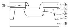
10: 반도체기판 12: 소자분리막10: semiconductor substrate 12: device isolation film
14: 산화막16: 제1 질화막14: oxide film 16: first nitride film
18: LDD영역20: 스페이서18: LDD region 20: spacer
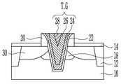
22: 게이트산화막24: 제1 도프드 폴리실리콘막22: gate oxide film 24: first doped polysilicon film
26: 제2 도프드 폴리실리콘막28: 제3 도프드 폴리실리콘막26: second doped polysilicon film 28: third doped polysilicon film
30: 소스/드레인영역T.G.P: 트렌치게이트전극패턴30: source / drain region T.G.P: trench gate electrode pattern
T.G: 트렌치게이트전극
TG: Trench Gate Electrode
본 발명은 반도체소자의 트랜지스터 제조방법에 관한 것으로, 더욱 상세하게는 트랜치 게이트전극을 구비한 반도체소자의 트랜지스터 제조방법에 관한 것이다.The present invention relates to a transistor manufacturing method of a semiconductor device, and more particularly to a transistor manufacturing method of a semiconductor device having a trench gate electrode.
최근 반도체소자가 고집적화됨에 따라 짧은 채널효과와 같은 문제점이 발생하여 충분한 채널길이를 확보할 수 있도록 하는 트랜지스터의 제조가 요구되고 있는 데, 이를 만족시키기 위해 트렌치를 이용하여 게이트전극을 형성하는 트렌치 게이트전극이 사용되고 있다.Recently, as semiconductor devices have been highly integrated, problems such as short channel effects have arisen, and thus, there is a demand for manufacturing a transistor that can secure sufficient channel length. To satisfy this, a trench gate electrode for forming a gate electrode using a trench is satisfied. Is being used.
상기와 같은 트렌치 게이트전극 형성시 언도프드 폴리실리콘막을 증착한 후 이온주입공정을 수행하여 도프드 폴리실리콘막의 트렌치 게이트전극을 형성하고, 상기 형성된 게이트전극 상부에 이온주입 방지용 마스크를 형성한 후 이온주입공정을 수행하여 소스/드레인영역을 형성한다.When forming the trench gate electrode as described above, an undoped polysilicon layer is deposited and an ion implantation process is performed to form a trench gate electrode of the doped polysilicon layer, and an ion implantation prevention mask is formed on the formed gate electrode, followed by ion implantation. The process is performed to form source / drain regions.
그러나 이 소스/드레인영역을 형성하기 위해 수행하는 이온주입공정시 주입된 이온이 이후 수행되는 열공정 등으로 인해 상기 트렌치 게이트전극을 형성하는 도프드 폴리실리콘막으로 확산되는 카운터 도핑(counter-doping)이 발생하여 효과적인 채널길이(effective channel length)가 줄어들게 되는 문제점이 있다.
However, in the ion implantation process performed to form the source / drain region, a counter-doping diffuses into the doped polysilicon layer forming the trench gate electrode due to a thermal process performed later. This occurs and there is a problem that the effective channel length (effective channel length) is reduced.
상술한 문제점을 해결하기 위한 본 발명의 목적은 소스/드레인영역과 트렌치 게이트전극들을 형성하는 이온들의 카운터 도핑발생을 억제하여 효과적인 채널길이를 확보할 수 있도록 하는 반도체소자의 트랜지스터 제조방법을 제공함에 있다.
SUMMARY OF THE INVENTION An object of the present invention is to provide a method of fabricating a transistor of a semiconductor device in which counter doping of ions forming source / drain regions and trench gate electrodes can be suppressed to ensure an effective channel length. .
상술한 목적을 달성하기 위한 본 발명의 사상은 반도체기판의 소정영역에 패터닝공정을 수행하여 트렌치게이트전극패턴을 형성하는 단계, 상기 형성된 트렌치게이트전극패턴에 언도프드 폴리실리콘막의 매립/이온주입공정으로 도프드 폴리실리콘막의 형성을 수행하는 단계 및 상기 언도프드 폴리실리콘막의 매립/이온주입공정으로 도프드 폴리실리콘막의 형성을 1회 이상 더 반복 수행하여 적어도 2층 이상 적층된 도프드 폴리실리콘막을 형성하여 트렌치게이트전극을 형성하는 단계를 포함한다.The idea of the present invention for achieving the above object is to form a trench gate electrode pattern by performing a patterning process on a predetermined region of a semiconductor substrate, the buried / ion implantation process of the undoped polysilicon film in the formed trench gate electrode pattern Performing the formation of the doped polysilicon film and the formation of the doped polysilicon film by repeating the formation of the doped polysilicon film one or more times in a buried / ion implantation process of the undoped polysilicon film to form at least two or more layers of the doped polysilicon film Forming a trench gate electrode.
상기 언도프드 폴리실리콘막은 500~ 550℃ 정도의 온도범위에서 0.1~ 3 torr 정도의 압력, SiH4 또는 Si2H6과 같은 Si 소스 가스와 PH3 가스분위기에서, 100~ 150Å 정도의 두께로 형성하는 것이 바람직하다.The undoped polysilicon film is formed at a thickness of about 100 to 150 kPa in a pressure of about 0.1 to 3 torr in a temperature range of about 500 to about 550 ° C., a Si source gas such as SiH4 or Si2 H6 , and a PH3 gas atmosphere. It is desirable to.
상기 이온주입공정은 10~ 25 Kev의 에너지대역에서 1E11~ 1E12ion/㎠의 도즈량으로 수행하는 것이 바람직하다.The ion implantation process is preferably carried out with a dose of 1E11 ~ 1E12ion / ㎠ in the energy band of 10 ~ 25 Kev.
이하, 첨부 도면을 참조하여 본 발명의 실시예를 상세히 설명한다. 그러나 본 발명의 실시예들은 여러 가지 다른 형태로 변형될 수 있지만 본 발명의 범위가 아래에서 상술하는 실시예들로 인해 한정되어지는 것으로 해석되어져서는 안 된다. 본 발명의 실시예들은 당업계에서 평균적인 지식을 가진 자에게 본 발명을 보다 완전하게 설명하기 위해 제공되어지는 것이다. 따라서, 도면에서의 막의 두께 등은 보다 명확한 설명을 강조하기 위해서 과장되어진 것이며, 도면상에서 동일한 부호로 표시된 요소는 동일한 요소를 의미한다. 또한 어떤 막이 다른 막 또는 반도체 기판의 '상'에 있다 또는 접촉하고 있다 라고 기재되는 경우에, 상기 어떤 막은 상기 다른 막 또는 반도체 기판에 직접 접촉하여 존재할 수 있고, 또는 그 사이에 제 3의 막이 개재되어질 수도 있다.Hereinafter, embodiments of the present invention will be described in detail with reference to the accompanying drawings. However, although the embodiments of the present invention may be modified in many different forms, the scope of the present invention should not be construed as being limited by the embodiments described below. Embodiments of the present invention are provided to more fully describe the present invention to those skilled in the art. Accordingly, the thickness of the film and the like in the drawings are exaggerated for clarity, and the elements denoted by the same reference numerals in the drawings mean the same elements. In addition, when a film is described as being on or in contact with another film or semiconductor substrate, the film may be in direct contact with the other film or semiconductor substrate, or a third film is interposed therebetween. It may be done.
도 1을 참조하면, 반도체기판(10)의 소정영역에 포토레지스트 패턴(미도시)을 형성한 후 이를 식각마스크로 식각공정을 수행하여 소자분리영역을 정의하는 트렌치(Trench; 미도시)를 형성한다. 상기 형성된 트렌치 내부에 갭필(gap fill)특성이 우수한 HDP(High Density plasma)산화막이 채워지도록 증착한 후 상기 반도체기판(10)이 노출될 때까지 화학적 기계적 연마(chemical mechanical polishing: CMP)공정 등의 평탄화공정을 수행하여 소자분리막(12)을 형성한다.Referring to FIG. 1, after forming a photoresist pattern (not shown) in a predetermined region of the
상기 결과물 상에 상기 소자분리막(12)의 형상을 보호하기 위해 제1 질화막(14) 및 트렌치 게이트전극용 산화막(16)을 순차적으로 형성한다.In order to protect the shape of the
상기 제1 질화막(14)은 반응기체로서 NH3와 SiH2Cl2가스를 이용하여 1~ 3torr 정도의 압력 및 650~ 800℃ 정도의 온도에서 LP- CVD법으로 50~ 65Å 정도의 두께로 형성할 수 있고, 상기 트렌치 게이트전극용 산화막(16)은 600~ 700℃ 정도의 온도, 1~ 3torr 정도의 압력 및 LP- CVD법으로 400~ 600Å 정도의 두께로 형성할 수 있다.The
상기 결과물의 소정영역에 포토레지스트패턴(PR)을 형성하고, 이를 식각마스 크로 하부의 산화막(16), 제1 질화막(14)을 순차적으로 식각하면, 반도체기판(10)의 소정영역이 노출되는 데, 이 영역은 이후 트렌치게이트전극이 형성되는 영역이다.When the photoresist pattern PR is formed in a predetermined region of the resultant, and the
상기 노출된 반도체기판(10)의 소정영역에 이온주입공정을 수행하여 LDD(lightly doped drain)영역(18)을 형성한다. 이때 상기 이온주입은 30~ 60 °틸티드하도록 진행되는 틸티드(tilted) 이온주입공정으로 수행하고, 1E14 내지 1E15ion/㎤ 정도의 도즈량, 20 내지 25KeV 정도의 이온주입에너지로 수행할 수 있다. 이어서 상기 형성된 포토레지스트 패턴(PR)을 제거하는 스트립공정을 수행한다.An ion implantation process is performed on a predetermined region of the exposed
도 2를 참조하면, 상기 결과물 전면에 제2 질화막을 형성한 후, 이를 식각하여 상기 제1 질화막(14) 및 산화막(16)의 측벽에 스페이서(20)를 형성한다.Referring to FIG. 2, after forming a second nitride film on the entire surface of the resultant, the
상기 제2 질화막은 반응기체로서 NH3와 SiH2Cl2가스를 이용하여 1~ 3torr 정도의 압력 및 650~ 800℃ 정도의 온도에서 LP- CVD법으로 50~ 65Å 정도의 두께로 형성할 수 있다.The second nitride film may be formed to a thickness of about 50 to 65 Pa by LP-CVD at a pressure of about 1 to 3 torr and a temperature of about 650 to 800 ° C. using NH3 and SiH2 Cl2 gas as a reactor. .
도 3을 참조하면, 상기 제1 질화막(14), 산화막(16) 및 스페이서(20)를 식각마스크로 상기 반도체기판(10)에 식각공정을 수행하여 트렌치게이트전극패턴(T.G.P)을 형성한다. 상기 트렌치게이트전극패턴(T.G.P) 상부에 게이트 산화막(22)을 형성하는 데, 이는 750~ 850℃ 정도의 온도에서 건식 또는 습식산화공정을 진행한 후 900~ 910℃ 정도의 온도에서 N2가스를 이용하여 20~ 30분 간 어닐링공정을 수행하여 50~ 70Å 정도의 두께로 형성할 수 있다.Referring to FIG. 3, a trench gate electrode pattern TGP is formed by performing an etching process on the
이어서, 상기 게이트산화막(22)이 형성된 트렌치게이트전극패턴(T.G.P)을 매립하기 위해 도프드 폴리실리콘막을 형성하는 데, 이는 3층으로 이루어진 도프드 폴리실리콘막을 형성한다. 즉, 제1 언도프드 폴리실리콘막을 형성한 후 이온주입공정을 수행하여 제1 도프드 폴리실리콘막(24)을 형성하고, 상기 제1 도프드 폴리실리콘막(24)상부에 제2 언도프드 폴리실리콘막을 형성한 후 이온주입공정을 수행하여 제2 도프드 폴리실리콘막(26)을 형성하고, 제2 도포드 폴리실리콘막(26) 상부에 제3 언도프프 폴리실리콘막을 형성한 후 이온주입공정을 수행하여 제3 도프드 폴리실리콘막(28)을 형성함으로써, 트렌치게이트전극패턴(T.G.P)을 매립한다.Subsequently, a doped polysilicon film is formed to fill the trench gate electrode pattern T.G.P in which the
상기 제1, 제2 및 제3 언도프드 폴리실리콘막(24, 26, 28)은 500~ 550℃ 정도의 온도범위에서 0.1~ 3 torr 정도의 압력, SiH4 또는 Si2H6과 같은 Si 소스 가스와 PH3 가스분위기에서 언도프드 폴리실리콘(undoped Poly Silcon)막을 100~ 150Å 정도의 두께로 각각 형성할 수 있다.The first, second and third
상기 이온주입공정들은 10~ 25 Kev의 에너지대역에서 1E11~ 1E12ion/㎠의 도즈량으로 각각 수행한다.The ion implantation processes are performed with doses of 1E11-1E12ion / cm 2 in an energy band of 10-25 Kev.
상기와 같은 제1 언도프드 폴리실리콘막의 증착 후 이온주입공정으로 제1 도프드 폴리실리콘막의 형성을 진행하는 것을 하나의 과정으로 보았을 때, 이 과정을 3회 반복 수행하여 3층의 도프드 폴리실리콘막으로 형성된 트렌치 게이트전극을 형성하게 된다. 상기 제1 과정의 수행시 제1 도프드 폴리실리콘막의 도핑영역은 종래 기술보다 좁은 영역이므로 종래 기술과 동일한 이온주입량에 대해 더 좁은 영역에 이온주입공정을 수행하기 때문에, 이온 주입된 상기 영역의 이온밀도는 높아지게 되고, 이후 수행되는 공정들에 의해 상기 높아진 이온밀도를 가진 영역들 간의 카운터 도핑이온의 양은 현저히 줄어들게 된다. 따라서 카운터 도핑이 감소된 각 영역들로 인해 효과적인 채널길이를 확보할 수 있게 된다.When the formation of the first doped polysilicon film is performed by the ion implantation process after the deposition of the first undoped polysilicon film as described above as a single process, the process is repeated three times to obtain three layers of doped polysilicon. A trench gate electrode formed of a film is formed. Since the doping region of the first doped polysilicon film is narrower than that of the prior art, the ion implantation process is performed in a narrower region for the same amount of ion implantation as in the prior art. The density is increased, and the processes performed thereafter significantly reduce the amount of counter doping ions between the regions with the higher ion density. Therefore, the effective channel length can be ensured due to the areas where the counter doping is reduced.
도 4를 참조하면, 상기 형성된 제1, 제2 제3 도프드 폴리실리콘막(24, 26, 28)을 에치백하여 상기 기판(10)에 형성된 트렌치를 매립하는 트렌치게이트전극(T.G)을 형성한다. 이어서 상기 트렌치게이트전극용 산화막(16)을 제거하는 습식식각공정을 수행한다. 이때 반도체기판(10) 표면에 형성된 제1 질화막(14)이 식각정지막으로 작용하여 반도체기판(10) 및 소자분리막(12)의 손상을 방지할 수 있도록 한다.Referring to FIG. 4, a trench gate electrode TG is formed to etch back the formed first and second third doped
도 5를 참조하면, 상기 형성된 트렌치게이트전극(T.G)을 이온주입용 마스크로 하여 이온주입공정을 수행하여 소스/드레인영역(30)을 형성하여 트렌치게이트전극을 구비한 트랜지스터의 형성을 완료한다.Referring to FIG. 5, an ion implantation process is performed using the formed trench gate electrode T.G as an ion implantation mask to form a source /
본 발명에 의하면 트렌치 게이트전극 형성시 언도프드 폴리실리콘막의 증착/이온주입으로 도프드 폴리실리콘막의 형성과 같은 과정을 3회 수행하여 트렌치게이트전극을 형성함으로써, 트렌치 게이트전극과 소스/드레인영역간의 카운터 도핑을 줄일 수 있게 되어 효과적인 채널길이를 확보할 수 있도록 한다.According to the present invention, a trench gate electrode is formed by performing the same process three times as the formation of the doped polysilicon film by deposition / ion implantation of an undoped polysilicon film during the formation of the trench gate electrode, thereby forming a counter between the trench gate electrode and the source / drain region. Doping can be reduced to ensure an effective channel length.
본 발명의 바람직한 일 실시예에서는 언도프드 폴리실리콘막의 증착/이온주입으로 도프드 폴리실리콘막의 형성과 같은 과정을 3회만 수행하는 것을 제시하고 있지만, 카운터 도핑발생을 억제하기 위해서는 상기 과정의 횟수는 한정하지 않고 반복 사용할 수 있다.
In a preferred embodiment of the present invention, it is proposed that the process of forming the doped polysilicon film is performed only three times by deposition / ion implantation of the undoped polysilicon film, but the number of times of the process is limited to suppress the occurrence of counter doping. Can be used repeatedly without.
이상에서 살펴본 바와 같이 본 발명에 의하면 트렌치 게이트전극 형성시 언도프드 폴리실리콘막의 증착/이온주입을 통한 도프드 폴리실리콘막의 형성과 같은 과정을 3회 이상 수행하여 트렌치 게이트전극을 형성함으로써, 트렌치 게이트전극과 소스/드레인영역간의 카운터 도핑을 줄일 수 있게 되어 효과적인 채널길이를 확보할 수 있도록 하는 효과가 있다.As described above, according to the present invention, the trench gate electrode is formed by performing the same process as the formation of the doped polysilicon film through the deposition / ion implantation of the undoped polysilicon film at least three times to form the trench gate electrode. It is possible to reduce the counter doping between the and source / drain regions, thereby ensuring an effective channel length.
본 발명은 구체적인 실시 예에 대해서만 상세히 설명하였지만 본 발명의 기술적 사상의 범위 내에서 변형이나 변경할 수 있음은 본 발명이 속하는 분야의 당업자에게는 명백한 것이며, 그러한 변형이나 변경은 본 발명의 특허청구범위에 속한다 할 것이다.Although the present invention has been described in detail only with respect to specific embodiments, it is apparent to those skilled in the art that modifications or changes can be made within the scope of the technical idea of the present invention, and such modifications or changes belong to the claims of the present invention. something to do.
Claims (3)
Translated fromKoreanPriority Applications (1)
| Application Number | Priority Date | Filing Date | Title |
|---|---|---|---|
| KR1020030047115AKR101017051B1 (en) | 2003-07-11 | 2003-07-11 | Transistor manufacturing method of semiconductor device |
Applications Claiming Priority (1)
| Application Number | Priority Date | Filing Date | Title |
|---|---|---|---|
| KR1020030047115AKR101017051B1 (en) | 2003-07-11 | 2003-07-11 | Transistor manufacturing method of semiconductor device |
Publications (2)
| Publication Number | Publication Date |
|---|---|
| KR20050007637A KR20050007637A (en) | 2005-01-21 |
| KR101017051B1true KR101017051B1 (en) | 2011-02-23 |
Family
ID=37220985
Family Applications (1)
| Application Number | Title | Priority Date | Filing Date |
|---|---|---|---|
| KR1020030047115AExpired - Fee RelatedKR101017051B1 (en) | 2003-07-11 | 2003-07-11 | Transistor manufacturing method of semiconductor device |
Country Status (1)
| Country | Link |
|---|---|
| KR (1) | KR101017051B1 (en) |
Cited By (2)
| Publication number | Priority date | Publication date | Assignee | Title |
|---|---|---|---|---|
| US8993391B2 (en) | 2012-12-27 | 2015-03-31 | SK Hynix Inc. | Semiconductor device with recess gate and method for fabricating the same |
| US9960350B2 (en) | 2016-06-03 | 2018-05-01 | SK Hynix Inc. | Method of fabricating switching element and method of manufacturing resistive memory device |
Families Citing this family (6)
| Publication number | Priority date | Publication date | Assignee | Title |
|---|---|---|---|---|
| KR100685678B1 (en)* | 2005-03-29 | 2007-02-26 | 주식회사 하이닉스반도체 | Recess channel array transistor and manufacturing method thereof |
| KR100798790B1 (en)* | 2005-08-29 | 2008-01-29 | 주식회사 하이닉스반도체 | Semiconductor device manufacturing method |
| KR100711520B1 (en) | 2005-09-12 | 2007-04-27 | 삼성전자주식회사 | A structure for a recessed gate electrode, a method of forming the same, and a method of manufacturing the semiconductor device comprising the recessed gate electrode. |
| KR100703027B1 (en) | 2005-09-26 | 2007-04-06 | 삼성전자주식회사 | How to form recess gate |
| KR100689840B1 (en) | 2005-10-04 | 2007-03-08 | 삼성전자주식회사 | Semiconductor device having recessed gate electrode and method of manufacturing same |
| KR101035612B1 (en)* | 2008-09-04 | 2011-05-19 | 주식회사 동부하이텍 | Semiconductor element and manufacturing method thereof |
Citations (4)
| Publication number | Priority date | Publication date | Assignee | Title |
|---|---|---|---|---|
| JPH02285667A (en)* | 1989-04-27 | 1990-11-22 | Toshiba Corp | Manufacturing method of semiconductor device |
| US5429970A (en) | 1994-07-18 | 1995-07-04 | United Microelectronics Corporation | Method of making flash EEPROM memory cell |
| US6147377A (en) | 1998-03-30 | 2000-11-14 | Advanced Micro Devices, Inc. | Fully recessed semiconductor device |
| US20050122848A1 (en)* | 2003-12-04 | 2005-06-09 | Montres Breguet S.A. | Detent escapement for a timepiece |
- 2003
- 2003-07-11KRKR1020030047115Apatent/KR101017051B1/ennot_activeExpired - Fee Related
Patent Citations (4)
| Publication number | Priority date | Publication date | Assignee | Title |
|---|---|---|---|---|
| JPH02285667A (en)* | 1989-04-27 | 1990-11-22 | Toshiba Corp | Manufacturing method of semiconductor device |
| US5429970A (en) | 1994-07-18 | 1995-07-04 | United Microelectronics Corporation | Method of making flash EEPROM memory cell |
| US6147377A (en) | 1998-03-30 | 2000-11-14 | Advanced Micro Devices, Inc. | Fully recessed semiconductor device |
| US20050122848A1 (en)* | 2003-12-04 | 2005-06-09 | Montres Breguet S.A. | Detent escapement for a timepiece |
Cited By (2)
| Publication number | Priority date | Publication date | Assignee | Title |
|---|---|---|---|---|
| US8993391B2 (en) | 2012-12-27 | 2015-03-31 | SK Hynix Inc. | Semiconductor device with recess gate and method for fabricating the same |
| US9960350B2 (en) | 2016-06-03 | 2018-05-01 | SK Hynix Inc. | Method of fabricating switching element and method of manufacturing resistive memory device |
Also Published As
| Publication number | Publication date |
|---|---|
| KR20050007637A (en) | 2005-01-21 |
Similar Documents
| Publication | Publication Date | Title |
|---|---|---|
| KR100338778B1 (en) | Method for fabricating MOS transistor using selective silicide process | |
| KR101017051B1 (en) | Transistor manufacturing method of semiconductor device | |
| KR100683401B1 (en) | Semiconductor Device Using Epilayer and Manufacturing Method Thereof | |
| KR100554836B1 (en) | Manufacturing Method of Flash Memory Device | |
| KR20000013397A (en) | Manufacturing method of trench isolation | |
| KR100951740B1 (en) | Manufacturing Method of Semiconductor Device | |
| US20080067616A1 (en) | Semiconductor device | |
| KR100542394B1 (en) | Gate electrode formation method of flash memory device | |
| KR100275732B1 (en) | Method for forming a trench type device isolation film uisng an anneling | |
| KR100530420B1 (en) | Method of manufacturing in flash memory device | |
| KR20100088350A (en) | Method of fabricating a semiconductor device | |
| KR101072996B1 (en) | Method of manufacturing in semiconductor device | |
| KR101016336B1 (en) | Manufacturing Method of Flash Memory Device | |
| KR100702324B1 (en) | Semiconductor device and manufacturing method thereof | |
| KR100344765B1 (en) | Method for isolating semiconductor devices | |
| KR101253740B1 (en) | Method for manufacturing a semiconductor device | |
| KR100511679B1 (en) | Method of forming device's isolation layer in semiconductor device | |
| KR100870357B1 (en) | Manufacturing Method of Semiconductor Device | |
| KR100832706B1 (en) | Semiconductor device and manufacturing method thereof | |
| KR20050009497A (en) | Method of manufacturing a transistor in a semiconductor device | |
| KR100672757B1 (en) | Method of manufacturing semiconductor device for forming shallow junction | |
| KR100467642B1 (en) | Fabricating method of semiconductor device | |
| KR100469333B1 (en) | Method of manufacturing a semiconductor device | |
| KR20060074174A (en) | Gate electrode pattern formation method of flash memory device | |
| KR20020041191A (en) | Device and method for semiconductor device |
Legal Events
| Date | Code | Title | Description |
|---|---|---|---|
| PA0109 | Patent application | St.27 status event code:A-0-1-A10-A12-nap-PA0109 | |
| N231 | Notification of change of applicant | ||
| PN2301 | Change of applicant | St.27 status event code:A-3-3-R10-R13-asn-PN2301 St.27 status event code:A-3-3-R10-R11-asn-PN2301 | |
| R17-X000 | Change to representative recorded | St.27 status event code:A-3-3-R10-R17-oth-X000 | |
| PG1501 | Laying open of application | St.27 status event code:A-1-1-Q10-Q12-nap-PG1501 | |
| PN2301 | Change of applicant | St.27 status event code:A-3-3-R10-R13-asn-PN2301 St.27 status event code:A-3-3-R10-R11-asn-PN2301 | |
| A201 | Request for examination | ||
| PA0201 | Request for examination | St.27 status event code:A-1-2-D10-D11-exm-PA0201 | |
| R17-X000 | Change to representative recorded | St.27 status event code:A-3-3-R10-R17-oth-X000 | |
| D13-X000 | Search requested | St.27 status event code:A-1-2-D10-D13-srh-X000 | |
| R17-X000 | Change to representative recorded | St.27 status event code:A-3-3-R10-R17-oth-X000 | |
| D14-X000 | Search report completed | St.27 status event code:A-1-2-D10-D14-srh-X000 | |
| E902 | Notification of reason for refusal | ||
| PE0902 | Notice of grounds for rejection | St.27 status event code:A-1-2-D10-D21-exm-PE0902 | |
| P11-X000 | Amendment of application requested | St.27 status event code:A-2-2-P10-P11-nap-X000 | |
| P13-X000 | Application amended | St.27 status event code:A-2-2-P10-P13-nap-X000 | |
| E701 | Decision to grant or registration of patent right | ||
| PE0701 | Decision of registration | St.27 status event code:A-1-2-D10-D22-exm-PE0701 | |
| GRNT | Written decision to grant | ||
| PR0701 | Registration of establishment | St.27 status event code:A-2-4-F10-F11-exm-PR0701 | |
| PR1002 | Payment of registration fee | St.27 status event code:A-2-2-U10-U11-oth-PR1002 Fee payment year number:1 | |
| PG1601 | Publication of registration | St.27 status event code:A-4-4-Q10-Q13-nap-PG1601 | |
| FPAY | Annual fee payment | Payment date:20140116 Year of fee payment:4 | |
| PR1001 | Payment of annual fee | St.27 status event code:A-4-4-U10-U11-oth-PR1001 Fee payment year number:4 | |
| FPAY | Annual fee payment | Payment date:20150116 Year of fee payment:5 | |
| PR1001 | Payment of annual fee | St.27 status event code:A-4-4-U10-U11-oth-PR1001 Fee payment year number:5 | |
| FPAY | Annual fee payment | Payment date:20160119 Year of fee payment:6 | |
| PR1001 | Payment of annual fee | St.27 status event code:A-4-4-U10-U11-oth-PR1001 Fee payment year number:6 | |
| FPAY | Annual fee payment | Payment date:20170117 Year of fee payment:7 | |
| PR1001 | Payment of annual fee | St.27 status event code:A-4-4-U10-U11-oth-PR1001 Fee payment year number:7 | |
| FPAY | Annual fee payment | Payment date:20180116 Year of fee payment:8 | |
| PR1001 | Payment of annual fee | St.27 status event code:A-4-4-U10-U11-oth-PR1001 Fee payment year number:8 | |
| P22-X000 | Classification modified | St.27 status event code:A-4-4-P10-P22-nap-X000 | |
| FPAY | Annual fee payment | Payment date:20190117 Year of fee payment:9 | |
| PR1001 | Payment of annual fee | St.27 status event code:A-4-4-U10-U11-oth-PR1001 Fee payment year number:9 | |
| FPAY | Annual fee payment | Payment date:20200116 Year of fee payment:10 | |
| PR1001 | Payment of annual fee | St.27 status event code:A-4-4-U10-U11-oth-PR1001 Fee payment year number:10 | |
| PN2301 | Change of applicant | St.27 status event code:A-5-5-R10-R11-asn-PN2301 | |
| PN2301 | Change of applicant | St.27 status event code:A-5-5-R10-R14-asn-PN2301 | |
| R18-X000 | Changes to party contact information recorded | St.27 status event code:A-5-5-R10-R18-oth-X000 | |
| PR1001 | Payment of annual fee | St.27 status event code:A-4-4-U10-U11-oth-PR1001 Fee payment year number:11 | |
| PC1903 | Unpaid annual fee | St.27 status event code:A-4-4-U10-U13-oth-PC1903 Not in force date:20220217 Payment event data comment text:Termination Category : DEFAULT_OF_REGISTRATION_FEE | |
| PN2301 | Change of applicant | St.27 status event code:A-5-5-R10-R13-asn-PN2301 St.27 status event code:A-5-5-R10-R11-asn-PN2301 | |
| PC1903 | Unpaid annual fee | St.27 status event code:N-4-6-H10-H13-oth-PC1903 Ip right cessation event data comment text:Termination Category : DEFAULT_OF_REGISTRATION_FEE Not in force date:20220217 | |
| P22-X000 | Classification modified | St.27 status event code:A-4-4-P10-P22-nap-X000 |