KR101014778B1 - Chip antenna and semiconductor package, and ultra-wideband communication system including the same - Google Patents
Chip antenna and semiconductor package, and ultra-wideband communication system including the sameDownload PDFInfo
- Publication number
- KR101014778B1 KR101014778B1KR1020080018231AKR20080018231AKR101014778B1KR 101014778 B1KR101014778 B1KR 101014778B1KR 1020080018231 AKR1020080018231 AKR 1020080018231AKR 20080018231 AKR20080018231 AKR 20080018231AKR 101014778 B1KR101014778 B1KR 101014778B1
- Authority
- KR
- South Korea
- Prior art keywords
- pad
- chip
- antenna
- lead frame
- semiconductor chip
- Prior art date
- Legal status (The legal status is an assumption and is not a legal conclusion. Google has not performed a legal analysis and makes no representation as to the accuracy of the status listed.)
- Expired - Fee Related
Links
Images

Classifications
- H—ELECTRICITY
- H01—ELECTRIC ELEMENTS
- H01L—SEMICONDUCTOR DEVICES NOT COVERED BY CLASS H10
- H01L24/00—Arrangements for connecting or disconnecting semiconductor or solid-state bodies; Methods or apparatus related thereto
- H01L24/01—Means for bonding being attached to, or being formed on, the surface to be connected, e.g. chip-to-package, die-attach, "first-level" interconnects; Manufacturing methods related thereto
- H01L24/42—Wire connectors; Manufacturing methods related thereto
- H01L24/47—Structure, shape, material or disposition of the wire connectors after the connecting process
- H01L24/49—Structure, shape, material or disposition of the wire connectors after the connecting process of a plurality of wire connectors
- H—ELECTRICITY
- H01—ELECTRIC ELEMENTS
- H01L—SEMICONDUCTOR DEVICES NOT COVERED BY CLASS H10
- H01L2224/00—Indexing scheme for arrangements for connecting or disconnecting semiconductor or solid-state bodies and methods related thereto as covered by H01L24/00
- H01L2224/01—Means for bonding being attached to, or being formed on, the surface to be connected, e.g. chip-to-package, die-attach, "first-level" interconnects; Manufacturing methods related thereto
- H01L2224/02—Bonding areas; Manufacturing methods related thereto
- H01L2224/04—Structure, shape, material or disposition of the bonding areas prior to the connecting process
- H01L2224/05—Structure, shape, material or disposition of the bonding areas prior to the connecting process of an individual bonding area
- H01L2224/0554—External layer
- H01L2224/0555—Shape
- H01L2224/05552—Shape in top view
- H01L2224/05554—Shape in top view being square
- H—ELECTRICITY
- H01—ELECTRIC ELEMENTS
- H01L—SEMICONDUCTOR DEVICES NOT COVERED BY CLASS H10
- H01L2224/00—Indexing scheme for arrangements for connecting or disconnecting semiconductor or solid-state bodies and methods related thereto as covered by H01L24/00
- H01L2224/01—Means for bonding being attached to, or being formed on, the surface to be connected, e.g. chip-to-package, die-attach, "first-level" interconnects; Manufacturing methods related thereto
- H01L2224/42—Wire connectors; Manufacturing methods related thereto
- H01L2224/44—Structure, shape, material or disposition of the wire connectors prior to the connecting process
- H01L2224/45—Structure, shape, material or disposition of the wire connectors prior to the connecting process of an individual wire connector
- H01L2224/45001—Core members of the connector
- H01L2224/45099—Material
- H01L2224/451—Material with a principal constituent of the material being a metal or a metalloid, e.g. boron (B), silicon (Si), germanium (Ge), arsenic (As), antimony (Sb), tellurium (Te) and polonium (Po), and alloys thereof
- H01L2224/45138—Material with a principal constituent of the material being a metal or a metalloid, e.g. boron (B), silicon (Si), germanium (Ge), arsenic (As), antimony (Sb), tellurium (Te) and polonium (Po), and alloys thereof the principal constituent melting at a temperature of greater than or equal to 950°C and less than 1550°C
- H01L2224/45139—Silver (Ag) as principal constituent
- H—ELECTRICITY
- H01—ELECTRIC ELEMENTS
- H01L—SEMICONDUCTOR DEVICES NOT COVERED BY CLASS H10
- H01L2224/00—Indexing scheme for arrangements for connecting or disconnecting semiconductor or solid-state bodies and methods related thereto as covered by H01L24/00
- H01L2224/01—Means for bonding being attached to, or being formed on, the surface to be connected, e.g. chip-to-package, die-attach, "first-level" interconnects; Manufacturing methods related thereto
- H01L2224/42—Wire connectors; Manufacturing methods related thereto
- H01L2224/47—Structure, shape, material or disposition of the wire connectors after the connecting process
- H01L2224/48—Structure, shape, material or disposition of the wire connectors after the connecting process of an individual wire connector
- H01L2224/4805—Shape
- H01L2224/4809—Loop shape
- H01L2224/48091—Arched
- H—ELECTRICITY
- H01—ELECTRIC ELEMENTS
- H01L—SEMICONDUCTOR DEVICES NOT COVERED BY CLASS H10
- H01L2224/00—Indexing scheme for arrangements for connecting or disconnecting semiconductor or solid-state bodies and methods related thereto as covered by H01L24/00
- H01L2224/01—Means for bonding being attached to, or being formed on, the surface to be connected, e.g. chip-to-package, die-attach, "first-level" interconnects; Manufacturing methods related thereto
- H01L2224/42—Wire connectors; Manufacturing methods related thereto
- H01L2224/47—Structure, shape, material or disposition of the wire connectors after the connecting process
- H01L2224/49—Structure, shape, material or disposition of the wire connectors after the connecting process of a plurality of wire connectors
- H01L2224/491—Disposition
- H01L2224/4911—Disposition the connectors being bonded to at least one common bonding area, e.g. daisy chain
- H01L2224/49113—Disposition the connectors being bonded to at least one common bonding area, e.g. daisy chain the connectors connecting different bonding areas on the semiconductor or solid-state body to a common bonding area outside the body, e.g. converging wires
- H—ELECTRICITY
- H01—ELECTRIC ELEMENTS
- H01L—SEMICONDUCTOR DEVICES NOT COVERED BY CLASS H10
- H01L2924/00—Indexing scheme for arrangements or methods for connecting or disconnecting semiconductor or solid-state bodies as covered by H01L24/00
- H01L2924/0001—Technical content checked by a classifier
- H01L2924/00014—Technical content checked by a classifier the subject-matter covered by the group, the symbol of which is combined with the symbol of this group, being disclosed without further technical details
- H—ELECTRICITY
- H01—ELECTRIC ELEMENTS
- H01L—SEMICONDUCTOR DEVICES NOT COVERED BY CLASS H10
- H01L2924/00—Indexing scheme for arrangements or methods for connecting or disconnecting semiconductor or solid-state bodies as covered by H01L24/00
- H01L2924/01—Chemical elements
- H01L2924/01014—Silicon [Si]
- H—ELECTRICITY
- H01—ELECTRIC ELEMENTS
- H01L—SEMICONDUCTOR DEVICES NOT COVERED BY CLASS H10
- H01L2924/00—Indexing scheme for arrangements or methods for connecting or disconnecting semiconductor or solid-state bodies as covered by H01L24/00
- H01L2924/01—Chemical elements
- H01L2924/01033—Arsenic [As]
- H—ELECTRICITY
- H01—ELECTRIC ELEMENTS
- H01L—SEMICONDUCTOR DEVICES NOT COVERED BY CLASS H10
- H01L2924/00—Indexing scheme for arrangements or methods for connecting or disconnecting semiconductor or solid-state bodies as covered by H01L24/00
- H01L2924/01—Chemical elements
- H01L2924/01047—Silver [Ag]
- H—ELECTRICITY
- H01—ELECTRIC ELEMENTS
- H01L—SEMICONDUCTOR DEVICES NOT COVERED BY CLASS H10
- H01L2924/00—Indexing scheme for arrangements or methods for connecting or disconnecting semiconductor or solid-state bodies as covered by H01L24/00
- H01L2924/01—Chemical elements
- H01L2924/01079—Gold [Au]
- H—ELECTRICITY
- H01—ELECTRIC ELEMENTS
- H01L—SEMICONDUCTOR DEVICES NOT COVERED BY CLASS H10
- H01L2924/00—Indexing scheme for arrangements or methods for connecting or disconnecting semiconductor or solid-state bodies as covered by H01L24/00
- H01L2924/01—Chemical elements
- H01L2924/01082—Lead [Pb]
- H—ELECTRICITY
- H01—ELECTRIC ELEMENTS
- H01L—SEMICONDUCTOR DEVICES NOT COVERED BY CLASS H10
- H01L2924/00—Indexing scheme for arrangements or methods for connecting or disconnecting semiconductor or solid-state bodies as covered by H01L24/00
- H01L2924/013—Alloys
- H01L2924/014—Solder alloys
- H—ELECTRICITY
- H01—ELECTRIC ELEMENTS
- H01L—SEMICONDUCTOR DEVICES NOT COVERED BY CLASS H10
- H01L2924/00—Indexing scheme for arrangements or methods for connecting or disconnecting semiconductor or solid-state bodies as covered by H01L24/00
- H01L2924/10—Details of semiconductor or other solid state devices to be connected
- H01L2924/11—Device type
- H01L2924/13—Discrete devices, e.g. 3 terminal devices
- H01L2924/1304—Transistor
- H01L2924/1306—Field-effect transistor [FET]
- H—ELECTRICITY
- H01—ELECTRIC ELEMENTS
- H01L—SEMICONDUCTOR DEVICES NOT COVERED BY CLASS H10
- H01L2924/00—Indexing scheme for arrangements or methods for connecting or disconnecting semiconductor or solid-state bodies as covered by H01L24/00
- H01L2924/10—Details of semiconductor or other solid state devices to be connected
- H01L2924/11—Device type
- H01L2924/14—Integrated circuits
Landscapes
- Engineering & Computer Science (AREA)
- Computer Hardware Design (AREA)
- Microelectronics & Electronic Packaging (AREA)
- Power Engineering (AREA)
- Variable-Direction Aerials And Aerial Arrays (AREA)
- Semiconductor Integrated Circuits (AREA)
Abstract
Translated fromKoreanDescription
Translated fromKorean본 발명은 칩 안테나와 반도체 패키지 및 이를 포함하는 초광대역 통신 시스템에 관한 것이다. 보다 상세하게는 반도체 칩 상의 패드와 기판의 리드 프레임을 와이어로 연결하여 충분한 길이의 초경량 초소형 칩 안테나를 구현함으로써 UWB 통신 시스템의 동작 주파수 대역 환경도 충분히 커버함과 아울러, 스위치를 이용하여 여러 개의 서브 안테나를 구현함으로써 안테나 길이를 조절할 수 있도록 하여 필요에 따라 주파수 대역을 프로그래머블(programmable)하게 사용할 수 있을 뿐만 아니라, 외부 핀의 확보를 위해 비아 홀을 형성함으로써 칩 안테나를 위한 패드의 개수를 충분히 확보함과 더불어 칩 외부와의 전기적 연결을 위한 외부 핀의 개수도 충분히 확보할 수 있는 칩 안테나와 반도체 패키지 및 이를 포함하는 초광대역 통신 시스템에 관한 것이다.The present invention relates to a chip antenna, a semiconductor package, and an ultra-wideband communication system including the same. More specifically, by connecting a pad on a semiconductor chip and a lead frame of a substrate with wires to realize an ultra-light micro chip antenna having a sufficient length, it sufficiently covers the operating frequency band environment of the UWB communication system and uses a plurality of subs by using a switch. By implementing the antenna, the length of the antenna can be adjusted so that the frequency band can be programmed as needed, and via holes are formed to secure external pins, thereby sufficiently securing the number of pads for the chip antenna. In addition, the present invention relates to a chip antenna, a semiconductor package, and an ultra-wideband communication system including the same, which can sufficiently secure the number of external pins for electrical connection to the outside of the chip.
초광대역(UWB, Ultra Wide Band) 통신은 넓은 주파수 대역을 이용하여 대용량의 데이터를 고속으로 송수신할 수 있다. 이러한 특성 때문에 UWB 통신은 차세대 무선 데이터 통신으로 주목받고 있으며, 특히 10m 정도의 근거리에 있는 PC, TV, PDA, DVD, 디지털 카메라, 프린터 등을 연결하는 개인 통신망이나, 홈 네트워크, 위치 추적 시스템, 자동차의 충돌방지 시스템, 의료 기기 등에 폭넓게 사용될 것으로 예상된다.Ultra Wide Band (UWB) communication can transmit and receive large amounts of data at high speed using a wide frequency band. Because of these characteristics, UWB communication is attracting attention as the next generation wireless data communication, especially personal network connecting PCs, TVs, PDAs, DVDs, digital cameras, printers, etc., which are about 10m away, home networks, location tracking systems, and automobiles. It is expected to be widely used in anti-collision systems, medical devices, and the like.
이와 같이 UWB 통신 시스템은 개인 무선 휴대장비에 장착되는 관계로, 소형화가 필수적이다. UWB 통신 시스템의 소형화에 있어 문제되는 것이 안테나이다. 안테나는 일반적으로 파장의 1/4 정도의 길이를 필요로 하므로, 안테나의 소형화에는 물리적 한계가 존재하게 된다.As such, since UWB communication systems are installed in personal wireless portable devices, miniaturization is essential. The problem in miniaturizing a UWB communication system is an antenna. Since the antenna generally needs about one quarter of the wavelength, there are physical limitations to the miniaturization of the antenna.
안테나를 소형화하기 위해 제안된 종래 기술로는 곡류(meander) 형태의 안테나가 있다. 곡류 형태의 안테나는 일정한 면적 내에서 보다 긴 길이를 갖는 안테나를 구현하기 위한 것으로, 여러 층이 적층된 반도체 패키지의 각 층에 곡류 형태의 안테나를 구비하는 집적형 멘더 안테나가 제안되기도 하였다. 그러나, 곡류 형태의 안테나라 할지라도 반도체 패키지의 물리적 크기는 제한될 수밖에 없으므로 대략 24GHz 대역에서 동작해야 한다. 따라서, 이러한 안테나는 3~10GHz의 동작 범위를 갖는 UWB 통신 시스템에 적용되기 어려운 문제점이 있다.A conventional technique proposed for miniaturizing the antenna is a meander shaped antenna. The grain-type antenna is to implement an antenna having a longer length within a predetermined area, and an integrated mender antenna having a grain-shaped antenna on each layer of a semiconductor package in which several layers are stacked has been proposed. However, even in the form of a grain-shaped antenna, the physical size of the semiconductor package is inevitably limited, so it must operate in approximately 24 GHz band. Therefore, such an antenna is difficult to be applied to a UWB communication system having an operating range of 3 ~ 10GHz.
다른 종래 기술로는 패치형 집적 안테나가 제안된 바 있다. 패치형 집적 안테나는 실리콘 기판 상에 패드 층(pad layer)의 패치(patch)를 형성한 것이다. 그러나, 이러한 패치형 집적 안테나의 경우에도 물리적 크기의 한계로 사용 주파수가 대략 410GHz에 이르므로, 3~10GHz의 동작 범위를 갖는 UWB 통신 시스템에 적용되기 어려운 문제점이 있다.Another prior art has been proposed a patch type integrated antenna. A patch type integrated antenna is a patch of a pad layer on a silicon substrate. However, such a patch type integrated antenna also has a problem in that it is difficult to be applied to a UWB communication system having an operating range of 3 to 10 GHz since the use frequency reaches approximately 410 GHz due to the limitation of physical size.
본 발명은 상기와 같은 문제점을 해결하기 위해 안출된 것으로, 특히 충분한 길이의 초경량 초소형 칩 안테나를 구현함으로써 UWB 통신 시스템의 동작 주파수 대역 환경도 충분히 커버함과 아울러, 안테나 길이를 조절할 수 있도록 하여 필요에 따라 주파수 대역을 프로그래머블(programmable)하게 사용할 수 있을 뿐만 아니라, 칩 안테나를 위한 패드의 개수를 충분히 확보함과 더불어 칩 외부와의 전기적 연결을 위한 외부 핀의 개수도 충분히 확보할 수 있는 칩 안테나와 반도체 패키지 및 이를 포함하는 초광대역 통신 시스템을 제공하는 데 그 목적이 있다.SUMMARY OF THE INVENTION The present invention has been made to solve the above problems, and in particular, by implementing an ultra-lightweight microchip antenna of sufficient length, it is possible to sufficiently cover the operating frequency band environment of the UWB communication system and to adjust the antenna length. According to the present invention, chip antennas and semiconductors can be used not only programmable to the frequency band, but also to secure a sufficient number of pads for the chip antenna and to secure enough external pins for electrical connection to the outside of the chip. An object of the present invention is to provide a package and an ultra wideband communication system including the same.
상기 목적을 달성하기 위해 안출된 본 발명에 따른 칩 안테나는 반도체 칩 상의 패드(pad); 상기 반도체 칩이 장착되는 기판(substrate)의 리드 프레임(lead frame); 및 상기 패드와 상기 리드 프레임을 전기적으로 연결하는 와이어(wire)를 포함하는 것을 특징으로 한다.In order to achieve the above object, a chip antenna according to the present invention includes a pad on a semiconductor chip; A lead frame of a substrate on which the semiconductor chip is mounted; And a wire for electrically connecting the pad and the lead frame.
또한, 상기 패드 중 적어도 어느 하나는 상기 반도체 칩의 송신부 또는 수신부와 전기적으로 연결될 수 있다.In addition, at least one of the pads may be electrically connected to a transmitter or receiver of the semiconductor chip.
또한, 상기 패드는 제1 패드 내지 제n 패드를 포함하고, 상기 리드 프레임은 제1 리드 프레임 내지 제n 리드 프레임을 포함하며, 상기 제n 패드는 상기 와이어에 의해 상기 제n 리드 프레임 및 상기 제n-1 리드 프레임과 전기적으로 연결되며, 상기 제n-1 패드는 상기 와이어에 의해 상기 제n-1 리드 프레임 및 상기 제n-2 리 드 프레임과 전기적으로 연결될 수 있다(상기 n은 3 이상의 유한한 자연수).The pad may include first to nth pads, the lead frame may include first to nth lead frames, and the nth pad may be connected to the nth lead frame and the nth lead by the wire. The n-th pad may be electrically connected to an n-1 lead frame, and the n-th pad may be electrically connected to the n-th lead frame and the n-th lead frame by the wire (where n is 3 or more). Finite natural numbers).
또한, 상기 패드와 상기 리드 프레임은 각각 복수개 구비되며, 상기 와이어는 상기 패드와 상기 리드 프레임을 번갈아가며 연결하여 전체적으로 직렬 연결이 되도록 할 수 있다.In addition, a plurality of pads and the lead frame may be provided, respectively, and the wires may be connected to the pads and the lead frame alternately so as to be connected in series.
또한, 상기 패드 중 인접하는 적어도 어느 한 쌍의 패드 사이에는 스위치가 구비될 수 있다.In addition, a switch may be provided between at least one pair of adjacent pads among the pads.
또한, 상기 스위치는 전계효과 트렌지스터로 구현될 수 있다.In addition, the switch may be implemented as a field effect transistor.
또한, 상기 스위치는 상기 패드 중 상기 반도체 칩의 엣지(edge)에 위치한 패드 쌍에 구비될 수 있다.In addition, the switch may be provided on a pair of pads located at an edge of the semiconductor chip among the pads.
또한, 상기 반도체 칩은 복수개가 적층될 수 있다.In addition, a plurality of semiconductor chips may be stacked.
본 발명에 따른 반도체 패키지는 반도체 칩 상의 패드(pad)와 상기 반도체 칩이 장착되는 기판의 리드 프레임(lead frame) 및 상기 패드와 상기 리드 프레임을 전기적으로 연결하는 와이어를 포함하는 칩 안테나; 및 상기 칩 안테나를 봉지하는 봉지재를 포함하는 것을 특징으로 한다.A semiconductor package according to the present invention includes a chip antenna including a pad on a semiconductor chip, a lead frame of a substrate on which the semiconductor chip is mounted, and a wire electrically connecting the pad and the lead frame; And an encapsulant for encapsulating the chip antenna.
또한, 상기 패드 중 인접하는 적어도 어느 한 쌍의 패드 사이에는 스위치가 구비될 수 있다.In addition, a switch may be provided between at least one pair of adjacent pads among the pads.
또한, 상기 반도체 칩에는 비아 홀(via hole)이 구비되며, 상기 비아 홀을 통하여 외부와 전기적으로 연결될 수 있다.In addition, a via hole is provided in the semiconductor chip, and may be electrically connected to the outside through the via hole.
또한, 상기 반도체 패키지는 상기 비아 홀을 이용하여 볼 그리드 어레이(BGA, Ball Grid Array) 형태로 형성될 수 있다.In addition, the semiconductor package may be formed in the form of a ball grid array (BGA) using the via hole.
또한, 상기 반도체 칩은 복수개가 적층될 수 있다.In addition, a plurality of semiconductor chips may be stacked.
본 발명에 따른 초광대역(UWB) 통신 시스템은 상기 반도체 패키지를 포함하는 것을 특징으로 한다.Ultra-wideband (UWB) communication system according to the invention is characterized in that it comprises the semiconductor package.
본 발명에 의하면 반도체 칩 상의 패드와 기판의 리드 프레임을 와이어로 연결하여 충분한 길이의 초경량 초소형 칩 안테나를 구현함으로써 UWB 통신 시스템의 동작 주파수 대역 환경도 충분히 커버할 수 있는 효과가 있다.According to the present invention, by connecting a pad on a semiconductor chip and a lead frame of a substrate with wires, an ultra-light microchip antenna having a sufficient length can be implemented to sufficiently cover an operating frequency band environment of a UWB communication system.
또한, 본 발명에 의하면 스위치를 이용하여 여러 개의 서브 안테나를 구현함으로써 안테나 길이를 조절할 수 있도록 하여, 필요에 따라 주파수 대역을 프로그래머블(programmable)하게 사용할 수 있는 효과가 있다.In addition, according to the present invention by implementing a plurality of sub-antennas using a switch to adjust the antenna length, there is an effect that can be used (programmable) the frequency band as needed.
또한, 본 발명에 의하면 외부 핀의 확보를 위해 비아 홀을 형성함으로써 칩 안테나를 위한 패드의 개수를 충분히 확보함과 더불어, 칩 외부와의 전기적 연결을 위한 외부 핀의 개수도 충분히 확보할 수 있는 효과가 있다.In addition, according to the present invention, by forming a via hole to secure the external pin, the number of pads for the chip antenna is sufficiently secured and the number of external pins for the electrical connection to the outside of the chip is also sufficiently secured. There is.
또한, 본 발명에 의하면 스택 다이를 구성하여 보다 다양한 기능을 갖는 칩들을 집적화함으로써 하나의 반도체 패키지로 활용할 수 있는 효과가 있다.In addition, according to the present invention there is an effect that can be utilized as a semiconductor package by forming a stack die to integrate chips having more various functions.
이하, 본 발명의 바람직한 실시예를 첨부된 도면들을 참조하여 상세히 설명한다. 우선 각 도면의 구성 요소들에 참조 부호를 부가함에 있어서, 동일한 구성 요소들에 대해서는 비록 다른 도면상에 표시되더라도 가능한 한 동일한 부호를 가지도록 하고 있음에 유의해야 한다. 또한, 본 발명을 설명함에 있어, 관련된 공지 구성 또는 기능에 대한 구체적인 설명이 본 발명의 요지를 흐릴 수 있다고 판단되는 경우에는 그 상세한 설명은 생략한다. 또한, 이하에서 본 발명의 바람직한 실시예를 설명할 것이나, 본 발명의 기술적 사상은 이에 한정하거나 제한되지 않고 당업자에 의해 변형되어 다양하게 실시될 수 있음은 물론이다.Hereinafter, exemplary embodiments of the present invention will be described in detail with reference to the accompanying drawings. First, in adding reference numerals to the components of each drawing, it should be noted that the same reference numerals are assigned to the same components as much as possible, even if shown on different drawings. In addition, in describing the present invention, when it is determined that the detailed description of the related well-known configuration or function may obscure the gist of the present invention, the detailed description thereof will be omitted. In addition, the following will describe a preferred embodiment of the present invention, but the technical idea of the present invention is not limited thereto and may be variously modified and modified by those skilled in the art.
먼저, 본 발명의 일 실시예에 따른 칩 안테나에 대해 설명한다.First, a chip antenna according to an embodiment of the present invention will be described.
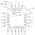
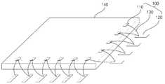
도 1a은 본 발명의 일 실시예에 따른 칩 안테나의 평면도이고, 도 1b는 도 1a의 일부 사시도이다. 도 1b에서는 편의상 도 1a의 좌측과 상측의 패드와 리드 프레임의 도시를 생략하였음을 밝혀둔다. 본 발명에 따른 안테나는 반도체 패키지 내부에 구비되므로 "칩 안테나(chip antenna)"로 명명하기로 한다.1A is a plan view of a chip antenna according to an embodiment of the present invention, and FIG. 1B is a partial perspective view of FIG. 1A. In FIG. 1B, the pads and lead frames on the left side and the upper side of FIG. 1A are omitted for convenience. Since the antenna according to the present invention is provided inside the semiconductor package, it will be referred to as a "chip antenna".
본 발명의 일 실시예에 따른 칩 안테나(100)는, 도 1a 및 도 1b를 참조하면, 반도체 칩(140) 상의 패드(pad)(110), 반도체 칩(140)이 장착되는 기판의 리드 프레임(lead frame)(120) 및 패드(110)와 리드 프레임(120)을 전기적으로 연결하는 와이어(wire)(130)를 포함하여 형성된다.1A and 1B, the
패드(110)는 반도체 칩(140) 상에 복수개 구비된다. 이때, 패드(110) 중 적어도 어느 하나는 반도체 칩(140)의 송신부 또는 수신부(이하, "송수신부")(150)와 전기적으로 연결된다. 또한, 패드(110)와 송수신부(150) 사이에는 파워 앰프(160)가 구비될 수 있음은 물론이다. 패드(110)는 일반적인 반도체 칩의 패드, 즉 반도체 칩과 외부와의 전기적인 연결을 위한 패드(미도시)와는 별도로 형성되며, 그에 따라 일반적인 반도체 칩의 패드와는 다른 역할을 수행한다. 상기 패드(110)는 반 도체 칩에 구비된 여러 소자들을 반도체 칩 외부의 단자들과 전기적으로 연결하는 핀(pin) 역할을 수행하는 것이 아니라, 송수신부(150)와 전기적으로 연결되어 안테나 역할을 수행한다. 그에 따라 핀 역할을 수행하는 패드의 충분한 확보가 문제될 수 있으며, 이에 대해서는 다른 실시예에서 후술하기로 한다. 패드(110)의 표면에는 와이어(130)가 본딩된다.A plurality of
리드 프레임(120)은 반도체 칩(140)이 장착되는 기판(substrate)에 복수개 구비된다. 예컨대, 리드 프레임(120)은 반도체 칩(140)을 둘러싸는 형상으로 배열될 수 있다. 리드 프레임(120)은 패드(110)와 동일한 개수로 형성될 수 있다. 도시되지 않았으나, 리드 프레임은 패드와 다른 개수로 형성될 수도 있으며, 이 경우 리드 프레임끼리 와이어 본딩되거나 패드끼리 와이어 본딩되는 부분이 일부 나타날 수 있다.The
패드(110)와 리드 프레임(120)은 와이어(130)에 의해 전기적으로 연결된다. 일반적으로 반도체 칩의 패드와 리드 프레임을 전기적으로 연결하는 와이어는 전기저항을 감소시키기 위해 금속 재질, 특히 금(Au)으로 형성되나, 상기 와이어(130)는 반도체 칩과 외부 단자와의 연결을 위한 것이 아니므로, 금 이외에도 다양한 금속이 사용될 수 있음은 물론이다.The
이때, 와이어(130)로 패드(110)와 리드 프레임(120)을 연결하는 방식으로는 여러 가지가 가능하다. 도시되지 않았으나, 일부 구간에서는 패드끼리 와이어로 연결되고, 다른 일부 구간에서는 리드 프레임끼리 와이어로 연결될 수도 있다. 최종적인 안테나의 길이를 고려할 때 도 1a에서 보는 바와 같이 와이어(130)는 패 드(110)와 리드 프레임(120)을 번갈아가며 연결하는 것이 바람직하다. 이 경우 최종적인 연결 상태는 패드-와이어-리드 프레임-와이어-패드-...와 같은 배열이 반복되어 직렬로 연결된다. 물론, 도 1a의 우측 상단부와 같이 경우에 따라 리드 프레임끼리 와이어로 연결된 부분이 발생할 수도 있다.In this case, various methods may be used to connect the
패드와 리드 프레임이 동일한 개수로 형성되는 경우, 패드(110)는 제1 패드, 제2 패드, ..., 제n 패드를 포함하고, 리드 프레임(120)은 제1 리드 프레임, 제2 리드 프레임, ..., 제n 리드 프레임을 포함할 수 있다. 이때, 제n 패드는 와이어에 의해 제n 리드 프레임 및 제n-1 리드 프레임과 전기적으로 연결되며, 제n-1 패드는 와이어에 의해 제n-1 리드 프레임 및 제n-2 리드 프레임과 전기적으로 연결될 수 있다(n은 3이상의 유한한 자연수). 예컨대, 도 1a와 같이 n=20 인 경우 제20 패드는 제20 리드 프레임 및 제19 리드 프레임과 연결되고, 제19 패드는 제 19 리드 프레임 및 제18 리드 프레임과 연결될 수 있다.When the pad and the lead frame are formed in the same number, the
이와 같은 방식으로 칩 안테나를 구현할 경우 UWB 통신에 사용하기에 충분한 길이의 안테나를 확보할 수 있다. 특히, 패드와 리드 프레임의 개수를 조절하면 3~5 GHz와 같이 긴 파장을 가지는 주파수 대역에서도 충분히 안테나 역할을 수행할 수 있다.If the chip antenna is implemented in this manner, an antenna of sufficient length to be used for UWB communication can be obtained. In particular, if the number of pads and lead frames is adjusted, the antenna can function sufficiently even in a frequency band having a long wavelength such as 3 to 5 GHz.
다음으로, 본 발명의 다른 실시예에 따른 칩 안테나에 대해 설명한다.Next, a chip antenna according to another embodiment of the present invention will be described.
도 2는 본 발명의 다른 실시예에 따른 칩 안테나의 평면도이다. 도 2의 실시예는 인접하는 패드 사이에 스위치가 구비된 점 이외에는 도 1a의 실시예와 유사하 므로, 차이점을 중심으로 설명한다.2 is a plan view of a chip antenna according to another exemplary embodiment of the present invention. The embodiment of FIG. 2 is similar to the embodiment of FIG. 1A except that the switch is provided between adjacent pads.
본 발명의 다른 실시예에 따른 칩 안테나(200)는, 도 2를 참조하면, 반도체 칩(240) 상의 패드(210), 반도체 칩(240)이 장착되는 기판의 리드 프레임(220), 패드(210)와 리드 프레임(220)을 전기적으로 연결하는 와이어(230) 및 인접하는 패드(210) 사이에 구비된 스위치(270a, 270b, 270c)를 포함하여 형성된다.Referring to FIG. 2, the
칩 안테나(200)는 여러 개의 서브 안테나(sub antenna)로 구분된다. 예컨대, 도 2를 참조하면 칩 안테나(200)는 도 2의 상단부터 시계방향으로 제1 서브 안테나 내지 제4 서브 안테나로 구분될 수 있다. 즉, 칩 안테나(200)는 도 2의 상단에 위치한 제1 서브 안테나, 도 2의 우측에 위치한 제2 서브 안테나, 도 2의 하단에 위치한 제3 서브 안테나, 및 도 2의 좌측에 위치한 제4 서브 안테나로 구성된다. 도 2의 실시예에서는 반도체 칩(240)의 각 변을 기준으로 서브 안테나를 구분함으로써 패드 중 반도체 칩의 엣지(edge)에 위치한 패드 쌍에 스위치가 구비되었으나, 이와 다른 방식으로 서브 안테나를 구성할 수도 있음은 물론이다.The
서브 안테나들 간에는 스위치(270a, 270b, 270c)가 구비된다. 제1 서브 안테나와 제2 서브 안테나 사이에는 제1 스위치(270a), 제2 서브 안테나와 제3 서브 안테나 사이에는 제2 스위치(270b), 제3 서브 안테나와 제4 서브 안테나 사이에는 제3 스위치(270c)가 연결된다. 이때, 제1 스위치(270a)는 제1 서브 안테나를 이루는 패드들 중 시계방향으로 마지막에 위치한 패드와, 제2 서브 안테나를 이루는 패드들 중 시계방향으로 처음에 위치한 패드 사이에 구비될 수 있다. 나머지 스위치들(270b, 270c)도 동일한 방식으로 구비될 수 있다. 이때, 스위치(270a, 270b, 270c)는 소형화와 집적화를 실현하기 위해 트랜지스터와 같은 전자회로로 구현될 수 있으며, 특히 전계효과 트랜지스터(FET)로 구현될 수 있다.
이와 같이 인접하는 적어도 어느 한 쌍의 패드 사이에 스위치를 구비함으로써 칩 안테나의 길이를 조절할 수 있다. 칩 안테나의 길이가 조절되면 다양한 주파수를 가지는 대역에 적응적으로 대응할 수 있다. 예컨대, 특정 주파수 대역을 사용하여 송수신하기 위하여 제1 스위치(270a)를 온(ON) 상태로 함으로써 제1 서브 안테나와 제2 서브 안테나가 전기적으로 연결되도록 한 경우, 이보다 낮은 주파수 대역을 사용하여 송수신하려면 제1 스위치(270a) 및 제2 스위치(270b)을 온(ON) 상태로 하여 제1 서브 안테나 내지 제3 서브 안테나가 전기적으로 연결되도록 하면 된다.Thus, the length of the chip antenna can be adjusted by providing a switch between at least one pair of adjacent pads. When the length of the chip antenna is adjusted, it can adaptively correspond to a band having various frequencies. For example, when the first sub-antenna and the second sub-antenna are electrically connected by turning on the
다음으로, 본 발명의 또 다른 실시예에 따른 칩 안테나에 대해 설명한다.Next, a chip antenna according to another embodiment of the present invention will be described.
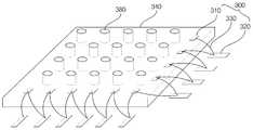
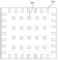
도 3a는 본 발명의 또 다른 실시예에 따른 칩 안테나의 사시도이고, 도 3b는 도 3a의 저면도이다. 도 3b는 편의상 도 3a의 칩 안테나가 봉지재에 의해 패키징 된 상태를 도시하였음을 밝혀둔다. 도 3a의 실시예는 볼그리드어레이(BGA) 형태의 패키징을 위해 비아홀(via hole)이 구비된 점 이외에는 도 1a의 실시예와 유사하므로, 차이점을 중심으로 설명한다. 또한, 도 3a의 실시예에는 도 2의 실시예와 같은 스위치가 선택적으로 적용될 수 있다.3A is a perspective view of a chip antenna according to another exemplary embodiment of the present invention, and FIG. 3B is a bottom view of FIG. 3A. FIG. 3B shows that the chip antenna of FIG. 3A is packaged by an encapsulant for convenience. The embodiment of FIG. 3A is similar to the embodiment of FIG. 1A except that via holes are provided for packaging in a ball grid array (BGA) type, and thus description will be made mainly on differences. In addition, the same switch as the embodiment of FIG. 2 may be selectively applied to the embodiment of FIG. 3A.
본 발명의 또 다른 실시예에 따른 칩 안테나(300)는, 도 3a 및 도 3b를 참조하면, 반도체 칩(340) 상의 패드(310), 반도체 칩(340)이 장착되는 기판의 리드 프 레임(320), 패드(310)와 리드 프레임(320)을 전기적으로 연결하는 와이어(330) 및 반도체 칩(340)을 외부 단자와 연결하기 위한 비아 홀(380)을 포함하여 형성된다.3A and 3B, the
상기에서 언급한 바와 같이 반도체 칩의 패드와 리드 프레임을 안테나로 사용할 경우, 반도체 칩을 외부와 연결하는 연결핀의 충분한 확보가 문제될 수 있다. 이를 위해 도 3a의 실시예에서는 반도체 칩(340)에 다수개의 비아 홀(380)을 형성하고, 이를 이용하여 볼그리드어레이(BGA) 형태의 패키징으로 제조한다. 즉, 반도체 칩(340) 상의 패드(310)는 안테나용으로 이용하고, 외부와 인터커넥션(interconnection)을 위한 패드의 확보를 위해 비아 홀(380)을 사용하여 외부 핀을 만들어 준다. 이때, 도 3b의 반도체 칩 저면에는 솔더볼(solder ball)(미도시)이 용접된다.As mentioned above, when the pad and the lead frame of the semiconductor chip are used as an antenna, sufficient securing of a connection pin connecting the semiconductor chip to the outside may be a problem. To this end, in the embodiment of FIG. 3A, a plurality of via
이와 같이 함으로써 칩 안테나를 위한 패드의 개수를 충분히 확보함과 더불어, 칩 외부와의 전기적 연결을 위한 외부 핀의 개수도 충분히 확보할 수 있게 된다.In this way, the number of pads for the chip antenna is sufficiently secured, and the number of external pins for electrical connection to the outside of the chip can also be sufficiently secured.
다음으로, 본 발명의 또 다른 실시예에 따른 칩 안테나에 대해 설명한다.Next, a chip antenna according to another embodiment of the present invention will be described.
도 4는 본 발명의 또 다른 실시예에 따른 칩 안테나의 사시도이다. 도 4의 실시예는 복수개의 반도체 칩이 적층되어 스택 다이(stack die)를 형성한 점 이외에는 도 3a의 실시예와 유사하므로, 차이점을 중심으로 설명한다. 또한, 도 4의 실시예에서는 도 2의 실시예와 같은 스위치가 선택적으로 적용될 수 있으며, 비아 홀을 구비하지 않은 도 1a의 실시예에 반도체 칩이 추가로 적층되어 스택 다이를 형 성할 수도 있음은 물론이다.4 is a perspective view of a chip antenna according to another embodiment of the present invention. The embodiment of FIG. 4 is similar to the embodiment of FIG. 3A except that a plurality of semiconductor chips are stacked to form a stack die. In addition, in the embodiment of FIG. 4, the same switch as that of the embodiment of FIG. 2 may be selectively applied, and a semiconductor die may be additionally stacked to form a stack die in the embodiment of FIG. 1A having no via hole. Of course.
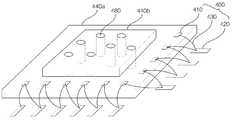
본 발명의 또 다른 실시예에 따른 칩 안테나(400)는, 도 4를 참조하면, 반도체 칩(440a) 상의 패드(410), 반도체 칩(440a)이 장착되는 기판의 리드 프레임(420), 패드(410)와 리드 프레임(420)을 전기적으로 연결하는 와이어(430) 및 반도체 칩(440a)을 외부 단자와 연결하기 위한 비아 홀(480)을 포함하여 형성된다. 이때, 반도체 칩(440a, 440b)은 하부 칩(440a) 상에 상부 칩(440b)이 적층된 상태로 형성된다.Referring to FIG. 4, a
이때, 하부 칩(440a)과 상부 칩(440b) 사이의 전기적인 연결은 비아 홀(480)을 통해 이루어질 수 있다.In this case, electrical connection between the
도 4의 실시예에서는 하부 칩(440a)에 모든 패드(410)가 구비되어 있어, 하부 칩(440a)의 패드(410)가 와이어(430)에 의해 리드 프레임(420)과 전기적으로 연결됨으로써 칩 안테나를 구성한다. 도시되지 않았으나, 상부 칩에도 패드가 구비될 수 있으며, 보다 긴 길이의 칩 안테나를 확보하기 위해 상부 칩에 구비된 패드와 리드 프레임을 와이어로 연결할 수도 있음은 물론이다.In the embodiment of FIG. 4, all the
한편, 본 발명의 바람직한 실시예에 의한 반도체 패키지는 칩 안테나(100, 200, 300, 400)가 위치한 부분을 포함한 소정의 공간에 봉지재(encapsulant)를 사용하여 패키징을 수행함으로써 제조될 수 있다.Meanwhile, the semiconductor package according to an exemplary embodiment of the present invention may be manufactured by packaging using an encapsulant in a predetermined space including a portion where the
또한, 본 발명의 바람직한 실시예에 따른 초광대역(UWB) 통신 시스템은 상기 칩 안테나가 구비된 반도체 패키지로 UWB 무선 송수신 모듈을 구현함으로써 제조될 수 있다. 예컨대, UWB 무선 송수신 모듈은 전파를 방사하거나 흡수하는 칩 안테나, 송수신 전환을 위한 송수신 스위치, 일정 주파수대를 통과시키는 여파기, 고주파 통신용 집적 회로 및 디지털 기저 대역 처리를 위한 집적 회로 등으로 구현될 수 있으며, 여기서 초광대역 통신 시스템의 구성을 한정하는 것은 아니다.In addition, the ultra wideband (UWB) communication system according to a preferred embodiment of the present invention can be manufactured by implementing a UWB wireless transmission and reception module in a semiconductor package equipped with the chip antenna. For example, the UWB wireless transmit / receive module may be implemented as a chip antenna that radiates or absorbs radio waves, a transmit / receive switch for transmitting / receiving switching, a filter passing through a predetermined frequency band, an integrated circuit for high frequency communication, and an integrated circuit for digital baseband processing. The configuration of the ultra-wideband communication system is not limited here.
이와 같이 함으로써 안테나를 포함하는 초소형 통신칩을 이용하여 UWB 통신 시스템을 구현할 수 있게 된다.In this way, it is possible to implement a UWB communication system using a micro communication chip including an antenna.
이상의 설명은 본 발명의 기술 사상을 예시적으로 설명한 것에 불과한 것으로서, 본 발명이 속하는 기술 분야에서 통상의 지식을 가진 자라면 본 발명의 본질적인 특성에서 벗어나지 않는 범위 내에서 다양한 수정, 변경 및 치환이 가능할 것이다. 따라서, 본 발명에 개시된 실시예 및 첨부된 도면들은 본 발명의 기술 사상을 한정하기 위한 것이 아니라 설명하기 위한 것이고, 이러한 실시예 및 첨부된 도면에 의하여 본 발명의 기술 사상의 범위가 한정되는 것은 아니다. 본 발명의 보호 범위는 아래의 청구범위에 의하여 해석되어야 하며, 그와 동등한 범위 내에 있는 모든 기술 사상은 본 발명의 권리범위에 포함되는 것으로 해석되어야 할 것이다.The above description is merely illustrative of the technical idea of the present invention, and various modifications, changes, and substitutions may be made by those skilled in the art without departing from the essential characteristics of the present invention. will be. Accordingly, the embodiments disclosed in the present invention and the accompanying drawings are not intended to limit the technical spirit of the present invention but to describe the present invention, and the scope of the technical idea of the present invention is not limited by the embodiments and the accompanying drawings. . The protection scope of the present invention should be interpreted by the following claims, and all technical ideas within the equivalent scope should be interpreted as being included in the scope of the present invention.
본 발명은 초소형 통신칩 구현을 위해 안테나를 반도체 패키지 내부에 집적함으로써 칩 하나로 통신이 가능하도록 한 바, UWB 통신 시스템을 비롯한 차세대 근거리 통신망 이외에도 초소형 통신 장비를 필요로 하는 다양한 분야에 적용될 수 있다.The present invention is to enable the communication in one chip by integrating the antenna inside the semiconductor package to implement a micro communication chip, it can be applied to various fields that require a micro communication equipment in addition to the next-generation local area network including the UWB communication system.
도 1a은 본 발명의 일 실시예에 따른 칩 안테나의 평면도,1A is a plan view of a chip antenna according to an embodiment of the present invention;
도 1b는 도 1a의 일부 사시도,1B is a partial perspective view of FIG. 1A;
도 2는 본 발명의 다른 실시예에 따른 칩 안테나의 평면도,2 is a plan view of a chip antenna according to another embodiment of the present invention;
도 3a는 본 발명의 또 다른 실시예에 따른 칩 안테나의 사시도,3A is a perspective view of a chip antenna according to another embodiment of the present invention;
도 3b는 도 3b의 저면도,3B is a bottom view of FIG. 3B,
도 4는 본 발명의 또 다른 실시예에 따른 칩 안테나의 사시도이다.4 is a perspective view of a chip antenna according to another embodiment of the present invention.
<도면의 주요 부분에 대한 부호의 설명><Explanation of symbols for the main parts of the drawings>
100, 200, 300, 400 - 칩 안테나100, 200, 300, 400-chip antenna
110, 210, 310, 410 - 패드110, 210, 310, 410-pad
120, 220, 320, 420 - 리드 프레임120, 220, 320, 420-lead frame
130, 230, 330, 430 - 와이어130, 230, 330, 430-wire
270a, 270b, 270c - 스위치270a, 270b, 270c-switch
Claims (14)
Translated fromKoreanPriority Applications (1)
| Application Number | Priority Date | Filing Date | Title |
|---|---|---|---|
| KR1020080018231AKR101014778B1 (en) | 2008-02-28 | 2008-02-28 | Chip antenna and semiconductor package, and ultra-wideband communication system including the same |
Applications Claiming Priority (1)
| Application Number | Priority Date | Filing Date | Title |
|---|---|---|---|
| KR1020080018231AKR101014778B1 (en) | 2008-02-28 | 2008-02-28 | Chip antenna and semiconductor package, and ultra-wideband communication system including the same |
Publications (2)
| Publication Number | Publication Date |
|---|---|
| KR20090092958A KR20090092958A (en) | 2009-09-02 |
| KR101014778B1true KR101014778B1 (en) | 2011-02-14 |
Family
ID=41301489
Family Applications (1)
| Application Number | Title | Priority Date | Filing Date |
|---|---|---|---|
| KR1020080018231AExpired - Fee RelatedKR101014778B1 (en) | 2008-02-28 | 2008-02-28 | Chip antenna and semiconductor package, and ultra-wideband communication system including the same |
Country Status (1)
| Country | Link |
|---|---|
| KR (1) | KR101014778B1 (en) |
Families Citing this family (1)
| Publication number | Priority date | Publication date | Assignee | Title |
|---|---|---|---|---|
| JP2014110555A (en)* | 2012-12-03 | 2014-06-12 | Samsung Electronics Co Ltd | Antenna device |
Citations (2)
| Publication number | Priority date | Publication date | Assignee | Title |
|---|---|---|---|---|
| JP2005182330A (en) | 2003-12-18 | 2005-07-07 | Matsushita Electric Ind Co Ltd | Semiconductor device and manufacturing method of semiconductor device |
| WO2006022836A1 (en)* | 2004-08-06 | 2006-03-02 | International Business Machines Corporation | Apparatus and methods for constructing antennas using wire bonds as radiating elements |
- 2008
- 2008-02-28KRKR1020080018231Apatent/KR101014778B1/ennot_activeExpired - Fee Related
Patent Citations (2)
| Publication number | Priority date | Publication date | Assignee | Title |
|---|---|---|---|---|
| JP2005182330A (en) | 2003-12-18 | 2005-07-07 | Matsushita Electric Ind Co Ltd | Semiconductor device and manufacturing method of semiconductor device |
| WO2006022836A1 (en)* | 2004-08-06 | 2006-03-02 | International Business Machines Corporation | Apparatus and methods for constructing antennas using wire bonds as radiating elements |
Also Published As
| Publication number | Publication date |
|---|---|
| KR20090092958A (en) | 2009-09-02 |
Similar Documents
| Publication | Publication Date | Title |
|---|---|---|
| CN108233974B (en) | Transceiver module | |
| US9923261B2 (en) | Mounting module and antenna apparatus | |
| US10121751B2 (en) | Integrated antennas in wafer level package | |
| US8648454B2 (en) | Wafer-scale package structures with integrated antennas | |
| US10777888B2 (en) | Beamforming integrated circuit with RF grounded material ring | |
| JP5726787B2 (en) | Wireless device, information processing device and storage device provided with the same | |
| KR101639472B1 (en) | Semiconductor devices | |
| WO2006133108A3 (en) | Packaging antennas with integrated circuit chips | |
| JP2013179152A (en) | Wireless device, information processing apparatus comprising the same, and storage device | |
| US20220254730A1 (en) | Signal isolation for module with ball grid array | |
| CN101227024A (en) | Integrated Circuit Antenna Structure | |
| JP6132692B2 (en) | Antenna device | |
| US11715886B2 (en) | Low-cost, IPD and laminate based antenna array module | |
| KR101014778B1 (en) | Chip antenna and semiconductor package, and ultra-wideband communication system including the same | |
| US7352056B2 (en) | Semiconductor package structure with microstrip antennan | |
| US7250673B2 (en) | Signal isolation in a package substrate | |
| KR101133146B1 (en) | Bonding Wire Antenna Communication Module | |
| KR20050065861A (en) | Wireless transceiver module for ultra wide-band | |
| JP6586629B2 (en) | Semiconductor package and semiconductor device | |
| CN111554664A (en) | Signal isolation structure for electromagnetic communication | |
| CN114069204A (en) | RF systems and communication equipment | |
| WO2020200458A1 (en) | Antenna device and method of its fabrication | |
| US9105462B2 (en) | Semiconductor apparatus | |
| KR102605605B1 (en) | Communication module package | |
| KR101129553B1 (en) | Communication Module |
Legal Events
| Date | Code | Title | Description |
|---|---|---|---|
| A201 | Request for examination | ||
| PA0109 | Patent application | St.27 status event code:A-0-1-A10-A12-nap-PA0109 | |
| PA0201 | Request for examination | St.27 status event code:A-1-2-D10-D11-exm-PA0201 | |
| D13-X000 | Search requested | St.27 status event code:A-1-2-D10-D13-srh-X000 | |
| D14-X000 | Search report completed | St.27 status event code:A-1-2-D10-D14-srh-X000 | |
| E902 | Notification of reason for refusal | ||
| PE0902 | Notice of grounds for rejection | St.27 status event code:A-1-2-D10-D21-exm-PE0902 | |
| PG1501 | Laying open of application | St.27 status event code:A-1-1-Q10-Q12-nap-PG1501 | |
| T11-X000 | Administrative time limit extension requested | St.27 status event code:U-3-3-T10-T11-oth-X000 | |
| P11-X000 | Amendment of application requested | St.27 status event code:A-2-2-P10-P11-nap-X000 | |
| P13-X000 | Application amended | St.27 status event code:A-2-2-P10-P13-nap-X000 | |
| E90F | Notification of reason for final refusal | ||
| PE0902 | Notice of grounds for rejection | St.27 status event code:A-1-2-D10-D21-exm-PE0902 | |
| T11-X000 | Administrative time limit extension requested | St.27 status event code:U-3-3-T10-T11-oth-X000 | |
| E13-X000 | Pre-grant limitation requested | St.27 status event code:A-2-3-E10-E13-lim-X000 | |
| P11-X000 | Amendment of application requested | St.27 status event code:A-2-2-P10-P11-nap-X000 | |
| P13-X000 | Application amended | St.27 status event code:A-2-2-P10-P13-nap-X000 | |
| E701 | Decision to grant or registration of patent right | ||
| PE0701 | Decision of registration | St.27 status event code:A-1-2-D10-D22-exm-PE0701 | |
| GRNT | Written decision to grant | ||
| PR0701 | Registration of establishment | St.27 status event code:A-2-4-F10-F11-exm-PR0701 | |
| PR1002 | Payment of registration fee | St.27 status event code:A-2-2-U10-U11-oth-PR1002 Fee payment year number:1 | |
| PG1601 | Publication of registration | St.27 status event code:A-4-4-Q10-Q13-nap-PG1601 | |
| PN2301 | Change of applicant | St.27 status event code:A-5-5-R10-R13-asn-PN2301 St.27 status event code:A-5-5-R10-R11-asn-PN2301 | |
| R18-X000 | Changes to party contact information recorded | St.27 status event code:A-5-5-R10-R18-oth-X000 | |
| PN2301 | Change of applicant | St.27 status event code:A-5-5-R10-R13-asn-PN2301 St.27 status event code:A-5-5-R10-R11-asn-PN2301 | |
| FPAY | Annual fee payment | Payment date:20140128 Year of fee payment:4 | |
| PR1001 | Payment of annual fee | St.27 status event code:A-4-4-U10-U11-oth-PR1001 Fee payment year number:4 | |
| R18-X000 | Changes to party contact information recorded | St.27 status event code:A-5-5-R10-R18-oth-X000 | |
| FPAY | Annual fee payment | Payment date:20150119 Year of fee payment:5 | |
| PR1001 | Payment of annual fee | St.27 status event code:A-4-4-U10-U11-oth-PR1001 Fee payment year number:5 | |
| FPAY | Annual fee payment | Payment date:20160202 Year of fee payment:6 | |
| PR1001 | Payment of annual fee | St.27 status event code:A-4-4-U10-U11-oth-PR1001 Fee payment year number:6 | |
| FPAY | Annual fee payment | Payment date:20170206 Year of fee payment:7 | |
| PR1001 | Payment of annual fee | St.27 status event code:A-4-4-U10-U11-oth-PR1001 Fee payment year number:7 | |
| LAPS | Lapse due to unpaid annual fee | ||
| PC1903 | Unpaid annual fee | St.27 status event code:A-4-4-U10-U13-oth-PC1903 Not in force date:20180209 Payment event data comment text:Termination Category : DEFAULT_OF_REGISTRATION_FEE | |
| PC1903 | Unpaid annual fee | St.27 status event code:N-4-6-H10-H13-oth-PC1903 Ip right cessation event data comment text:Termination Category : DEFAULT_OF_REGISTRATION_FEE Not in force date:20180209 | |
| R18-X000 | Changes to party contact information recorded | St.27 status event code:A-5-5-R10-R18-oth-X000 | |
| PN2301 | Change of applicant | St.27 status event code:A-5-5-R10-R13-asn-PN2301 St.27 status event code:A-5-5-R10-R11-asn-PN2301 |