KR101013473B1 - Semiconductor display device and manufacturing method thereof - Google Patents
Semiconductor display device and manufacturing method thereofDownload PDFInfo
- Publication number
- KR101013473B1 KR101013473B1KR1020030021881AKR20030021881AKR101013473B1KR 101013473 B1KR101013473 B1KR 101013473B1KR 1020030021881 AKR1020030021881 AKR 1020030021881AKR 20030021881 AKR20030021881 AKR 20030021881AKR 101013473 B1KR101013473 B1KR 101013473B1
- Authority
- KR
- South Korea
- Prior art keywords
- film
- insulating film
- opening
- organic resin
- inorganic insulating
- Prior art date
- Legal status (The legal status is an assumption and is not a legal conclusion. Google has not performed a legal analysis and makes no representation as to the accuracy of the status listed.)
- Expired - Fee Related
Links
Images


Classifications
- G—PHYSICS
- G02—OPTICS
- G02F—OPTICAL DEVICES OR ARRANGEMENTS FOR THE CONTROL OF LIGHT BY MODIFICATION OF THE OPTICAL PROPERTIES OF THE MEDIA OF THE ELEMENTS INVOLVED THEREIN; NON-LINEAR OPTICS; FREQUENCY-CHANGING OF LIGHT; OPTICAL LOGIC ELEMENTS; OPTICAL ANALOGUE/DIGITAL CONVERTERS
- G02F1/00—Devices or arrangements for the control of the intensity, colour, phase, polarisation or direction of light arriving from an independent light source, e.g. switching, gating or modulating; Non-linear optics
- G02F1/01—Devices or arrangements for the control of the intensity, colour, phase, polarisation or direction of light arriving from an independent light source, e.g. switching, gating or modulating; Non-linear optics for the control of the intensity, phase, polarisation or colour
- G02F1/13—Devices or arrangements for the control of the intensity, colour, phase, polarisation or direction of light arriving from an independent light source, e.g. switching, gating or modulating; Non-linear optics for the control of the intensity, phase, polarisation or colour based on liquid crystals, e.g. single liquid crystal display cells
- G02F1/133—Constructional arrangements; Operation of liquid crystal cells; Circuit arrangements
- G02F1/136—Liquid crystal cells structurally associated with a semi-conducting layer or substrate, e.g. cells forming part of an integrated circuit
- G02F1/1362—Active matrix addressed cells
- G02F1/136227—Through-hole connection of the pixel electrode to the active element through an insulation layer
- H—ELECTRICITY
- H10—SEMICONDUCTOR DEVICES; ELECTRIC SOLID-STATE DEVICES NOT OTHERWISE PROVIDED FOR
- H10D—INORGANIC ELECTRIC SEMICONDUCTOR DEVICES
- H10D86/00—Integrated devices formed in or on insulating or conducting substrates, e.g. formed in silicon-on-insulator [SOI] substrates or on stainless steel or glass substrates
- H10D86/40—Integrated devices formed in or on insulating or conducting substrates, e.g. formed in silicon-on-insulator [SOI] substrates or on stainless steel or glass substrates characterised by multiple TFTs
- H10D86/441—Interconnections, e.g. scanning lines
- H10D86/443—Interconnections, e.g. scanning lines adapted for preventing breakage, peeling or short circuiting
- H—ELECTRICITY
- H10—SEMICONDUCTOR DEVICES; ELECTRIC SOLID-STATE DEVICES NOT OTHERWISE PROVIDED FOR
- H10D—INORGANIC ELECTRIC SEMICONDUCTOR DEVICES
- H10D86/00—Integrated devices formed in or on insulating or conducting substrates, e.g. formed in silicon-on-insulator [SOI] substrates or on stainless steel or glass substrates
- H10D86/40—Integrated devices formed in or on insulating or conducting substrates, e.g. formed in silicon-on-insulator [SOI] substrates or on stainless steel or glass substrates characterised by multiple TFTs
- H10D86/451—Integrated devices formed in or on insulating or conducting substrates, e.g. formed in silicon-on-insulator [SOI] substrates or on stainless steel or glass substrates characterised by multiple TFTs characterised by the compositions or shapes of the interlayer dielectrics
- H—ELECTRICITY
- H10—SEMICONDUCTOR DEVICES; ELECTRIC SOLID-STATE DEVICES NOT OTHERWISE PROVIDED FOR
- H10D—INORGANIC ELECTRIC SEMICONDUCTOR DEVICES
- H10D86/00—Integrated devices formed in or on insulating or conducting substrates, e.g. formed in silicon-on-insulator [SOI] substrates or on stainless steel or glass substrates
- H10D86/40—Integrated devices formed in or on insulating or conducting substrates, e.g. formed in silicon-on-insulator [SOI] substrates or on stainless steel or glass substrates characterised by multiple TFTs
- H10D86/481—Integrated devices formed in or on insulating or conducting substrates, e.g. formed in silicon-on-insulator [SOI] substrates or on stainless steel or glass substrates characterised by multiple TFTs integrated with passive devices, e.g. auxiliary capacitors
- H—ELECTRICITY
- H10—SEMICONDUCTOR DEVICES; ELECTRIC SOLID-STATE DEVICES NOT OTHERWISE PROVIDED FOR
- H10D—INORGANIC ELECTRIC SEMICONDUCTOR DEVICES
- H10D86/00—Integrated devices formed in or on insulating or conducting substrates, e.g. formed in silicon-on-insulator [SOI] substrates or on stainless steel or glass substrates
- H10D86/40—Integrated devices formed in or on insulating or conducting substrates, e.g. formed in silicon-on-insulator [SOI] substrates or on stainless steel or glass substrates characterised by multiple TFTs
- H10D86/60—Integrated devices formed in or on insulating or conducting substrates, e.g. formed in silicon-on-insulator [SOI] substrates or on stainless steel or glass substrates characterised by multiple TFTs wherein the TFTs are in active matrices
- H—ELECTRICITY
- H10—SEMICONDUCTOR DEVICES; ELECTRIC SOLID-STATE DEVICES NOT OTHERWISE PROVIDED FOR
- H10D—INORGANIC ELECTRIC SEMICONDUCTOR DEVICES
- H10D86/00—Integrated devices formed in or on insulating or conducting substrates, e.g. formed in silicon-on-insulator [SOI] substrates or on stainless steel or glass substrates
- H10D86/80—Integrated devices formed in or on insulating or conducting substrates, e.g. formed in silicon-on-insulator [SOI] substrates or on stainless steel or glass substrates characterised by multiple passive components, e.g. resistors, capacitors or inductors
- H—ELECTRICITY
- H10—SEMICONDUCTOR DEVICES; ELECTRIC SOLID-STATE DEVICES NOT OTHERWISE PROVIDED FOR
- H10H—INORGANIC LIGHT-EMITTING SEMICONDUCTOR DEVICES HAVING POTENTIAL BARRIERS
- H10H20/00—Individual inorganic light-emitting semiconductor devices having potential barriers, e.g. light-emitting diodes [LED]
- H10H20/80—Constructional details
- H10H20/85—Packages
- H10H20/852—Encapsulations
- H—ELECTRICITY
- H10—SEMICONDUCTOR DEVICES; ELECTRIC SOLID-STATE DEVICES NOT OTHERWISE PROVIDED FOR
- H10K—ORGANIC ELECTRIC SOLID-STATE DEVICES
- H10K50/00—Organic light-emitting devices
- H10K50/80—Constructional details
- H10K50/84—Passivation; Containers; Encapsulations
- H—ELECTRICITY
- H10—SEMICONDUCTOR DEVICES; ELECTRIC SOLID-STATE DEVICES NOT OTHERWISE PROVIDED FOR
- H10K—ORGANIC ELECTRIC SOLID-STATE DEVICES
- H10K59/00—Integrated devices, or assemblies of multiple devices, comprising at least one organic light-emitting element covered by group H10K50/00
- H10K59/10—OLED displays
- H10K59/12—Active-matrix OLED [AMOLED] displays
- H10K59/122—Pixel-defining structures or layers, e.g. banks
- H—ELECTRICITY
- H10—SEMICONDUCTOR DEVICES; ELECTRIC SOLID-STATE DEVICES NOT OTHERWISE PROVIDED FOR
- H10K—ORGANIC ELECTRIC SOLID-STATE DEVICES
- H10K59/00—Integrated devices, or assemblies of multiple devices, comprising at least one organic light-emitting element covered by group H10K50/00
- H10K59/10—OLED displays
- H10K59/12—Active-matrix OLED [AMOLED] displays
- H10K59/123—Connection of the pixel electrodes to the thin film transistors [TFT]
- H—ELECTRICITY
- H10—SEMICONDUCTOR DEVICES; ELECTRIC SOLID-STATE DEVICES NOT OTHERWISE PROVIDED FOR
- H10K—ORGANIC ELECTRIC SOLID-STATE DEVICES
- H10K59/00—Integrated devices, or assemblies of multiple devices, comprising at least one organic light-emitting element covered by group H10K50/00
- H10K59/10—OLED displays
- H10K59/12—Active-matrix OLED [AMOLED] displays
- H10K59/124—Insulating layers formed between TFT elements and OLED elements
- H—ELECTRICITY
- H10—SEMICONDUCTOR DEVICES; ELECTRIC SOLID-STATE DEVICES NOT OTHERWISE PROVIDED FOR
- H10K—ORGANIC ELECTRIC SOLID-STATE DEVICES
- H10K59/00—Integrated devices, or assemblies of multiple devices, comprising at least one organic light-emitting element covered by group H10K50/00
- H10K59/10—OLED displays
- H10K59/12—Active-matrix OLED [AMOLED] displays
- H10K59/131—Interconnections, e.g. wiring lines or terminals
- G—PHYSICS
- G02—OPTICS
- G02F—OPTICAL DEVICES OR ARRANGEMENTS FOR THE CONTROL OF LIGHT BY MODIFICATION OF THE OPTICAL PROPERTIES OF THE MEDIA OF THE ELEMENTS INVOLVED THEREIN; NON-LINEAR OPTICS; FREQUENCY-CHANGING OF LIGHT; OPTICAL LOGIC ELEMENTS; OPTICAL ANALOGUE/DIGITAL CONVERTERS
- G02F1/00—Devices or arrangements for the control of the intensity, colour, phase, polarisation or direction of light arriving from an independent light source, e.g. switching, gating or modulating; Non-linear optics
- G02F1/01—Devices or arrangements for the control of the intensity, colour, phase, polarisation or direction of light arriving from an independent light source, e.g. switching, gating or modulating; Non-linear optics for the control of the intensity, phase, polarisation or colour
- G02F1/13—Devices or arrangements for the control of the intensity, colour, phase, polarisation or direction of light arriving from an independent light source, e.g. switching, gating or modulating; Non-linear optics for the control of the intensity, phase, polarisation or colour based on liquid crystals, e.g. single liquid crystal display cells
- G02F1/133—Constructional arrangements; Operation of liquid crystal cells; Circuit arrangements
- G02F1/1333—Constructional arrangements; Manufacturing methods
- G02F1/133357—Planarisation layers
- H—ELECTRICITY
- H10—SEMICONDUCTOR DEVICES; ELECTRIC SOLID-STATE DEVICES NOT OTHERWISE PROVIDED FOR
- H10K—ORGANIC ELECTRIC SOLID-STATE DEVICES
- H10K50/00—Organic light-emitting devices
- H10K50/80—Constructional details
- H10K50/84—Passivation; Containers; Encapsulations
- H10K50/844—Encapsulations
- H—ELECTRICITY
- H10—SEMICONDUCTOR DEVICES; ELECTRIC SOLID-STATE DEVICES NOT OTHERWISE PROVIDED FOR
- H10K—ORGANIC ELECTRIC SOLID-STATE DEVICES
- H10K59/00—Integrated devices, or assemblies of multiple devices, comprising at least one organic light-emitting element covered by group H10K50/00
- H10K59/80—Constructional details
- H10K59/87—Passivation; Containers; Encapsulations
- H10K59/873—Encapsulations
Landscapes
- Physics & Mathematics (AREA)
- Microelectronics & Electronic Packaging (AREA)
- Engineering & Computer Science (AREA)
- Nonlinear Science (AREA)
- Optics & Photonics (AREA)
- Mathematical Physics (AREA)
- Crystallography & Structural Chemistry (AREA)
- General Physics & Mathematics (AREA)
- Chemical & Material Sciences (AREA)
- Thin Film Transistor (AREA)
- Electroluminescent Light Sources (AREA)
- Liquid Crystal (AREA)
- Devices For Indicating Variable Information By Combining Individual Elements (AREA)
- Formation Of Insulating Films (AREA)
Abstract
Translated fromKorean
Description
Translated fromKorean도 1(A)∼도 1(D)는 개구부에서의 감광성 아크릴막의 단면도,1A to 1D are cross-sectional views of the photosensitive acrylic film in the openings,
도 2는 개구부에서의 감광성 포지티브형 폴리이미드막의 단면도,2 is a cross-sectional view of the photosensitive positive polyimide film in the opening;
도 3(A)∼도 3(C)는 콘택트 홀의 단면도,3 (A) to 3 (C) are cross-sectional views of a contact hole,
도 4(A)∼도 4(D)는 콘택트 홀과 배선과의 위치 관계를 나타내는 도면,4 (A) to 4 (D) are views showing the positional relationship between contact holes and wirings;
도 5(A) 및 도 5(B)는 본 발명의 반도체 표시장치에 포함되는 TFT 및 보유 용량의 단면도,5A and 5B are cross-sectional views of TFTs and storage capacitors included in the semiconductor display device of the present invention;
도 6(A) 및 도 6(B)는 본 발명의 반도체 표시장치의 구동회로의 블록도 및 회로도,6A and 6B are a block diagram and a circuit diagram of a driving circuit of the semiconductor display device of the present invention;
도 7(A) 및 도 7(B)는 승압 회로의 마스크 도면 및 회로도,7 (A) and 7 (B) show a mask diagram and a circuit diagram of a boost circuit;
도 8(A)∼도 8(C)는 본 발명의 반도체 표시장치의 제조방법을 나타내는 도면,8A to 8C show a method of manufacturing a semiconductor display device of the present invention;
도 9(A)∼도 9(C)는 본 발명의 반도체 표시장치의 제조방법을 나타내는 도면,9A to 9C are views showing a method for manufacturing a semiconductor display device of the present invention;
도 10(A)∼도 10(C)는 본 발명의 반도체 표시장치의 제조방법을 나타내는 도면,10A to 10C are views showing a method for manufacturing a semiconductor display device of the present invention;
도 11(A)∼도 11(C)는 본 발명의 반도체 표시장치의 제조방법을 나타내는 도면,11A to 11C are views showing a method for manufacturing a semiconductor display device of the present invention;
도 12(A) 및 도 12(B)는 본 발명의 반도체 표시장치의 제조방법을 나타내는 도면,12A and 12B show a method of manufacturing a semiconductor display device of the present invention;
도 13(A)∼도 13(D)는 본 발명의 반도체 표시장치의 단면도,13A to 13D are cross-sectional views of the semiconductor display device of the present invention;
도 14(A) 및 도 14(B)는 본 발명의 반도체 표시장치의 단면도,14A and 14B are cross-sectional views of the semiconductor display device of the present invention;
도 15(A) 및 도 15(B)는 본 발명의 반도체 표시장치의 제조방법을 나타내는 도면,15A and 15B show a method of manufacturing a semiconductor display device of the present invention;
도 16은 본 발명의 반도체 표시장치의 상면도,16 is a top view of the semiconductor display device of the present invention;
도 17은 발광장치의 콘트롤러의 구성을 나타내는 블록도,17 is a block diagram showing a configuration of a controller of the light emitting device;
도 18은 본 발명의 반도체 표시장치의 단면도,18 is a cross-sectional view of a semiconductor display device of the present invention;
도 19(A) 및 도 19(B)는 각각 본 발명의 반도체 표시장치의 구동회로의 블록도 및 회로도,19A and 19B are respectively a block diagram and a circuit diagram of a drive circuit of the semiconductor display device of the present invention;
도 20(A) 및 도 20(B)는 본 발명의 반도체 표시장치에 포함되는 CPU 및 ASIC의 구성을 나타내는 블록도,20A and 20B are block diagrams showing the configuration of a CPU and an ASIC included in the semiconductor display device of the present invention;
도 21은 본 발명의 반도체 표시장치의 단면도,21 is a cross-sectional view of a semiconductor display device of the present invention;
도 22(A)∼도 22(H)는 본 발명의 반도체 표시장치를 이용하는 전자 기기를 나타내는 도면,22A to 22H are views showing electronic devices using the semiconductor display device of the present invention;
도 23은 본 발명의 반도체 표시장치에 포함되는 승압 회로의 회로도,23 is a circuit diagram of a boost circuit included in a semiconductor display device of the present invention;
도 24는 TFT의 채널 길이와 스레시홀드값의 관계를 나타내는 도면,24 is a diagram showing a relationship between a channel length and a threshold value of a TFT;
도 25(A) 및 도 25(B)는 TFT의 CV 특성을 나타내는 그래프,25 (A) and 25 (B) are graphs showing CV characteristics of TFTs;
도 26(A) 및 도 26(B)는 개구부에서의 비감광성 아크릴막의 단면도,26A and 26B are cross-sectional views of the non-photosensitive acrylic film in the openings,
도 27(A) 및 도 27(B)는 개구부에서의 감광성 포지티브형 아크릴막의 단면도,27A and 27B are cross-sectional views of the photosensitive positive acrylic film in the opening;
도 28(A) 및 도 28(B)는 개구부에서의 감광성 네거티브형 아크릴막의 단면도,28A and 28B are cross-sectional views of the photosensitive negative acrylic film in the opening;
도 29(A) 및 도 29(B)는 개구부에서의 감광성 포지티브형 폴리이미드막의 단면도.29 (A) and 29 (B) are cross-sectional views of the photosensitive positive polyimide film in the opening.
* 도면의 주요 부분에 대한 부호의 설명* Explanation of symbols for the main parts of the drawings
8000: 절연면8001: TFT8000: insulation surface 8001: TFT
8002: 반도체막8003: 게이트 절연막8002: semiconductor film 8003: gate insulating film
8004: 게이트 전극8005: 채널 형성 영역8004: gate electrode 8005: channel formation region
8006: 불순물 영역8007: 용량용 제1 전극8006: impurity region 8007: first electrode for capacitance
8008: 제1 무기 절연막8009: 유기 수지막8008: first inorganic insulating film 8009: organic resin film
8010: 제2 무기 절연막8011: 배선8010: second inorganic insulating film 8011: wiring
8012: 용량용 제2 전극8013: 보유 용량8012: second electrode for capacitance 8013: retention capacitance
본 발명은 층간절연막으로서 유기 수지막을 사용한 반도체 표시장치에 관한 것이다.The present invention relates to a semiconductor display device using an organic resin film as an interlayer insulating film.
근년, 기판 상에 TFT를 형성하는 기술은 큰 발전을 이루었고, 이러한 기술을 반도체장치의 하나인 액티브 매트릭스형 표시장치에 응용하는 기술도 진전이 있어 왔다. 특히, 다결정 반도체막을 사용한 TFT는 비정질 반도체막을 사용한 종래의 TFT에 비해 전계효과 이동도가 높기 때문에 고속동작이 가능하다. 이에 따라, 종래에 기판의 외부에 제공된 구동회로에 의해 행해지던 화소의 제어를, 화소가 형성된 기판과 동일한 기판 상에 형성된 구동회로로 행하는 것이 가능하다.In recent years, the technology of forming a TFT on a substrate has made great progress, and the technology of applying such a technology to an active matrix display device, which is one of semiconductor devices, has progressed. In particular, since the TFT using the polycrystalline semiconductor film has a higher field effect mobility than the conventional TFT using the amorphous semiconductor film, high-speed operation is possible. Thereby, it is possible to control the pixel conventionally performed by the drive circuit provided outside the board | substrate by the drive circuit formed on the same board | substrate as the board | substrate with which the pixel was formed.
TFT는, 반도체막에 일 도전형을 부여하는 불순물을 첨가하여 얻어지는 활성층과, 게이트 전극과, 그 활성층과 게이트 전극 사이에 형성된 게이트 절연막을 포함하고 있다. 또한, 일반적으로, 절연막으로 이루어진 층간절연막이 TFT를 덮도록 형성되고, 그 층간절연막 상에는 TFT에 전기적으로 접속되는 배선이 형성된다.The TFT includes an active layer obtained by adding an impurity imparting one conductivity type to a semiconductor film, a gate electrode, and a gate insulating film formed between the active layer and the gate electrode. In general, an interlayer insulating film made of an insulating film is formed so as to cover the TFT, and a wiring electrically connected to the TFT is formed on the interlayer insulating film.
TFT에 전기적으로 접속되는 배선을 층간절연막 상에 형성할 때, 그 층간절연막의 표면이 충분히 평탄화되어 있지 않으면, 배선의 단선이 유발되거나, 또는 배선이 일부에서 얇게 되어 배선 저항이 증가하게 된다. 또한, 층간절연막 상에 화소 전극이 형성되는 경우에는, 층간절연막의 표면의 요철로 인해 화소 전극의 표면에 요철이 형성되거나, 화소 전극의 두께가 균일하게 될 수 없게 되어, 표시 불균일이 발생하게 된다.When the wiring electrically connected to the TFT is formed on the interlayer insulating film, if the surface of the interlayer insulating film is not sufficiently flattened, disconnection of the wiring is caused, or the wiring becomes thin in part, thereby increasing the wiring resistance. In addition, when the pixel electrode is formed on the interlayer insulating film, irregularities are formed on the surface of the pixel electrode due to the unevenness of the surface of the interlayer insulating film, or the thickness of the pixel electrode cannot be uniform, resulting in display unevenness. .
따라서, TFT 특유의 형상에 따라 층간절연막의 표면에 요철이 나타나는 것을 방지하기 위해 층간절연막을 충분히 두껍게, 예를 들어, 1∼5 ㎛ 정도의 두께로 형성하는 것이 필요하다.Therefore, it is necessary to form the interlayer insulating film sufficiently thick, for example, in a thickness of about 1 to 5 mu m, in order to prevent the unevenness from appearing on the surface of the interlayer insulating film according to the shape peculiar to the TFT.
층간절연막은 크게 나누어, 무기 절연막(이하, 무기 수지막이라 칭함)과, 절연성을 가지고 있는 유기 수지로 이루어진 절연막(이하, 유기 수지막이라 칭함)으로 분류된다.The interlayer insulating film is broadly divided into an inorganic insulating film (hereinafter referred to as an inorganic resin film) and an insulating film made of an organic resin having an insulating property (hereinafter referred to as an organic resin film).
무기 절연막은 CVD법 또는 스퍼터링법 등의 기상 성장법에 의해 형성된다. 따라서, 층간절연막으로서 무기 절연막을 사용하는 경우에는, 무기 절연막을 그의 표면이 평탄화되기에 충분히 두껍게 형성하여야 하기 때문에, 처리에 시간이 걸리는 단점이 있다.The inorganic insulating film is formed by a vapor phase growth method such as CVD method or sputtering method. Therefore, in the case of using the inorganic insulating film as the interlayer insulating film, the inorganic insulating film must be formed thick enough so that its surface is flattened, so that the processing takes time.
한편, 유기 수지막을 사용하는 경우에는, TFT가 형성되는 기판에 유기 수지를 도포할 수 있기 때문에, 표면이 평탄화된 층간절연막을 용이하게 형성할 수 있다.On the other hand, when using an organic resin film, since an organic resin can be apply | coated to the board | substrate in which TFT is formed, an interlayer insulation film with a flat surface can be formed easily.
또한, 콘택트 홀이 개구되어 있는 층간절연막 상에 도전성을 가지는 막(이하, 도전막이라 칭함)을 형성한 후, 그 도전막을 에칭함으로써, TFT에 접속되는 배선을 형성한다.Further, after forming a conductive film (hereinafter referred to as a conductive film) on the interlayer insulating film in which the contact hole is opened, the conductive film is etched to form a wiring connected to the TFT.
이 경우, 도전막의 에칭으로서, 습식 에칭과 건식 에칭 모두를 사용할 수 있다. 그러나, 습식 에칭은 등방성 에칭이므로 3 ㎛ 이하의 배선 패턴의 미세화에 대처할 수 없다. 한편, 건식 에칭은 이방성 에칭이 가능하므로 배선 패턴의 미세화에 대처가 가능하다.In this case, both wet etching and dry etching can be used as the etching of the conductive film. However, since wet etching is isotropic etching, it cannot cope with refinement | miniaturization of the wiring pattern of 3 micrometers or less. On the other hand, dry etching is anisotropic etching is possible, it is possible to cope with the miniaturization of the wiring pattern.
그러나, 건식 에칭의 문제점은, 유기 수지막으로 이루어진 층간절연막 상에 도전막을 형성할 때 그 유기 수지막의 표면이 거칠어진다는 것이다. 유기 수지막의 표면이 거칠어지면, 유기 수지막 상에 형성되는 화소 전극의 표면의 평탄성이 손상되고, 그것이 화소에서의 표시에 영향을 미친다.However, a problem of dry etching is that the surface of the organic resin film becomes rough when a conductive film is formed on an interlayer insulating film made of an organic resin film. If the surface of the organic resin film becomes rough, the flatness of the surface of the pixel electrode formed on the organic resin film is impaired, which affects the display in the pixel.
또한, 유기 수지는 흡수성이 높고, 현상에서 사용되는 알칼리성 수용액 중의 수분을 흡수하여 습윤된다. 따라서, 현상 후 유기 수지막을 가열 처리하는 공정을 제공하여, 유기 수지막에 함유된 수분을 증발시키는 것이 필요하다. 그러나, 유기 수지막을 가열 처리하여 수분을 증발시키더라도, 이 막은 인접 막 또는 대기로부터 수분을 흡수하기 쉽고, 그 막 중의 수분이 유기 수지막에 접하여 형성된 배선을 시간 경과에 따라 부식시켜, 패널의 장기 신뢰성을 손상시킨다.In addition, the organic resin is highly absorbent and absorbs and wets the moisture in the alkaline aqueous solution used in development. Therefore, it is necessary to provide the process of heat-processing an organic resin film after image development, and to evaporate the moisture contained in the organic resin film. However, even if the organic resin film is heat-treated to evaporate moisture, the film tends to absorb moisture from the adjacent film or the atmosphere, and the moisture in the film corrodes the wiring formed in contact with the organic resin film over time, thereby prolonging the panel's long term. Impair reliability.
본 발명은 상기한 단점 및 다른 단점을 감안하여 이루어진 것으로, 본 발명의 목적은, 성막시간을 억제하면서 층간절연막의 표면의 평탄성을 얻을 수 있고, 층간절연막 내의 수분을 제거하기 위한 가열 처리의 처리 시간을 억제할 수 있고, 층간절연막에 인접한 막 또는 전극으로 수분이 방출되는 것을 방지할 수 있는 층간절연막을 가지는 반도체 표시장치를 제공하는데 있다.SUMMARY OF THE INVENTION The present invention has been made in view of the above and other disadvantages, and an object of the present invention is to obtain flatness of the surface of an interlayer insulating film while suppressing the film formation time, and to process the heat treatment for removing moisture in the interlayer insulating film. The present invention provides a semiconductor display device having an interlayer insulating film capable of suppressing and preventing moisture from being released to a film or an electrode adjacent to the interlayer insulating film.
또한, 박막트랜지스터를 포함하는 회로는 표면 상에 어느 정도의 요철을 가지고 있기 때문에, 그 위에 액정 소자 또는 발광 소자를 형성하는데 있어 유기 수지막 등으로 표면을 평탄화시키는 것이 일반적으로 행해지고 있다. 그러나, 본 출원인의 연구에 의하면, 다음과 같은 사실이 판명되었다. 즉, 층간절연막으로서 수지막을 사용하고 건식 에칭 기술을 이용하여 콘택트 홀을 형성하는 경우, 완성된 박막트랜지스터의 스레시홀드 전압(Vth)이 크게 변동한다는 사실이 판명되었다. 예를 들어, 도 24(A) 및 도 24(B)에 나타낸 데이터는, SOI 기판 상에 형성된 박막트랜지스터의 스레시홀드 전압의 변동을 시험한 결과이다. 이들 도면에서, 검은색 원은 층간절연막으로서 질화규소(SiN)막과 아크릴막의 적층 구조를 사용한 경우를 나타내고, 흰색 삼각형은 층간절연막으로서 질화산화규소(SiNO)막과 산화질화규소(SiON)막의 적층 구조를 사용한 경우를 나타낸다. 또한, 양 경우 모두, 콘택트 홀의 개구에 건식 에칭 기술을 사용하였다. 여기서, "SiNO"와 "SiON"의 표기의 차이는, 전자(前者)는 산소보다 질소를 더 많이 함유하고, 후자는 질소보다 산소를 더 많이 함유한다는 의미로 구분된다.In addition, since a circuit including a thin film transistor has a certain degree of irregularities on the surface, in forming a liquid crystal element or a light emitting element thereon, flattening the surface with an organic resin film or the like is generally performed. However, according to the applicant's research, the following facts were found. In other words, it was found that when the resin film was used as the interlayer insulating film and the contact hole was formed using the dry etching technique, the threshold voltage Vth of the completed thin film transistor greatly varied. For example, the data shown in FIGS. 24A and 24B are the results of testing variations in the threshold voltage of the thin film transistor formed on the SOI substrate. In these figures, the black circles indicate the case where the silicon nitride (SiN) film and the acrylic film are laminated as the interlayer insulating film, and the white triangles show the silicon nitride oxide (SiNO) film and the silicon oxynitride (SiON) film as the interlayer insulating film. The case used is shown. Also, in both cases, dry etching techniques were used for the openings of the contact holes. Here, the difference between the notation of "SiNO" and "SiON" is distinguished by the meaning that the former contains more nitrogen than oxygen, and the latter contains more oxygen than nitrogen.
도 24(A) 및 도 24(B)의 데이터는 스레시홀드 전압의 변동을 통계 처리에 따라 평가한 그래프이고, 수평축은 채널 길이(캐리어 이동 길이)를 나타내고, 수직축은 Vth의 변동을 나타낸다. 통계 처리로서는, "4분위 편차"(Quartile deviation)가 알려져 있다. 4분위 편차는 정규 확률 그래프에서의 25%의 값과 75%의 값과의 차이고, 이상치(abnormal value)에 의해 영향을 받지 않는 통계 처리로서 주목을 받고 있다. 본 출원인은 이러한 4분위 편차(25% 편차라고도 함)에 의거하여 16%의 값과 84%의 값과의 차를 16% 분위 편차로서 정의하고, 그 값을 "Vth 편차"로서 수직축에 플로트(plot)하고 있다. 또한, 16% 분위 편차는 정규 확률 분포에서 말하는 ±σ에 상당하기 때문에, 각각 계수를 곱하고, ±3σ로서 간주될 수 있는 값으로 변경한 값들을 데이터 플로트에 사용하고 있다. 이 데이터만으로 판단하면, 층간절연막으로서 아크릴막을 사용한 n채널형 TFT와 p채널형 TFT는 층간절연막으로서 SiNO막과 SiON막을 사용한 것들에 비해 변동이 각각 4배 및 2배 정도 더 크다. 아크릴막을 사용한 경우 변동이 더 크다는 것이 명백하다. 본 출원인은, 건식 에칭시의 플라즈마 데미지(damage)로 인해 아크릴막이 전하를 포획하게 되고, 그 결과로서 스레시홀드 전압의 변동이 나타나는 것은 아닌가 추측하고 있다.24A and 24B are graphs in which the variation of the threshold voltage is evaluated in accordance with statistical processing, the horizontal axis representing the channel length (carrier moving length), and the vertical axis representing the variation of Vth. As a statistical process, "Quartile deviation" is known. The quartile deviation is the difference between the value of 25% and the value of 75% in the normal probability graph, and is drawing attention as a statistical process that is not affected by an abnormal value. Based on this quartile deviation (also known as 25% deviation), we define the difference between the 16% value and the 84% value as the 16% quartile deviation, and define the value as a "Vth deviation" on the vertical axis as a "Vth deviation". plot). In addition, since the 16% quantile deviation corresponds to ± σ in the normal probability distribution, the values are multiplied by coefficients and changed to values that can be regarded as ± 3σ, and used in the data plot. Judging from this data alone, the n-channel TFT and the p-channel TFT using the acrylic film as the interlayer insulating film are four times and twice as large as those compared to those using the SiNO film and SiON film as the interlayer insulating film, respectively. It is clear that the variation is larger when an acrylic film is used. Applicants speculate that the acrylic film traps charge due to plasma damage during dry etching, and as a result, fluctuations in the threshold voltage appear.
본 발명은 상기 문제를 감안하여 이루어진 것으로, 본 발명의 목적은, 층간절연막으로서 유기 수지막을 사용한 표시장치를 제조하는데 있어서 박막트랜지스터를 그의 스레시홀드 전압의 변동없이 제조하는 기술을 제공하여, 표시장치의 동작 성능의 안정성의 향상, 및 회로 설계에 있어서의 설계 마진(margin)의 확대를 달성하는데 있다. 또한, 본 발명의 다른 목적은, 표시장치의 화질의 향상을 달성하는데 있다.SUMMARY OF THE INVENTION The present invention has been made in view of the above problems, and an object of the present invention is to provide a technique for manufacturing a thin film transistor without changing its threshold voltage in manufacturing a display device using an organic resin film as an interlayer insulating film. To achieve an improvement in the stability of the operating performance and to increase the design margin in the circuit design. Another object of the present invention is to achieve an improvement in image quality of a display device.
본 발명에서는, 포지티브형 감광성 아크릴 수지를 포함하는 유기 수지막의 둘레를 유기 수지에 비해 수분을 투과시키기 어려운 질소 함유 절연막으로 에워싸도록 하였다.In the present invention, the periphery of the organic resin film containing the positive photosensitive acrylic resin is surrounded by a nitrogen-containing insulating film that is less likely to transmit moisture than the organic resin.
구체적으로는, TFT를 형성한 후, 이 TFT를 덮도록, 유기 수지에 비해 수분을 투과시키기 어려운 질소 함유 무기 절연막을 형성한다. 그 다음, 이 무기 절연막에, 감광성 아크릴 수지를 포함하는 유기 수지를 도포하여 유기 수지막을 형성하고, 이 유기 수지막을 부분적으로 노광하여 개구시킨다. 그 후, 개구된 유기 수지막을 덮도록, 유기 수지에 비해 수분을 투과시키기 어려운 질소 함유 무기 절연막을 형성하고, 이어서, 유기 수지막의 개구부에서, 게이트 절연막과 질소를 함유하는 2층 무기 절연막을 에칭하여 부분적으로 개구시킴으로써, TFT의 활성층을 노출시킨다.Specifically, after forming the TFT, a nitrogen-containing inorganic insulating film is formed so as to cover the TFT so that moisture is less likely to pass through than the organic resin. Next, an organic resin containing photosensitive acrylic resin is applied to the inorganic insulating film to form an organic resin film, and the organic resin film is partially exposed to open. Thereafter, a nitrogen-containing inorganic insulating film that is less likely to permeate moisture than an organic resin is formed so as to cover the opened organic resin film, and then, the gate insulating film and the two-layer inorganic insulating film containing nitrogen are etched through the opening of the organic resin film. By partially opening, the active layer of the TFT is exposed.
이 에칭 시에, 후의 공정에서 표면에 배선 또는 화소 전극과 같은, 수분의 영향 및 막 표면의 요철의 영향을 회피하는 것이 바람직한 부분이 형성되는 영역에서 유기 수지막이 노출되는 것을 방지하는 것이 필수이다. 또한, 그 외의 영역은 무기 절연막으로 완전히 덮일 수도 있다.At the time of this etching, it is essential to prevent the exposure of the organic resin film in a region where a portion where it is desirable to avoid the influence of moisture, such as wiring or pixel electrodes, and the unevenness of the film surface on the surface is formed in a later step. Further, other regions may be completely covered with the inorganic insulating film.
일반적으로, 무기 절연막은 아크릴 수지로 대표되는 유기 수지막에 비해 건식 에칭으로 인한 에칭 데미지가 적기 때문에, 막 표면의 거치름(roughness)이 적다. 따라서, 후에 형성되는 화소 전극 등의 표면 상에 요철이 나타나는 것이 방지되거나, 화소 전극의 두께가 불균일하게 되는 것이 방지되기 때문에, 표시 시에 불균일이 발생하는 것이 방지될 수 있다.In general, the inorganic insulating film has less etching damage due to dry etching than the organic resin film represented by the acrylic resin, and therefore, the roughness of the film surface is small. Therefore, since irregularities are prevented from appearing on the surface of the pixel electrode or the like formed later, or the thickness of the pixel electrode is prevented from being uneven, occurrence of non-uniformity in display can be prevented.
또한, 유기 수지막이 유기 수지에 비해 수분을 투과시키기 어려운 질소 함유 무기 절연막으로 덮여 있기 때문에, 유기 수지막으로부터의 수분 방출을 억제할 수 있고, 역으로, 유기 수지막은 현상에서 사용되는 알칼리성 수용액을 흡수하여 습윤되는 것이 방지될 수 있고, 현상 후 수분을 제거하는 목적을 위해 가열 처리하는 시간을 억제할 수 있다. 이와 같이 하여, 유기 수지막의 수분이 인접 막 또는 전극으로 방출되는 것을 더욱 방지할 수 있고, 패널의 장기 신뢰성을 향상시킬 수 있다. 또한, 유기 발광 다이오드(OLED)로 대표되는 발광 소자를 사용하는 경우에는, 유기 수지막으로부터 방출되는 수분으로 인해 발광 소자의 휘도가 열화(劣化)되는 것을 방지할 수 있다.In addition, since the organic resin film is covered with a nitrogen-containing inorganic insulating film that is less likely to permeate moisture than the organic resin, water release from the organic resin film can be suppressed, and conversely, the organic resin film absorbs the alkaline aqueous solution used in development. Wet can be prevented, and the time for heat treatment can be suppressed for the purpose of removing moisture after development. In this way, the moisture of the organic resin film can be further prevented from being released to the adjacent film or the electrode, and the long-term reliability of the panel can be improved. In addition, when using a light emitting element represented by an organic light emitting diode (OLED), it is possible to prevent the luminance of the light emitting element from deteriorating due to moisture emitted from the organic resin film.
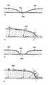
본 발명에서는, 유기 수지막으로서 감광성 아크릴 수지를 사용하고 있다. 이 감광성 유기 수지로서는, 광, 전자, 또는 이온 등의 에너지 빔에 노출된 부분이 제거되는 포지티브형 감광성 유기 수지와, 노출된 부분이 남게 되는 네거티브형 감광성 유기 수지를 들 수 있다. 도 1(A)∼도 1(D)는, 포지티브형 아크릴 수지의 개구부와 네거티브형 아크릴 수지의 개구부의 단면도를 나타낸다.In this invention, the photosensitive acrylic resin is used as an organic resin film. Examples of the photosensitive organic resin include positive photosensitive organic resins from which portions exposed to energy beams such as light, electrons, and ions are removed, and negative photosensitive organic resins from which exposed portions remain. 1 (A) to 1 (D) show cross-sectional views of an opening of a positive acrylic resin and an opening of a negative acrylic resin.
포지티브형 아크릴 수지의 경우에는, 도 1(A)에 도시된 바와 같이, 제1 무기 절연막(7000)이 형성된 후, 포지티브형 아크릴 유기 수지막을 형성하고, 그 유기 수지막의 개구될 부분을 노광시킨다. 그 후, 노광된 부분을 현상에 의해 제거하여 제1 무기 절연막(7000)을 노출시킨다. 그 다음, 개구부가 형성된 포지티브형 유기 수지막(7001)과 제1 무기 절연막(7000)의 노출된 부분을 덮도록 제2 무기 절연막(7002)을 형성한다.In the case of the positive acrylic resin, as shown in Fig. 1A, after the first inorganic insulating
도 1(B)는 개구된 포지티브형 유기 수지막(7001)의 단면의 확대도를 나타낸다. 도 1(B)에 도시된 바와 같이, 개구부의 단면은 곡선을 이루고 있고, 포지티브형 유기 수지막(7001)의 표면상의 각 부분에서의 법선의, 기판 방향(수평 방향)에 대한 기울기는 개구부로부터 멀어질수록 작게 되어 있다. 다시 말하면, 각 접점(R1, R2, R3)에서의 곡률 반경은 개구부로부터 멀어질수록 연속적으로 증가하고, 포물선을 이룬다. 그래서, 모든 접점(R1, R2, R3)의 곡률 중심은 포지티브형 유기 수지막(7001)측(기판측)에 존재한다.1B shows an enlarged view of a cross section of the opened positive
포지티브형 아크릴 수지를 사용한 경우, 포지티브형 유기 수지막(7001)이 끊어져 있는 부분의 접점에서의 법선의, 기판에 대한 각도(θ)는 30°이상 65°이하로 할 수 있다.When positive type acrylic resin is used, the angle (theta) with respect to the board | substrate of the normal in the contact part of the part where the positive type
이와 같이 하여, 포지티브형 유기 수지막의 경우에는, 개구부에서의 유기 수지막의 표면상의 곡률 중심 모두가 기판측에 존재하고, 에칭 불량으로 인해 막의 일부가, 개구되어야 할 부분에 남는 일이 적게 된다. 이에 따라, 콘택트 불량이 발생하는 것이 적게 되어, 수율의 증대로 이어진다.In this manner, in the case of the positive organic resin film, all of the centers of curvature on the surface of the organic resin film in the opening portion are present on the substrate side, and a part of the film is less likely to remain in the portion to be opened due to poor etching. As a result, contact failures are less likely to occur, leading to an increase in yield.
네거티브형 아크릴 수지의 경우에는, 도 1(C)에 도시된 바와 같이, 제1 무기 절연막(7005)이 형성된 후, 네거티브형 아크릴 유기 수지막을 형성하고, 그 유기 수지막의 개구될 부분 이외의 부분을 노광시킨다. 그 후, 노광되지 않은 부분을 현상에 의해 제거하여 제1 무기 절연막(7005)을 노출시킨다. 그 다음, 개구부가 형성된 네거티브형 유기 수지막(7006)과 제1 무기 절연막(7005)의 노출된 부분을 덮도록 제2 무기 절연막(7007)을 형성한다.In the case of the negative acrylic resin, as shown in Fig. 1C, after the first inorganic insulating
도 1(D)는 개구된 네거티브형 유기 수지막(7006)의 단면의 확대도를 나타낸다. 도 1(D)에 도시된 바와 같이, 개부부의 단면은 곡선을 이루고 있고, 네거티브형 유기 수지막(7006)의 표면상의 각 부분에서의 법선의, 기판 방향(수평 방향)에 대한 기울기는 개구부의 접점(R0)으로부터 개구부의 외측 쪽으로 멀어질수록 작게 되어 있다. 다시 말하면, 각 접점(R1, R2, R3)(제2 지점 및 제4 지점)에서의 곡률 반경은 접점(R0)으로부터 개구부의 외측 쪽으로 멀어질수록 연속적으로 증가한다. 예를 들어, 포지티브형 감광성 아크릴 수지의 경우, 노광 조건에 따라 달라지기는 하지만, 최소 곡률 반경은 그의 단부에서 3∼30 ㎛ 정도로 된다. 법선의 기울기는 접점(R0)으로부터 개구부의 중심 쪽으로 갈 수록 감소하고, 곡률 반경이 연속적으로 증가한다. 그래서, 접점(R0)으로부터 개구부의 외측에 위치하는 모든 접점(R1, R2, R3)(제2 지점 및 제4 지점)의 곡률 중심은 네거티브형 유기 수지막(7006)측(기판측)에 존재한다. 접점(R0)으로부터 개구부의 중심측에 위치하는 접점(R-1)(제1 지점 및 제3 지점)의 곡률 중심은 네거티브형 유기 수지막(7006)의 반대측(기판의 반대측)에 존재한다.1D shows an enlarged view of a cross section of the opened negative
상기한 바와 같이, 네거티브형 유기 수지막의 경우에는, 개구부에서의 유기 수지막의 표면상의 곡률 중심이 접점(R0)으로부터 중심 쪽으로 기판의 반대측에 존재한다. 접점(R0)으로부터 네거티브형 유기 수지막(7006)이 끊어져 있는 부분까지의 거리가 길 수록 개구부의 면적이 작게 되고, 콘택트 불량이 발생하기 쉽게 된다. 이 거리는 에칭 조건 또는 개구 전의 유기 수지막의 두께에 따라 변한다. 또한, 도 1(A)∼도 1(D)는 아크릴 수지의 경우를 예로 들어 나타내고 있으나, 아크릴 유기 수지막 이외의 유기 수지막을 사용하는 경우에는, 접점(R0)으로부터 유기 수지막이 끊어져 있는 부분까지의 거리는 수지의 조성에 따라서도 변한다. 그리하여, 네거티브형 감광성 유기 수지를 사용하여, 도 1(C) 및 도 1(D)에 나타낸 단면 형상을 형성하는 경우라도, 접점(R0)으로부터 네거티브형 유기 수지막(7006)이 끊어져 있는 부분까지의 거리를, 개구부의 면적을 충분히 확보할 수 있게 하는 정도까지 감소시킬 수만 있다면, 네거티브형 감광성 유기 수지를 사용하는 것도 가능하다.As described above, in the case of the negative organic resin film, the center of curvature on the surface of the organic resin film in the opening portion is on the opposite side of the substrate from the contact point R0 toward the center. The longer the distance from the contact R0 to the portion where the negative
그러나, 층간절연막의 일부로서 사용할 수지로서는, 도 1(A) 및 도 (1B)에 나타낸 단면 형상을 형성할 수 있는 유기 수지가 도 1(C) 및 도 1(D)에 나타낸 단면 형상을 형성하는 유기 수지보다 여전히 바람직하다. 그러나, 모든 포지티브형 감광성 유기 수지가 도 1(A) 및 도 1(B)에 나타낸 단면 형상을 항상 형성할 수 있는 것은 아니다. 포지티브형 아크릴이 도 1(A) 및 도 1(B)에 나타낸 단면 형상을 형성할 수 있지만, 포지티브형 폴리이미드는 그러한 단면 형상을 형성할 수 없다.However, as the resin to be used as part of the interlayer insulating film, an organic resin capable of forming the cross-sectional shape shown in Figs. 1A and 1B forms the cross-sectional shape shown in Figs. 1C and 1D. It is still more preferable than organic resin. However, not all positive photosensitive organic resins can always form the cross-sectional shape shown in FIG. 1 (A) and FIG. 1 (B). Positive acrylics can form the cross-sectional shapes shown in FIGS. 1A and 1B, but positive polyimides cannot form such cross-sectional shapes.
또한, 비감광성 유기 수지를 사용하는 경우에는, 층간절연막에 개구를 형성하기 위해 일반적인 건식 에칭을 사용한다. 이 건식 에칭은 활성 라디컬 또는 반응성 가스의 플라즈마를 사용하는 에칭법이다. 층간절연막은 게이트 절연막의 두께의 10배 정도의 두께를 가지기 때문에, 개구를 형성하는 목적의 건식 에칭은 시간이 걸린다. TFT가 형성되어 있는 기판이 장시간 플라즈마에 노출되면, 게이트 절연막에 정공이 트랩되는 소위 차징 데미지(charging damage)로 인해 TFT의 스레시홀드값이 정(正)의 값 측으로 변동하기 쉽게 된다. 그리하여, 본 발명에서와 같이 감광성 유기 수지를 사용하여 습식 에칭으로 개구를 형성함으로써, 건식 에칭에서 소요되는 시간을 대폭 감소시킬 수 있고, TFT의 스레시홀드값의 변동을 억제할 수 있다.In addition, when using a non-photosensitive organic resin, general dry etching is used in order to form an opening in an interlayer insulation film. This dry etching is an etching method using a plasma of an active radical or a reactive gas. Since the interlayer insulating film has a thickness about ten times the thickness of the gate insulating film, the dry etching for the purpose of forming the opening takes time. When the substrate on which the TFT is formed is exposed to plasma for a long time, the threshold value of the TFT tends to fluctuate toward the positive value due to so-called charging damage in which holes are trapped in the gate insulating film. Thus, by forming the opening by wet etching using the photosensitive organic resin as in the present invention, the time required for the dry etching can be greatly reduced, and variations in the threshold value of the TFT can be suppressed.
또한, 본 발명에서는, TFT의 게이트 전극과, 반도체 표시장치의 구동회로에 사용되는 용량의 한쪽 전극을 동시에 형성하고, TFT에 전기적으로 접속되는 배선과 용량의 다른 쪽 전극을 동시에 형성한다. 그 다음, 유기 수지막의 개구부에서, 2층의 무기 절연막들을 2개의 전극 사이에서 이들 전극과 서로 중첩시켜, 보유 용량을 형성한다.In the present invention, the gate electrode of the TFT and one electrode of the capacitor used in the driving circuit of the semiconductor display device are simultaneously formed, and the wiring electrically connected to the TFT and the other electrode of the capacitor are simultaneously formed. Next, in the opening portion of the organic resin film, two layers of inorganic insulating films are overlapped with each other between the two electrodes to form a storage capacitor.
반도체 표시장치는 그의 구동회로가 유기 기판상에 형성되기 때문에, FPC의 핀의 개수를 감소시킬 수 있고, 물리적 충격 저항을 증가시킬 수 있고, 반도체 표시장치 자체의 크기를 억제할 수 있다. 또한, FPC의 접속 불량으로 인한 수율 감소를 억제할 수 있다.Since the semiconductor display device is formed on the organic substrate, the number of the pins of the FPC can be reduced, the physical impact resistance can be increased, and the size of the semiconductor display device itself can be suppressed. In addition, it is possible to suppress a decrease in yield due to poor connection of the FPC.
구동회로의 대표적인 예로서는, 화소부에 제공되어 있는 복수의 화소 중 하나 또는 수개의 화소를 차례로 선택하는 주사선 구동회로와, 선택된 화소(들)에 화상 정보를 가지는 신호(비디오 신호)를 입력하는 신호선 구동회로를 들 수 있다. 이들 구동회로는 모두 본 발명을 이용하여 형성될 수 있다. 특히, 본 발명을 이용하여 형성되는 용량은, 예를 들어, 신호선 구동회로의 용량 분할형 D/A 변환회로에 포함되는 용량으로서 사용하는 것이 가능하다.As a representative example of the driving circuit, a scanning line driving circuit for sequentially selecting one or several pixels among the plurality of pixels provided in the pixel portion, and a signal line driving circuit for inputting a signal (video signal) having image information to the selected pixel (s) For example. All of these drive circuits can be formed using the present invention. In particular, the capacitance formed using the present invention can be used, for example, as a capacitance included in the capacitance division type D / A conversion circuit of the signal line driver circuit.
또한, 규소 기판상에 형성되었던 콘트롤러 또는 CPU 등의, 반도체 표시장치에 사용되는 다른 반도체장치를 본 발명을 이용하여 유리 기판 상에 일체로 형성하는 것이 가능하다. 특히, 본 발명의 용량을 사용하여 제조되는 용량은 승압 회로, DRAM(Dynamic Random Access Memory), 아날로그 래치, 용량 분할형 D/A 변환회로, 정전기 대처용 보호회로 등의 모든 회로에 포함되는 용량으로서 사용될 수 있다.In addition, it is possible to integrally form another semiconductor device used for a semiconductor display device such as a controller or a CPU formed on a silicon substrate on a glass substrate by using the present invention. In particular, the capacity manufactured using the capacity of the present invention is a capacity included in all circuits such as a boost circuit, a dynamic random access memory (DRAM), an analog latch, a capacity division type D / A conversion circuit, and an antistatic protection circuit. Can be used.
반도체 표시장치에서 사용되는 콘트롤러 및 CPU 등의 다른 회로를 유리 기판상에 일체로 형성함으로써, FPC의 핀의 개수를 더욱 감소시킬 수 있고, 물리적 충격 저항을 증가시킬 수 있고, 반도체 표시장치 자체의 크기를 억제할 수 있다. 또한, FPC의 접속 불량으로 인한 수율 감소를 더욱 억제할 수 있다.By integrally forming other circuits such as a controller and a CPU used in the semiconductor display on the glass substrate, the number of pins of the FPC can be further reduced, the physical impact resistance can be increased, and the size of the semiconductor display itself Can be suppressed. In addition, it is possible to further suppress a decrease in yield due to poor connection of the FPC.
도 2는 포지티브형 감광성 폴리이미드를 사용하는 경우의 개구부의 단면의 확대도를 나타낸다. 도 2에 도시된 바와 같이, 포지티브형 아크릴을 사용하는 경우와 동일한 방식으로 제1 무기 절연막(7010)을 형성한 후 포지티브형 폴리이미드막을 형성한다. 그 다음, 개구시킬 부분을 노광한 후 그 부분을 현상하여 개구부를 형성함으로써 제1 무기 절연막(7010)을 노출시킨다. 그 다음, 개구부가 형성되어 있는 포지티브형 폴리이미드막(7011)과, 제1 무기 절연막(7010)의 노출된 부분을 덮도록 제2 무기 절연막(7012)을 형성한다.2 shows an enlarged view of a cross section of an opening when using a positive photosensitive polyimide. As shown in FIG. 2, the first inorganic insulating
개구부가 형성되어 있는 포지티브형 폴리이미드막(7011)의 단부가 그 개구부에서 충분히 둥글게 되어 있지 않기 때문에, 제2 무기 절연막(7012)상에 배선을 형성하는 경우, 단부에서 배선의 막 두께가 감소되어 배선 저항이 증가하게 된다. 또한, 기상 성장법에 의해 제2 무기 절연막(7012)을 형성하는 경우에는, 개구부에서의 포지티브형 폴리이미드막(7011)의 단부가 충분히 둥글게 되어 있지 않기 때문에, 제2 무기 절연막(7012)의 단부(7013)에서서의 두께가 다른 부분에서의 두께보다 두껍게 형성될 수 있다. 이는 박막을 구성하는 재료의 분자가 피형성면에 부착할 때 재료 분자가 안정한 자리를 찾아 표면상에서 이동하지만, 콘택트 홀의 상단부와 같이 예각을 가지는 형상(돌출부가 되는 형상)의 부분에 모이게 되는 경향이 있기 때문이다. 이러한 경향은 특히 증착법에서 현저하다. 제2 무기 절연막(7012)이 단부(7013)에서 부분적으로 두껍게 형성되면, 배선의 막 두께가 특히 단부에서 감소하여 배선 저항을 증가시킨다.Since the end portion of the positive polyimide film 7071 having the opening formed therein is not sufficiently rounded at the opening, when the wiring is formed on the second inorganic insulating film 7092, the film thickness of the wiring at the end is reduced. The wiring resistance is increased. In the case of forming the second inorganic insulating
따라서, 본 발명의 층간절연막의 일부로서, 도 2에 도시된 바와 같이 개구부의 단부에서 곡선이 아닌 단면 형상을 형성하는 포지티브형 감광성 폴리이미드 또는 다른 유기 수지를 사용하는 것은 바람직하지 않다.Therefore, as part of the interlayer insulating film of the present invention, it is not preferable to use positive photosensitive polyimide or other organic resin which forms a cross-sectional shape rather than a curve at the end of the opening as shown in FIG.
다음에, 무기 절연막을 개구시키기 위해 에칭에 의해 콘택트 홀을 형성할 때의 콘택트 홀 부근의 단면에 대하여 설명한다. 도 1(A)에 도시된 상태까지 막을 형성한 후, 도 3(A)에 도시된 바와 같이, 레지스트 마스크(7021)를 형성하고, 제1 무기 절연막(7000), 제2 무기 절연막(7002), 및 제1 무기 절연막(7000)과 반도체막 사이에 형성된 게이트 절연막(7022)에 대해 건식 에칭을 실시하여, 콘택트 홀(7023)을 형성한다.Next, the cross section of the vicinity of a contact hole at the time of forming a contact hole by etching in order to open an inorganic insulating film is demonstrated. After the film is formed to the state shown in FIG. 1A, as shown in FIG. 3A, a resist
도 3(B)는 기판의 상면에서 본 콘택트 홀 부근의 상태를 나타낸다. 도면을 보기 쉽게 하기 위해, 레지스트 마스크(7021)를 게거한 후의 상태를 나타낸다. 도 3(B)의 선 A-A'에 따른 단면도가 도 3(A)에 상당한다.3B shows a state near the contact hole seen from the upper surface of the substrate. In order to make drawing easy to see, the state after removing the resist
콘택트 홀(7023)이 포지티브형 유기 수지막(7001)에 형성된 개구부(7024)의 내측에 형성된다. 그 다음, 도 3(C)에 도시된 바와 같이, 콘택트 홀(7023)을 덮도록 제2 무기 절연막(7002)상에 도전막(7025)을 형성한 다음, 도전막(7025)을 패터닝하여 배선을 형성한다.The contact hole 7203 is formed inside the
도 4(A)∼도 4(D)는 포지티브형 유기 수지막(7001)의 개구부(7024)와 콘택트 홀(7023)과의 위치 관계를 나타낸다. 도 4(A)는 콘택트 홀(7023) 부근의 상면도를 나타내고, 도 4(B)는 도 4(A)의 선 A-A'에 따른 단면도를 나타낸다.4A to 4D show the positional relationship between the
도전막(7025)을 패터닝하여 얻어진 배선(7026)이 개구부(7024)의 대체로 중심에 형성된 콘택트 홀(7023)을 통해 게이트 절연막(7022)의 아래에 형성된 반도체막(7300)과 접속되어 있다.The
이와 같이 하여, 콘택트 홀(7023)은 항상 개구부(7024)내에 위치되도록 형성되고, 포지티브형 유기 수지막(7001)이 콘택트 홀(7023)의 형성으로 인해 콘택트 홀(7023)에서 노출되지 않도록 한다.In this way, the contact hole 7203 is formed so as to be always located in the
도 4(A) 및 도 4(B)에서는 콘택트 홀(7023)이 개구부(7024)의 대체로 중심에 위치되도록 레이아웃되어 있으나, 본 발명은 이러한 구성에 한정되지 않는다. 콘택트 홀(7023)은 개구부(7024)내에 위치하기만 하면 되고, 일 방향으로 치우쳐 있어도 좋다.4 (A) and 4 (B), the contact hole 7203 is laid out so as to be positioned substantially in the center of the
도 4(C)는 콘택트 홀(7023)이 개구부(7024)내에서 일 방향으로 치우쳐 있는 경우의 콘택트 홀(7023) 부근의 상면도를 나타낸다. 도 4(D)는 도 4(C)의 선 B-B'에 따른 단면도를 나타낸다.FIG. 4C shows a top view of the vicinity of the contact hole 7203 when the contact hole 7203 is oriented in one direction in the
도전막(7025)을 패터닝하여 얻어진 배선(7026)이, 개구부(7024)내에서 도면의 상측 방향으로 치우쳐 있는 콘택트 홀(7023)을 통해 게이트 절연막(7022) 아래에 형성된 반도체막(도시되지 않음)과 접속되어 있다.The
다음에, 본 발명의 반도체 표시장치의 TFT 및 용량의 구조에 대하여 도 5(A) 및 도 5(B)를 참조하여 설명한다.Next, the structure of the TFT and the capacitor of the semiconductor display device of the present invention will be described with reference to FIGS. 5A and 5B.
도 5(A)에서, 절연 표면(8000)상에 TFT(8001)가 형성되어 있다. TFT(8001)는 탑 게이트형이고, 반도체막(8002), 그 반도체막(8002)과 접하여 있는 게이트 절연막(8003), 및 그 게이트 절연막(8003)과 접하여 있는 게이트 전극(8004)을 가지고 있다. 반도체막(8002)은 절연 표면(8000)과 접하여 있다. 반도체막(8002)은 채널 형성 영역(8005)과, 그 채널 형성 영역(8005)의 양측에 존재하는 불순물 영역(8006)을 가지고 있다.In FIG. 5A, a
한편, 게이트 절연막(8003)상에 형성된 용량용 제1 전극(8007)은 게이트 전극(8004)과 동일한 도전막으로부터 형성될 수 있다.On the other hand, the
그 다음, TFT(8001)와 용량용 제1 전극(8007)을 덮도록 제1 무기 절연막(8008)이 형성된다. 제1 무기 절연막(8008)은 질소를 함유하는 절연막이고, 후에 형성되는 유기 수지막에 비해 수분을 투과시키기 어려운 성질을 가지고 있다.Then, a first inorganic insulating
그 다음, 제1 무기 절연막(8008)상에 감광성 유기 수지를 도포한 후, 그 감광성 유기 수지를 소성하고, 개구시킬 부분을 노광 및 현상함으로써, 개구부를 가지는 유기 수지막(8009)이 형성된다. 이때, 제1 무기 절연막(8008)의 일부가 개구부에서 노출된다.Then, after the photosensitive organic resin is coated on the first inorganic insulating
그 다음, 유기 수지막(8009)과, 개구부에서 노출된 제1 무기 절연막(8008)의 일부를 덮도록, 제2 무기 절연막(8010)이 형성된다. 제1 무기 절연막(8008)과 마찬가지로, 제2 무기 절연막(8010)도 질소를 함유하는 절연막이고, 유기 수지막에 비해 수분을 투과시키기 어려운 성질을 가지고 있다.Next, the second inorganic insulating
제1 무기 절연막(8008)과 제2 무기 절연막(8010)이 용량의 유전체로서 사용되기 때문에, 이들 막이 너무 두꺼우면, 용량의 용량값이 감소하게 되고, 성막에 소요되는 처리 시간이 억제될 수 없다. 이와는 반대로, 상기 막들이 너무 얇으면, 수분 투과를 방지하는 효과가 약화된다. 제1 무기 절연막(8008)과 제2 무기 절연막(8010)은 10 nm∼200 nm 정도의 막 두께를 가지는 것이 바람직하고, 2개 막의 총 막 두께는 20 nm∼400 nm 정도가 바람직하다.Since the first inorganic insulating
그 다음, 유기 수지막(8009)의 개구부에서, 반도체막의 일부를 노출시키도록 게이트 절연막(8003), 제1 무기 절연막(8008), 및 제2 무기 절연막(8010)에 대해 건식 에칭을 실시하여 콘택트 홀을 형성한다. 이 경우, 반도체막(8002)은 에칭 스토퍼로서의 기능을 가진다.Next, in the opening of the
이때, 용량용 제1 전극(8007)상에 존재하는 제1 무기 절연막(8008)과 제2 무기 절연막(8010)은 에칭되지 않도록 레지스트 마스크로 덮여 있다.At this time, the first inorganic insulating
그 다음, 레지스트 마스크를 현상액으로 제거한다. 일반적으로, 현상액으로서는, 알칼리성 수용액이 사용되고, 이것은 다량의 수분을 함유하고 있다. 본 발명에서는, 유기 수지막(8009)이 제1 무기 절연막(8008)과 제2 무기 절연막(8010)으로 덮여 있기 때문에, 유기 수지막(8009)이 현상액에 직접 노출되는 일은 없다. 그리하여, 현상액의 수분이 유기 수지막(8009)에 침입하여 습윤시키는 일이 적게 된다. 따라서, 레지스트 마스크를 현상액으로 제거한 후, 수분을 제거할 목적으로 행하는 가열처리의 시간이 감소될 수 있다.Then, the resist mask is removed with a developer. Generally, as a developing solution, an alkaline aqueous solution is used, which contains a large amount of water. In the present invention, since the
그 다음, 도전막이 콘택트 홀을 덮도록 제2 무기 절연막(8010)상에 형성된 다음, 이 도전막을 에칭하여, 반도체막(8002)에 접속되는 배선(8011)과 용량용 제2 전극(8012)을 형성한다. 용량용 제2 전극(8012)은 제1 무기 절연막(8008) 및 제2 무기 절연막(8010)을 사이에 두고 용량용 제1 전극(8007)과 겹쳐 있다. 이와 같이 하여, 용량용 제2 전극(8012), 제1 무기 절연막(8008), 제2 무기 절연막(8010), 및 용량용 제1 전극(8007)에 의해 보유 용량(8013)이 형성되어 있다.Next, a conductive film is formed on the second inorganic insulating
본 발명은 이 보유 용량(8013)을 반도체 표시장치의 구동회로, CPU, 콘트롤러, 또는 다른 회로에 포함되는 용량으로서 사용하는 것에 특징을 가지고 있다. TFT(8001)는 탑 게이트형일 수도 있고 보텀 게이트형일 수도 있다.The present invention is characterized by using this
도 5(A)의 보유 용량 외에, 반도체막과 용량용 제1 전극(8007) 사이에 보유 용량이 추가로 형성될 수도 있다. 도 21은, 게이트 절연막(8052)을 사이에 두고 용량용 제1 전극(8051)과 용량용 반도체막(8050)을 서로 중첩시켜 제1 보유 용량(8053)을 형성한 예를 나타낸다. 또한, 도 5(A)와 마찬가지로, 제1 무기 절연막(8055) 및 제2 무기 절연막(8056)을 사이에 두고 용량용 제1 전극(8051)과 용량용 제2 전극(8054)을 서로 중첩시켜 제2 보유 용량(8057)을 형성한다. 이와 같이 하여, 용량들을 상하로 형성함으로써, 동일 면적에서의 용량값을 증대시킬 수 있다.In addition to the storage capacitor shown in Fig. 5A, a storage capacitor may be further formed between the semiconductor film and the
도 5(B)는 TFT가 보텀 게이트형인 경우의 본 발명의 반도체 표시장치의 구조를 나타낸다.Fig. 5B shows the structure of the semiconductor display device of the present invention when the TFT is a bottom gate type.
도 5(B)에서, 절연 표면(8100)상에 TFT(8101)가 형성되어 있다. TFT(8101)는 보텀 게이트형이고, 반도체막(8102), 그 반도체막(8102)과 접하여 있는 게이트 절연막(제1 절연막)(8103), 및 그 게이트 절연막(8103)과 접하여 있는 게이트 전극(8104)을 가지고 있다. 게이트 전극(8104)은 절연 표면(8100)과 접하여 있다. 반도체막(8102)은 채널 형성 영역(8105)과, 그 채널 형성 영역(8105)의 양측에 존재하는 불순물 영역(8106)을 가지고 있다. 부호 8115는 반도체막에 불순물을 첨가할 때 마스크로서 사용되는 절연막으로서, 본 명세서에서는 채널 보호막이라 칭한다.In FIG. 5B, a
한편, 절연 표면(8100)상에 형성된 용량용 제1 전극(8107)은 게이트 전극(8104)과 동일한 도전막으로부터 형성될 수 있다.Meanwhile, the first electrode for capacitance 807 formed on the insulating
그 다음, TFT(8001)와 용량용 제1 전극(8107)을 덮도록 제1 무기 절연막(제2 절연막)(8108)이 형성된다. 그 다음, 제1 무기 절연막(8108)상에 감광성 유기 수지를 도포한 후, 그 감광성 유기 수지를 소성하고, 개구시킬 부분을 노광 및 현상함으로써, 개구부(제2 개구부 및 제3 개구부)를 가지는 유기 수지막(제3 절연막)(8109)이 형성된다. 이때, 제1 무기 절연막(제2 절연막)(8108)의 일부가 개구부(제2 개구부 및 제3 개구부)에서 노출된다.Next, a first inorganic insulating film (second insulating film) 8108 is formed to cover the
그 다음, 유기 수지막(제3 절연막)(8109)과, 개구부(제2 개구부 및 제3 개구부)에서 노출된 제1 무기 절연막(제1 절연막)(8108)의 일부를 덮도록, 제2 무기 절연막(제4 절연막)(8110)이 형성된다. 제1 무기 절연막(8108)과 마찬가지로, 제2 무기 절연막(제4 절연막)(8110)도 질소를 함유하는 절연막이고, 유기 수지막에 비해 수분을 투과시키기 어려운 성질을 가지고 있다.Next, a second inorganic layer is formed so as to cover a portion of the organic resin film (third insulating film) 8109 and the first inorganic insulating film (first insulating film) 8108 exposed through the openings (second openings and third openings). An insulating film (fourth insulating film) 8110 is formed. Similar to the first inorganic insulating
제1 무기 절연막(8108)과 제2 무기 절연막(8110)이 용량의 유전체로서 사용되기 때문에, 이들 막이 너무 두꺼우면, 용량의 용량값이 감소하게 되고, 성막에 소요되는 처리 시간이 억제될 수 없다. 이와는 반대로, 상기 막들이 너무 얇으면, 수분 투과를 방지하는 효과가 약화된다. 또한, 보텀 게이트형 TFT의 경우에는, 용량용 제1 전극(8107)과 용량용 제2 전극(8112) 사이에도 게이트 절연막(제1 절연막)(8103)이 존재하고, 유전체의 일부로서 사용된다. 따라서, 게이트 절연막(제1 절연막)(8103)의 막 두께를 고려하여 제1 무기 절연막(8108)과 제2 무기 절연막(8110)의 막 두께를 결정할 필요가 있다. 제1 무기 절연막(8108)과 제2 무기 절연막(8110)은 10 nm∼200 nm 정도의 막 두께를 가지는 것이 바람직하고, 게이트 절연막(8103)을 포함한 3개 막의 총 막 두께는 30 nm∼500 nm 정도가 바람직하다.Since the first inorganic insulating
그 다음, 유기 수지막(제2 개구부)(8109)의 개구부에서, 반도체막의 일부를 노출시키도록 게이트 절연막(8103), 제1 무기 절연막(8108), 및 제2 무기 절연막(8110)에 대해 건식 에칭을 실시하여 콘택트 홀(제1 개구부)을 형성한다. 이때, 반도체막(8102)은 에칭 스토퍼로서의 기능을 가진다. 또한, 용량용 제1 전극(8107)상에 존재하는 제1 무기 절연막(8108)과 제2 무기 절연막(8110)은 에칭되지 않도록 레지스트 마스크로 덮인다.Next, in the opening portion of the organic resin film (second opening portion) 8109, dry to the
그 다음, 레지스트 마스크를 현상액으로 제거한다. 일반적으로, 현상액으로서는, 알칼리성 수용액이 사용되고, 이것은 다량의 수분을 함유한다. 본 발명에서는, 유기 수지막(8109)이 제1 무기 절연막(8108)과 제2 무기 절연막(8110)으로 덮여 있기 때문에, 유기 수지막(8109)이 현상액에 직접 노출되는 일은 없다. 이와 같이 하여, 현상액의 수분이 유기 수지막(8109)에 침입하여 습윤시키는 일이 적게 된다. 따라서, 레지스트 마스크를 현상액으로 제거한 후, 수분을 제거할 목적으로 행하는 가열처리의 시간이 감소될 수 있다.Then, the resist mask is removed with a developer. Generally, as a developing solution, an alkaline aqueous solution is used, which contains a large amount of water. In the present invention, since the
그 다음, 도전막이 콘택트 홀(제1 개구부 및 제2 개구부)을 덮도록 제2 무기 절연막(8110)상에 형성된 다음, 이 도전막을 에칭하여, 반도체막(8102)에 접속되는 배선(8111)과 용량용 제2 전극(8112)을 형성한다. 용량용 제2 전극(8112)은 제1 무기 절연막(8108) 및 제2 무기 절연막(8110)을 사이에 두고 용량용 제1 전극(8107)과 겹쳐 있다. 이와 같이 하여, 용량용 제2 전극(8112), 제1 무기 절연막(8108), 제2 무기 절연막(8110), 및 용량용 제1 전극(8107)에 의해 보유 용량(8113)이 형성되어 있다.Then, a conductive film is formed on the second inorganic insulating
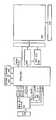
다음에, 본 발명을 이용하여 제조된 반도체 표시장치의 구동회로의 구성의 일 예를 설명한다.Next, an example of the configuration of a drive circuit of a semiconductor display device manufactured using the present invention will be described.
도 6(A)는 본 발명의 반도체 표시장치의 블록도를 나타낸다. 부호 115는 신호선 구동회로이고, 116은 주사선 구동회로이고, 120은 화소부이다. 신호선 구동회로(115)는 시프트 레지스터 회로(115_1), 레벨 시프트 회로(115_2), 및 샘플링 회로(115_3)를 가지고 있다. 도 6(A)에서는 레벨 시프트 회로(115_2)가 시프트 레지스터 회로(115_1)와 샘플링 회로(115_3) 사이에 제공되어 있으나, 레벨 시프트 회로(115_2)가 시프트 레지스터 회로(115_1)에 포함되어도 좋다.Fig. 6A shows a block diagram of the semiconductor display device of the present invention.
또한, 부호 121은 공급된 전원 전압으로부터 구동회로에 공급되는 다양한 레벨의 전원 전압을 생성할 수 있는 승압 회로를 나타낸다.
시프트 레지스터 회로(115_1)에 클록 신호(CLK)와 스타트 펄스 신호(SP)가 공급되면, 시프트 레지스터 회로(115_1)는 비디오 신호를 샘플링하기 위한 타이밍을 제어하기 위한 타이밍 신호를 생성한다.When the clock signal CLK and the start pulse signal SP are supplied to the shift register circuit 115_1, the shift register circuit 115_1 generates a timing signal for controlling timing for sampling the video signal.
이와 같이 하여 생성된 타이밍 신호는 레벨 시프트 회로(115_2)에 공급된다. 한편, 승압 회로(121)에서 생성된 전원 전압은 레벨 시프트 회로(115_2)에 공급되고, 레벨 시프트 회로(115_2)는 공급된 전원 전압을 사용하여 타이밍 신호의 전압의 진폭을 증폭시킨다.The timing signal generated in this way is supplied to the level shift circuit 115_2. On the other hand, the power supply voltage generated by the
레벨 시프트 회로(115_2)에서 증폭된 타이밍 신호는 샘플링 회로(115_3)에 입력된다. 그리고, 샘플링 회로(115_3)에 입력된 비디오 신호는 샘플링 회로(115_3)에 입력된 타이밍 신호에 동기하여 샘플링되고, 신호선을 통해 화소부(120)에 입력된다.The timing signal amplified by the level shift circuit 115_2 is input to the sampling circuit 115_3. The video signal input to the sampling circuit 115_3 is sampled in synchronization with the timing signal input to the sampling circuit 115_3 and input to the
도 6(B)는 승압 회로(121)의 회로도의 일 예를 나타낸다. 도 6(B)에 도시된 승압 회로는 2개의 n채널형 TFT(122, 123)와 2개의 보유 용량(124, 125)을 가지고 있다. 여기에 도시된 승압 회로는 단지 예일 뿐이고, 본 발명이 이 승압회로에 한정되는 것은 아니다.6B shows an example of a circuit diagram of the
n채널형 TFT(122)의 게이트와 드레인 모두에 전원 전압(Vdd)이 공급된다. 여기서, Vdd > Gnd 이다. 또한, n채널형 TFT(123)의 게이트와 드레인 모두가 n채널형 TFT(122)의 소스에 접속되어 있다. 용량(124)에 포함된 2개의 용량용 전극들 중 한쪽 전극이 n채널형 TFT(122)의 소스에 접속되어 있고, 상기 2개의 전극들 중 다른쪽 전극에는 클록 신호(CLK)가 공급된다. 또한, 용량(125)에 포함된 2개의 용량용 전극들 중 한쪽 전극이 n채널형 TFT(123)의 소스에 접속되고, 상기 2개의 전극들 중 다른쪽 전극이 Gnd에 접속되어 있다. n채널형 TFT(123)의 소스의 전압이 레벨 시프트 회로(115_2)에 전원 전압으로서 공급된다.The power supply voltage Vdd is supplied to both the gate and the drain of the n-
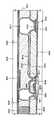
도 7(A)는 도 6(B)에 도시된 승압 회로의 상면도를 나타낸다. 도 7(A)의 선 A-A'에 따른 단면도가 도 7(B)에 상당한다.FIG. 7A shows a top view of the boosting circuit shown in FIG. 6B. A cross-sectional view along the line A-A 'in FIG. 7A corresponds to FIG. 7B.
n채널형 TFT(123)는 반도체막(124), 게이트 절연막(125), 및 게이트 전극(126)을 가지고 있다. 또한, n채널형 TFT(123)는 제1 무기 절연막(128)으로 덮여 있다. 또한, 개구부를 가진 유기 수지막(129)이 제1 무기 절연막(128)상에 형성되어 있고, 그 유기 수지막(129)을 덮도록 제2 무기 절연막(130)이 형성되어 있다.The n-
배선(127)이 게이트 절연막(125), 제1 무기 절연막(128), 및 제2 무기 절연막(130)에 형성된 콘택트 홀을 통해 유기 수지막(129)의 개구부에서 게이트 전극(126) 및 반도체막(124)에 접속되어 있다. 또한, 배선(131)이 게이트 절연막(125), 제1 무기 절연막(128), 및 제2 무기 절연막(130)에 형성된 콘택트 홀을 통해 유기 수지막(129)의 개구부에서 반도체막(124)에 접속되어 있다.The
또한, 용량용 제1 전극(133)이 유기 수지막(129)의 개구부에서 제1 무기 절연막(128) 및 제2 무기 절연막(130)을 사이에 두고, 배선(131)의 일부인 용량용 제2 전극과 중첩됨으로써, 보유 용량(134)이 형성되어 있다.In addition, the second electrode for capacitance, which is a part of the
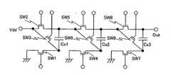
본 발명의 반도체 표시장치에 포함되는 승압 회로는 상기한 구성에 한정되는 것은 아니다. 도 23은 도 6(B)에 도시된 승압 회로와는 다른 구성을 가지는 승압 회로를 나타낸다. 도 23에 도시된 승압 회로에서는, 3개의 TFT가 하나의 용량에 대응하고, 용량의 개수와 TFT의 개수는 하나의 용량과 그 용량에 대응하는 3개의 TFT를 하나의 단위로 하여 소망의 전압의 값에 맞추어 증가될 수 있다. 도 23에서는, 용량(Cs1, Cs2, Cs3)에 각각 대응하는 스위칭 소자로서 TFT(SW1∼SW9)가 제공되어 있다.The booster circuit included in the semiconductor display device of the present invention is not limited to the above configuration. FIG. 23 shows a boosting circuit having a configuration different from that of the boosting circuit shown in FIG. 6B. In the boosting circuit shown in Fig. 23, three TFTs correspond to one capacitance, and the number of capacitances and the number of TFTs are one of the capacitance and three TFTs corresponding to the capacitance as one unit, and It can be increased to match the value. In Fig. 23, TFTs SW1 to SW9 are provided as switching elements corresponding to the capacitors Cs1, Cs2, and Cs3, respectively.
용량(Cs1, Cs2, Cs3)의 한쪽 전극(제1 전극)은 각각 SW1, SW4, SW7을 통해 접지에 접속되어 있다. 또한, 용량(Cs1, Cs2, Cs3)의 다른쪽 전극(제2 전극)은 각각 SW2와 SW3, SW5와 SW6, SW8과 SW9를 통해 제1 전극들에 접속되어 있다. 또한, SW2와 SW3의 노드(node)에는 Vdd(Vdd > 접지)가 주어진다. SW5와 SW6의 노드는 용량(Cs1)의 제1 전극에 접속되어 있다. 또한, SW8과 SW9의 노드는 용량(Cs2)의 제1 전극이 접속되어 있다. 용량(Cs3)의 제1 전극의 전압은 후단측의 회로에 인가된다.One electrode (first electrode) of the capacitors Cs1, Cs2, and Cs3 is connected to the ground via SW1, SW4, and SW7, respectively. In addition, the other electrode (second electrode) of the capacitors Cs1, Cs2, and Cs3 is connected to the first electrodes via SW2 and SW3, SW5 and SW6, and SW8 and SW9, respectively. In addition, nodes of SW2 and SW3 are given Vdd (Vdd> ground). The nodes of SW5 and SW6 are connected to the first electrode of the capacitor Cs1. The nodes of SW8 and SW9 are connected to the first electrode of the capacitor Cs2. The voltage of the first electrode of the capacitor Cs3 is applied to the circuit on the rear end side.
본 실시형태에서는, 승압 회로의 보유 용량을 예로 들어 설명하였으나, 본 발명을 이용하여 제조되는 보유 용량은 이것에 한정되지 않고, 반도체 표시장치의 다른 회로에도 사용될 수 있다. 또한, 본 실시형태에서 설명한 바와 같은 보유 용량을 사용한 반도체 회로는 화소부가 형성된 기판과는 다른 기판상에 형성되어도 좋다.In the present embodiment, the storage capacitor of the boost circuit has been described as an example, but the storage capacitor manufactured by using the present invention is not limited to this, and may be used in other circuits of the semiconductor display device. The semiconductor circuit using the storage capacitor as described in the present embodiment may be formed on a substrate different from the substrate on which the pixel portion is formed.
이하, 본 발명의 실시예를 설명한다.Hereinafter, embodiments of the present invention will be described.
[실시예 1]Example 1
본 실시예에서는, 본 발명의 반도체 표시장치의 하나인 발광장치의 제조방법에 대하여 설명한다. 본 실시예에서는, 화소부와, 그 화소부 주위에 제공되는 회로에 포함되는 보유 용량을 제조하는 방법에 대하여 상세히 설명한다.In this embodiment, a method of manufacturing a light emitting device which is one of the semiconductor display devices of the present invention will be described. In this embodiment, a method of manufacturing the pixel portion and the storage capacitor included in the circuit provided around the pixel portion will be described in detail.
먼저, 도 8(A)에 도시한 바와 같이, 코닝사의 #7059 유리나 #1737 유리 등으로 대표되는 바륨 붕규산 유리 또는 알루미노 붕규산 유리 등의 유리로 된 기판(5001)상에, 산화규소막, 질화규소막 또는 산화질화규소막 등의 절연막으로 된 하지막(5002)을 형성한다. 예를 들어, 플라즈마 CVD법에 의해 SiH4, NH3, 및 N2O로 형성되는 산화질화규소막(5002a)을 10∼200 nm(바람직하게는 50∼100 nm)의 두께로 형성하고, 마찬가지로, SiH4 및 N2O로 형성되는 산화질화수소화규소막(5002b)을 50∼200 nm(바람직하게는 100∼150 nm)의 두께로 적층 형성한다. 본 실시예에서는, 하지막(5002)을 2층 구조로 나타내었으나, 상기 절연막의 단층막 또는 상기 절연막을 2층 이상 적층한 구조로 형성할 수도 있다.First, as shown in FIG. 8 (A), a silicon oxide film and silicon nitride are formed on a
비정질 구조를 가지는 반도체막을 레이저 결정화법이나 공지의 열결정화법을 이용하여 결정화시켜 제조한 결정질 반도체막으로 섬 형상의 반도체층(5003, 5004)을 형성한다. 이 섬 형상의 반도체층(5003, 5004)은 25∼80 nm(바람직하게는 30∼60 nm)의 두께로 형성한다. 결정질 반도체막의 재료에 제한은 없으나, 바람직하게는 규소 또는 규소 게르마늄(SiGe)합금 등으로 형성하면 좋다.Island-
레이저 결정화법으로 결정질 반도체막을 제조하는 경우에는, 펄스 발진형 또는 연속 발광형의 엑시머 레이저나 YAG 레이저, YVO4레이저를 사용한다. 이들 레이저를 사용하는 경우에는, 레이저 발진기로부터 방사된 레이저광을 선형으로 집광하여 반도체막에 조사하는 방법을 이용하면 좋다. 결정화의 조건은 실시자가 적절히 선택하는 것이지만, 엑시머 레이저를 사용하는 경우에는, 펄스 발진 주파수를 300 Hz로 하고, 레이저 에너지 밀도를 100∼400 mJ/cm2(대표적으로는 200∼300 mJ/cm2)로 하는 것이 좋다. 또한, YAG 레이저를 사용하는 경우에는, 그의 제2 고조파를 사용하고, 펄스 발진 주파수를 30∼300 kHz로 하고, 레이저 에너지 밀도를 300∼600 mJ/cm2(대표적으로는 350∼500 mJ/cm2)로 하면 좋다. 그리고, 100∼1,000 ㎛의 폭, 예를 들어, 400 ㎛의 폭으로 선형으로 집광한 레이저광을 기판 전면에 걸쳐 조사하고, 이때의 선형 레이저광의 중첩비(오버랩비)를 50∼90%로 한다.When producing a crystalline semiconductor film by the laser crystallization method, an excimer laser, a YAG laser, or a YVO4 laser of pulse oscillation type or continuous emission type is used. When using these lasers, the method of irradiating a semiconductor film by linearly concentrating the laser beam radiated | emitted from the laser oscillator may be used. Crystallization conditions are appropriately selected by the practitioner, but when using an excimer laser, the pulse oscillation frequency is 300 Hz, and the laser energy density is 100 to 400 mJ / cm2 (typically 200 to 300 mJ / cm2). It is good to make). In the case of using a YAG laser, its second harmonic is used, the pulse oscillation frequency is set to 30 to 300 kHz, and the laser energy density is 300 to 600 mJ / cm2 (typically 350 to 500 mJ / cm).2 ) is good. Then, a laser beam condensed linearly with a width of 100 to 1,000 mu m, for example, 400 mu m is irradiated over the entire surface of the substrate, and the overlap ratio (overlap ratio) of the linear laser beam at this time is set to 50 to 90%. .
반도체막에는 규소뿐만 아니라 규소 게르마늄도 사용할 수 있다. 규소 게르마늄을 사용하는 경우, 게르마늄의 농도는 0.01∼4.5 원자% 정도가 바람직하다.Not only silicon but also silicon germanium can be used for the semiconductor film. In the case of using silicon germanium, the concentration of germanium is preferably about 0.01 to 4.5 atomic%.
그 다음, 섬 형상의 반도체층(5003, 5004)을 덮는 게이트 절연막(5007)을 형성한다. 게이트 절연막(5007)은 플라즈마 CVD법 또는 스퍼터링법을 이용하여 40∼150 nm의 두께를 가지는 규소 함유 절연막으로 형성한다. 본 실시예에서는, 게이트 절연막(5007)을 120 nm의 두께를 가지는 산화질화규소막으로 형성하였다. 물론, 게이트 절연막(5007)은 이와 같은 산화질화규소막에 한정되지 않고, 다른 규소를 함유하는 절연막을 단층 또는 적층 구조로 하여 사용할 수도 있다. 예를 들어, 산화규소막을 사용하는 경우, 플라즈마 CVD법으로 TEOS(Tetraethyl Orthosilicate)와 O2를 혼합하고, 반응 압력 40 Pa, 기판 온도 300∼400℃로 하고, 고주파(13.56 MHz) 전력 밀도 0.5∼0.8 W/cm2로 방전시켜 산화규소막을 형성할 수 있다. 이와 같이 하여 형성된 산화규소막은 그 후 400∼500℃의 열 어닐에 의해 게이트 절연막으로서 양호한 특성을 얻을 수 있다. 또한, 게이트 절연막으로서 질화 알루미늄을 사용하는 것도 가능하다. 질화 알루미늄은 열 전도율이 비교적 높기 때문에, TFT에 의해 발생되는 열을 효율적으로 확산시킬 수 있다. 또한, 알루미늄을 함유하지 않는 산화규소, 산화질화규소 등을 형성한 후, 그 위에 질화 알류미늄을 적층한 막을 게이트 절연막으로서 사용하여도 좋다.Next, a
그 다음, 게이트 절연막(5007)상에 게이트 전극을 형성하기 위해 제1 도전막(5008) 및 제2 도전막(5009)을 형성한다. 본 실시예에서는, 제1 도전막(5008)을 Ta로 50∼100 nm의 두께로 형성하고, 제2 도전막(5009)을 W으로 100∼300 nm의 두께로 형성하였다.Next, a first
Ta막은 스퍼터링법에 의해 Ta 타겟을 Ar로 스퍼터함으로써 형성한다. 이 경우, Ar에 적량의 Xe나 Kr을 첨가하면, Ta막의 내부 응력을 완화시켜 막의 박리를 방지할 수 있다. 또한, α상(相)의 Ta막은 저항률이 20 μΩ㎝ 정도로서, 게이트 전극에 사용할 수 있는 반면, β상의 Ta막은 저항률이 180 μΩ㎝ 정도로서, 게이트 전극으로서 사용하기에는 적합하지 않다. α상의 Ta막을 형성하기 위해서는, Ta의 α상에 가까운 결정 구조를 가지는 질화탄탈을 10∼50 nm 정도의 두께로 Ta의 하지로서 형성하여 두면, α상의 Ta막을 용이하게 얻을 수 있다.The Ta film is formed by sputtering a Ta target with Ar by the sputtering method. In this case, when an appropriate amount of Xe or Kr is added to Ar, the internal stress of the Ta film can be relaxed to prevent peeling of the film. Further, the α phase Ta film has a resistivity of about 20 μΩcm and can be used for the gate electrode, while the β phase Ta film has a resistivity of about 180 μΩcm, which is not suitable for use as a gate electrode. In order to form the Ta-phase Ta film, the Ta-phase Ta film can be easily obtained by forming tantalum nitride having a crystal structure close to the α-phase of Ta as a base of Ta with a thickness of about 10 to 50 nm.
W막을 형성하는 경우에는, W을 타겟으로 한 스퍼터링법으로 형성한다. 그 밖에, 6불화 텅스텐(WF6)을 사용하여 열CVD법으로 형성할 수도 있다. 어느 경우든, W막을 게이트 전극으로서 사용하기 위해서는, 저저항화를 실현할 필요가 있고, W막의 저항률을 20 μΩ㎝ 이하로 하는 것이 바람직하다. W막은 결정립을 크게 함으로써 저저항율화를 실현할 수 있으나, W 중에 산소 등의 불순물 원소가 많은 경우에는 결정화가 저해되어 고저항화한다. 따라서, 스퍼터링법에 의해 W막을 형성하는 경우, 순도 99.99% 또는 99.9999%의 W 타겟을 사용하고, 또한, 성막시에 기상으로부터의 불순물 혼입이 없도록 충분히 배려하여 W막을 형성함으로써, 저항률 9∼20 μΩ㎝를 실현할 수 있다.When forming a W film, it forms by the sputtering method which made W the target. In addition, it can also be formed by thermal CVD using tungsten hexafluoride (WF6 ). In any case, in order to use the W film as a gate electrode, it is necessary to realize low resistance, and it is preferable that the resistivity of the W film be 20 μΩcm or less. Although the W film can realize low resistivity by increasing the crystal grains, when W contains a large amount of impurity elements such as oxygen, crystallization is inhibited to increase the resistance. Therefore, in the case of forming the W film by the sputtering method, a W film having a purity of 99.99% or 99.9999% is used, and a W film is formed with sufficient consideration not to include impurities from the gas phase at the time of film formation. Cm can be realized.
또한, 본 실시예에서는, 제1 도전막(5008)을 Ta, 제2 도전막(5009)을 W으로 했으나, 특별히 한정되지 않고, 상기 도전막 모두 Ta, W, Ti, Mo, Al, Cu 등에서 선택된 원소, 또는 상기 원소를 주성분으로 하는 합금 재료 또는 화합물 재료로 형성할 수도 있다. 또한, 인 등의 불순물 원소를 도핑한 폴리실리콘막으로 대표되는 반도체막을 사용할 수도 있다. 이 외의 다른 조합의 예로서는, 제1 도전막(5008)을 질화탄탈(TaN)로 형성하고, 제2 도전막(5009)을 W으로 하는 조합, 제1 도전막(5008)을 질화탄탈(TaN)로 형성하고 제2 도전막(5009)을 Al으로 하는 조합, 제1 도전막(5008)을 질화탄탈(TaN)로 형성하고 제2 도전막(5009)을 Cu로 하는 조합을 들 수 있다. 또한, 인 또는 AgPdCu 합금 등의 불순물 원소가 도핑되어 있는 폴리실리콘막으로 대표되는 반도체막을 제1 도전막 및 제2 도전막으로 사용하여도 좋다.In this embodiment, although the first
또한, 게이트 전극은 2층 구조에 한정되지 않고, 예를 들어, 텅스텐막, 알루미늄과 규소의 합금(Al-Si)막, 질화티탄막을 순차로 적층한 3층 구조로 하여도 좋다. 또한, 게이트 전극을 3층 구조로 형성하는 경우, 텅스텐 대신에 질화텅스텐을 사용할 수도 있고, 알루미늄과 규소의 합금(Al-Si)막 대신에 알루미늄과 티탄의 합금(Al-Ti)막을 사용할 수도 있고, 질화티탄막 대신에 티탄막을 사용할 수도 있다.The gate electrode is not limited to a two-layer structure. For example, the gate electrode may have a three-layer structure in which a tungsten film, an alloy (Al-Si) film of aluminum and silicon, and a titanium nitride film are sequentially stacked. In addition, when the gate electrode is formed in a three-layer structure, tungsten nitride may be used instead of tungsten, or an alloy of aluminum and titanium (Al-Ti) may be used instead of an alloy of aluminum and silicon (Al-Si). Instead of the titanium nitride film, a titanium film may be used.
또한, 도전막의 재료에 따라 최적의 에칭 방법이나 에천트의 종류를 적절히 선택하는 것이 중요하다. In addition, it is important to appropriately select an optimum etching method or an etchant depending on the material of the conductive film.
그 다음, 레지스트로 된 마스크(5010)를 형성하고, 전극 및 배선을 형성하기 위한 제1 에칭 처리를 행한다. 본 실시예에서는, 제1 에칭 처리를, 유도 결합형 플라즈마(ICP: Inductively Coupled Plasma) 에칭법을 이용하고, 에칭용 가스로서 CF4와 Cl2를 혼합하고, 1 Pa의 압력에서 코일형 전극에 500 W의 RF(13.5 MHz) 전력을 투입하여 플라즈마를 생성하여 행한다. 기판측(시료 스테이지)에도 100 W의 RF(13.56 MHz) 전력을 투입하여, 실질적으로 부(負)의 자기 바이어스 전압을 인가한다. CF4와 Cl2를 혼합한 경우에는, W막과 Ta막 모두 동일 정도로 에칭된다.Next, a
상기 에칭 조건에서는, 레지스트로 된 마스크의 형상을 적합한 것으로 함으로써 기판측에 인가하는 바이어스 전압의 효과에 의해 제1 도전막 및 제2 도전막의 단부가 테이퍼 형상으로 된다. 테이퍼부의 각도는 15∼45°가 된다. 게이트 절연막상에 잔사를 남기지 않고 에칭하기 위해서는, 10∼20% 정도의 비율로 에칭 시간을 증가시키는 것이 바람직하다. W막에 대한 산화질화규소막의 선택비는 2∼4(대표적으로는 3)이므로, 산화질화규소막이 노출된 면이 오버에칭 처리에 의해 20∼50 nm 정도 에칭된다. 이와 같이 하여, 제1 에칭 처리에 의해, 제1 도전층과 제2 도전층으로 이루어진 제1 형상의 도전층(5011∼5014)(제1 도전층(5011a∼5014a)과 제2 도전층(5011b∼5014b))이 형성된다. 이 때, 게이트 절연막(5007)에서, 제1 형상의 도전층(5011∼5014)으로 덮이지 않은 영역이 20∼50 nm 정도 에칭되어, 얇아진 영역이 형성된다.(도 8(B))Under the above etching conditions, the shape of the mask made of resist is suitable, and the end portions of the first conductive film and the second conductive film are tapered by the effect of the bias voltage applied to the substrate side. The angle of the tapered portion is 15 to 45 degrees. In order to etch without leaving a residue on the gate insulating film, it is preferable to increase the etching time at a rate of about 10 to 20%. Since the selectivity ratio of the silicon oxynitride film to the W film is 2 to 4 (typically 3), the surface where the silicon oxynitride film is exposed is etched by about 20 to 50 nm by the overetching process. In this way, the first shape
그 다음, 제1 도핑 처리를 행하여, N형을 부여하는 불순물 원소를 첨가한다 (도 8(C)). 도핑 방법은 이온 도핑법이나 이온 주입법일 수 있다. 이온 도핑법의 조건으로서는, 도즈량을 1×10¹³∼5×10¹⁴원자/cm2로 하고, 가속 전압을 60∼100 keV로 한다. N형을 부여하는 불순물 원소로서는, 주기율표의 15족에 속하는 원소, 전형적으로는 인(P) 또는 비소(As)를 사용한다. 본 실시예에서는 인(P)을 사용하였다. 이 경우, 도전층(5011∼5014)이 N형을 부여하는 불순물 원소에 대한 마스크가 되어, 자기정합적으로 제1 불순물 영역(5017∼5020)이 형성된다. 제1 불순물 영역(5017∼5020)에는, N형을 부여하는 불순물 원소가 1×10²⁰∼1×10²¹원자/cm3의 농도 범위로 첨가된다.Next, a first doping treatment is performed to add an impurity element imparting an N type (Fig. 8 (C)). The doping method may be an ion doping method or an ion implantation method. As conditions for the ion doping method, the dose is 1 × 10¹³ to 5 × 10¹⁴ atoms / cm2 , and the acceleration voltage is 60 to 100 keV. As an impurity element imparting an N-type, an element belonging to
그 다음, 도 9(A)에 도시한 바와 같이, 제2 에칭 처리를 행한다. 제2 에칭 처리는 상기와 마찬가지로, 유도 결합형 플라즈마(ICP: Inductively Coupled Plasma) 에칭법을 이용하고, 에칭용 가스로서 CF4와 Cl2를 혼합하고, 1 Pa의 압력에서 코일형 전극에 500 W의 RF(13.5 MHz) 전력을 투입하여 플라즈마를 생성하여 행한다. 기판측(시료 스테이지)에도 50 W의 RF(13.56 MHz) 전력을 투입하여, 제1 에칭 처리에서보다 낮은 자기 바이어스 전압을 인가한다. W막은 이러한 조건 하에서 이방성 에칭되고, 제1 도전막인 Ta은 W막을 에칭할 경우보다 낮은 에칭 속도로 이방성 에칭되어, 제2 형상의 도전층(5026∼5029)(제1 도전층(5026a∼5029a)과 제2 도전층(5026b∼5029b))을 형성한다. 이 때, 게이트 절연막(5007)에서, 제2 형상의 도전층(5026∼5029)으로 덮이지 않은 영역이 20∼50 nm 정도 에칭되어, 얇아진 영역이 형성된다.Next, as shown in Fig. 9A, a second etching process is performed. As described above, the second etching process uses an inductively coupled plasma (ICP) etching method, mixes CF4 and Cl2 as an etching gas, and applies 500 W to the coil-type electrode at a pressure of 1 Pa. RF (13.5 MHz) power is supplied to generate plasma. 50 W of RF (13.56 MHz) power is also supplied to the substrate side (sample stage) to apply a lower self bias voltage than in the first etching process. The W film is anisotropically etched under such conditions, and Ta, which is the first conductive film, is anisotropically etched at a lower etching rate than when the W film is etched to form a second
CF4와 Cl2의 혼합 가스에 의한 W막과 Ta막의 에칭 반응은 생성되는 라디칼 또는 이온 종(種)과 반응 생성물의 증기압을 통해 추측할 수 있다. W과 Ta의 불화물과 염화물의 증기압을 비교하면, W의 불화물인 WF6이 극단적으로 높고, 그 밖의 WCl5, TaF5, TaCl5는 같은 정도이다. 따라서, CF4와 Cl2의 혼합 가스에서는 W막과 Ta막이 모두 에칭된다. 그러나, 이 혼합 가스에 적량의 O2를 첨가하면, CF4와 O2가 반응하여 CO와 F가 되어 F 라디칼 또는 F 이온이 다량으로 발생한다. 그 결과, 불화물의 증기압이 높은 W막의 에칭 속도가 증가한다. 한편, Ta은 F가 증대해도 에칭 속도의 증가는 상대적으로 적다. 또한, Ta은 W에 비해 산화되기 쉬우므로, O2의 첨가에 의해 Ta의 표면이 산화된다. Ta의 산화물은 불소나 염소와 반응하지 않기 때문에, Ta막의 에칭 속도는 더욱 저하된다. 따라서, W막과 Ta막의 에칭 속도 차이를 더 크게 할 수 있고, W막의 에칭 속도를 Ta막보다 증대시킬 수 있게 된다.The etching reaction of the W film and the Ta film by the mixed gas of CF4 and Cl2 can be estimated through the vapor pressure of the radicals or ionic species generated and the reaction product. Comparing the vapor pressures of W and Ta fluorides and chlorides, the W fluoride of the WF6 is extremely high, and other WCl5, TaF5, TaCl5 are approximately equal. Therefore, in the mixed gas of CF4 and Cl2 , both the W film and the Ta film are etched. However, when an appropriate amount of O2 is added to this mixed gas, CF4 and O2 react to form CO and F to generate a large amount of F radicals or F ions. As a result, the etching rate of the W film with high vapor pressure of fluoride increases. On the other hand, Ta increases relatively little even if F increases. In addition, since Ta is more easily oxidized than W, the surface of Ta is oxidized by the addition of O2 . Since Ta oxide does not react with fluorine or chlorine, the etching rate of the Ta film is further lowered. Therefore, the difference in etching rates between the W film and the Ta film can be made larger, and the etching rate of the W film can be increased than that of the Ta film.
그 다음, 도 9(B)에 도시한 바와 같이, 제2 도핑 처리를 행한다. 이 경우, 제1 도핑 처리보다 도즈량을 낮추고, 가속 전압을 높인 조건으로 하여, N형을 부여하는 불순물 원소를 도핑한다. 예를 들어, 가속 전압을 70∼120 keV로 하고 도즈량을 1×10¹³원자/cm2으로 하여 제2 도핑 처리를 행하여, 도 8(C)에서 섬 형상의 반도체층에 형성된 제1 불순물 영역의 내측에 새로운 불순물 영역을 형성한다. 이 도핑은 제2 형상의 도전층(5026∼5028)을 불순물 원소에 대한 마스크로서 이용하여 제1 도전층(5026a∼5028a)의 하측의 영역에도 불순물 원소가 첨가되도록 행한다. 이와 같이 하여, 제1 도전층(5026a∼5028a)과 겹치는 제3 불순물 영역(5032∼5037)과, 제1 불순물 영역과 제3 불순물 영역 사이의 제2 불순물 영역(5042∼5047)이 형성된다. N형을 부여하는 불순물 원소의 농도는 제2 불순물 영역에서는 1×10¹⁷∼1×10¹⁹원자/cm3로 되게 하고, 제3 불순물 영역에서는 1×10¹⁶∼1×10¹⁸원자/cm3로 되게 한다.Next, as shown in Fig. 9B, a second doping process is performed. In this case, an impurity element imparting an N-type is doped on the condition that the dose is lowered than the first doping treatment and the acceleration voltage is increased. For example, a second doping treatment is performed with an acceleration voltage of 70 to 120 keV and a dose of 1 x 10¹³ atoms / cm2 to form the first impurity region formed in the island-like semiconductor layer in FIG. A new impurity region is formed inside of. This doping is performed using the second shape
그 다음, 도 9(C)에 도시한 바와 같이, p채널형 TFT를 형성하는 섬 형상의 반도체층(5004)에, 제1 도전형과는 반대의 도전형의 제4 불순물 영역(5052∼5057)을 형성한다. 이 불순물 영역은 제2 도전층(5028b)을 불순물 원소에 대한 마스크로서 이용하여 자기정합적으로 형성된다. 이 때, n채널형 TFT를 형성하는 섬 형상의 반도체층(5003)과 용량용 제1 전극(5029)은 레지스트 마스크(5200)로 전면을 피복해 둔다. 불순물 영역(5052∼5057)은 각각 다른 농도로 인이 첨가되어 있으나, 디보란(B2H6)을 사용한 이온 도핑법으로 형성하고, 그 모든 영역에서 불순물 농도가 2×10²⁰∼2×10²¹원자/cm3가 되도록 한다.Next, as shown in Fig. 9C, in the island-
이상의 공정으로, 각각의 섬 형상의 반도체층에 불순물 영역이 형성된다. 섬 형상의 반도체층과 겹치는 제2 형상의 도전층(5026∼5028)은 게이트 전극으로서 작용하고, 제2 형상의 도전층(5029)은 용량용 제1 전극으로서 작용한다.In the above steps, impurity regions are formed in the respective island-like semiconductor layers. The second
그 다음, 도전형의 제어를 위해, 각각의 섬 형상의 반도체층에 첨가된 불순물 원소를 활성화하는 공정을 행한다. 이 공정은 어닐 로를 이용한 열 어닐법으로 행한다. 그 밖에, 레이저 어닐법 또는 급속 열 어닐법(RTA법)을 적용할 수도 있다. 열 어닐법의 경우에는, 산소 농도가 1 ppm 이하, 바람직하게는 0.1 ppm 이하의 질소 분위기 중에서 400∼700℃, 대표적으로는 500∼600℃로 행하는 것으로서, 본 실시예에서는 500℃에서 4시간의 열처리를 행하였다. 그러나, 제2 형상의 도전층(5026∼5029)에 사용한 배선 재료가 열에 약한 경우에는, 배선 등을 보호하기 위해 층간절연막(규소를 주성분으로 포함)을 형성한 후에 활성화를 행하는 것이 바람직하다.Then, a step of activating the impurity element added to each island-shaped semiconductor layer is performed for the conductivity type control. This process is performed by the thermal annealing method using an annealing furnace. In addition, the laser annealing method or the rapid thermal annealing method (RTA method) can be applied. In the case of thermal annealing, the oxygen concentration is performed at 400 to 700 ° C., typically 500 to 600 ° C., in a nitrogen atmosphere of 1 ppm or less, preferably 0.1 ppm or less. Heat treatment was performed. However, in the case where the wiring material used for the second shape
또한, 3∼100%의 수소를 함유하는 분위기 중에서 300∼450℃로 12시간의 열처리를 행하여, 섬 형상의 반도체층을 수소화하는 공정을 행한다. 이 공정은 열적으로 여기된 수소에 의해 반도체층의 댕그링 본드(dangling bond)를 종단시키는 공정이다. 수소화의 다른 수단으로서, 플라즈마 수소화(플라즈마에 의해 여기된 수소를 이용)을 행할 수도 있다.In addition, a heat treatment is performed at 300 to 450 ° C. for 12 hours in an atmosphere containing 3 to 100% hydrogen to perform hydrogenation of the island-like semiconductor layer. This step is a step of terminating the dangling bond of the semiconductor layer by hydrogen that is thermally excited. As another means of hydrogenation, plasma hydrogenation (using hydrogen excited by plasma) may be performed.
이어서, 도 10(A)에 도시된 바와 같이, 산화질화규소로 된 제1 무기 절연막(5060)을 CVD법을 이용하여 100∼200 nm의 두께로 형성한다. 여기서, 제1 무기 절연막은 산화질화규소막에 한정되지 않고, 후에 형성되는 유기 수지막으로의 그리고 그로부터의 수분의 침입을 억제할 수 있는 것이라면, 제1 무기 절연막으로서는 질소를 함유하는 어느 무기 절연막이라도 사용 가능하다. 예를 들어, 질화규소, 질화 알루미늄, 산화질화 알루미늄을 사용할 수 있다.Subsequently, as shown in Fig. 10A, a first inorganic insulating
질화 알루미늄은 열 전도성이 비교적 높기 때문에, TFT 또는 발광 소자에서 발생하는 열을 효과적으로 확산시킬 수 있다.Since aluminum nitride has a relatively high thermal conductivity, it is possible to effectively diffuse heat generated in the TFT or the light emitting element.
그 다음, 제1 무기 절연막(5060)상에 포지티브형 감광성 유기 수지로 된 유기 수지막(5061)을 형성한다. 본 실시예에서는, 포지티브형 감광성 아크릴 수지를 사용하여 유기 수지막(5061)을 형성하고 있으나, 본 발명이 이것에 한정되는 것은 아니다.Next, an organic resin film 5051 made of a positive photosensitive organic resin is formed on the first inorganic insulating
본 실시예에서는, 포지티브형 감광성 아크릴 수지를 스핀 코팅법에 의해 도포한 후 소성하여 유기 수지막(5061)을 형성한다. 유기 수지막(5061)의 막 두께는 소성후 0.7∼5 ㎛(바람직하게는 2∼4 ㎛) 정도로 되게 한다.In this embodiment, the positive photosensitive acrylic resin is applied by spin coating and then fired to form an organic resin film 5051. The film thickness of the organic resin film 5051 is set to about 0.7 to 5 mu m (preferably 2 to 4 mu m) after firing.
그 다음, 개구부가 형성되어야 할 부분을 포토마스크를 사용하여 노광하고, 이어서, 그 부분을 TMAH(tetramethyl ammonium hydroxide)을 주성분으로 하는 현상액을 사용하여 현상한 후, 220℃에서 1시간 정도 소성을 행한다. 그 다음, 도 10(B)에 도시된 바와 같이, 유기 수지막(5061)에 개구부(제1 개구부 및 제2 개구부)를 형성하여, 이 개구부(제1 개구부 및 제2 개구부)를 통해 제1 무기 절연막(5060)의 일부를 노출시킨다.Then, the part where the opening is to be formed is exposed using a photomask, and then the part is developed using a developer mainly composed of tetramethyl ammonium hydroxide (TMAH), and then calcined at 220 ° C. for about 1 hour. . Then, as shown in Fig. 10B, openings (first openings and second openings) are formed in the organic resin film 5051, and the first openings are formed through the openings (first openings and second openings). A portion of the inorganic insulating
포지티브형 감광성 아크릴 수지는 밝은 갈색이기 때문에, 발광 소자로부터 출사되는 광이 기판측으로 주행하는 경우에는 탈색 처리를 행한다. 이 경우에는, 소성에 앞서, 현상 후의 감광성 아크릴 수지 전체를 다시 한번 노광시킨다. 이 때의 노광 시에는, 개구부를 형성할 때의 노광에 비해 약간 더 강한 광을 조사하거나, 조사 시간을 연장하여 노광이 완료될 수 있게 한다. 예를 들어, 초고압 수은 증기 램프의 스펙트럼 광인 g 레이(436 nm), h 레이(405 nm), i 레이(365 nm)로 구성되는 다파장 광을 사용하는 비확대 투사 정렬 노광기를 사용하여, 막 두께가 2 ㎛인 포지티브형 아크릴 수지를 탈색시키는 경우에는, 광을 약 60초간 조사한다. 이 노광에 의해, 포지티브형 아크릴 수지는 완전히 탈색된다.Since the positive photosensitive acrylic resin is light brown, when the light emitted from the light emitting element travels to the substrate side, decolorization treatment is performed. In this case, before baking, the whole photosensitive acrylic resin after image development is exposed again. At the time of exposure at this time, light which is slightly stronger than exposure at the time of forming the opening is irradiated, or the irradiation time is extended so that the exposure can be completed. For example, using a non-expanded projection alignment exposure machine using multi-wavelength light consisting of g-ray (436 nm), h-ray (405 nm) and i-ray (365 nm), which are the spectral lights of an ultra-high pressure mercury vapor lamp, In the case of decolorizing the positive acrylic resin having a thickness of 2 µm, light is irradiated for about 60 seconds. By this exposure, the positive acrylic resin is completely decolorized.
또한, 본 실시예에서는, 현상 후 220℃의 온도로 소성을 행하고 있지만, 현상 후 프리베이킹(pre-baking) 처리로서 100℃의 저온으로 소성을 행한 후, 220℃의 고온으로 소성을 행하는 것도 가능하다.In addition, although baking is performed at the temperature of 220 degreeC after image development in this Example, it is also possible to bake at high temperature of 220 degreeC after baking at low temperature of 100 degreeC as a pre-baking process after image development. Do.
그 다음, 도 10(C)에 도시된 바와 같이, 제1 무기 절연막(5060)의 일부가 노출되어 있는 개구부와 유기 수지막(5061)을 덮도록, 산화질화규소로 된 제2 무기 절연막(5062)을 RF 스퍼터링법을 이용하여 형성한다. 제2 무기 절연막(5062)의 막 두께는 10∼200 nm 정도가 바람직하다. 또한, 제2 무기 절연막은 산화질화규소막에 한정되지 않고, 유기 수지막(5061)에의 그리고 그로부터의 수분의 침입을 억제할 수 있는 막이라면, 제2 무기 절연막으로서는, 질소를 함유하는 어느 무기 절연막이라도 사용 가능하다. 예를 들어, 질화규소, 질화 알루미늄, 산화질화 알루미늄을 사용할 수 있다.Next, as shown in FIG. 10C, a second inorganic insulating
산화질화규소막 또는 산화질화 알루미늄막에서의 산소와 질소의 원자% 비는 해당 막의 장벽성과 관계가 있다. 산소에 대한 질소의 비가 높을수록 장벽성이 높아지게 된다. 또한, 특히 질소비는 산소비보다 높은 것이 바람직하다.The atomic percent ratio of oxygen and nitrogen in the silicon oxynitride film or aluminum oxynitride film is related to the barrier property of the film. The higher the ratio of nitrogen to oxygen, the higher the barrier property. In addition, it is preferable that especially nitrogen ratio is higher than oxygen ratio.
또한, RF 스퍼터링법을 이용하여 형성한 막은 밀도가 높고 장벽성이 우수하다. RF 스퍼터링법의 조건으로서는, 예를 들어, 산화질화규소막을 형성하는 경우, Si 타겟을 사용하고, N2, Ar, N2O 가스를 31:5:4의 유량비로 공급하고, 압력을 0.4 Pa로 하고, 전력을 3,000 W로 하여 성막한다. 또한, 예를 들어, 질화규소막을 형성하는 경우에는, Si 타겟을 사용하고, N2와 Ar 가스를 20:20의 유량비로 공급하고, 압력을 0.8 Pa로 하고, 전력을 3,000 W로 하고, 215℃의 성막 온도에서 성막한다.In addition, the film formed by the RF sputtering method has a high density and excellent barrier properties. As a condition of the RF sputtering method, for example, when forming a silicon oxynitride film, a Si target is used, N2 , Ar, and N2 O gas are supplied at a flow rate of 31: 5: 4, and the pressure is 0.4 Pa. Then, the film is formed at 3,000 W. For example, when forming a silicon nitride film, Si target is used, N2 and Ar gas are supplied at a flow ratio of 20:20, pressure is 0.8 Pa, power is 3,000 W, and 215 ° C. The film is formed at the film forming temperature.
이 유기 수지막(5061)과, 제1 무기 절연막(5060), 및 제2 무기 절연막(5062)으로 제1 층간절연막이 형성된다.A first interlayer insulating film is formed of the organic resin film 5051, the first inorganic insulating
그 다음, 도 11(A)에 도시된 바와 같이, 건식 에칭법을 이용하여 유기 수지막(5061)의 개구부(제1 개구부 및 제2 개구부)에서 게이트 절연막(5007), 제1 무기 절연막(5060), 및 제2 무기 절연막(5062)에 콘택트 홀을 형성한다.Then, as shown in Fig. 11A, the
이 콘택트 홀을 개구시킴으로써, 제1 불순물 영역(5017, 5019) 및 제4 불순물 영역(5052, 5057)의 일부가 노출된다. 이러한 건식 에칭의 조건은 게이트 절연막(5007), 제1 무기 절연막(5060), 제2 무기 절연막(5062)의 재료에 따라 적절히 설정된다. 본 실시예에서는, 게이트 절연막(5007)에 산화규소를 사용하고, 제1 무기 절연막(5060)에 산화질화규소를 사용하고, 제2 무기 절연막(5062)에 질화규소를 사용하고 있기 때문에, 먼저, 질화규소로 된 제2 유기 절연막(5062)과 산화질화규소로 된 제1 무기 절연막(5060)을 에칭 가스로서 CF4, O2, He를 사용하여 에칭한다. 그 다음, 산화규소로 된 게이트 절연막(5007)을 CHF3를 사용하여 에칭한다.By opening this contact hole, part of the
이러한 건식 에칭 시에는, 용량용 제1 전극(5029)상의 제1 무기 절연막(5060)과 제2 무기 절연막(5062)이 보유 용량의 유전체로서 사용되기 때문에, 이들 막을 에칭되지 않도록 레지스트 마스크 등으로 보호한다.In the dry etching, since the first inorganic insulating
또한, 유기 수지막(5061)이 에칭시 콘택트 홀에서 노출되는 것을 방지해야 한다.In addition, it is necessary to prevent the organic resin film 5051 from being exposed in the contact hole during etching.
그 다음, 제2 무기 절연막(5062)상에 도전막을 형성하여 콘택트 홀을 덮은 후 패터닝하여, 제1 불순물 영역(5017, 5019)과 제4 불순물 영역(5052, 5057)에 접속되는 배선(5064∼5067), 외부 단자에 전기적으로 접속되는 인출용 배선(5068), 및 용량용 제2 전극(5069)을 형성한다. 유기 수지막(5061)의 개구부(제1 개구부 및 제2 개구부)에서 용량용 제2 전극(5069)과 용량용 제1 전극(5029)이 제1 무기 절연막(5060) 및 제2 무기 절연막(5062)을 사이에 두고 서로 겹쳐 있는 부분에는 보유 용량(5070)이 형성된다.Next, a conductive film is formed on the second inorganic insulating
본 실시예에서는, 제2 무기 절연막(5062)상에 두께 100 nm의 Ti막, 두께 300 nm의 Al막, 두께 150 nm의 Ti막을 스퍼터링법으로 연속적으로 형성한 3층 구조로 된 도전막으로 배선(5064∼5067), 인출용 배선(5068), 및 용량용 제2 전극(5069)을 형성하지만, 본 발명은 이러한 구조에 한정되는 것은 아니다. 이들은 단층으로 된 도전막으로 형성되어도 좋고, 3층 이외의 복수 층으로 된 도전막으로 형성되어도 좋다. 또한, 사용하는 재료도 상기한 것에 한정되지 않는다.In this embodiment, a three-layer conductive film is formed by continuously sputtering a Ti film having a thickness of 100 nm, an Al film having a thickness of 300 nm, and a Ti film having a thickness of 150 nm on the second inorganic insulating
예를 들어, Ti막을 형성한 후 Ti을 함유하는 Al막을 적층하여 형성한 도전막을 사용하여 형성하여도 좋고, Ti막을 형성한 후 W을 함유하는 Al막을 적층하여 형성한 도전막을 사용하여 형성하여도 좋다.For example, it may be formed using a conductive film formed by laminating an Al film containing Ti after forming a Ti film, or may be formed using a conductive film formed by laminating an Al film containing W after forming a Ti film. good.
그 다음, 투명 도전막, 예를 들어, ITO막을 110 nm의 막 두께로 형성한 후 패터닝을 행하여, 배선(5067)과 접하는 화소 전극(5072)을 형성한다. 화소 전극(5072)을 배선(5067)과 접하도록 겹쳐 배치함으로써, 그들 사이의 콘택트를 실현한다. 또한, 산화인듐에 2∼20%의 산화아연(ZnO)을 혼합한 투명 도전막을 사용할 수도 있다. 이 화소 전극(5072)이 발광 소자의 양극이 된다(도 11(B)).Next, a transparent conductive film, for example, an ITO film, is formed to a film thickness of 110 nm and then patterned to form a
그 다음, 네거티브형 또는 포지티브형의 감광성 유기 수지를 형성하고, 개구할 부분을 노광시켜, 개구부(제3 개구부)를 가지는 제2 층간절연막(5073)을 형성한다. 이 공정에 의해, 화소 전극(5072)의 일부와 인출용 배선(5068)의 일부가 노출된다.Next, a negative or positive photosensitive organic resin is formed, and a portion to be opened is exposed to form a second
감광성 유기 수지의 사용에 의해 개구부의 단면을 곡선화시킬 수 있기 때문에, 후에 형성하는 전계발광층이나 음극의 커버리지가 만족스럽게 될 수 있고, 발광 면적이 감소되는 소위 쉬링크(shrink)라 불리우는 불량도 저감시킬 수 있다.Since the cross section of the opening can be curved by the use of the photosensitive organic resin, coverage of the electroluminescent layer or the cathode to be formed later can be satisfactorily reduced, which is called a shrink, which reduces the emission area. You can.
그 다음, 화소 전극(5072)과 인출용 배선(5068)의 노출부를 덮도록, RF 스퍼터링법을 이용하여 제2 층간절연막(5073)상에 질화규소로 된 제3 층간절연막(5074)을 형성한다. 제3 층간절연막(5074)은 질화규소에 한정되지 않고, 제2 층간절연막(5073)에의 그리고 그로부터의 수분의 침입을 억제할 수 있는 것이라면, 질소를 함유하는 어느 무기 절연막이라도 사용 가능하다. 예를 들어, 질화규소, 질화 알루미늄, 산화질화 알루미늄을 사용할 수 있다.Next, a third
그 다음, 제3 층간절연막(5074)을 패터닝하여, 제2 층간절연막(5073)의 개구부(제4 개구부)에서 화소 전극(5072)의 일부와 인출용 배선(5068)의 일부를 노출시킨다.Next, the third
이 에칭 시에는, 제2 층간절연막(5073)이 콘택트 홀에서 노출되지 않도록 배치하는 것이 필요하다.In this etching, it is necessary to arrange the second
그 다음, 증착법에 의해 전계발광층(5075)을 형성하고, 또한, 증착법에 의해 음극(MgAg 전극)(5076)을 형성한다. 이때, 전계발광층(5075)과 음극(5076)을 형성하기 전에 화소 전극(5072)에 가열처리를 행하여 수분을 완전히 제거하는 것이 바람직하다. 본 실시예에서는, OLED의 음극으로서 MgAg 전극을 사용하고 있으나, 일 함수가 작은 도전막을 형성할 수 있는 것이라면 다른 공지의 재료를 사용하는 것도 가능하다. 예를 들어, Ca, Al, CaF, MgAg, 또는 AlLi를 사용할 수 있다.Next, the
AlLi를 음극으로서 사용하는 경우에는, 질소를 함유하는 제3 층간절연막(5074)에 의해, AlLi 중의 Li이 제3 층간절연막(5074)의 기판측으로 침입하는 것을 방지할 수 있다.In the case where AlLi is used as the cathode, it is possible to prevent Li in AlLi from entering the substrate side of the third
여기서, 고주파 방전을 이용한 스퍼터링법에 의해 형성되는 질화규소막의 리튬 차단 효과를 나타내는 데이터가 도 25(A) 및 도 25(B)에 나타내어져 있다. 도 25(A)는 고주파 방전을 이용한 스퍼터링법에 의해 형성한 질화규소막(RF-SP SiN으로 표기됨)을 유전체로 하는 MOS 구조의 C-V 특성을 나타낸다. "Li-딥(dip)"은 질화규소막상에 리튬을 함유하는 용액이 스핀 코팅되어 있다는 것을 의미하고, 시험을 위해 질화규소막이 리튬으로 의도적으로 오염되었다는 것을 의미한다. 또한, 도 25(B)는 비교를 위해 플라즈마 CVD법에 의해 형성한 질화규소막(CVD SiN으로 표기됨)을 유전체로 하는 MOS 구조의 C-V 특성을 나타낸다. 도 25(B)의 데이터는 금속 전극으로서 알루미늄에 리튬이 첨가되어 있는 합금막을 사용한 경우이다. 상기 막들에 통상의 BT 시험을 적용한 결과(구체적으로는, 도 25(A)에 도시된 바와 같이, 1.7 MV의 전압 인가 외에 ±150℃의 온도에서 1시간 열처리를 행하였다), 고주파 방전을 이용한 스퍼터링법에 의해 형성한 질화규소막의 C-V 특성에서는 거의 변화가 관찰되지 않은 반면, 플라즈마 CVD법에 의해 형성하고 리튬으로 오염시킨 질화규소막의 C-V 특성에서는 큰 변화가 관찰되었다. 이들 데이터는, 고주파 방전을 이용한 스퍼터링법에 의해 형성한 질화규소막이 리튬 확산에 대한 차단 효과가 매우 효과적이라는 것을 나타내고 있다.Here, data showing the lithium blocking effect of the silicon nitride film formed by the sputtering method using high frequency discharge is shown in Figs. 25A and 25B. Fig. 25A shows C-V characteristics of a MOS structure in which a silicon nitride film (denoted RF-SP SiN) formed by a sputtering method using a high frequency discharge is used as a dielectric. "Li-dip" means that the solution containing lithium is spin coated on the silicon nitride film, and that the silicon nitride film is intentionally contaminated with lithium for testing. 25 (B) shows the C-V characteristics of the MOS structure using a silicon nitride film (denoted as CVD SiN) formed by plasma CVD for comparison as a dielectric. The data in FIG. 25B is a case where an alloy film containing lithium is added to aluminum as the metal electrode. As a result of applying the conventional BT test to the films (specifically, as shown in FIG. 25 (A), heat treatment was performed for 1 hour at a temperature of ± 150 ° C in addition to the application of a voltage of 1.7 MV). Almost no change was observed in the CV characteristics of the silicon nitride film formed by the sputtering method, whereas a large change was observed in the CV properties of the silicon nitride film formed by the plasma CVD method and contaminated with lithium. These data show that the silicon nitride film formed by the sputtering method using a high frequency discharge is very effective in blocking the lithium diffusion.
전계발광층(5075)으로서는, 공지의 재료를 사용할 수 있다. 본 실시예에서는, 전계발광층으로서 정공 수송층과 발광층으로 구성되는 2층 구조를 제공하고 있으나, 정공 주입층, 전자 주입층, 및 전자 수송층 중 임의의 것을 사용하는 것도 가능하다. 이의 조합과 관련하여 다양한 예가 보고되어 있고, 이러한 예들의 어느 구조라도 사용 가능하다.As the
예를 들어, SAlq, CAlq 등이 전자 수송층 또는 정공 차단층으로서 사용 가능하다.For example, SAlq, CAlq, etc. can be used as an electron carrying layer or a hole blocking layer.
전계발광층(5075)의 막 두께는 10∼400 nm(전형적으로는 60∼150 nm)이면 충분하고, 음극(5076)의 두께는 80∼200 nm(전형적으로는 100∼150 nm)이면 충분하다.The film thickness of the
이와 같이 하여, 도 12(A)에 도시된 바와 같은 구조를 가지는 발광장치가 완성된다. 도 12(A)에서, 부호 5081은 화소부를 나타내고, 부호 5082는 구동회로 또는 다른 회로를 나타낸다. 화소 전극(5072), 전계발광층(5075), 음극(5076)이 서로 겹쳐 있는 부분이 OLED에 해당한다.In this way, a light emitting device having a structure as shown in Fig. 12A is completed. In Fig. 12A,
또한, 음극(5076)의 일부가 인출용 배선(5068)에 접속되어 있고, 인출용 배선(5068)은 FPC에 접속될 단자에 전기적으로 접속되어 있다. FPC에 접속될 부분(FPC 접속부)(5083)의 단면 구조가 도 12(B)에 도시되어 있다.A part of the
게이트 절연막(5007)상에, 게이트 전극과 동일한 도전층으로부터 형성된 FPC용 전극(5085)이 형성된다. 그 다음, FPC용 전극(5085)을 유기 수지막(5061)의 개구부에서 제1 무기 절연막(5060)과 제2 무기 절연막(5062)에 형성된 콘택트 홀(5086)을 통해 인출용 배선(5068)에 접속시킨다.On the
그 다음, FPC용 전극(5085)상에 유기 수지막(5061)의 개구부를 제공하고, 제1 무기 절연막(5060)과 제2 무기 절연막(5062)을 에칭에 의해 제거하여 FPC용 전극(5085)을 노출시킨다. 그 다음, 화소 전극(5072)과 동일한 투명 도전막으로부터 형성한 FPC용 단자(5084)를 FPC용 전극(5085)상에 형성한다.Next, an opening of the organic resin film 5051 is provided on the
FPC용 단자(5084)에는, 이방성을 가지는 도전성 수지를 통해 FPC용 단자를 접속시킨다.The terminal for
부호 5087은 기밀성이 높고, 가스 방출량이 적은 봉지(封止)재(5088)로 봉지되는 커버재를 나타낸다. 도 12(B)에 도시된 바와 같이, 커버재(5087)와 발광 소자가 형성되어 있는 소자 기판과의 접착력을 증대시키기 위해, 봉지재(5088)가 도포되어 있는 부분에서 제2 층간절연막(5073)에 복수의 개구부를 형성하여 요철을 제공하는 것이 좋다.
본 실시예에서 설명한 TFT의 구조 및 특정 제조방법은 단지 예에 불과하고, 본 발명이 이러한 구조에 한정되는 것은 아니다.The structure and specific manufacturing method of the TFT described in this embodiment are merely examples, and the present invention is not limited to this structure.
[실시예 2][Example 2]
본 실시예에서는, 실시예 1에서 나타낸 발광장치와는 다른 단면 구조를 가지는 발광장치의 구조를 설명한다.In this embodiment, a structure of a light emitting device having a cross-sectional structure different from that of the light emitting device shown in
도 13(A)에 도시된 발광장치에서는, 제2 무기 절연막(7500)을 형성한 후, 콘택트 홀을 형성하기 전에 투명 도전막을 형성하고 패터닝하여, 화소 전극(7501)을 형성한다. 그 다음, 게이트 절연막(7502), 제1 무기 절연막(7503), 제2 무기 절연막(7500)을 유기 수지막(7504)의 개구부에서 에칭하여 콘택트 홀을 형성하고, TFT(7505)와 화소 전극(7501)을 전기적으로 접속하는 배선(7506)을 형성한다.In the light emitting device shown in Fig. 13A, after forming the second inorganic insulating
이와 같이 배선(7506)을 형성하기 전에 화소 전극(7501)을 형성함으로써, 배선(7506)의 형성 전에 화소 전극의 표면을 연마하는 공정을 실시할 수 있다.By forming the
도 13(B)에 도시된 발광장치에서는, 제2 무기 절연막(7510)을 형성한 후, 게이트 절연막(7512), 제1 무기 절연막(7513), 제2 무기 절연막(7510)을 유기 수지막(7514)의 개구부에서 에칭하여 콘택트 홀을 형성하고, TFT(7515)에 전기적으로 접속되는 배선(7516)을 형성한다.In the light emitting device illustrated in FIG. 13B, after the second inorganic insulating
그 다음, 제2 층간절연막(7517)을 형성하여 배선(7516)과 제2 무기 절연막(7510)을 덮는다. 제2 층간절연막(7515)은 포지티브형 감광성 유기 수지막일 수도 있고, 네거티브형 감광성 유기 수지막일 수도 있다. 도 13(B)의 경우, 제2 층간절연막(7517)은 포지티브형 아크릴을 사용하여 형성한다.Next, a second
그 다음, 제2 층간절연막(7517)을 노광하여 제2 층간절연막(7517)에 개구부를 형성함으로써, 배선(7516)의 일부를 노출시킨다. 그 후, 제3 층간절연막(7518)을 제2 층간절연막(7517)상에 형성하여 개구부를 덮고, 개구부에서 제3 층간절연막(7518)의 일부를 제거하여 배선(7516)의 일부를 노출시킨다. 이 때, 제2 층간절연막(7517)이 개구부에서 노출되지 않도록 한다.Next, a part of the
그 다음, 제3 층간절연막(7518)상에 투명 도전막을 형성하고 패터닝하여, 배선(7516)에 접속되는 화소 전극(7519)을 형성한다.Next, a transparent conductive film is formed and patterned on the third
도 13(C)에 도시된 발광장치는 제2 무기 절연막(7520)상에 화소 전극(7521)을 형성한 후, 네거티브형 아크릴을 사용하여 제3 층간절연막(7522)을 형성하는 예를 나타내고 있다. 네거티브형 아크릴을 사용하여 제3 층간절연막(7522)을 형성하는 경우에는, 제3 층간절연막(7522)을 탈색시키는 목적의 노광을 행할 필요가 없다.13C shows an example in which the third
도 13(D)는 발광 소자의 전계발광층의 일부에 정공 주입층으로서 폴리티오펜(PEDOT)을 사용하는 경우에 그 PEDOT막을 패터닝에 의해 제거하는 예를 나타낸다.FIG. 13D shows an example in which the PEDOT film is removed by patterning when polythiophene (PEDOT) is used as a hole injection layer in part of the electroluminescent layer of the light emitting device.
폴리티오펜(PEDOT)은 일반적으로 스핀 코팅법을 이용하여 성막되기 때문에, 성막될 필요가 없는 부분까지도 성막되게 된다. 따라서, 화소 전극(7530)상에 PEDOT막(7531)을 형성한 후, 증착용 마스크를 사용한 증착에 의해 발광층(7532)과 음극(7533)을 형성한다. 본 실시예에서는, 발광층으로서 파라페닐렌비닐렌(PPV)을 사용하고 있지만, 증착법에 의해 형성할 수 있는 것이라면 어느 막도 사용 가능하다. 또한, 음극(7533)으로서 Ca을 사용하고 있지만, 일 함수가 작은 재료이고 증착법에 의해 형성할 수 있는 것이라면 어느 재료도 사용 가능하다.Since polythiophene (PEDOT) is generally formed by using a spin coating method, even portions that do not need to be formed are formed. Therefore, after the
그 다음, 음극(7533)을 마스크로 하여 산소 플라즈마를 사용하여 PEDOT를 애싱(ashing) 처리하여 패터닝한다.Next, the PEDOT is ashed and patterned using an oxygen plasma using the
그 다음, 용량용 전극(7534)을 형성한다. 용량용 전극은 음극의 저항을 낮추기 위해 제공되는 전극이고, 음극의 재료보다 저항이 낮은 금속 재료로 이루어져 있다. 용량용 전극(7534)은 음극의 재료보다 저항이 낮은 금속 재료로 이루어진 도전막을 형성한 후, 이 도전막을 패터닝하여 형성된다.Next, a
그 다음, 용량용 전극(7534)과 음극(7533)을 전기적으로 접속하는 보호막(7535)을 증착용 마스크를 사용한 증착에 의해 형성된다. 보호막(7535)은 음극(7533)의 재료와 동일한 것일 수 있는 금속 재료로 이루어진다.Next, a
도 13(D)에는, 발광 소자의 음극을 마스크로 하여 정공 주입층을 패터닝하는 예를 나타내고 있다. 그러나, 본 실시예는 이러한 구조에 한정되지 않는다. 음극을 마스크로 하여 정공 주입층 이외의 전계발광층을 패터닝하는 것도 가능하다.FIG. 13D shows an example in which the hole injection layer is patterned using the cathode of the light emitting element as a mask. However, the present embodiment is not limited to this structure. It is also possible to pattern electroluminescent layers other than a hole injection layer using a cathode as a mask.
도 14(A)에 도시된 발광장치에서는, 제2 무기 절연막(7610)을 형성한 후, 음극의 재료보다 저항이 낮은 금속 재료로 이루어진 도전막을 형성하고 패터닝하여, 용량용 전극(7634)을 형성한다. 그 다음, 유기 수지막(7614)의 개구부에서 게이트 절연막(7612), 제1 무기 절연막(7613), 제2 무기 절연막(7610)을 에칭하여 콘택트 홀을 형성하고, TFT(7615)와 용량용 전극(7634)을 전기적으로 접속하는 배선(7616)을 형성한다.In the light emitting device shown in Fig. 14A, after forming the second inorganic insulating
배선(7616)은 전계발광층(7617)과 부분적으로 접촉하여 있고, 음극으로서 작용한다.The
도 14(B)에 도시된 발광장치에서는, 제2 무기 절연막(7701)상에 음극(7700)을 형성한 후, 전계발광층(7702)과 ITO막(7703)을 형성한다. 이 때, ITO막(7703)에 Li을 첨가하여 일 함수를 감소시킬 수 있다. 그 다음, ITO막(7704)을 형성하여, Li이 첨가된 ITO막(7703)을 새롭게 별도로 덮는다.In the light emitting device shown in Fig. 14B, after forming the cathode 7700 on the second inorganic insulating film 7701, the
[실시예 3]Example 3
본 실시예에서는, 음극의 저항을 낮추기 위한 용량용 전극과, FPC의 단자에 접속되는 FPC용 단자와의 전기적 접속에 대해 설명한다.In this embodiment, the electrical connection between the capacitor electrode for lowering the resistance of the cathode and the terminal for FPC connected to the terminal of the FPC will be described.
도 15(A)는, 개구부를 가지는 제2 층간절연막(6200)상에 제3 층간절연막(6201)을 형성한 후 그 제3 층간절연막(6201)상에 용량용 전극(6202)을 형성하는 시점에서의 발광장치의 단면도를 나타낸다. 용량용 전극(6202)은 후에 형성되는 음극의 재료보다 배선 저항이 낮은 재료로 형성된다.FIG. 15A illustrates a point in time when a third
제2 층간절연막(6200)의 개구부에 TFT의 게이트 전극(6203)과 동일한 도전막으로 형성되는 FPC용 전극(6204)을 형성한다. 또한, FPC용 전극(6204)상에, 화소 전극(6206)과 동일한 투명 도전막으로 형성된 FPC용 단자(6205)를 형성한다.An
도 15(A)의 시점에서, FPC용 단자(6205)는 FPC 접속부(6215)에서 제3 층간절연막(6201)으로 덮인다.At the time of Fig. 15A, the
그 다음, 도 15(B)에 도시된 바와 같이, 제3 층간절연막(6201)의 일부를 에칭하여 제거함으로써, FPC용 단자(6205)와 화소 전극(6206)을 부분적으로 노출시킨다. 이 때, 제2 층간절연막(6200)은 노출되지 않는다.Next, as shown in FIG. 15B, a portion of the third
화소 전극(6206)상에 전계발광층(6210)과 음극(6211)을 적층한 후, FPC용 단자(6205)와 음극(6211)을 전기적으로 접속하는 보호막(6212)을 형성한다.After the
상기한 구조에서는, 용량용 전극(6202)을 에칭에 의해 형성할 때, 화소 전극이 제3 층간절연막(6201)으로 덮이기 때문에, 화소 전극(6206)의 표면이 에칭에 의해 거칠어지는 것을 방지할 수 있다.In the above structure, when the
도 16은 본 실시예의 발광장치의 발광 소자들이 형성되는 기판(소자 전극)의 상면도를 나타낸다. 기판(830)상에 화소부(831), 주사선 구동회로(832), 신호선 구동회로(833), FPC용 단자(6205)들이 형성되어 있는 상태가 도시되어 있다. FPC용 단자(6205)와 각 구동회로, 및 화소부에 형성된 전원선과 대향 전극이 인출용 배선(835)에 의해 접속되어 있다. 발광 소자는 스트라이프 형상으로 레이아웃되어 있는 인접하는 용량용 전극(6202)들 사이에 형성되어 있다.Fig. 16 shows a top view of a substrate (element electrode) on which light emitting elements of the light emitting device of this embodiment are formed. A state in which the
또한, 필요하다면, CPU 또는 메모리가 형성되어 있는 IC칩을 COG(Chip on Glass)법 등에 의해 소자 기판상에 실장하여도 좋다.If necessary, an IC chip on which a CPU or a memory is formed may be mounted on an element substrate by a COG (Chip on Glass) method or the like.
[실시예 4]Example 4
본 실시예에서는, 화소부 및 구동회로와 동일한 기판상에 콘트롤러가 형성되어 있는 발광장치의 구성을 설명한다.In this embodiment, a configuration of a light emitting device in which a controller is formed on the same substrate as the pixel portion and the driving circuit will be described.
본 실시예의 콘트롤러의 구성이 도 17에 도시되어 있다. 콘트롤러는 인터페이스(I/F)(650), 패널 링크 수신부(651), 위상 고정 루프(PLL)(652), 필드 프로그램가능 논리 장치(FPGA)(653), SDRAM(Synchronous Dynamic Random Access Memory)(654, 655), ROM(Read Only Memory)(657), 전압 조정 회로(658), 전원(659)으로 구성되어 있다. 또한, 본 실시예에서는 SDRAM을 사용하고 있으나, 고속 데이터의 기입 및 독출이 가능하다면, SDRAM 대신에 DRAM(Dynamic Random Access Memory)과 SRAM(Static Random Access Memory)을 사용하는 것도 가능하다.The configuration of the controller of this embodiment is shown in FIG. The controller includes an interface (I / F) 650, a
패널 링크 수신부(651)에서는, 디지털 비디오 신호가 병렬-직렬 변환된 후 인터페이스(650)를 통해 반도체 표시장치에 입력되고, R, G, B의 각 색에 대응하는 디지털 비디오 신호로서 신호 변환부(653)에 입력된다.In the panel
또한, 패널 링크 수신부(651)에서는, 인터페이스(650)를 통해 반도체 표시장치에 입력된 다양한 신호에 의거하여 Hsync 신호, Vsync 신호, 클록 신호(CLK), 및 교류 전압(AC Cont)이 발생되고, 이 발생된 신호들은 신호 변환부(653)에 입력된다.In addition, the
위상 고정 루프(652)는 반도체 표시장치에 입력되는 다양한 신호의 주파수와 신호 변환부(653)의 동작 주파수의 위상을 합치시키는 기능을 가지고 있다. 신호 변환부(653)의 동작 주파수는 반도체 표시장치에 입력되는 다양한 신호의 주파수와 동일할 필요는 없으나, 상호 동기화를 위해 신호 변환부(653)의 동작 주파수를 위상 고정 루프(652)에서 조정한다.The phase locked
ROM(657)에는, 신호 변환부(653)의 동작을 제어하는 프로그램이 기억되어 있고, 이 프로그램에 따라 신호 변환부(653)가 동작한다.The
신호 변환부(653)에 입력된 디지털 비디오 신호는 SDRAM(654, 655)에 일단 기입되어 보유된다. 신호 변환부(653)에서는, SDRAM(654)에 현재 보유되어 있는 모든 비트의 디지털 비디오 신호들 중, 모든 화소에 대응하는 디지털 비디오 신호들을 1 비트씩 판독하여 신호선 구동회로에 입력한다.The digital video signal input to the
또한, 신호 변환부(653)에서는, 각 비트에 대응하는 OLED의 발광 기간의 길이에 대한 정보를 주사선 구동회로에 입력한다.In the
또한, 전압 조정 회로(658)는 각 화소의 OLED의 양극과 음극 사이의 전압을 신호 변환부(653)로부터 입력된 신호에 동기하여 조정한다. 전원(659)은 전압 조정 회로(658), 신호선 구동회로(660), 주사선 구동회로(661), 화소부(662)에 직류의 전원 전압을 공급한다.In addition, the
콘트롤러가 가지고 있는 각종 회로들 중, 용량을 사용하여 제조될 수 있는 회로들, 예를 들어, PLL(652) 및 SDRAM(654, 655)에, 실시형태에서 설명한 구성을 가지는 용량을 사용할 수 있다. 또한, 패널 링크 수신부(651)는 용량을 사용하는 경우가 있고, 이 경우, 실시형태에서 설명한 구성을 가지는 용량이 사용될 수 있다. 또한, 전압 조정 회로(658)는 용량 분할형인 경우에 사용될 수 있다.Among the various circuits possessed by the controller, for the circuits that can be manufactured using the capacitance, for example, the
본 실시예는 실시예 1∼3과 임의로 조합하여 실시될 수도 있다.This embodiment may be implemented in any combination with Examples 1-3.
[실시예 5]Example 5
본 실시예에서는, 본 발명의 반도체 표시장치의 일종인 액정 표시장치의 구조에 대하여 설명한다.In this embodiment, a structure of a liquid crystal display device which is a kind of semiconductor display device of the present invention will be described.
본 실시예의 액정 표시장치의 단면도가 도 18에 도시되어 있다. 도 18에서, 절연 표면 위에 TFT(9001)가 형성되어 있다. TFT(9001)는 탑 게이트형이고, 반도체막(9002), 그 반도체막(9002)에 접하여 있는 게이트 절연막(9003), 및 그 게이트 절연막(9003)에 접하여 있는 게이트 전극(9004)을 가지고 있다.18 is a cross-sectional view of the liquid crystal display of this embodiment. In Fig. 18, a
한편, 게이트 절연막(9003)상에 형성되는 용량용 제1 전극(9007)은 게이트 전극(9004)과 동일한 도전막으로부터 형성될 수 있다.On the other hand, the
또한, TFT(9001)와 용량용 제1 전극(9007)을 덮도록 제1 무기 절연막(9008)이 형성된다. 제1 무기 절연막(9008)은 질소를 함유하는 절연막이고, 후에 형성되는 유기 수지막에 비해 수분을 투과시키기 어려운 성질을 가지고 있다.A first inorganic insulating
그 다음, 제1 무기 절연막(9008)상에 감광성 유기 수지를 도포한 후, 그 감광성 유기 수지를 소성하고, 개구할 부분을 노광 및 현상함으로써, 개구부를 가지는 유기 수지막(9009)이 형성된다. 이 때, 제1 무기 수지막(9008)의 일부가 개구부에서 노출된다.Then, after the photosensitive organic resin is applied onto the first inorganic insulating
그 다음, 유기 수지막(9009)과 개구부에서 노출된 제1 무기 절연막(9008)의 부분을 덮도록 제2 무기 절연막(9010)이 형성된다. 제1 무기 절연막(9008)과 마찬가지로, 제2 무기 절연막(9010)은 질소를 함유하는 절연막이고, 후에 형성되는 유기 수지막에 비해 수분을 투과시키기 어려운 성질을 가지고 있다.Next, the second inorganic insulating
그 다음, 유기 수지막(9009)의 개구부에서, 게이트 절연막(9003), 제1 무기 절연막(9008), 및 제2 무기 절연막(9010)에 대해 건식 에칭을 행하여, 반도체막(9002)의 일부가 노출되고, 콘택트 홀이 형성된다. 반도체막(9002)은 에칭 스토퍼로서의 효과를 가진다.Next, dry etching is performed on the
이 때, 용량용 제1 전극(9007)상에 존재하는 제1 무기 절연막(9008)과 제2 무기 절연막(9010)은 에칭되지 않도록 레지스트 마스크로 덮여 있다.At this time, the first inorganic insulating
그 다음, 콘택트 홀을 덮도록 제2 무기 절연막(9010)상에 도전막이 형성된다. 그 다음, 이 도전막을 에칭하여, 반도체막(9002)에 접속된 배선(9011)과 용량용 제2 전극(9012)이 형성된다. 용량용 제2 전극(9012)은 제1 무기 절연막(9008) 및 제2 무기 절연막(9010)을 사이에 두고 용량용 제1 전극(9007)과 겹쳐 있다. 이에 따라, 용량용 제2 전극(9012), 제1 무기 절연막(9008), 제2 무기 절연막(9010), 및 용량용 제1 전극(9007)에 의해 보유 용량(9013)이 형성된다.Then, a conductive film is formed on the second inorganic insulating
그 다음, 배선(9011)과 용량용 제2 전극(9012)을 덮도록 제2 무기 절연막(9010)상에 투명 도전막을 형성하고 패터닝하여, 화소 전극(9015)이 형성된다. 화소 전극(9015)은 배선(9011)들 중 하나와 용량용 제2 전극(9012)에 접속된다.Thereafter, a transparent conductive film is formed and patterned on the second inorganic insulating
그 다음, 화소 전극(9015), 배선(9011), 및 용량용 제2 전극(9012)을 덮도록 제2 무기 절연막(9010)상에 포지티브형 아크릴 수지를 도포하고 소성한 다음, 부분적으로 노광하고 현상하여, 개구부를 가지는 제3 층간절연막(9017)을 형성한다. 본 실시예에서는, 제3 층간절연막(9017)에 포지티브형 아크릴 수지를 사용하고 있으나, 네거티브형 아크릴 수지를 사용하는 것도 가능하다. 화소 전극(9015)은 개구부에서 노출되어 있다. 제3 층간절연막(9017)은 기판들 사이의 간격을 일정하게 유지시키기 위한 스페이서로서 사용되고, 그의 두께는 액정의 종류에 따르지만, 0.7 ㎛ 내지 수 ㎛ 정도가 바람직하다.Next, a positive acrylic resin was applied and baked on the second inorganic insulating
그 다음, 배향막(9018)이 형성된다. 액정 표시장치의 배향막으로는 통상 폴리이미드 수지가 사용된다. 배향막의 형성 후, 배향막에 대해 러빙 처리를 행하여 액정 분자가 소정의 일정한 프리틸트(pre-tilt)각을 가지고 배향되게 한다.Then, an alignment film 9018 is formed. As an alignment film of the liquid crystal display device, a polyimide resin is usually used. After formation of the alignment film, a rubbing treatment is performed on the alignment film so that the liquid crystal molecules are aligned with a predetermined constant pre-tilt angle.
대향측의 대향 기판(9020)상에는, 차광막(9021), 대향 전극(9022), 배향막(9023)이 형성된다. 차광막(9021)으로서는, Ti막, Cr막, Al막 등을 150 nm∼300 nm의 두께로 형성한다. 그 다음, 화소부, 구동회로들이 형성되어 있는 소자 기판, 및 대향 기판을 시일재(9024)에 의해 서로 접합한다. 시일재(9024)에는, 필러(filler)(도시되지 않음)를 혼입하여, 이 필러와 제3 층간절연막(9017)에 의해 두 기판이 균일한 간격으로 접합되게 한다. 그 다음, 두 기판 사이에 액정(9025)을 주입한다. 액정 재료로서는, 공지의 액정 재료를 사용할 수 있다. 예를 들어, TN 액정 외에, 전계에 대해 투과율이 연속적으로 변화하는 전기광학 응답성을 나타내는 무스레시홀드(no-threshold) 반강유전성 혼합 액정을 사용하는 것도 가능하다. 일부 무스레시홀드 반강유전성 혼합 액정은 V형 전기광학 응답성을 나타낸다. 이와 같이 하여, 도 18에 도시된 액티브 매트릭스형 액정 표시장치가 완성된다.On the opposing
본 실시예에서 설명한 액정 표시장치는 본 발명의 액정 표시장치의 일 예일 뿐이고, 본 발명이 도 18에 도시된 구조에 한정되는 것은 아니다.The liquid crystal display described in this embodiment is only an example of the liquid crystal display of the present invention, and the present invention is not limited to the structure shown in FIG.
본 실시예는 실시예 1∼4와 임의로 조합이 가능하다.This embodiment can be arbitrarily combined with Examples 1-4.
[실시예 6]Example 6
본 실시예에서는, 본 발명의 반도체 표시장치의 일종인 액정 표시장치의 구동회로의 구조에 대하여 설명한다.In this embodiment, a structure of a drive circuit of a liquid crystal display device which is a kind of semiconductor display device of the present invention will be described.
도 19(A)는 본 실시예의 액티브 매트릭스형 액정 표시장치의 개략적인 블록도이고, 부호 501은 신호선 구동회로이고, 503은 주사선 구동회로이고, 504는 화소부이다.Fig. 19A is a schematic block diagram of the active matrix liquid crystal display of this embodiment,
신호선 구동회로(501)는 시프트 레지스터 회로(501-1), 래치 회로 A(501-2), 래치 회로 B(501-3), D/A 변환회로(DAC)(501-5)를 가지고 있다. 한편, 신호선 구동회로(501)는 버퍼 회로와 레벨 시프트 회로(이들 모두 도시되어 있지 않음)를 가지고 있다. 또한, 설명의 편의를 위해, DAC(501-5)에는 레벨 시프트 회로가 포함되어 있다.The signal
또한, 부호 503은 주사선 구동회로이고, 시프트 레지스터 회로, 버퍼 회로, 레벨 시프터 회로를 가질 수 있다.
화소부(504)는 복수의 화소를 가지고 있다. 각 화소에는 스위칭 소자로서 작용하는 TFT가 배치되어 있다. 각 화소 TFT의 소스와 드레인 중 하나는 신호선에 접속되어 있고, 다른 하나는 화소 전극에 접속되어 있다. 또한, 게이트는 주사선에 전기적으로 접속되어 있다. 각 화소 TFT는 그에 전기적으로 접속되어 있는 화소 전극에 대한 비디오 신호의 공급을 제어한다. 비디오 신호가 각 화소 전극에 공급되고, 각 화소 전극과 대향 전극 사이에 끼어진 액정에 전압이 인가되어 액정이 구동된다.The
먼저, 신호선 구동회로(501)의 동작을 설명한다. 시프트 레지스터 회로(501-1)에서, 디지털 비디오 신호가 래치 회로 A(501-2)에 의해 래치되는 타이밍을 제어하기 위한 타이밍 신호가, 입력되는 클록 신호 및 스타트 펄스에 의거하여 생성된다.First, the operation of the signal
래치 회로 A(501-2)에서, 생성된 타이밍 신호에 동기하여 디지털 비디오 신호가 래치된다. 래치 회로 A(501-2)의 모든 스테이지에서 비디오 신호가 래치되면, 시프트 레지스터 회로(501-1)의 동작 타이밍에 따라 래치 회로 B(501-3)에 래치 신호가 공급된다. 이 때, 래치 회로 A(501-2)에 의해 래치된 디지털 비디오 신호는 한꺼번에 래치 회로 B(501-3)로 전송되고, 래치 회로 B(501-3)의 모든 스테이지의 래치 회로들에 의해 래치된다.In the latch circuit A 501-2, the digital video signal is latched in synchronization with the generated timing signal. When the video signal is latched in all stages of the latch circuit A 501-2, the latch signal is supplied to the latch circuit B 501-3 in accordance with the operation timing of the shift register circuit 501-1. At this time, the digital video signals latched by the latch circuit A 501-2 are simultaneously transmitted to the latch circuit B 501-3, and latched by the latch circuits of all stages of the latch circuit B 501-3. do.
래치 회로 B(501-3)로의 디지털 비디오 신호의 전송을 완료한 래치 회로 A(501-2)에서는, 디지털 비디오 신호가 시프트 레지스터 회로(501-1)로부터의 타이밍 신호에 의거하여 순차로 래치된다.In the latch circuit A 501-2 that has completed the transmission of the digital video signal to the latch circuit B 501-3, the digital video signal is sequentially latched based on the timing signal from the shift register circuit 501-1. .
한편, 래치 회로 B(501-3)에서 래치된 디지털 비디오 신호는 D/A 변환회로(DAC)(501-5)에 공급된다. D/A 변환회로(DAC)(501-5)는 디지털 비디오 신호를 아날로그 비디오 신호로 변환하여, 각 신호선에 순차로 공급한다.On the other hand, the digital video signal latched by the latch circuit B 501-3 is supplied to the D / A conversion circuit (DAC) 501-5. The D / A conversion circuit (DAC) 501-5 converts the digital video signal into an analog video signal and sequentially supplies them to the respective signal lines.
주사선 구동회로(503)에서는, 시프트 레지스터(도시되지 않음)로부터의 타이밍 신호가 버퍼 회로(도시되지 않음)와 대응 주사선에 공급된다. 1 라인분의 화소 TFT의 게이트 전극이 주사선에 접속되어 있고, 1 라인분의 모든 화소 TFT는 동시에 온(ON) 상태로 되어야 하기 때문에, 상기한 버퍼 회로에는 전류 용량이 큰 버퍼 회로가 사용된다.In the scan
이와 같이 하여, 주사선 구동회로로부터의 주사 신호에 의해 대응하는 화소 TFT의 스위칭이 행해지고, 신호선 구동회로로부터의 아날로그 비디오 신호(계조 전압)가 화소 TFT에 공급되어 액정 분자를 구동시킨다.In this way, the corresponding pixel TFT is switched by the scan signal from the scan line driver circuit, and an analog video signal (gradation voltage) from the signal line driver circuit is supplied to the pixel TFT to drive the liquid crystal molecules.
본 실시예의 액정 표시장치에서, D/A 변환회로(DAC)(501-5)는 용량 분할형이고, 실시형태에서 설명한 구조의 용량을 가지고 있다.In the liquid crystal display of this embodiment, the D / A conversion circuit (DAC) 501-5 is capacitance division type and has a capacitance of the structure described in the embodiment.
도 19(B)는 본 실시예의 D/A 변환회로(DAC)(501-5)의 회로도를 나타낸다. 도 19(B)에 도시된 DAC는 n비트(D0∼Dn-1)의 디지털 데이터를 취급할 수 있다. 여기서, D0는 최하위 비트(LSB)인 것으로 가정하고, Dn-1는 최상위 비트(MSB)인 것으로 가정한다.Fig. 19B shows a circuit diagram of the D / A conversion circuit (DAC) 501-5 of this embodiment. The DAC shown in Fig. 19B can handle digital data of n bits (D0 to Dn-1 ). Here, it is assumed that D0 is the least significant bit (LSB), and Dn-1 is assumed to be the most significant bit (MSB).
도 19(B)에 도시된 바와 같이, 본 발명의 DAC는 n비트 디지털 데이터(D0∼Dn-1)의 각 비트에 의해 제어되는 n개의 스위치(SW0∼SWn-1)와, 각 스위치(SW0∼SWn-1)에 접속된 용량(C, 2C, ..., 2m-1C, C, 2C, ..., 2n-m-1C), 및 2개의 리셋 스위치(Res1, Res2)를 가지고 있다. 이들 용량은 단위 용량(C)의 정수배의 용량값을 가진다. 또한, 이들 용량은 실시형태에서 나타낸 구조의 용량으로 형성되어 있다.As shown in Fig. 19B, the DAC of the present invention includes n switches SW0 to SWn-1 controlled by each bit ofn- bit digital data D0 to Dn-1 , Capacities (C, 2C, ..., 2m-1 C, C, 2C, ..., 2nm-1 C) connected to each switch (SW0 to SWn-1 ), and two reset switches Has (Res1, Res2) These doses have dose values that are integer multiples of the unit dose (C). In addition, these doses are formed with the dose of the structure shown in embodiment.
또한, 본 발명의 DAC는 하위 m 비트에 대응하는 회로부와 상위 n-m 비트에 대응하는 회로부를 접속시키는 용량(C)을 가지고 있다. 도 19(B)에 도시된 바와 같이, 하위 m 비트에 대응하는 회로부의 각 용량의 일단이 공통 접속단을 형성한다. 또한, 상위 n-m 비트에 대응하는 회로부의 각 용량의 일단도 공통 접속단을 형성한다. 용량(CL)은 출력(Vout)에 접속된 신호선의 부하 용량이다. 또한, 접지 전원을 VG라 한다. VG는 임의의 정(定)전원일 수도 있다.In addition, the DAC of the present invention has a capacitance C for connecting a circuit portion corresponding to the lower m bits and a circuit portion corresponding to the upper nm bits. As shown in Fig. 19B, one end of each of the capacitors corresponding to the lower m bits forms a common connection end. In addition, one end of each capacitance of the circuit portion corresponding to the upper nm bit also forms a common connection end. The capacitance CL is the load capacitance of the signal line connected to the output Vout . In addition, the ground power supply is referred to as VG. VG may be any constant power supply.
본 발명의 DAC에는 전원(VH), 전원(VL), 오프셋 전원(VB), 전원(VA)이 접속되어 있다. VH > VL의 경우와 VH < VL의 경우, 출력(Vout)에는 역위상의 아날로그 신호들이 출력된다. 여기서, VH > VL인 경우의 출력을 정(定) 위상인 것으로 하고, VH < VL인 경우의 출력을 반전 위상인 것으로 한다.A power supply VH , a power supply VL , an offset power supply VB , and a power supply VA are connected to the DAC of the present invention. In the case of VH > VL and VH < VL , analog signals are outputtedout of phase. Here, the output in case of VH> VL if the output of the information to be (定) phase, and the VH <VL to be the reversed phase.
스위치(SW0∼SWn-1)들은, 입력된 디지털 데이터(D0∼Dn-1)가 0(로우(Lo))일 때는 전원(VL)에 접속되고, 입력된 디지털 데이터(D0∼Dn-1)가 1(하이(Hi))일 때는 전원(VH)에 접속되도록 되어 있다. 리셋 스위치(Res1)는 전원(VB)으로부터 상위 n-m 비트에 대응하는 용량(C, 2C, ..., 2n-m-1C)으로의 전하의 충전을 제어하고, 리셋 스위치(Res2)는 전원(VA)으로부터 하위 m 비트에 대응하는 용량(C, 2C, ..., 2m-1C)으로의 전하의 충전을 제어한다.The switches SW0 to SWn-1 are connected to the power supply VL when the input digital data D0 to Dn-1 are 0 (Lo), and the input digital data D when the0 ~Dn-1) is 1 (the high (Hi)) is to be connected to a power source (VH). The reset switch Res1 controls the charging of the charge from the power supply VB to the capacitors C, 2C, ..., 2nm-1 C corresponding to the upper nm bits, and the reset switch Res2 supplies the power supply. The charge of the charge from (VA ) to the capacitors C, 2C, ..., 2m-1 C corresponding to the lower m bits is controlled.
리셋 스위치(Res2)의 일단을 전원(VL)에 접속하여, 전원(VA)로부터의 전압의 공급을 행하지 않도록 하여도 좋다.One end of the reset switch Res2 may be connected to the power supply VL so as not to supply a voltage from the power supply VA.
본 실시예에서 설명한 신호선 구동회로와 주사선 구동회로는 액정 표시장치의 구동회로로서 사용되고 있으나, 이들 구동회로는 발광장치나 다른 반도체 표시장치의 구동회로로서 사용될 수도 있다.The signal line driver circuit and the scan line driver circuit described in this embodiment are used as drive circuits of the liquid crystal display device, but these drive circuits may be used as drive circuits of light emitting devices or other semiconductor display devices.
[실시예 7]Example 7
본 발명의 반도체 표시장치는 화소부가 제공되어 있는 기판과 동일한 기판상에 CPU를 가질 수도 있다.The semiconductor display device of the present invention may have a CPU on the same substrate as the substrate on which the pixel portion is provided.
도 20(A)는 본 발명의 반도체 표시장치에 포함되는 반도체 회로의 일 예인 마이크로프로세서(3200)의 구성을 나타낸다. 마이크로프로세서(3200)는 다양한 회로로 구성되어 있다. 도 20(A)에서, 마이크로프로세서(3200)는 CPU 코어(3201), DRAM(3204), 클록 콘트롤러(3203), 캐시(cache) 메모리(3202), 캐시 콘트롤러(3205), 직렬 인터페이스(3206), 입출력(I/O) 포트(3207) 등으로 구성되어 있다. 도 20(A)에 도시된 마이크로프로세서는 간략화한 예이고, 실제의 마이크로프로세서는 그의 용도에 따라 다종다양한 구성을 가진다.20A illustrates a configuration of a microprocessor 3200 as an example of a semiconductor circuit included in the semiconductor display device of the present invention. The microprocessor 3200 is composed of various circuits. In FIG. 20A, the microprocessor 3200 includes a CPU core 3201, a DRAM 3204, a clock controller 3203, a cache memory 3202, a cache controller 3205, and a serial interface 3206. And an input / output (I / O) port 3207 and the like. The microprocessor shown in Fig. 20A is a simplified example, and the actual microprocessor has various configurations according to its use.
캐시 메모리(3202)와 DRAM(3204)에는 실시형태에서 설명한 구성을 가지는 보유 용량이 사용될 수 있다.As the cache memory 3202 and the DRAM 3204, a storage capacity having the configuration described in the embodiments can be used.
또한, 본 발명의 반도체 표시장치에 포함되는 반도체 회로의 하나로서, ASIC(Application Specific Integrated Circuit)와 같은, 용도를 특정한 IC도 포함된다.In addition, as one of the semiconductor circuits included in the semiconductor display device of the present invention, an application-specific IC such as an ASIC (Application Specific Integrated Circuit) is also included.
도 20(B)는 ASIC들 중 하나인 폴리셀(polycell)형 표준 셀의 개념도를 나타낸다. 폴리셀형 표준 셀은, 셀들의 높이를 동일하게 하여 레이아웃 설계의 단(短) TAT화를 실현하도록 하는 것이다. 도 20(B)에 도시된 폴리셀형 표준 셀은 DRAM에 실시형태에서 설명한 보유 용량을 형성할 수 있다.20 (B) shows a conceptual diagram of a polycell type standard cell which is one of ASICs. The polycell type standard cell is intended to realize short TAT of the layout design by making the heights of the cells the same. The polycell type standard cell shown in Fig. 20B can form the storage capacity described in the embodiments in the DRAM.
도 20(B)에 도시된 ASIC는 본 발명의 반도체 표시장치에 포함되는 반도체 회로의 일 예일 뿐이고, 본 발명이 이것에 한정되지 않는다.The ASIC shown in FIG. 20B is only an example of a semiconductor circuit included in the semiconductor display device of the present invention, and the present invention is not limited thereto.
[실시예 8]Example 8
본 발명에 의해 형성된 반도체 표시장치는 다양한 전자 기기에 적용될 수 있다. 이러한 전자 기기의 예로서는, 휴대형 정보 단말기(전자 책, 모바일 컴퓨터, 휴대 전화기 등), 비디오 카메라, 디지털 카메라, 퍼스널 컴퓨터, TV 수상기, 휴대 전화기, 투사형 표시장치 등을 들 수 있다. 이들 전자 기기의 구체예를 도 22(A)∼도 22(H)에 나타낸다.The semiconductor display device formed by the present invention can be applied to various electronic devices. Examples of such electronic devices include portable information terminals (e-books, mobile computers, mobile phones, etc.), video cameras, digital cameras, personal computers, TV receivers, mobile phones, projection display devices, and the like. Specific examples of these electronic devices are shown in Figs. 22A to 22H.
도 22(A)는 표시장치로서, 케이스(2001), 지지대(2002), 표시부(2003), 스피커부(2004), 비디오 입력단자(2005) 등을 포함한다. 본 발명의 표시장치는 본 발명의 반도체 표시장치를 표시부(2003)에 사용함으로써 완성된다. 이 표시장치는 퍼스널 컴퓨터용, TV 방송 수신용, 광고용의 모든 정보 표시용 표시장치를 포함한다.FIG. 22A illustrates a display device, which includes a
도 22(B)는 디지털 스틸 카메라로서, 본체(2101), 표시부(2102), 수상부(2103), 조작 키(2104), 외부 접속 포트(2105), 셔터(2106) 등을 포함한다. 본 발명의 디지털 스틸 카메라는 본 발명의 반도체 표시장치를 표시부(2102)에 사용함으로써 완성된다.Fig. 22B is a digital still camera and includes a
도 22(C)는 랩탑 컴퓨터로서, 본체(2201), 케이스(2202), 표시부(2203), 키보드(2204), 외부 접속 포트(2205), 포인팅 마우스(2206) 등을 포함한다. 본 발명의 랩탑 컴퓨터는 본 발명의 반도체 표시장치를 표시부(2203)에 사용함으로써 완성된다.FIG. 22C illustrates a laptop computer, which includes a
도 22(D)는 모바일 컴퓨터로서, 본체(2301), 표시부(2302), 스위치(2303), 조작 키(2304), 적외선 포트(2305) 등을 포함한다. 본 발명의 모바일 컴퓨터는 본 발명의 반도체 표시장치를 표시부(2302)에 사용함으로써 완성된다.FIG. 22D illustrates a mobile computer, which includes a
도 22(E)는 기록 매체를 구비한 휴대형 화상 재생 장치(구체적으로는 DVD 플레이어)로서, 이 장치는 본체(2401), 케이스(2402), 표시부 A(2403), 표시부 B(2404), 기록 매체(DVD 등) 판독부(2405), 조작 키(2406), 스피커부(2407) 등을 포함한다. 표시부 A(2403)는 주로 화상 정보를 표시하고, 표시부 B(2404)는 주로 문자 정보를 표시한다. 또한, 기록 매체를 구비한 화상 재생 장치에는 가정용 게임기기 등도 포함된다. 본 발명의 휴대형 화상 재생 장치는 본 발명의 반도체 표시장치를 표시부 A(2403) 및 표시부 B(2404)에 사용함으로써 완성된다.Fig. 22E shows a portable image reproducing apparatus (specifically a DVD player) provided with a recording medium, which includes a
도 22(F)는 고글형 디스플레이(헤드 장착형 디스플레이)로서, 본체(2501), 표시부(2502), 아암(arm)부(2503) 등을 포함한다. 본 발명의 고글형 디스플레이는 본 발명의 반도체 표시장치를 표시부(2502)에 사용함으로써 완성된다.Fig. 22F is a goggle display (head mounted display), which includes a
도 22(G)는 비디오 카메라로서, 본체(2601), 표시부(2602), 케이스(2603), 외부 접속 포트(2604), 리모콘 수신부(2605), 수상부(2606), 배터리(2607), 음성 입력부(2608), 조작 키(2609) 등을 포함한다. 본 발명의 비디오 카메라는 본 발명의 반도체 표시장치를 표시부(2602)에 사용함으로써 완성된다.Fig. 22G is a video camera which includes a
도 22(H)는 휴대 전화기로서, 본체(2701), 케이스(2702), 표시부(2703), 음성 입력부(2704), 음성 출력부(2705), 조작 키(2706), 외부 접속 포트(2707), 안테나(2708) 등을 포함한다. 본 발명의 휴대 전화기는 본 발명의 반도체 표시장치를 표시부(2703)에 사용함으로써 완성된다. 본 발명의 반도체 표시장치가 발광장치인 경우, 표시부(2703)는 흑색 배경에 백색 문자를 표시함으로써, 휴대 전화기의 소비전력을 억제할 수 있다.Fig. 22H is a mobile phone, which includes a
이상과 같이, 본 발명의 적용 범위는 매우 넓어, 본 발명은 모든 분야의 전자 기기에 적용 가능하다. 본 실시예는 실시예 1∼실시예 7에서 나타낸 임의의 구성과 조합하여 실시 가능하다.As described above, the scope of application of the present invention is very wide, and the present invention is applicable to electronic devices in all fields. This embodiment can be implemented in combination with any configuration shown in the first to seventh embodiments.
[실시예 9]Example 9
도 26(A)에 나타낸 사진은 비감광성 아크릴 수지막(막 두께 1.3 ㎛ 정도)에 건식 에칭 처리를 행하여 패턴화한 상태의 단면 SEM(주사형 전자 현미경) 사진이다. 도 26(B)는 도 26(A)의 모식도이다. 종래와 같이 비감광성 아크릴 수지막에 건식 에칭 처리를 행한 경우에는, 패턴의 상부에 곡면이 거의 형성되지 않고, 실질적으로 곡률 반경(R)이 없는 상단부가 된다. 또한, 패턴의 하부에서는 테이퍼각(접촉각)이 63° 정도지만, 이 하단부에서도 곡면은 관찰되지 않는다.The photograph shown to FIG. 26 (A) is a cross-sectional SEM (scanning electron microscope) photograph of the patterned state which dry-etched the non-photosensitive acrylic resin film (about 1.3 micrometers in film thickness). FIG. 26B is a schematic diagram of FIG. 26A. When dry etching is performed on the non-photosensitive acrylic resin film as in the related art, almost no curved surface is formed on the upper portion of the pattern, and the upper end portion is substantially free from the radius of curvature R. FIG. In addition, although the taper angle (contact angle) is about 63 degrees in the lower part of a pattern, a curved surface is not observed also in this lower end part.
다음에, 도 27(A)에 나타낸 사진은 포지티브형 감광성 아크릴 수지막(막 두께 2.0 ㎛ 정도)에 노광 및 현상 처리를 행하여 패턴화한 상태의 단면 SEM 사진이다. 도 27(B)는 도 27(A)의 모식도이다. 포지티브형 감광성 아크릴 수지막의 단면 형상은 현상액에 의한 에칭 처리 후 매우 완만한 곡면을 가지고, 곡률 반경(R)이 연속적으로 변화하여 있다. 또한, 접촉각으로서, 32°∼33° 정도의 작은 값이 얻어진다. 즉, 그것은 도 1(B)에 나타낸 형상 그대로이고, 본 발명의 박막트랜지스터와 표시장치의 제조에서 매우 유용한 형상이라 할 수 있다. 물론, 접촉각의 값은 에칭 조건, 막 두께 등에 따라 달라지지만 상술한 바와 같이 30° < θ < 65°를 만족하면 된다.Next, the photograph shown to FIG. 27A is a cross-sectional SEM photograph in the state which patterned by performing exposure and image development process to a positive photosensitive acrylic resin film (about 2.0 micrometers in thickness). FIG. 27B is a schematic diagram of FIG. 27A. The cross-sectional shape of the positive photosensitive acrylic resin film has a very smooth curved surface after the etching treatment with the developer, and the radius of curvature R is continuously changed. Further, as a contact angle, a small value of about 32 ° to 33 ° is obtained. That is, it is the shape shown in FIG. 1 (B) and can be said to be a very useful shape in the manufacture of the thin film transistor and the display device of the present invention. Of course, the value of the contact angle varies depending on the etching conditions, the film thickness and the like, but as described above, it is sufficient to satisfy 30 ° <θ <65 °.
다음에, 도 28(A)에 나타낸 사진은 네거티브형 감광성 아크릴 수지막(막 두께 1.4 ㎛ 정도)에 노광 및 현상 처리를 행하여 패턴화한 상태의 단면 SEM 사진이다. 도 28(B)는 도 28(A)의 모식도이다. 네거티브형 감광성 아크릴 수지막의 단면 형상은 현상액에 의한 에칭 처리 후 완만한 S자형 곡면을 가지고, 패턴의 상단부에서 소정의 곡률 반경(R)을 가지고 만곡되어 있다. 또한, 접촉각으로서, 47° 정도의 값이 얻어진다. 이 경우에는 도 28(B)에서 W로 표시되는 꼬리(tail) 부분의 길이가 문제가 된다. 특히, 미세 가공이 요구되는 콘택트 홀(개구부)에서는, 이러한 꼬리 부분이 길게 되면, 하부층의 전극 또는 배선이 콘택트 홀에서 노출되지 않는 상태가 발생할 우려가 있고, 접촉 불량에 의한 단선(斷線)이 우려된다. 그러나, 이러한 꼬리 부분의 길이(W)가 1 ㎛ 이하(바람직하게는 콘택트 홀의 반경보다 작은 길이)이면, 단선의 가능성은 감소한다.Next, the photograph shown to FIG. 28 (A) is a cross-sectional SEM photograph in the state which patterned by performing exposure and image development process to a negative photosensitive acrylic resin film (about 1.4 micrometer in thickness). FIG. 28 (B) is a schematic diagram of FIG. 28 (A). The cross-sectional shape of the negative photosensitive acrylic resin film has a gentle S-shaped curved surface after etching treatment with a developer, and is curved with a predetermined radius of curvature R at the upper end of the pattern. Moreover, as a contact angle, the value of about 47 degrees is obtained. In this case, the length of the tail portion indicated by W in FIG. 28 (B) becomes a problem. Particularly, in a contact hole (opening) in which microfabrication is required, when such a tail portion becomes long, there is a possibility that the electrode or the wiring of the lower layer may not be exposed in the contact hole, and disconnection due to poor contact may occur. I'm concerned. However, if the length W of this tail portion is 1 탆 or less (preferably smaller than the radius of the contact hole), the possibility of disconnection is reduced.
다음에, 도 29(A)에 나타낸 사진은 포지티브형 감광성 폴리이미드막(막 두께 1.5 ㎛ 정도)에 노광 및 현상 처리를 행하여 패턴화한 상태의 단면 SEM 사진이다. 도 29(B)는 도 29(A)의 모식도이다. 포지티브형 감광성 폴리이미드 수지막의 단면 형상은 현상액에 의한 에칭 처리 후 약간의 꼬리 부분(길이 W로 표시됨)과 만곡된 상단부를 가진다. 그러나, 그의 곡률 반경(R)은 작다.Next, the photograph shown to FIG. 29A is a cross-sectional SEM photograph in the state which patterned by performing exposure and image development process to a positive photosensitive polyimide film (about 1.5 micrometers in thickness). FIG. 29B is a schematic diagram of FIG. 29A. The cross-sectional shape of the positive photosensitive polyimide resin film has a slight tail portion (indicated by the length W) and a curved upper end portion after the etching treatment with the developer. However, its radius of curvature R is small.
상기한 단면 형상들을 관찰하면, 다음과 같은 사항을 고찰할 수 있다. 콘택트 홀(개구부)의 형성 후, 전극 또는 배선이 되는 금속막을 형성할 때, 스퍼터링법, 증착법 또는 CVD법이 사용된다. 박막을 구성하는 재료 분자들이 피형성면에 부착될 때, 그 재료 분자들은 안정한 자리를 찾기 위해 피형성면에서 이동하고, 콘택트 홀의 상단부와 같이 예각을 가지는 형상(돌출부가 되는 형상)의 부분에 모이기 쉽다는 것이 알려져 있다. 특히, 이러한 경향은 증착법에서 현저하다. 따라서, 개구부의 단면 형상이 도 26(A)에 나타낸 바와 같은 형상인 경우에는, 재료 분자가 개구부의 가장자리에 집중하기 때문에, 그 부분에서만 국부적으로 막 두께가 증가하여, 처마 형상의 돌출부가 형성된다. 이 돌출부는 후에 단선(계단 단절) 등의 불량의 원인이 되기 때문에 바람직하지 않다. 따라서, 도 26(A)에 나타낸 비감광성 아크릴 수지막과 도 29(A)에 나타낸 포지티브형 감광성 폴리이미드막은 커버리지의 관점에서 불리한 재료라 할 수 있다.Observing the cross-sectional shapes described above, the following matters can be considered. After forming the contact holes (openings), a sputtering method, a vapor deposition method, or a CVD method is used to form a metal film serving as an electrode or a wiring. When the material molecules constituting the thin film are attached to the surface to be formed, the material molecules move on the surface to find a stable position and collect in a portion having an acute angle (a shape of a protrusion) such as an upper end of the contact hole. It is known that it is easy. In particular, this tendency is remarkable in the vapor deposition method. Therefore, when the cross-sectional shape of the opening portion is a shape as shown in Fig. 26 (A), since the material molecules concentrate on the edge of the opening portion, the film thickness locally increases only at that portion, and an eave-shaped protrusion is formed. . This protruding portion is not preferable because it causes later defects such as disconnection (step break). Therefore, the non-photosensitive acrylic resin film shown in FIG. 26A and the positive photosensitive polyimide film shown in FIG. 29A can be regarded as disadvantageous materials from the viewpoint of coverage.
또한, 도 28(A) 및 도 29(A)에 나타낸 바와 같이, 콘택트 홀의 하단부에서 꼬리 부분이 형성되는 형상에서는, 그 꼬리 부분이 콘택트 홀의 바닥면을 덮어 접속 불량을 야기할 우려가 있기 때문에, 그러한 형상을 가지는 막은 접촉성의 관점에서 불리한 재료라 할 수 있다. 물론, 꼬리 부분의 길이가 1 ㎛ 이하(바람직하게는 콘택트 홀의 반경보다 작은 길이)이면, 문제는 없다.In addition, as shown in Figs. 28A and 29A, in the shape in which the tail portion is formed at the lower end portion of the contact hole, the tail portion may cover the bottom surface of the contact hole and cause connection failure. A film having such a shape can be called a disadvantageous material in view of contactability. Of course, there is no problem as long as the length of the tail portion is 1 m or less (preferably smaller than the radius of the contact hole).
유기 수지막으로 무기 절연막을 덮음으로써, 건식 에칭으로 인해 표면이 거칠어지는 것을 억제할 수 있다. 따라서, 후에 형성되는 화소 전극 등의 표면상에 요철이 나타나거나 화소 전극의 두께가 불균일하게 되는 것을 방지할 수 있어, 표시 불균일의 발생을 방지할 수 있다.By covering an inorganic insulating film with an organic resin film, surface roughening by dry etching can be suppressed. Therefore, irregularities appear on the surface of the pixel electrode or the like to be formed later, or the thickness of the pixel electrode can be prevented from being uneven, and generation of display unevenness can be prevented.
또한, 유기 수지막에 비해 수분을 투과시키기 어려운 질소 함유 무기 절연막으로 유기 수지막을 덮음으로써, 유기 수지막으로부터의 수분의 방출을 억제할 수 있고, 역으로 유기 수지막이 수분을 흡수하여 젖는 것을 방지할 수 있다. 따라서, 유기 수지막으로부터 방출되는 수분으로 인해 배선이 부식되는 것을 방지할 수 있다. 또한, 유기 발광 다이오드(OLED)로 대표되는 발광 소자를 사용한 발광장치의 경우에는, 유기 수지막으로부터 방출되는 수분으로 인해 발광 소자의 휘도가 열화되는 것을 방지할 수 있다.In addition, by covering the organic resin film with a nitrogen-containing inorganic insulating film that is less likely to permeate moisture than the organic resin film, the release of water from the organic resin film can be suppressed, and conversely, the organic resin film can prevent moisture from being absorbed and wetted. Can be. Therefore, it is possible to prevent the wiring from corroding due to moisture emitted from the organic resin film. In addition, in the case of a light emitting device using a light emitting element represented by an organic light emitting diode (OLED), it is possible to prevent the luminance of the light emitting element from deteriorating due to moisture emitted from the organic resin film.
또한, 유기 수지막이 노출되지 않도록 유기 수지막 전체를 무기 절연막으로 덮음으로써, 유기 수지막이 현상 시에 사용하는 알칼리성 용액 중의 수분을 흡수하여 젖는 것을 방지할 수 있고, 현상 후 수분을 제거할 목적으로 행하는 가열처리의 처리시간을 억제할 수 있다. 또한, 유기 수지막 중의 수분이 그 유기 수지막에 인접한 막 또는 전극으로 방출되는 것을 방지할 수 있고, 패널의 장기 신뢰성을 증대시킬 수 있다.In addition, by covering the entire organic resin film with an inorganic insulating film so that the organic resin film is not exposed, the organic resin film can be prevented from absorbing and soaking moisture in the alkaline solution used at the time of development, and the purpose is to remove moisture after development. The processing time of heat processing can be suppressed. In addition, the water in the organic resin film can be prevented from being released to the film or the electrode adjacent to the organic resin film, and the long-term reliability of the panel can be increased.
또한, 비감광성 유기 수지를 사용하는 경우에는, 층간절연막에 개구를 형성하기 위해 일반적으로 건식 에칭을 사용한다. 이 건식 에칭은 활성 라디칼 또는 반응 가스의 플라즈마를 사용하는 에칭법이다. 층간절연막은 게이트 절연막의 약 10배의 두께를 가지고 있기 때문에, 개구시킬 목적으로 행하는 건식 에칭에는 시간이 걸린다. TFT가 형성되어 있는 기판이 플라즈마에 노출되는 시간이 길면, 게이트 절연막에 의해 정공이 트랩되는 소위 충전 데미지(charging damage)로 인해 TFT의 스레시홀드값이 정(positive)의 측으로 변동하는 경향이 있다. 따라서, 본 발명에서와 같이 감광성 유기 수지를 사용한 습식 에칭법으로 개구를 형성함으로써, 건식 에칭을 사용할 때의 시간을 대폭 감소시킬 수 있고, TFT의 스레시홀드값의 변동을 억제할 수 있다.In addition, when using a non-photosensitive organic resin, dry etching is generally used in order to form an opening in an interlayer insulation film. This dry etching is an etching method using plasma of active radicals or reaction gas. Since the interlayer insulating film has a thickness about 10 times that of the gate insulating film, the dry etching for the purpose of opening it takes time. If the substrate on which the TFT is formed is exposed to plasma for a long time, the threshold value of the TFT tends to fluctuate to the positive side due to so-called charging damage in which holes are trapped by the gate insulating film. . Therefore, by forming the opening by the wet etching method using the photosensitive organic resin as in the present invention, the time when using dry etching can be greatly reduced, and the variation in the threshold value of the TFT can be suppressed.
Claims (33)
Translated fromKoreanApplications Claiming Priority (2)
| Application Number | Priority Date | Filing Date | Title |
|---|---|---|---|
| JPJP-P-2002-00107216 | 2002-04-09 | ||
| JP2002107216AJP3989761B2 (en) | 2002-04-09 | 2002-04-09 | Semiconductor display device |
Related Child Applications (2)
| Application Number | Title | Priority Date | Filing Date |
|---|---|---|---|
| KR1020100037619ADivisionKR101013487B1 (en) | 2002-04-09 | 2010-04-22 | Display device |
| KR1020100104026ADivisionKR101035346B1 (en) | 2002-04-09 | 2010-10-25 | Booster circuit |
Publications (2)
| Publication Number | Publication Date |
|---|---|
| KR20030082385A KR20030082385A (en) | 2003-10-22 |
| KR101013473B1true KR101013473B1 (en) | 2011-02-14 |
Family
ID=28672472
Family Applications (3)
| Application Number | Title | Priority Date | Filing Date |
|---|---|---|---|
| KR1020030021881AExpired - Fee RelatedKR101013473B1 (en) | 2002-04-09 | 2003-04-08 | Semiconductor display device and manufacturing method thereof |
| KR1020100037619AExpired - Fee RelatedKR101013487B1 (en) | 2002-04-09 | 2010-04-22 | Display device |
| KR1020100104026AExpired - Fee RelatedKR101035346B1 (en) | 2002-04-09 | 2010-10-25 | Booster circuit |
Family Applications After (2)
| Application Number | Title | Priority Date | Filing Date |
|---|---|---|---|
| KR1020100037619AExpired - Fee RelatedKR101013487B1 (en) | 2002-04-09 | 2010-04-22 | Display device |
| KR1020100104026AExpired - Fee RelatedKR101035346B1 (en) | 2002-04-09 | 2010-10-25 | Booster circuit |
Country Status (5)
| Country | Link |
|---|---|
| US (8) | US7671369B2 (en) |
| JP (1) | JP3989761B2 (en) |
| KR (3) | KR101013473B1 (en) |
| CN (1) | CN100350632C (en) |
| TW (1) | TWI264822B (en) |
Families Citing this family (81)
| Publication number | Priority date | Publication date | Assignee | Title |
|---|---|---|---|---|
| US5719065A (en) | 1993-10-01 | 1998-02-17 | Semiconductor Energy Laboratory Co., Ltd. | Method for manufacturing semiconductor device with removable spacers |
| US7038239B2 (en) | 2002-04-09 | 2006-05-02 | Semiconductor Energy Laboratory Co., Ltd. | Semiconductor element and display device using the same |
| JP3989761B2 (en) | 2002-04-09 | 2007-10-10 | 株式会社半導体エネルギー研究所 | Semiconductor display device |
| JP3989763B2 (en)* | 2002-04-15 | 2007-10-10 | 株式会社半導体エネルギー研究所 | Semiconductor display device |
| TWI270919B (en) | 2002-04-15 | 2007-01-11 | Semiconductor Energy Lab | Display device and method of fabricating the same |
| US7242021B2 (en)* | 2002-04-23 | 2007-07-10 | Semiconductor Energy Laboratory Co., Ltd. | Semiconductor device and display element using semiconductor device |
| TWI272556B (en) | 2002-05-13 | 2007-02-01 | Semiconductor Energy Lab | Display device |
| TWI263339B (en) | 2002-05-15 | 2006-10-01 | Semiconductor Energy Lab | Light emitting device and method for manufacturing the same |
| US7256421B2 (en)* | 2002-05-17 | 2007-08-14 | Semiconductor Energy Laboratory, Co., Ltd. | Display device having a structure for preventing the deterioration of a light emitting device |
| US6680130B2 (en)* | 2002-05-28 | 2004-01-20 | Agere Systems, Inc. | High K dielectric material and method of making a high K dielectric material |
| EP1388903B1 (en)* | 2002-08-09 | 2016-03-16 | Semiconductor Energy Laboratory Co., Ltd. | Organic electroluminescent device |
| US7452257B2 (en)* | 2002-12-27 | 2008-11-18 | Semiconductor Energy Laboratory Co., Ltd. | Method of manufacturing a display device |
| JP4144436B2 (en) | 2003-06-02 | 2008-09-03 | セイコーエプソン株式会社 | Electro-optic module and electronic device |
| JP4278499B2 (en)* | 2003-12-01 | 2009-06-17 | 三菱電機株式会社 | Display device |
| US8217396B2 (en) | 2004-07-30 | 2012-07-10 | Semiconductor Energy Laboratory Co., Ltd. | Display device comprising electrode layer contacting wiring in the connection region and extending to pixel region |
| CN101044627B (en) | 2004-09-15 | 2012-02-08 | 株式会社半导体能源研究所 | Semiconductor device |
| US8350466B2 (en)* | 2004-09-17 | 2013-01-08 | Semiconductor Energy Laboratory Co., Ltd. | Display device and manufacturing method thereof |
| CN1819300B (en)* | 2004-09-17 | 2010-06-16 | 株式会社半导体能源研究所 | Light emitting device |
| US7753751B2 (en) | 2004-09-29 | 2010-07-13 | Semiconductor Energy Laboratory Co., Ltd. | Method of fabricating the display device |
| JP2006138960A (en)* | 2004-11-10 | 2006-06-01 | Nec Corp | Liquid crystal display device and method for manufacturing the same, and projection display device |
| CN100444429C (en)* | 2004-12-14 | 2008-12-17 | 中华映管股份有限公司 | Active organic electroluminescent assembly array and its manufacturing method |
| US8305507B2 (en) | 2005-02-25 | 2012-11-06 | Samsung Display Co., Ltd. | Thin film transistor array panel having improved storage capacitance and manufacturing method thereof |
| KR101119186B1 (en)* | 2005-04-06 | 2012-03-20 | 삼성전자주식회사 | Display panel, display apparatus having the same and method of fabricating the same |
| TWI460851B (en) | 2005-10-17 | 2014-11-11 | Semiconductor Energy Lab | Semiconductor device and method of manufacturing same |
| JP4946003B2 (en)* | 2005-10-26 | 2012-06-06 | セイコーエプソン株式会社 | Electro-optical device and method of manufacturing electro-optical device |
| CN102331639A (en) | 2005-12-05 | 2012-01-25 | 株式会社半导体能源研究所 | LCD Monitor |
| JP5512930B2 (en)* | 2007-03-26 | 2014-06-04 | 株式会社半導体エネルギー研究所 | Method for manufacturing semiconductor device |
| JP5512931B2 (en)* | 2007-03-26 | 2014-06-04 | 株式会社半導体エネルギー研究所 | Method for manufacturing semiconductor device |
| KR20100020514A (en)* | 2007-06-08 | 2010-02-22 | 가부시키가이샤 한도오따이 에네루기 켄큐쇼 | Display device |
| KR101411677B1 (en)* | 2007-11-27 | 2014-06-25 | 엘지디스플레이 주식회사 | Organic Light Emitting device |
| JP5292066B2 (en) | 2007-12-05 | 2013-09-18 | 株式会社半導体エネルギー研究所 | Display device |
| CN102171746B (en) | 2008-10-02 | 2015-05-20 | 夏普株式会社 | Display device substrate, display device substrate manufacturing method, display device, liquid crystal display (LCD) device, LCD manufacturing method, and organic electroluminescence display device |
| JP5468018B2 (en)* | 2008-12-26 | 2014-04-09 | パナソニック株式会社 | ORGANIC EL ELEMENT, ORGANIC EL DISPLAY DEVICE, AND METHOD FOR PRODUCING ORGANIC EL ELEMENT |
| KR101147428B1 (en)* | 2009-02-09 | 2012-05-23 | 삼성모바일디스플레이주식회사 | Organic light emitting diode display |
| KR101182445B1 (en)* | 2010-04-01 | 2012-09-12 | 삼성디스플레이 주식회사 | Flat display device and the manufacturing method thereof |
| KR101233348B1 (en)* | 2010-06-09 | 2013-02-14 | 삼성디스플레이 주식회사 | Display device and method for manufacturing the same |
| CN101969045A (en)* | 2010-09-07 | 2011-02-09 | 华映光电股份有限公司 | Array substrate and preparation method thereof |
| TWI743509B (en) | 2011-05-05 | 2021-10-21 | 日商半導體能源研究所股份有限公司 | Semiconductor device and method for manufacturing the same |
| US20120298998A1 (en) | 2011-05-25 | 2012-11-29 | Semiconductor Energy Laboratory Co., Ltd. | Method for forming oxide semiconductor film, semiconductor device, and method for manufacturing semiconductor device |
| JP5613635B2 (en)* | 2011-07-21 | 2014-10-29 | 株式会社ジャパンディスプレイ | Display device |
| KR20240138123A (en) | 2012-07-20 | 2024-09-20 | 가부시키가이샤 한도오따이 에네루기 켄큐쇼 | Display device and electronic device including the display device |
| WO2014013958A1 (en) | 2012-07-20 | 2014-01-23 | Semiconductor Energy Laboratory Co., Ltd. | Display device |
| CN108054175A (en) | 2012-08-03 | 2018-05-18 | 株式会社半导体能源研究所 | Semiconductor device |
| DE102013216824B4 (en) | 2012-08-28 | 2024-10-17 | Semiconductor Energy Laboratory Co., Ltd. | semiconductor device |
| TWI611511B (en)* | 2012-08-31 | 2018-01-11 | 半導體能源研究所股份有限公司 | Semiconductor device |
| CN104620390A (en) | 2012-09-13 | 2015-05-13 | 株式会社半导体能源研究所 | Semiconductor device |
| KR102680781B1 (en) | 2012-12-25 | 2024-07-04 | 가부시키가이샤 한도오따이 에네루기 켄큐쇼 | Semiconductor device |
| TWI607510B (en)* | 2012-12-28 | 2017-12-01 | 半導體能源研究所股份有限公司 | Semiconductor device and method of manufacturing semiconductor device |
| JP6138501B2 (en)* | 2013-01-31 | 2017-05-31 | 株式会社ジャパンディスプレイ | Liquid crystal display device manufacturing method and liquid crystal display device |
| JP6198434B2 (en) | 2013-04-11 | 2017-09-20 | 株式会社半導体エネルギー研究所 | Display device and electronic device |
| CN104282844B (en)* | 2013-07-08 | 2017-02-08 | 上海和辉光电有限公司 | Organic light-emitting structure, manufacturing method thereof, and organic light-emitting component |
| US9818763B2 (en) | 2013-07-12 | 2017-11-14 | Semiconductor Energy Laboratory Co., Ltd. | Display device and method for manufacturing display device |
| KR20150024729A (en)* | 2013-08-27 | 2015-03-09 | 삼성디스플레이 주식회사 | Organic light emitting display apparatus and method for manufacturing the same |
| CN103744213B (en)* | 2013-12-25 | 2016-08-17 | 合肥京东方光电科技有限公司 | A kind of array base palte and preparation method thereof |
| JP2015145907A (en)* | 2014-01-31 | 2015-08-13 | 株式会社ジャパンディスプレイ | Manufacturing method of display device |
| JPWO2015141176A1 (en)* | 2014-03-20 | 2017-04-06 | 株式会社Joled | Organic light emitting panel and organic light emitting device |
| US20150349000A1 (en)* | 2014-05-29 | 2015-12-03 | Qualcomm Mems Technologies, Inc. | Fabrication of transistor with high density storage capacitor |
| KR102360783B1 (en)* | 2014-09-16 | 2022-02-10 | 삼성디스플레이 주식회사 | display device |
| CN116154003A (en) | 2015-11-20 | 2023-05-23 | 株式会社半导体能源研究所 | Semiconductor device, display device including the semiconductor device, and electronic equipment including the semiconductor device |
| CN105576037B (en)* | 2016-01-08 | 2018-11-13 | 京东方科技集团股份有限公司 | Thin film transistor (TFT) and its making and test method, array substrate and display device |
| CN106054473B (en)* | 2016-05-27 | 2019-05-03 | 深圳市华星光电技术有限公司 | The forming method of COA substrate, color filter film and color filter film |
| JP6768394B2 (en) | 2016-07-29 | 2020-10-14 | 株式会社ジャパンディスプレイ | Electronics |
| KR102553981B1 (en)* | 2016-08-16 | 2023-07-12 | 삼성디스플레이 주식회사 | Backplane for display device and method of manufacturing the same |
| JP6762845B2 (en)* | 2016-10-28 | 2020-09-30 | 株式会社ジャパンディスプレイ | Display device and wiring board |
| KR102797659B1 (en)* | 2017-02-10 | 2025-04-22 | 삼성디스플레이 주식회사 | Organic light emitting display device |
| CN107359276B (en)* | 2017-08-28 | 2020-07-28 | 京东方科技集团股份有限公司 | A film layer structure, a display device and a method for preparing the film layer structure |
| CN108364857B (en)* | 2018-02-28 | 2021-01-12 | 中国电子科技集团公司第十三研究所 | Preparation method of semiconductor chip protective layer and semiconductor chip |
| KR102560100B1 (en) | 2018-03-08 | 2023-07-26 | 삼성디스플레이 주식회사 | Display device and manufacturing method thereof |
| CN109148739A (en)* | 2018-08-22 | 2019-01-04 | 武汉华星光电半导体显示技术有限公司 | A kind of flexible organic light emitting diode display and preparation method thereof |
| JP7110879B2 (en)* | 2018-09-28 | 2022-08-02 | 住友電気工業株式会社 | Semiconductor device and its manufacturing method |
| CN109739037B (en)* | 2018-11-23 | 2023-12-15 | 深圳市新盈恒科技有限公司 | Liquid crystal display of convenient maintenance |
| CN111508968B (en)* | 2019-01-30 | 2023-08-01 | 群创光电股份有限公司 | Substrate repairing method and electronic device |
| JP2020129617A (en)* | 2019-02-08 | 2020-08-27 | 株式会社ジャパンディスプレイ | Semiconductor device and method of manufacturing the same |
| CN110265443B (en)* | 2019-06-20 | 2022-03-04 | 京东方科技集团股份有限公司 | Display panel and display device |
| CN110505756B (en)* | 2019-07-30 | 2020-12-08 | 武汉华星光电技术有限公司 | Flexible printed circuit board and display device |
| CN111293236B (en)* | 2020-02-21 | 2022-07-12 | 京东方科技集团股份有限公司 | OLED screen punching method |
| KR20220004857A (en) | 2020-07-02 | 2022-01-12 | 삼성디스플레이 주식회사 | Display apparatus |
| JP7693338B2 (en)* | 2021-03-09 | 2025-06-17 | JDI Design and Development 合同会社 | display device |
| KR20230030078A (en)* | 2021-08-23 | 2023-03-06 | 삼성디스플레이 주식회사 | Display device and manyfacturing method of the same |
| JP2024000910A (en)* | 2022-06-21 | 2024-01-09 | キオクシア株式会社 | Semiconductor memory device |
| FR3139445B1 (en) | 2022-09-09 | 2024-09-27 | Oreal | DEVICE SELF-CLEANING SYSTEM BASED ON MULTI-CHANNEL AND SMART FORMULA CARTRIDGE |
Citations (3)
| Publication number | Priority date | Publication date | Assignee | Title |
|---|---|---|---|---|
| JP2001223267A (en) | 2000-02-07 | 2001-08-17 | Canon Sales Co Inc | Method for manufacturing semiconductor device |
| JP2001318628A (en) | 2000-02-28 | 2001-11-16 | Semiconductor Energy Lab Co Ltd | Light-emitting devices and appliances |
| JP2002006777A (en) | 2000-04-17 | 2002-01-11 | Semiconductor Energy Lab Co Ltd | Light-emitting device and electrical apparatus using the same |
Family Cites Families (284)
| Publication number | Priority date | Publication date | Assignee | Title |
|---|---|---|---|---|
| JP3437863B2 (en) | 1993-01-18 | 2003-08-18 | 株式会社半導体エネルギー研究所 | Method for manufacturing MIS type semiconductor device |
| US3597667A (en) | 1966-03-01 | 1971-08-03 | Gen Electric | Silicon oxide-silicon nitride coatings for semiconductor devices |
| FR2395567A1 (en) | 1977-06-23 | 1979-01-19 | Commissariat Energie Atomique | HEART RECOVERY DEVICE FOR FAST NEUTRON NUCLEAR REACTOR |
| JPS5541703A (en) | 1978-09-18 | 1980-03-24 | Toshiba Corp | Production of semiconductor device |
| JPS606040B2 (en) | 1979-06-07 | 1985-02-15 | 日本電気株式会社 | integrated circuit |
| US4313782A (en)* | 1979-11-14 | 1982-02-02 | Rca Corporation | Method of manufacturing submicron channel transistors |
| JPS5681973A (en) | 1979-12-06 | 1981-07-04 | Toshiba Corp | Manufacture of mos type semiconductor device |
| JPS56111258A (en) | 1980-01-07 | 1981-09-02 | Chiyou Lsi Gijutsu Kenkyu Kumiai | Thin film semiconductor device |
| JPS56120166A (en)* | 1980-02-27 | 1981-09-21 | Hitachi Ltd | Semiconductor ic device and manufacture thereof |
| JPS5758363A (en) | 1980-09-26 | 1982-04-08 | Oki Electric Ind Co Ltd | Manufacture of mos type semiconductor device |
| US4409724A (en) | 1980-11-03 | 1983-10-18 | Texas Instruments Incorporated | Method of fabricating display with semiconductor circuits on monolithic structure and flat panel display produced thereby |
| JPS57104218A (en) | 1980-12-19 | 1982-06-29 | Nec Corp | Fabrication of semiconductor device |
| US4342617A (en) | 1981-02-23 | 1982-08-03 | Intel Corporation | Process for forming opening having tapered sides in a plasma nitride layer |
| JPS5837967A (en) | 1981-08-31 | 1983-03-05 | Toshiba Corp | Manufacturing method of MIS type semiconductor device |
| DE3146981A1 (en)* | 1981-11-26 | 1983-06-01 | Siemens AG, 1000 Berlin und 8000 München | PHOTOTRANSISTOR IN MOS THICK LAYER TECHNOLOGY, METHOD FOR PRODUCING IT AND METHOD FOR ITS OPERATION. |
| US5365079A (en) | 1982-04-30 | 1994-11-15 | Seiko Epson Corporation | Thin film transistor and display device including same |
| JPS58197761A (en) | 1982-05-13 | 1983-11-17 | Mitsubishi Electric Corp | Semiconductor device |
| US4566175A (en)* | 1982-08-30 | 1986-01-28 | Texas Instruments Incorporated | Method of making insulated gate field effect transistor with a lightly doped drain using oxide sidewall spacer and double implantations |
| US4447272A (en)* | 1982-11-22 | 1984-05-08 | The United States Of America As Represented By The Secretary Of The Navy | Method for fabricating MNOS structures utilizing hydrogen ion implantation |
| JPS60136259A (en) | 1983-12-24 | 1985-07-19 | Sony Corp | Manufacturing method of field effect transistor |
| JPH0656839B2 (en) | 1984-03-28 | 1994-07-27 | 株式会社日立製作所 | Method for manufacturing semiconductor device |
| US4727044A (en) | 1984-05-18 | 1988-02-23 | Semiconductor Energy Laboratory Co., Ltd. | Method of making a thin film transistor with laser recrystallized source and drain |
| JPS6159473A (en) | 1984-08-31 | 1986-03-26 | 株式会社日立製作所 | Active matrix for flat display |
| JPS61220341A (en) | 1985-03-26 | 1986-09-30 | Nippon Telegr & Teleph Corp <Ntt> | Control of characteristics of semiconductor material |
| FR2585167B1 (en)* | 1985-07-19 | 1993-05-07 | Gen Electric | REDUNDANT CONDUCTIVE STRUCTURES FOR LIQUID CRYSTAL DISPLAYS CONTROLLED BY THIN FILM FIELD EFFECT TRANSISTORS |
| JPS6264562A (en) | 1985-09-18 | 1987-03-23 | Fujitsu Ltd | pattern conversion device |
| JPS6284562A (en) | 1985-10-08 | 1987-04-18 | Seiko Epson Corp | Semiconductor device and its manufacturing method |
| JPS62130018A (en)* | 1985-12-02 | 1987-06-12 | Hitachi Ltd | semiconductor electronic circuit |
| JPS62274729A (en) | 1986-05-23 | 1987-11-28 | Seiko Epson Corp | Manufacturing method of semiconductor device |
| JPH0740711B2 (en) | 1986-06-20 | 1995-05-01 | キヤノン株式会社 | Optical sensor driving method and image input device |
| JPS63314862A (en) | 1987-06-17 | 1988-12-22 | Nec Corp | Manufacture of thin-film transistor |
| JPS6454762A (en) | 1987-08-26 | 1989-03-02 | Toshiba Corp | Insulated gate field effect transistor |
| KR100212098B1 (en)* | 1987-09-19 | 1999-08-02 | 가나이 쓰도무 | Semiconductor integrated circuit device and manufacturing method thereof, wiring board of semiconductor integrated circuit device and manufacturing method thereof |
| JPH0654774B2 (en) | 1987-11-30 | 1994-07-20 | 株式会社東芝 | Semiconductor device and manufacturing method thereof |
| JPH01156725A (en) | 1987-12-15 | 1989-06-20 | Seiko Epson Corp | Display device |
| US4851370A (en)* | 1987-12-28 | 1989-07-25 | American Telephone And Telegraph Company, At&T Bell Laboratories | Fabricating a semiconductor device with low defect density oxide |
| NL8801379A (en)* | 1988-05-30 | 1989-12-18 | Imec Inter Uni Micro Electr | METHOD FOR MANUFACTURING A THIN FILM TRANSISTOR AND SUCH A THIN FILM TRANSISTOR |
| JPH0225024A (en) | 1988-07-13 | 1990-01-26 | Mitsubishi Electric Corp | Manufacture of semiconductor device |
| JPH0239541A (en) | 1988-07-29 | 1990-02-08 | Ricoh Co Ltd | semiconductor equipment |
| JPH0244769A (en) | 1988-08-05 | 1990-02-14 | Hitachi Ltd | Thin film transistor |
| JP2616976B2 (en) | 1988-10-07 | 1997-06-04 | 日本電信電話株式会社 | Active matrix and its manufacturing method |
| JP2934445B2 (en) | 1988-12-14 | 1999-08-16 | ソニー株式会社 | Method for forming thin film transistor |
| JPH02214152A (en) | 1989-02-15 | 1990-08-27 | Olympus Optical Co Ltd | Semiconductor device and manufacture thereof |
| JPH02234134A (en) | 1989-03-07 | 1990-09-17 | Nec Corp | Active matrix substrate for liquid crystal display device |
| JPH0766946B2 (en) | 1989-03-31 | 1995-07-19 | 株式会社東芝 | Semiconductor device and manufacturing method thereof |
| US5113511A (en)* | 1989-06-02 | 1992-05-12 | Atari Corporation | System for dynamically providing predicted high/slow speed accessing memory to a processing unit based on instructions |
| JP2553704B2 (en) | 1989-06-16 | 1996-11-13 | 松下電子工業株式会社 | Method for manufacturing semiconductor device |
| US4951100A (en) | 1989-07-03 | 1990-08-21 | Motorola, Inc. | Hot electron collector for a LDD transistor |
| JP3009438B2 (en) | 1989-08-14 | 2000-02-14 | 株式会社日立製作所 | Liquid crystal display |
| US5191373A (en)* | 1989-08-31 | 1993-03-02 | Asahi Kogaku Kogyo Kabushiki Kaisha | Display system of a camera selective display system for a camera |
| JPH0395938A (en) | 1989-09-07 | 1991-04-22 | Canon Inc | Manufacture of semiconductor device |
| JPH0395939A (en) | 1989-09-07 | 1991-04-22 | Canon Inc | Manufacturing method of semiconductor device |
| JPH03126921A (en) | 1989-10-12 | 1991-05-30 | Sony Corp | Liquid crystal display device |
| JP2714993B2 (en) | 1989-12-15 | 1998-02-16 | セイコーエプソン株式会社 | Liquid crystal display |
| US5063378A (en) | 1989-12-22 | 1991-11-05 | David Sarnoff Research Center, Inc. | Scanned liquid crystal display with select scanner redundancy |
| JP3070062B2 (en) | 1990-03-29 | 2000-07-24 | ソニー株式会社 | Liquid crystal display device and method of manufacturing the same |
| JPH0760807B2 (en) | 1990-03-29 | 1995-06-28 | 株式会社ジーティシー | Method for manufacturing semiconductor thin film |
| JP2622183B2 (en)* | 1990-04-05 | 1997-06-18 | シャープ株式会社 | Active matrix display device |
| DE69127395T2 (en)* | 1990-05-11 | 1998-01-02 | Asahi Glass Co Ltd | Method of manufacturing a thin film transistor with polycrystalline semiconductor |
| US5198685A (en) | 1990-08-01 | 1993-03-30 | Canon Kabushiki Kaisha | Photoelectric conversion apparatus with shock-absorbing layer |
| KR920010788B1 (en) | 1990-08-16 | 1992-12-17 | 주식회사 금성사 | Kitchen Waste Compactor |
| US5234850A (en)* | 1990-09-04 | 1993-08-10 | Industrial Technology Research Institute | Method of fabricating a nitride capped MOSFET for integrated circuits |
| JPH04139828A (en) | 1990-10-01 | 1992-05-13 | Nec Corp | Manufacture of semiconductor device |
| JPH04142740A (en) | 1990-10-03 | 1992-05-15 | Oki Electric Ind Co Ltd | Formation of contact hole |
| JP2695689B2 (en) | 1990-10-18 | 1998-01-14 | シャープ株式会社 | Etching method of multilayer interlayer insulating film |
| EP0486019B1 (en) | 1990-11-15 | 1997-07-23 | Canon Kabushiki Kaisha | Method for forming single crystal layer |
| JP2840434B2 (en) | 1990-11-15 | 1998-12-24 | キヤノン株式会社 | Crystal formation method |
| KR930009549B1 (en) | 1990-11-28 | 1993-10-06 | 현대전자산업 주식회사 | How to maintain resistance of high-resistance polycrystalline silicon |
| JPH04196328A (en) | 1990-11-28 | 1992-07-16 | Casio Comput Co Ltd | Field-effect transistor |
| US5424752A (en)* | 1990-12-10 | 1995-06-13 | Semiconductor Energy Laboratory Co., Ltd. | Method of driving an electro-optical device |
| JPH04239731A (en) | 1991-01-23 | 1992-08-27 | Casio Comput Co Ltd | Manufacture of field-effect transistor |
| CA2100065A1 (en) | 1991-01-30 | 1992-07-31 | Nang Tri Tran | Polysilicon thin film transistor |
| US5521107A (en)* | 1991-02-16 | 1996-05-28 | Semiconductor Energy Laboratory Co., Ltd. | Method for forming a field-effect transistor including anodic oxidation of the gate |
| JP2794678B2 (en)* | 1991-08-26 | 1998-09-10 | 株式会社 半導体エネルギー研究所 | Insulated gate semiconductor device and method of manufacturing the same |
| US5468987A (en)* | 1991-03-06 | 1995-11-21 | Semiconductor Energy Laboratory Co., Ltd. | Semiconductor device and method for forming the same |
| US5946561A (en) | 1991-03-18 | 1999-08-31 | Semiconductor Energy Laboratory Co., Ltd. | Semiconductor device and method for forming the same |
| JPH0824104B2 (en) | 1991-03-18 | 1996-03-06 | 株式会社半導体エネルギー研究所 | Semiconductor material and manufacturing method thereof |
| US6562672B2 (en)* | 1991-03-18 | 2003-05-13 | Semiconductor Energy Laboratory Co., Ltd. | Semiconductor material and method for forming the same and thin film transistor |
| JP3071851B2 (en) | 1991-03-25 | 2000-07-31 | 株式会社半導体エネルギー研究所 | Electro-optical device |
| US5680147A (en) | 1991-05-20 | 1997-10-21 | Semiconductor Energy Laboratory Co., Ltd. | Electro-optical device and method of driving the same |
| JPH04358129A (en) | 1991-05-22 | 1992-12-11 | Oki Electric Ind Co Ltd | Thin film transistor type liquid crystal display device |
| US5280280A (en) | 1991-05-24 | 1994-01-18 | Robert Hotto | DC integrating display driver employing pixel status memories |
| JPH04356129A (en) | 1991-05-30 | 1992-12-09 | Iseki & Co Ltd | grain storage device |
| US5414442A (en)* | 1991-06-14 | 1995-05-09 | Semiconductor Energy Laboratory Co., Ltd. | Electro-optical device and method of driving the same |
| US5414278A (en)* | 1991-07-04 | 1995-05-09 | Mitsushibi Denki Kabushiki Kaisha | Active matrix liquid crystal display device |
| JP2845303B2 (en)* | 1991-08-23 | 1999-01-13 | 株式会社 半導体エネルギー研究所 | Semiconductor device and manufacturing method thereof |
| US5650338A (en)* | 1991-08-26 | 1997-07-22 | Semiconductor Energy Laboratory Co., Ltd. | Method for forming thin film transistor |
| JP3483581B2 (en) | 1991-08-26 | 2004-01-06 | 株式会社半導体エネルギー研究所 | Semiconductor device |
| KR960000225B1 (en) | 1991-08-26 | 1996-01-03 | 가부시키가이샤 한도오따이 에네루기 겐큐쇼 | Making method of insulated gate type semiconductor device |
| JP3187086B2 (en) | 1991-08-26 | 2001-07-11 | 株式会社半導体エネルギー研究所 | Semiconductor device and method for manufacturing semiconductor device |
| US6556257B2 (en)* | 1991-09-05 | 2003-04-29 | Sony Corporation | Liquid crystal display device |
| JPH0582442A (en) | 1991-09-18 | 1993-04-02 | Sony Corp | Manufacture of polycrystalline semiconductor thin film |
| JP2781706B2 (en) | 1991-09-25 | 1998-07-30 | 株式会社半導体エネルギー研究所 | Semiconductor device and manufacturing method thereof |
| JP3116478B2 (en)* | 1991-10-29 | 2000-12-11 | ソニー株式会社 | Semiconductor memory device |
| US5576655A (en) | 1991-11-29 | 1996-11-19 | Fuji Electric Co., Ltd. | High-withstand-voltage integrated circuit for driving a power semiconductor device |
| JP2564725B2 (en)* | 1991-12-24 | 1996-12-18 | 株式会社半導体エネルギー研究所 | Method of manufacturing MOS transistor |
| JPH05249478A (en) | 1991-12-25 | 1993-09-28 | Toshiba Corp | Liquid crystal display device |
| US5485019A (en) | 1992-02-05 | 1996-01-16 | Semiconductor Energy Laboratory Co., Ltd. | Semiconductor device and method for forming the same |
| JPH05226364A (en) | 1992-02-14 | 1993-09-03 | Fujitsu Ltd | Method for manufacturing MIS field effect transistor |
| JPH05259458A (en) | 1992-03-13 | 1993-10-08 | G T C:Kk | Manufacture of semiconductor device |
| US6078316A (en)* | 1992-03-16 | 2000-06-20 | Canon Kabushiki Kaisha | Display memory cache |
| TW231343B (en)* | 1992-03-17 | 1994-10-01 | Hitachi Seisakusyo Kk | |
| GB9206086D0 (en) | 1992-03-20 | 1992-05-06 | Philips Electronics Uk Ltd | Manufacturing electronic devices comprising,e.g.tfts and mims |
| JPH05275373A (en) | 1992-03-25 | 1993-10-22 | Sanyo Electric Co Ltd | Manufacture of compound semiconductor device |
| US6624450B1 (en) | 1992-03-27 | 2003-09-23 | Semiconductor Energy Laboratory Co., Ltd. | Semiconductor device and method for forming the same |
| TW223178B (en)* | 1992-03-27 | 1994-05-01 | Semiconductor Energy Res Co Ltd | Semiconductor device and its production method |
| US5343066A (en) | 1992-03-30 | 1994-08-30 | Sony Corporation | Semiconductor device and method of manufacturing same |
| JP2704575B2 (en) | 1992-04-20 | 1998-01-26 | 日本電信電話株式会社 | Manufacturing method of capacitive element |
| US5674771A (en) | 1992-04-20 | 1997-10-07 | Nippon Telegraph And Telephone Corporation | Capacitor and method of manufacturing the same |
| JPH05308128A (en)* | 1992-04-30 | 1993-11-19 | Fuji Electric Co Ltd | Semiconductor device and its manufacture |
| US5612254A (en)* | 1992-06-29 | 1997-03-18 | Intel Corporation | Methods of forming an interconnect on a semiconductor substrate |
| CN1196184C (en) | 1992-07-06 | 2005-04-06 | 株式会社半导体能源研究所 | Semiconductor device and method for forming the same |
| US5808315A (en) | 1992-07-21 | 1998-09-15 | Semiconductor Energy Laboratory Co., Ltd. | Thin film transistor having transparent conductive film |
| JP2789284B2 (en) | 1992-08-20 | 1998-08-20 | 株式会社半導体エネルギー研究所 | Active matrix liquid crystal display device and manufacturing method thereof |
| JP3013624B2 (en) | 1992-09-01 | 2000-02-28 | 日本電気株式会社 | Semiconductor integrated circuit device |
| US5459596A (en) | 1992-09-14 | 1995-10-17 | Kabushiki Kaisha Toshiba | Active matrix liquid crystal display with supplemental capacitor line which overlaps signal line |
| US5292677A (en)* | 1992-09-18 | 1994-03-08 | Micron Technology, Inc. | Reduced mask CMOS process for fabricating stacked capacitor multi-megabit dynamic random access memories utilizing single etch stop layer for contacts |
| JP3127615B2 (en) | 1992-10-14 | 2001-01-29 | セイコーエプソン株式会社 | Liquid crystal device manufacturing method |
| JP2924506B2 (en)* | 1992-10-27 | 1999-07-26 | 日本電気株式会社 | Pixel structure of active matrix liquid crystal display |
| JPH06169086A (en) | 1992-11-30 | 1994-06-14 | Sanyo Electric Co Ltd | Polycrystalline silicon thin film transistor |
| JP3587537B2 (en) | 1992-12-09 | 2004-11-10 | 株式会社半導体エネルギー研究所 | Semiconductor device |
| JP3158749B2 (en) | 1992-12-16 | 2001-04-23 | ヤマハ株式会社 | Semiconductor device |
| DE69332142T2 (en) | 1992-12-25 | 2003-03-06 | Sony Corp., Tokio/Tokyo | Active matrix substrate |
| JP3383047B2 (en) | 1992-12-25 | 2003-03-04 | ソニー株式会社 | Active matrix substrate |
| TW403972B (en)* | 1993-01-18 | 2000-09-01 | Semiconductor Energy Lab | Method of fabricating mis semiconductor device |
| JPH06232160A (en) | 1993-02-01 | 1994-08-19 | Fuji Xerox Co Ltd | Manufacture of thin film transistor |
| JP2897095B2 (en) | 1993-02-02 | 1999-05-31 | 富士通株式会社 | Method for manufacturing capacitor |
| JP3355181B2 (en) | 1993-02-10 | 2002-12-09 | 株式会社半導体エネルギー研究所 | Method for manufacturing semiconductor device |
| JPH06296023A (en) | 1993-02-10 | 1994-10-21 | Semiconductor Energy Lab Co Ltd | Thin-film semiconductor device and manufacture thereof |
| JP3941120B2 (en) | 1993-02-10 | 2007-07-04 | セイコーエプソン株式会社 | Active matrix substrate manufacturing method, thin film transistor manufacturing method, and thin film transistor |
| JPH06267210A (en) | 1993-03-11 | 1994-09-22 | Toshiba Corp | Head moving device for magnetic disk device |
| US6413805B1 (en) | 1993-03-12 | 2002-07-02 | Semiconductor Energy Laboratory Co., Ltd. | Semiconductor device forming method |
| JP3367618B2 (en) | 1993-03-30 | 2003-01-14 | 株式会社半導体エネルギー研究所 | Thin film transistor and manufacturing method thereof |
| US5747355A (en) | 1993-03-30 | 1998-05-05 | Semiconductor Energy Laboratory Co., Ltd. | Method for producing a transistor using anodic oxidation |
| JPH06291314A (en) | 1993-04-06 | 1994-10-18 | Casio Comput Co Ltd | Method of manufacturing thin film transistor |
| US5498562A (en)* | 1993-04-07 | 1996-03-12 | Micron Technology, Inc. | Semiconductor processing methods of forming stacked capacitors |
| JPH06308531A (en) | 1993-04-23 | 1994-11-04 | Seiko Epson Corp | Liquid crystal display |
| JPH06337436A (en) | 1993-05-27 | 1994-12-06 | Fujitsu Ltd | Method of manufacturing thin film transistor matrix |
| US6150692A (en) | 1993-07-13 | 2000-11-21 | Sony Corporation | Thin film semiconductor device for active matrix panel |
| US5663077A (en) | 1993-07-27 | 1997-09-02 | Semiconductor Energy Laboratory Co., Ltd. | Method of manufacturing a thin film transistor in which the gate insulator comprises two oxide films |
| JP3309509B2 (en) | 1993-08-12 | 2002-07-29 | セイコーエプソン株式会社 | Active matrix display device using thin film transistor and method of manufacturing the same |
| JPH07142743A (en)* | 1993-09-22 | 1995-06-02 | Sharp Corp | Method of manufacturing thin film transistor |
| US5719065A (en)* | 1993-10-01 | 1998-02-17 | Semiconductor Energy Laboratory Co., Ltd. | Method for manufacturing semiconductor device with removable spacers |
| JP3030368B2 (en)* | 1993-10-01 | 2000-04-10 | 株式会社半導体エネルギー研究所 | Semiconductor device and manufacturing method thereof |
| US5426315A (en)* | 1993-10-04 | 1995-06-20 | Motorola Inc. | Thin-film transistor having an inlaid thin-film channel region |
| JPH07135323A (en)* | 1993-10-20 | 1995-05-23 | Semiconductor Energy Lab Co Ltd | Thin film semiconductor integrated circuit and manufacturing method thereof |
| US5576231A (en)* | 1993-11-05 | 1996-11-19 | Semiconductor Energy Laboratory Co., Ltd. | Process for fabricating an insulated gate field effect transistor with an anodic oxidized gate electrode |
| WO1995013625A1 (en) | 1993-11-12 | 1995-05-18 | Seiko Epson Corporation | Structure and method for mounting semiconductor device and liquid crystal display device |
| JP3325992B2 (en)* | 1994-01-08 | 2002-09-17 | 株式会社半導体エネルギー研究所 | Method for manufacturing semiconductor device |
| US5616935A (en)* | 1994-02-08 | 1997-04-01 | Semiconductor Energy Laboratory Co., Ltd. | Semiconductor integrated circuit having N-channel and P-channel transistors |
| JPH07273191A (en) | 1994-03-28 | 1995-10-20 | Toyota Motor Corp | Semiconductor device and manufacturing method thereof |
| JP3260975B2 (en) | 1994-06-02 | 2002-02-25 | 株式会社半導体エネルギー研究所 | Method for manufacturing semiconductor device |
| JP3312083B2 (en)* | 1994-06-13 | 2002-08-05 | 株式会社半導体エネルギー研究所 | Display device |
| US5789762A (en) | 1994-09-14 | 1998-08-04 | Semiconductor Energy Laboratory Co., Ltd. | Semiconductor active matrix circuit |
| JP3059915B2 (en) | 1994-09-29 | 2000-07-04 | 三洋電機株式会社 | Display device and method of manufacturing display device |
| JP3097945B2 (en) | 1994-10-03 | 2000-10-10 | シャープ株式会社 | Method for manufacturing reflective liquid crystal display device |
| US5635423A (en)* | 1994-10-11 | 1997-06-03 | Advanced Micro Devices, Inc. | Simplified dual damascene process for multi-level metallization and interconnection structure |
| JP3240858B2 (en) | 1994-10-19 | 2001-12-25 | ソニー株式会社 | Color display |
| JPH08181214A (en)* | 1994-12-26 | 1996-07-12 | Nkk Corp | Semiconductor device |
| JP2900229B2 (en) | 1994-12-27 | 1999-06-02 | 株式会社半導体エネルギー研究所 | Semiconductor device, manufacturing method thereof, and electro-optical device |
| US5814529A (en) | 1995-01-17 | 1998-09-29 | Semiconductor Energy Laboratory Co., Ltd. | Method for producing a semiconductor integrated circuit including a thin film transistor and a capacitor |
| JP3665095B2 (en) | 1995-01-27 | 2005-06-29 | 沖電気工業株式会社 | Pattern formation method |
| JPH08250743A (en)* | 1995-03-07 | 1996-09-27 | Semiconductor Energy Lab Co Ltd | Method for manufacturing semiconductor device |
| US5706064A (en)* | 1995-03-31 | 1998-01-06 | Kabushiki Kaisha Toshiba | LCD having an organic-inorganic hybrid glass functional layer |
| KR100303134B1 (en)* | 1995-05-09 | 2002-11-23 | 엘지.필립스 엘시디 주식회사 | Lcd and fabricating method for fabricating the same |
| US6372534B1 (en)* | 1995-06-06 | 2002-04-16 | Lg. Philips Lcd Co., Ltd | Method of making a TFT array with photo-imageable insulating layer over address lines |
| US5771110A (en)* | 1995-07-03 | 1998-06-23 | Sanyo Electric Co., Ltd. | Thin film transistor device, display device and method of fabricating the same |
| KR0171102B1 (en)* | 1995-08-29 | 1999-03-20 | 구자홍 | LCD Structure and Manufacturing Method |
| US5728608A (en) | 1995-10-11 | 1998-03-17 | Applied Komatsu Technology, Inc. | Tapered dielectric etch in semiconductor devices |
| US5917563A (en) | 1995-10-16 | 1999-06-29 | Sharp Kabushiki Kaisha | Liquid crystal display device having an insulation film made of organic material between an additional capacity and a bus line |
| JPH09134973A (en) | 1995-11-07 | 1997-05-20 | Mitsubishi Electric Corp | Semiconductor device and manufacturing method thereof |
| US5847410A (en) | 1995-11-24 | 1998-12-08 | Semiconductor Energy Laboratory Co. | Semiconductor electro-optical device |
| US5940732A (en) | 1995-11-27 | 1999-08-17 | Semiconductor Energy Laboratory Co., | Method of fabricating semiconductor device |
| US6294799B1 (en) | 1995-11-27 | 2001-09-25 | Semiconductor Energy Laboratory Co., Ltd. | Semiconductor device and method of fabricating same |
| TW309633B (en) | 1995-12-14 | 1997-07-01 | Handotai Energy Kenkyusho Kk | |
| KR100192370B1 (en) | 1996-01-10 | 1999-06-15 | 구자홍 | Fabrication method of lcd device |
| KR100386203B1 (en) | 1996-02-29 | 2003-12-31 | 가부시키가이샤 한도오따이 에네루기 켄큐쇼 | Electro-optical device and Method of fabricating same |
| TW334581B (en) | 1996-06-04 | 1998-06-21 | Handotai Energy Kenkyusho Kk | Semiconductor integrated circuit and fabrication method thereof |
| US6037712A (en)* | 1996-06-10 | 2000-03-14 | Tdk Corporation | Organic electroluminescence display device and producing method thereof |
| JP3126661B2 (en) | 1996-06-25 | 2001-01-22 | 株式会社半導体エネルギー研究所 | Liquid crystal display |
| US6288764B1 (en)* | 1996-06-25 | 2001-09-11 | Semiconductor Energy Laboratory Co., Ltd. | Display device or electronic device having liquid crystal display panel |
| JPH1039334A (en) | 1996-07-24 | 1998-02-13 | Toshiba Corp | Array substrate and liquid crystal display |
| JP3410296B2 (en)* | 1996-08-02 | 2003-05-26 | シャープ株式会社 | Liquid crystal display device and manufacturing method thereof |
| JP3284262B2 (en) | 1996-09-05 | 2002-05-20 | セイコーエプソン株式会社 | Liquid crystal display device and electronic device using the same |
| KR100198634B1 (en) | 1996-09-07 | 1999-06-15 | 구본준 | Interconnector of semiconductor device and manufacturing method of the same |
| KR100225097B1 (en) | 1996-10-29 | 1999-10-15 | 구자홍 | Liquid crystal display device and manufacturing method thereof |
| JP3123450B2 (en) | 1996-11-26 | 2001-01-09 | 日本電気株式会社 | Semiconductor device and method of manufacturing the same |
| CN1148600C (en)* | 1996-11-26 | 2004-05-05 | 三星电子株式会社 | Liquid crystal display using organic insulating material and manufacturing methods thereof |
| JPH10229197A (en) | 1997-02-17 | 1998-08-25 | Sanyo Electric Co Ltd | Thin film transistor and method of manufacturing thin film transistor |
| TW477907B (en)* | 1997-03-07 | 2002-03-01 | Toshiba Corp | Array substrate, liquid crystal display device and their manufacturing method |
| JPH10307305A (en) | 1997-03-07 | 1998-11-17 | Toshiba Corp | Array substrate, liquid crystal display device, and manufacturing method thereof |
| JPH10268360A (en) | 1997-03-26 | 1998-10-09 | Semiconductor Energy Lab Co Ltd | Display device |
| JP2869721B2 (en) | 1997-05-12 | 1999-03-10 | 株式会社半導体エネルギー研究所 | Method for manufacturing semiconductor device |
| US6069443A (en)* | 1997-06-23 | 2000-05-30 | Fed Corporation | Passive matrix OLED display |
| JPH1068972A (en) | 1997-07-04 | 1998-03-10 | Semiconductor Energy Lab Co Ltd | Electro-optical device |
| KR100254567B1 (en) | 1997-07-16 | 2000-05-01 | 윤종용 | Method of forming contact plug and planarization of insulator layer of semiconductor device |
| JPH11103069A (en) | 1997-07-29 | 1999-04-13 | Sharp Corp | Connection structure and manufacturing method thereof |
| JP3156765B2 (en) | 1997-08-29 | 2001-04-16 | 日本電気株式会社 | Semiconductor device and method of manufacturing semiconductor device |
| TW408246B (en) | 1997-09-12 | 2000-10-11 | Sanyo Electric Co | Semiconductor device and display device having laser-annealed semiconductor element |
| US6274516B1 (en) | 1997-10-27 | 2001-08-14 | Canon Kabushiki Kaisha | Process for manufacturing interlayer insulating film and display apparatus using this film and its manufacturing method |
| JPH11183929A (en)* | 1997-12-24 | 1999-07-09 | Toshiba Corp | Liquid crystal display device |
| JP3980156B2 (en)* | 1998-02-26 | 2007-09-26 | 株式会社半導体エネルギー研究所 | Active matrix display device |
| JP3941901B2 (en)* | 1998-04-28 | 2007-07-11 | 株式会社半導体エネルギー研究所 | Method for manufacturing semiconductor device |
| KR100289490B1 (en) | 1998-07-01 | 2001-11-22 | 박종섭 | Method of forming semiconductor device having stepped insulating film |
| US6372558B1 (en)* | 1998-08-18 | 2002-04-16 | Sony Corporation | Electrooptic device, driving substrate for electrooptic device, and method of manufacturing the device and substrate |
| JP2000111952A (en)* | 1998-10-07 | 2000-04-21 | Sony Corp | Electro-optical device, drive substrate for electro-optical device, and manufacturing method thereof |
| US6274887B1 (en) | 1998-11-02 | 2001-08-14 | Semiconductor Energy Laboratory Co., Ltd. | Semiconductor device and manufacturing method therefor |
| US7141821B1 (en) | 1998-11-10 | 2006-11-28 | Semiconductor Energy Laboratory Co., Ltd. | Semiconductor device having an impurity gradient in the impurity regions and method of manufacture |
| US6909114B1 (en) | 1998-11-17 | 2005-06-21 | Semiconductor Energy Laboratory Co., Ltd. | Semiconductor device having LDD regions |
| WO2000031714A1 (en) | 1998-11-26 | 2000-06-02 | Seiko Epson Corporation | Electro-optical device and production method thereof and electronic equipment |
| WO2000033285A1 (en) | 1998-11-30 | 2000-06-08 | Seiko Epson Corporation | Electro-optical device and its manufacturing method |
| US6306559B1 (en) | 1999-01-26 | 2001-10-23 | Mitsubishi Chemical Corporation | Organic electroluminescent device comprising a patterned photosensitive composition and a method for producing same |
| US6576926B1 (en) | 1999-02-23 | 2003-06-10 | Semiconductor Energy Laboratory Co., Ltd. | Semiconductor device and fabrication method thereof |
| US7821065B2 (en)* | 1999-03-02 | 2010-10-26 | Semiconductor Energy Laboratory Co., Ltd. | Semiconductor device comprising a thin film transistor comprising a semiconductor thin film and method of manufacturing the same |
| JP3683463B2 (en) | 1999-03-11 | 2005-08-17 | シャープ株式会社 | Active matrix substrate, manufacturing method thereof, and image sensor using the substrate |
| US6306694B1 (en) | 1999-03-12 | 2001-10-23 | Semiconductor Energy Laboratory Co., Ltd. | Process of fabricating a semiconductor device |
| US6281552B1 (en) | 1999-03-23 | 2001-08-28 | Semiconductor Energy Laboratory Co., Ltd. | Thin film transistors having ldd regions |
| US6475836B1 (en)* | 1999-03-29 | 2002-11-05 | Semiconductor Energy Laboratory Co., Ltd. | Semiconductor device and manufacturing method thereof |
| TW517260B (en) | 1999-05-15 | 2003-01-11 | Semiconductor Energy Lab | Semiconductor device and method for its fabrication |
| JP3065077B2 (en)* | 1999-05-19 | 2000-07-12 | セイコーエプソン株式会社 | Method for manufacturing semiconductor device |
| TWI232595B (en)* | 1999-06-04 | 2005-05-11 | Semiconductor Energy Lab | Electroluminescence display device and electronic device |
| JP5210473B2 (en)* | 1999-06-21 | 2013-06-12 | 株式会社半導体エネルギー研究所 | Display device |
| JP3844913B2 (en)* | 1999-06-28 | 2006-11-15 | アルプス電気株式会社 | Active matrix type liquid crystal display device |
| TW480554B (en) | 1999-07-22 | 2002-03-21 | Semiconductor Energy Lab | Semiconductor device and manufacturing method thereof |
| JP2001119029A (en) | 1999-10-18 | 2001-04-27 | Fujitsu Ltd | Thin film transistor, method of manufacturing the same, and liquid crystal display device having the same |
| JP4727029B2 (en) | 1999-11-29 | 2011-07-20 | 株式会社半導体エネルギー研究所 | EL display device, electric appliance, and semiconductor element substrate for EL display device |
| US6348420B1 (en) | 1999-12-23 | 2002-02-19 | Asm America, Inc. | Situ dielectric stacks |
| US6573162B2 (en)* | 1999-12-24 | 2003-06-03 | Semiconductor Energy Laboratory Co., Ltd. | Laser irradiation apparatus and method of fabricating a semiconductor device |
| JP3806596B2 (en) | 1999-12-27 | 2006-08-09 | 三洋電機株式会社 | Display device and manufacturing method thereof |
| US20010053559A1 (en) | 2000-01-25 | 2001-12-20 | Semiconductor Energy Laboratory Co., Ltd. | Method of fabricating display device |
| US6639265B2 (en)* | 2000-01-26 | 2003-10-28 | Semiconductor Energy Laboratory Co., Ltd. | Semiconductor device and method of manufacturing the semiconductor device |
| US7023021B2 (en) | 2000-02-22 | 2006-04-04 | Semiconductor Energy Laboratory Co., Ltd. | Semiconductor device and method of manufacturing the same |
| TW525305B (en) | 2000-02-22 | 2003-03-21 | Semiconductor Energy Lab | Self-light-emitting device and method of manufacturing the same |
| WO2001062275A1 (en) | 2000-02-24 | 2001-08-30 | The Board Of Trustees Of The Leland Stanford Junior University | Adjuvant treatment by in vivo activation of dendritic cells |
| TW521303B (en) | 2000-02-28 | 2003-02-21 | Semiconductor Energy Lab | Electronic device |
| JP2001267578A (en) | 2000-03-17 | 2001-09-28 | Sony Corp | Thin film semiconductor device and method of manufacturing the same |
| TWI226205B (en) | 2000-03-27 | 2005-01-01 | Semiconductor Energy Lab | Self-light emitting device and method of manufacturing the same |
| TW521226B (en) | 2000-03-27 | 2003-02-21 | Semiconductor Energy Lab | Electro-optical device |
| US7525165B2 (en) | 2000-04-17 | 2009-04-28 | Semiconductor Energy Laboratory Co., Ltd. | Light emitting device and manufacturing method thereof |
| TW493282B (en) | 2000-04-17 | 2002-07-01 | Semiconductor Energy Lab | Self-luminous device and electric machine using the same |
| US20010030511A1 (en)* | 2000-04-18 | 2001-10-18 | Shunpei Yamazaki | Display device |
| TW531901B (en) | 2000-04-27 | 2003-05-11 | Semiconductor Energy Lab | Light emitting device |
| US6580475B2 (en)* | 2000-04-27 | 2003-06-17 | Semiconductor Energy Laboratory Co., Ltd. | Semiconductor device and method of fabricating the same |
| US6989805B2 (en)* | 2000-05-08 | 2006-01-24 | Semiconductor Energy Laboratory Co., Ltd. | Light emitting device |
| TW536836B (en) | 2000-05-22 | 2003-06-11 | Semiconductor Energy Lab | Light emitting device and electrical appliance |
| JP4581187B2 (en) | 2000-06-13 | 2010-11-17 | ソニー株式会社 | Manufacturing method of display device |
| JP4519278B2 (en) | 2000-07-06 | 2010-08-04 | 株式会社半導体エネルギー研究所 | Method for manufacturing semiconductor device |
| US6828950B2 (en) | 2000-08-10 | 2004-12-07 | Semiconductor Energy Laboratory Co., Ltd. | Display device and method of driving the same |
| US6605826B2 (en) | 2000-08-18 | 2003-08-12 | Semiconductor Energy Laboratory Co., Ltd. | Light-emitting device and display device |
| US6822629B2 (en) | 2000-08-18 | 2004-11-23 | Semiconductor Energy Laboratory Co., Ltd. | Light emitting device |
| US6739931B2 (en)* | 2000-09-18 | 2004-05-25 | Semiconductor Energy Laboratory Co., Ltd. | Display device and method of fabricating the display device |
| US6774578B2 (en) | 2000-09-19 | 2004-08-10 | Semiconductor Energy Laboratory Co., Ltd. | Self light emitting device and method of driving thereof |
| US6599818B2 (en)* | 2000-10-10 | 2003-07-29 | Semiconductor Energy Laboratory Co., Ltd. | Semiconductor device manufacturing method, heat treatment apparatus, and heat treatment method |
| US6664732B2 (en) | 2000-10-26 | 2003-12-16 | Semiconductor Energy Laboratory Co., Ltd. | Light emitting device and manufacturing method thereof |
| JP4831874B2 (en) | 2001-02-26 | 2011-12-07 | 株式会社半導体エネルギー研究所 | LIGHT EMITTING DEVICE AND ELECTRONIC DEVICE |
| SG160191A1 (en) | 2001-02-28 | 2010-04-29 | Semiconductor Energy Lab | Semiconductor device and manufacturing method thereof |
| JP2002258810A (en) | 2001-03-05 | 2002-09-11 | Hitachi Ltd | Liquid crystal display |
| US6830994B2 (en) | 2001-03-09 | 2004-12-14 | Semiconductor Energy Laboratory Co., Ltd. | Method of manufacturing a semiconductor device having a crystallized semiconductor film |
| US6737653B2 (en)* | 2001-03-12 | 2004-05-18 | Lg. Philips Lcd Co., Ltd. | X-ray detector and method of fabricating therefore |
| JP2004523924A (en) | 2001-03-21 | 2004-08-05 | コーニンクレッカ フィリップス エレクトロニクス エヌ ヴィ | Electronic device |
| JP3977997B2 (en) | 2001-05-11 | 2007-09-19 | 松下電器産業株式会社 | Semiconductor device and manufacturing method thereof |
| JP2003017273A (en) | 2001-07-05 | 2003-01-17 | Sony Corp | Display device and method of manufacturing display device |
| JP4876341B2 (en) | 2001-07-13 | 2012-02-15 | 日本電気株式会社 | Active matrix substrate and manufacturing method thereof |
| JP4197647B2 (en)* | 2001-09-21 | 2008-12-17 | 株式会社半導体エネルギー研究所 | Display device and semiconductor device |
| US7488986B2 (en)* | 2001-10-26 | 2009-02-10 | Semiconductor Energy Laboratory Co., Ltd. | Light emitting device |
| US6842660B2 (en) | 2001-10-31 | 2005-01-11 | Brooks Automation, Inc. | Device and method for communicating data in a process control system |
| US7042024B2 (en)* | 2001-11-09 | 2006-05-09 | Semiconductor Energy Laboratory Co., Ltd. | Light emitting apparatus and method for manufacturing the same |
| CN100380673C (en)* | 2001-11-09 | 2008-04-09 | 株式会社半导体能源研究所 | Light emitting device and manufacturing method thereof |
| US6822264B2 (en)* | 2001-11-16 | 2004-11-23 | Semiconductor Energy Laboratory Co., Ltd. | Light emitting device |
| US20050132549A1 (en) | 2001-11-16 | 2005-06-23 | Wong-Cheng Shih | Method for making metal capacitors with low leakage currents for mixed-signal devices |
| JP2003255562A (en)* | 2002-03-04 | 2003-09-10 | Sharp Corp | Pattern forming method and display device using the method |
| JP3989761B2 (en) | 2002-04-09 | 2007-10-10 | 株式会社半導体エネルギー研究所 | Semiconductor display device |
| US7038239B2 (en)* | 2002-04-09 | 2006-05-02 | Semiconductor Energy Laboratory Co., Ltd. | Semiconductor element and display device using the same |
| TWI270919B (en) | 2002-04-15 | 2007-01-11 | Semiconductor Energy Lab | Display device and method of fabricating the same |
| JP3989763B2 (en) | 2002-04-15 | 2007-10-10 | 株式会社半導体エネルギー研究所 | Semiconductor display device |
| US7242021B2 (en) | 2002-04-23 | 2007-07-10 | Semiconductor Energy Laboratory Co., Ltd. | Semiconductor device and display element using semiconductor device |
| TWI272556B (en) | 2002-05-13 | 2007-02-01 | Semiconductor Energy Lab | Display device |
| TWI263339B (en)* | 2002-05-15 | 2006-10-01 | Semiconductor Energy Lab | Light emitting device and method for manufacturing the same |
| US7256421B2 (en)* | 2002-05-17 | 2007-08-14 | Semiconductor Energy Laboratory, Co., Ltd. | Display device having a structure for preventing the deterioration of a light emitting device |
| US20040115934A1 (en)* | 2002-12-13 | 2004-06-17 | Jerry Broz | Method of improving contact resistance |
| JP4574158B2 (en) | 2003-10-28 | 2010-11-04 | 株式会社半導体エネルギー研究所 | Semiconductor display device and manufacturing method thereof |
| US7494923B2 (en) | 2004-06-14 | 2009-02-24 | Semiconductor Energy Laboratory Co., Ltd. | Manufacturing method of wiring substrate and semiconductor device |
| US8217396B2 (en) | 2004-07-30 | 2012-07-10 | Semiconductor Energy Laboratory Co., Ltd. | Display device comprising electrode layer contacting wiring in the connection region and extending to pixel region |
| US8350466B2 (en)* | 2004-09-17 | 2013-01-08 | Semiconductor Energy Laboratory Co., Ltd. | Display device and manufacturing method thereof |
- 2002
- 2002-04-09JPJP2002107216Apatent/JP3989761B2/ennot_activeExpired - Lifetime
- 2003
- 2003-03-28USUS10/400,427patent/US7671369B2/ennot_activeExpired - Lifetime
- 2003-04-07TWTW092107910Apatent/TWI264822B/ennot_activeIP Right Cessation
- 2003-04-08KRKR1020030021881Apatent/KR101013473B1/ennot_activeExpired - Fee Related
- 2003-04-09CNCNB031103537Apatent/CN100350632C/ennot_activeExpired - Lifetime
- 2010
- 2010-02-24USUS12/711,611patent/US8008666B2/ennot_activeExpired - Fee Related
- 2010-04-22KRKR1020100037619Apatent/KR101013487B1/ennot_activeExpired - Fee Related
- 2010-10-25KRKR1020100104026Apatent/KR101035346B1/ennot_activeExpired - Fee Related
- 2011
- 2011-08-25USUS13/217,322patent/US8415669B2/ennot_activeExpired - Fee Related
- 2013
- 2013-04-05USUS13/857,659patent/US8835271B2/ennot_activeExpired - Lifetime
- 2014
- 2014-09-09USUS14/481,458patent/US9666614B2/ennot_activeExpired - Fee Related
- 2017
- 2017-05-18USUS15/598,651patent/US10083995B2/ennot_activeExpired - Lifetime
- 2018
- 2018-08-21USUS16/107,536patent/US11101299B2/ennot_activeExpired - Fee Related
- 2021
- 2021-08-13USUS17/401,360patent/US20220077199A1/ennot_activeAbandoned
Patent Citations (3)
| Publication number | Priority date | Publication date | Assignee | Title |
|---|---|---|---|---|
| JP2001223267A (en) | 2000-02-07 | 2001-08-17 | Canon Sales Co Inc | Method for manufacturing semiconductor device |
| JP2001318628A (en) | 2000-02-28 | 2001-11-16 | Semiconductor Energy Lab Co Ltd | Light-emitting devices and appliances |
| JP2002006777A (en) | 2000-04-17 | 2002-01-11 | Semiconductor Energy Lab Co Ltd | Light-emitting device and electrical apparatus using the same |
Also Published As
| Publication number | Publication date |
|---|---|
| US8008666B2 (en) | 2011-08-30 |
| US20170256570A1 (en) | 2017-09-07 |
| JP3989761B2 (en) | 2007-10-10 |
| KR20100121455A (en) | 2010-11-17 |
| US20030189210A1 (en) | 2003-10-09 |
| KR101035346B1 (en) | 2011-05-20 |
| US20110309364A1 (en) | 2011-12-22 |
| KR101013487B1 (en) | 2011-02-10 |
| US10083995B2 (en) | 2018-09-25 |
| US20190067336A1 (en) | 2019-02-28 |
| US8415669B2 (en) | 2013-04-09 |
| US9666614B2 (en) | 2017-05-30 |
| US20130221361A1 (en) | 2013-08-29 |
| CN100350632C (en) | 2007-11-21 |
| US7671369B2 (en) | 2010-03-02 |
| KR20100061420A (en) | 2010-06-07 |
| TW200306451A (en) | 2003-11-16 |
| TWI264822B (en) | 2006-10-21 |
| US11101299B2 (en) | 2021-08-24 |
| US20220077199A1 (en) | 2022-03-10 |
| US8835271B2 (en) | 2014-09-16 |
| JP2003302917A (en) | 2003-10-24 |
| CN1450665A (en) | 2003-10-22 |
| US20150001545A1 (en) | 2015-01-01 |
| US20110049522A1 (en) | 2011-03-03 |
| KR20030082385A (en) | 2003-10-22 |
Similar Documents
| Publication | Publication Date | Title |
|---|---|---|
| KR101013473B1 (en) | Semiconductor display device and manufacturing method thereof | |
| JP3989763B2 (en) | Semiconductor display device | |
| US6911675B2 (en) | Active matrix display device and manufacturing method thereof | |
| US9406806B2 (en) | Semiconductor element and display device using the same | |
| KR100796874B1 (en) | Thin film transistor device, manufacturing method thereof, and thin film transistor substrate and display device provided with the same | |
| JP4387090B2 (en) | Method for manufacturing semiconductor device |
Legal Events
| Date | Code | Title | Description |
|---|---|---|---|
| PA0109 | Patent application | St.27 status event code:A-0-1-A10-A12-nap-PA0109 | |
| PG1501 | Laying open of application | St.27 status event code:A-1-1-Q10-Q12-nap-PG1501 | |
| PN2301 | Change of applicant | St.27 status event code:A-3-3-R10-R13-asn-PN2301 St.27 status event code:A-3-3-R10-R11-asn-PN2301 | |
| A201 | Request for examination | ||
| P11-X000 | Amendment of application requested | St.27 status event code:A-2-2-P10-P11-nap-X000 | |
| P13-X000 | Application amended | St.27 status event code:A-2-2-P10-P13-nap-X000 | |
| PA0201 | Request for examination | St.27 status event code:A-1-2-D10-D11-exm-PA0201 | |
| E902 | Notification of reason for refusal | ||
| PE0902 | Notice of grounds for rejection | St.27 status event code:A-1-2-D10-D21-exm-PE0902 | |
| A107 | Divisional application of patent | ||
| P11-X000 | Amendment of application requested | St.27 status event code:A-2-2-P10-P11-nap-X000 | |
| P13-X000 | Application amended | St.27 status event code:A-2-2-P10-P13-nap-X000 | |
| PA0107 | Divisional application | St.27 status event code:A-0-1-A10-A18-div-PA0107 St.27 status event code:A-0-1-A10-A16-div-PA0107 | |
| E902 | Notification of reason for refusal | ||
| PE0902 | Notice of grounds for rejection | St.27 status event code:A-1-2-D10-D21-exm-PE0902 | |
| T11-X000 | Administrative time limit extension requested | St.27 status event code:U-3-3-T10-T11-oth-X000 | |
| A107 | Divisional application of patent | ||
| P11-X000 | Amendment of application requested | St.27 status event code:A-2-2-P10-P11-nap-X000 | |
| P13-X000 | Application amended | St.27 status event code:A-2-2-P10-P13-nap-X000 | |
| PA0107 | Divisional application | St.27 status event code:A-0-1-A10-A18-div-PA0107 St.27 status event code:A-0-1-A10-A16-div-PA0107 | |
| E701 | Decision to grant or registration of patent right | ||
| PE0701 | Decision of registration | St.27 status event code:A-1-2-D10-D22-exm-PE0701 | |
| GRNT | Written decision to grant | ||
| PR0701 | Registration of establishment | St.27 status event code:A-2-4-F10-F11-exm-PR0701 | |
| PR1002 | Payment of registration fee | St.27 status event code:A-2-2-U10-U11-oth-PR1002 Fee payment year number:1 | |
| PG1601 | Publication of registration | St.27 status event code:A-4-4-Q10-Q13-nap-PG1601 | |
| FPAY | Annual fee payment | Payment date:20140103 Year of fee payment:4 | |
| PR1001 | Payment of annual fee | St.27 status event code:A-4-4-U10-U11-oth-PR1001 Fee payment year number:4 | |
| FPAY | Annual fee payment | Payment date:20141230 Year of fee payment:5 | |
| PR1001 | Payment of annual fee | St.27 status event code:A-4-4-U10-U11-oth-PR1001 Fee payment year number:5 | |
| FPAY | Annual fee payment | Payment date:20160104 Year of fee payment:6 | |
| PR1001 | Payment of annual fee | St.27 status event code:A-4-4-U10-U11-oth-PR1001 Fee payment year number:6 | |
| FPAY | Annual fee payment | Payment date:20170102 Year of fee payment:7 | |
| PR1001 | Payment of annual fee | St.27 status event code:A-4-4-U10-U11-oth-PR1001 Fee payment year number:7 | |
| FPAY | Annual fee payment | Payment date:20180103 Year of fee payment:8 | |
| PR1001 | Payment of annual fee | St.27 status event code:A-4-4-U10-U11-oth-PR1001 Fee payment year number:8 | |
| FPAY | Annual fee payment | Payment date:20190103 Year of fee payment:9 | |
| PR1001 | Payment of annual fee | St.27 status event code:A-4-4-U10-U11-oth-PR1001 Fee payment year number:9 | |
| FPAY | Annual fee payment | Payment date:20200103 Year of fee payment:10 | |
| PR1001 | Payment of annual fee | St.27 status event code:A-4-4-U10-U11-oth-PR1001 Fee payment year number:10 | |
| PR1001 | Payment of annual fee | St.27 status event code:A-4-4-U10-U11-oth-PR1001 Fee payment year number:11 | |
| PR1001 | Payment of annual fee | St.27 status event code:A-4-4-U10-U11-oth-PR1001 Fee payment year number:12 | |
| PC1903 | Unpaid annual fee | St.27 status event code:A-4-4-U10-U13-oth-PC1903 Not in force date:20230201 Payment event data comment text:Termination Category : DEFAULT_OF_REGISTRATION_FEE | |
| PC1903 | Unpaid annual fee | St.27 status event code:N-4-6-H10-H13-oth-PC1903 Ip right cessation event data comment text:Termination Category : DEFAULT_OF_REGISTRATION_FEE Not in force date:20230201 | |
| P22-X000 | Classification modified | St.27 status event code:A-4-4-P10-P22-nap-X000 |