KR101009651B1 - Group III nitride semiconductor light emitting device - Google Patents
Group III nitride semiconductor light emitting deviceDownload PDFInfo
- Publication number
- KR101009651B1 KR101009651B1KR1020080101155AKR20080101155AKR101009651B1KR 101009651 B1KR101009651 B1KR 101009651B1KR 1020080101155 AKR1020080101155 AKR 1020080101155AKR 20080101155 AKR20080101155 AKR 20080101155AKR 101009651 B1KR101009651 B1KR 101009651B1
- Authority
- KR
- South Korea
- Prior art keywords
- nitride semiconductor
- group iii
- iii nitride
- light emitting
- substrate
- Prior art date
- Legal status (The legal status is an assumption and is not a legal conclusion. Google has not performed a legal analysis and makes no representation as to the accuracy of the status listed.)
- Expired - Fee Related
Links
Images


Classifications
- H—ELECTRICITY
- H10—SEMICONDUCTOR DEVICES; ELECTRIC SOLID-STATE DEVICES NOT OTHERWISE PROVIDED FOR
- H10H—INORGANIC LIGHT-EMITTING SEMICONDUCTOR DEVICES HAVING POTENTIAL BARRIERS
- H10H20/00—Individual inorganic light-emitting semiconductor devices having potential barriers, e.g. light-emitting diodes [LED]
- H10H20/80—Constructional details
- H10H20/81—Bodies
- H10H20/822—Materials of the light-emitting regions
- H10H20/824—Materials of the light-emitting regions comprising only Group III-V materials, e.g. GaP
- H10H20/825—Materials of the light-emitting regions comprising only Group III-V materials, e.g. GaP containing nitrogen, e.g. GaN
- H—ELECTRICITY
- H10—SEMICONDUCTOR DEVICES; ELECTRIC SOLID-STATE DEVICES NOT OTHERWISE PROVIDED FOR
- H10H—INORGANIC LIGHT-EMITTING SEMICONDUCTOR DEVICES HAVING POTENTIAL BARRIERS
- H10H20/00—Individual inorganic light-emitting semiconductor devices having potential barriers, e.g. light-emitting diodes [LED]
- H10H20/80—Constructional details
- H10H20/81—Bodies
- H10H20/819—Bodies characterised by their shape, e.g. curved or truncated substrates
- H—ELECTRICITY
- H10—SEMICONDUCTOR DEVICES; ELECTRIC SOLID-STATE DEVICES NOT OTHERWISE PROVIDED FOR
- H10H—INORGANIC LIGHT-EMITTING SEMICONDUCTOR DEVICES HAVING POTENTIAL BARRIERS
- H10H20/00—Individual inorganic light-emitting semiconductor devices having potential barriers, e.g. light-emitting diodes [LED]
- H10H20/01—Manufacture or treatment
- H10H20/011—Manufacture or treatment of bodies, e.g. forming semiconductor layers
- H10H20/013—Manufacture or treatment of bodies, e.g. forming semiconductor layers having light-emitting regions comprising only Group III-V materials
- H10H20/0133—Manufacture or treatment of bodies, e.g. forming semiconductor layers having light-emitting regions comprising only Group III-V materials with a substrate not being Group III-V materials
- H10H20/01335—Manufacture or treatment of bodies, e.g. forming semiconductor layers having light-emitting regions comprising only Group III-V materials with a substrate not being Group III-V materials the light-emitting regions comprising nitride materials
Landscapes
- Led Devices (AREA)
Abstract
Translated fromKoreanDescription
Translated fromKorean본 개시(Disclosure)는 전체적으로 3족 질화물 반도체 발광소자에 관한 것으로, 특히 스캐터링 면으로 실질적으로 기능할 수 있는 에어 보이드(Air-Void)를 구비한 3족 질화물 반도체 발광소자에 관한 것이다.The present disclosure relates to a group III nitride semiconductor light emitting device as a whole, and more particularly, to a group III nitride semiconductor light emitting device having an air void that can function substantially as a scattering surface.
여기서, 3족 질화물 반도체 발광소자는 Al(x)Ga(y)In(1-x-y)N (0≤x≤1, 0≤y≤1, 0≤x+y≤1)로 된 화합물 반도체층을 포함하는 발광다이오드와 같은 발광소자를 의미하며, 추가적으로 SiC, SiN, SiCN, CN와 같은 다른 족(group)의 원소들로 이루어진 물질이나 이들 물질로 된 반도체층을 포함하는 것을 배제하는 것은 아니다.Here, the group III nitride semiconductor light emitting device has a compound semiconductor layer of Al (x) Ga (y) In (1-xy) N (0 ≦ x ≦ 1, 0 ≦ y ≦ 1, 0 ≦ x + y ≦ 1). Means a light emitting device, such as a light emitting diode comprising a, and does not exclude the inclusion of a material consisting of elements of other groups such as SiC, SiN, SiCN, CN or a semiconductor layer of these materials.
여기서는, 본 개시에 관한 배경기술이 제공되며, 이들이 반드시 공지기술을 의미하는 것은 아니다(This section provides backgound informaton related to the present disclosure which is not necessarily prior art).This section provides backgound informaton related to the present disclosure which is not necessarily prior art.
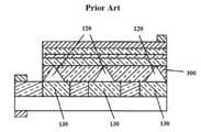
도 1은 종래의 3족 질화물 반도체 발광소자의 일 예를 나타내는 도면으로서, 3족 질화물 반도체 발광소자는 기판(100), 기판(100) 위에 성장되는 버퍼층(200), 버퍼층(200) 위에 성장되는 n형 3족 질화물 반도체층(300), n형 3족 질화물 반도체층(300) 위에 성장되는 활성층(400), 활성층(400) 위에 성장되는 p형 3족 질화물 반도체층(500), p형 3족 질화물 반도체층(500) 위에 형성되는 p측 전극(600), p측 전극(600) 위에 형성되는 p측 본딩 패드(700), p형 3족 질화물 반도체층(500)과 활성층(400)이 메사 식각되어 노출된 n형 3족 질화물 반도체층(300) 위에 형성되는 n측 전극(800), 그리고 보호막(900)을 포함한다.1 is a view illustrating an example of a conventional Group III nitride semiconductor light emitting device, wherein the Group III nitride semiconductor light emitting device is grown on the
기판(100)은 동종기판으로 GaN계 기판이 이용되며, 이종기판으로 사파이어 기판, SiC 기판 또는 Si 기판 등이 이용되지만, 3족 질화물 반도체층이 성장될 수 있는 기판이라면 어떠한 형태이어도 좋다. SiC 기판이 사용될 경우에 n측 전극(800)은 SiC 기판 측에 형성될 수 있다.As the
기판(100) 위에 성장되는 3족 질화물 반도체층들은 주로 MOCVD(유기금속기상성장법)에 의해 성장된다.Group III nitride semiconductor layers grown on the
버퍼층(200)은 이종기판(100)과 3족 질화물 반도체 사이의 격자상수 및 열팽창계수의 차이를 극복하기 위한 것이며, 미국특허 제5,122,845호에는 사파이어 기판 위에 380℃에서 800℃의 온도에서 100Å에서 500Å의 두께를 가지는 AlN 버퍼층을 성장시키는 기술이 기재되어 있으며, 미국특허 제5,290,393호에는 사파이어 기판 위에 200℃에서 900℃의 온도에서 10Å에서 5000Å의 두께를 가지는 Al(x)Ga(1-x)N (0≤x<1) 버퍼층을 성장시키는 기술이 기재되어 있고, 미국공개특허공보 제2006/154454호에는 600℃에서 990℃의 온도에서 SiC 버퍼층(씨앗층)을 성장시킨 다음 그 위에 In(x)Ga(1-x)N (0<x≤1) 층을 성장시키는 기술이 기재되어 있다. 바람 직하게는 n형 3족 질화물 반도체층(300)의 성장에 앞서 도핑되지 않는 GaN층이 성장되며, 이는 버퍼층(200)의 일부로 보아도 좋고, n형 3족 질화물 반도체층(300)의 일부로 보아도 좋다.The
n형 3족 질화물 반도체층(300)은 적어도 n측 전극(800)이 형성된 영역(n형 컨택층)이 불순물로 도핑되며, n형 컨택층은 바람직하게는 GaN로 이루어지고, Si으로 도핑된다. 미국특허 제5,733,796호에는 Si과 다른 소스 물질의 혼합비를 조절함으로써 원하는 도핑농도로 n형 컨택층을 도핑하는 기술이 기재되어 있다.In the n-type group III
활성층(400)은 전자와 정공의 재결합을 통해 광자(빛)를 생성하는 층으로서, 주로 In(x)Ga(1-x)N (0<x≤1)로 이루어지고, 하나의 양자우물층(single quantum well)이나 복수개의 양자우물층들(multi quantum wells)로 구성된다.The
p형 3족 질화물 반도체층(500)은 Mg과 같은 적절한 불순물을 이용해 도핑되며, 활성화(activation) 공정을 거쳐 p형 전도성을 가진다. 미국특허 제5,247,533호에는 전자빔 조사에 의해 p형 3족 질화물 반도체층을 활성화시키는 기술이 기재되어 있으며, 미국특허 제5,306,662호에는 400℃ 이상의 온도에서 열처리(annealing)함으로써 p형 3족 질화물 반도체층을 활성화시키는 기술이 기재되어 있고, 미국공개특허공보 제2006/157714호에는 p형 3족 질화물 반도체층 성장의 질소전구체로서 암모니아와 하이드라진계 소스 물질을 함께 사용함으로써 활성화 공정없이 p형 3족 질화물 반도체층이 p형 전도성을 가지게 하는 기술이 기재되어 있다.The p-type III-
p측 전극(600)은 p형 3족 질화물 반도체층(500) 전체로 전류가 잘 공급되도 록 하기 위해 구비되는 것이며, 미국특허 제5,563,422호에는 p형 3족 질화물 반도체층의 거의 전면에 걸쳐서 형성되며 p형 3족 질화물 반도체층(500)과 오믹접촉하고 Ni과 Au로 이루어진 투광성 전극(light-transmitting electrode)에 관한 기술이 기재되어 있으며, 미국특허 제6,515,306호에는 p형 3족 질화물 반도체층 위에 n형 초격자층을 형성한 다음 그 위에 ITO(Indium Tin Oxide)로 이루어진 투광성 전극을 형성한 기술이 기재되어 있다.The p-
한편, p측 전극(600)이 빛을 투과시키지 못하도록, 즉 빛을 기판 측으로 반사하도록 두꺼운 두께를 가지게 형성할 수 있는데, 이러한 기술을 플립칩(flip chip) 기술이라 한다. 미국특허 제6,194,743호에는 20nm 이상의 두께를 가지는 Ag 층, Ag 층을 덮는 확산 방지층, 그리고 확산 방지층을 덮는 Au와 Al으로 이루어진 본딩 층을 포함하는 전극 구조에 관한 기술이 기재되어 있다.On the other hand, the p-
p측 본딩 패드(700)와 n측 전극(800)은 전류의 공급과 외부로의 와이어 본딩을 위한 것이며, 미국특허 제5,563,422호에는 n측 전극을 Ti과 Al으로 구성한 기술이 기재되어 있다.The p-
보호막(900)은 이산화규소와 같은 물질로 형성되며, 생략될 수도 있다.The
한편, n형 3족 질화물 반도체층(300)이나 p형 3족 질화물 반도체층(500)은 단일의 층이나 복수개의 층으로 구성될 수 있으며, 최근에는 레이저 또는 습식 식각을 통해 기판(100)을 3족 질화물 반도체층들로부터 분리하여 수직형 발광소자를 제조하는 기술이 도입되고 있다.Meanwhile, the n-type III-
또한 기판(100)에 3족 질화물 반도체층을 성장하기에 앞서, 기판(100)에 패 턴을 형성하는 기술이 사용되고 있는데, 이는 3족 질화물 반도체층의 결정 결함을 감소시키거나 발광소자의 외부양자효율을 향상시키기 위한 것이다.In addition, prior to growing the group III nitride semiconductor layer on the
도 2는 미국특허공보 제6,335,546호 및 제7,115,486호에 기재된 발광소자의 일 예를 나타내는 도면으로서, 돌기(110)가 형성된 기판(100) 위에 3족 질화물 반도체층(200,300)을 측면 성장(Lateral Epitaxial Overgrowth)시킴으로써 결정 결함을 감소시키는 기술이 기재되어 있다. 3족 질화물 반도체층(200,300)이 측면 성장됨에 따라 기판(100)에는 공동(120; Cavity, Void or Air-Void)이 형성된다.FIG. 2 is a view illustrating one example of the light emitting devices described in US Patent Nos. 6,335,546 and 7,115,486, wherein the group III
도 3은 미국특허공보 제6,870,190호 및 제7,053,420호에 기재된 발광소자의 일 예를 나타내는 도면으로서, 패터닝된 기판(100) 상에서 3족 질화물 반도체층(300)이 성장되는 과정을 기재하고 있다. 3족 질화물 반도체층(300)은 패터닝된 기판(100)의 바닥면과 상면에서 성장을 시작한 다음, 성장된 3족 질화물 반도체층(300)이 만나게 되고, 만난 영역에서 성장이 촉진된 다음, 평탄한 면을 형성하게 된다. 이렇게 패터닝된 기판(100)을 이용함으로써, 빛을 스캐터링하여 외부양자효율을 높이는 한편, 결정 결함을 감소시켜 질화물 반도체층(300)의 질을 향상시키게 된다.FIG. 3 is a view illustrating one example of the light emitting devices described in US Patent Nos. 6,870,190 and 7,053,420, which describe a process of growing a group III
도 4는 미국특허공보 제6,870,191호 및 미국공개특허공보 제2005-082546호에 기재된 발광소자의 일 예를 나타내는 도면으로서, 둥근 종단면을 가지는(또는 상면에 평탄면이 없는) 돌기(110)가 형성된 기판(100) 위에 3족 질화물 반도체층(300)을 성장시킴으로써, 기판(100)의 바닥면에서만 3족 질화물 반도체층의 성장이 이루어지게 하여 보다 빨리 3족 질화물 반도체층(300)을 성장시키는 기술이 기재되어 있다.4 is a view showing an example of the light emitting device described in US Patent No. 6,870,191 and US Patent Publication No. 2005-082546, wherein the
도 5는 미국특허공보 제6,657,236호에 기재된 발광소자의 일 예를 나타내는 도면으로서, SiO2와 같은 마스크(130) 위에 3족 질화물 반도체층(300)을 성장시킴으로써, 공동(120)이 형성되게 하여 공동(120)이 발광소자 내부에서 빛을 스캐터링함으로써 발광소자의 외부양자효율을 높인 기술이 기재되어 있다.FIG. 5 is a view showing an example of a light emitting device described in US Patent No. 6,657,236, in which a
도 6은 미국특허공보 제5,491,350호 및 제6,657,236호에 기재된 발광소자의 일 예를 나타내는 도면으로서, 오목하게 패터닝된 기판(100) 상에서 3족 질화물 반도체층(300)을 성장시킴으로써, 기판(100)에 공동(120)이 형성되게 하여 공동(120)이 발광소자 내부에서 빛을 스캐터링함으로써 발광소자의 외부양자효율을 높인 기술이 기재되어 있다.FIG. 6 is a view showing examples of light emitting devices described in US Patent Nos. 5,491,350 and 6,657,236. The
그러나 도 6에 도시된 공동(120)의 경우에 도 5에 도시된 공동(120)과 달리, 3족 질화물 반도체층(300)과의 경계면에서의 곡률이 크지 않아, 스캐터링의 효과를 크게 기대하기가 어렵다.However, in the case of the
이에 대하여 '발명의 실시를 위한 구체적인 내용'의 후단에 기술한다.This will be described later in the Specification for Implementation of the Invention.
여기서는, 본 개시의 전체적인 요약(Summary)이 제공되며, 이것이 본 개시의 외연을 제한하는 것으로 이해되어는 아니된다(This section provides a general summary of the disclosure and is not a comprehensive disclosure of its full scope or all of its features).This section provides a general summary of the disclosure and is not a comprehensive disclosure of its full scope or all, provided that this is a summary of the disclosure. of its features).
본 개시에 따른 일 태양에 의하면(According to one aspect of the present disclosure), 돌기가 형성된 기판; 기판 위에 위치하며, 전자와 정공의 재결합을 통해 빛을 생성시키는 활성층을 구비하는 복수개의 3족 질화물 반도체층; 그리고, 복수개의 3족 질화물 반도체층에 형성되어 활성층에서 생성된 빛을 스캐터링하는 면;으로서, 돌기의 위에서 위로 볼록한 형상을 갖고, 복수개의 3족 질화물 반도체층이 식각되어 형성된 제1 면과, 복수개의 3족 질화물 반도체층의 성장에 의해 형성되어 제1 면에 연결된 제2 면을 구비하는 스캐터링 면;을 포함하는 것을 특징으로 하는 3족 질화물 반도체 발광소자가 제공된다.
본 개시에 따른 다른 태양에 의하면(According to one aspect of the present disclosure), 돌기가 형성된 기판; 기판 위에 위치하며, 전자와 정공의 재결합을 통해 빛을 생성시키는 활성층을 구비하는 복수개의 3족 질화물 반도체층; 그리고, 복수개의 3족 질화물 반도체층에 형성되어 활성층에서 생성된 빛을 스캐터링하는 면;으로서, 돌기의 위에서 위로 볼록한 형상을 갖고, 복수개의 3족 질화물 반도체층이 식각되어 형성된 제1 면과, 복수개의 3족 질화물 반도체층의 성장에 의해 형성되어 제1 면에 연결된 제2 면을 구비하는 스캐터링 면;을 포함하는 것을 특징으로 하는 3족 질화물 반도체 발광소자를 제조하는 방법이 제공된다.According to one aspect of the present disclosure, there is provided an according to one aspect of the present disclosure; A plurality of group III nitride semiconductor layers positioned on the substrate and having an active layer generating light through recombination of electrons and holes; And a surface formed on the plurality of Group 3 nitride semiconductor layers to scatter light generated in the active layer, the first surface having a convex shape from above the protrusion and formed by etching the plurality of Group 3 nitride semiconductor layers; And a scattering surface formed by growth of a plurality of group III nitride semiconductor layers, the scattering surface having a second surface connected to the first surface.
According to another aspect of the present disclosure (According to one aspect of the present disclosure), a substrate having protrusions formed thereon; A plurality of group III nitride semiconductor layers positioned on the substrate and having an active layer generating light through recombination of electrons and holes; And a surface formed on the plurality of Group 3 nitride semiconductor layers to scatter light generated in the active layer, the first surface having a convex shape from above the protrusion and formed by etching the plurality of Group 3 nitride semiconductor layers; And a scattering surface formed by growth of a plurality of group III nitride semiconductor layers, the second surface having a second surface connected to the first surface.
삭제delete
이에 대하여 '발명의 실시를 위한 구체적인 내용'의 후단에 기술한다.This will be described later in the Specification for Implementation of the Invention.
이하, 본 개시를 첨부된 도면을 참고로 하여 자세하게 설명한다(The present disclosure will now be described in detail with reference to the accompanying drawing(s)).The present disclosure will now be described in detail with reference to the accompanying drawing (s).
도 7은 본 개시에 따른 3족 질화물 반도체 발광소자의 일 예를 나타내는 도면으로서, 3족 질화물 반도체 발광소자는 기판(10), 기판(10) 위에 성장되는 버퍼층(20), 버퍼층(20) 위에 성장되는 n형 3족 질화물 반도체층(30), n형 3족 질화물 반도체층(30) 위에 성장되는 활성층(40), 활성층(40) 위에 성장되는 p형 3족 질화물 반도체층(50), p형 3족 질화물 반도체층(50) 위에 형성되는 p측 전극(60), p측 전극(60) 위에 형성되는 p측 본딩 패드(70), 그리고 p형 3족 질화물 반도체층(50)과 활성층(40)이 메사 식각되어 노출된 n형 3족 질화물 반도체층(30) 위에 형성되는 n측 전극(80)을 포함한다. 그리고, 기판(10)에는 둥근 돌기(11)가 형성되어 있으며, n형 3족 질화물 반도체층(30)의 아래에는 가공된 스캐터링 면(31)이 형성되어 있고, 돌기(11)와 가공된 스캐터링 면(31) 사이에는 공동(12)이 형성되어 있다. 따라서 본 개시에 따른 3족 질화물 반도체 발광소자에 의하면, 다른 굴절률을 가지는 3족 질화물 반도체층과 공동(12) 사이에 형성된 가공된 스캐터링 면(31) 및 다른 굴절률을 가지는 공동(12)과 기판(10) 사이에 형성된 돌기(11)에 의해 발광소자의 외부양자효율을 높일 수 있게 된다.7 is a diagram illustrating an example of a group III nitride semiconductor light emitting device according to the present disclosure, wherein the group III nitride semiconductor light emitting device is disposed on a
도 8은 본 개시에 따른 3족 질화물 반도체 발광소자를 제조하는 방법의 일 예를 설명하는 도면으로서, 먼저 돌기(11)가 형성된 기판(10)을 준비한다. 여기서 돌기(11)는 기판(10)을 에칭하여 형성할 수 있지만, SiO2와 같이 기판(10)과 다른 종류의 물질로 형성하는 것도 가능하다.8 is a view illustrating an example of a method of manufacturing a group III nitride semiconductor light emitting device according to the present disclosure. First, a
다음으로, 돌기(11)가 형성된 기판(10) 위에 1차 3족 질화물 반도체층(A)을 형성한다. 이때 돌기(11)의 상부가 노출되도록 한다. 이러한 관점에서, 돌기(11)의 형상에 특별한 제한이 있는 것은 아니며, 돌기(11)의 상부에서 1차 3족 질화물 반도체층(A)의 성장이 일어나지 않도록 종단면이 둥글거나 뾰족한(돌기 상부에 평탄면이 없는) 돌기(11)를 사용하는 것이 바람직하다. 예를 들어, (0001) 사파이어 기판을 사용하고, 1.2um의 높이, 3um의 바닥 직경을 가지는 돌기(돌기간 간격 1um)를 형성한 다음, 30nm의 버퍼층과 2um의 도핑되지 않은 GaN으로 1차 3족 질화물 반도체층(A)을 성장할 수 있다. (0001) 사파이어 기판 위에 도핑되지 않은 GaN이 성장될 때, 1차 3족 질화물 반도체층(A)은 {10-11}면(A1)이 노출된 형태를 가지며, 따라서 1차 3족 질화물 반도체층은 돌기의 상부에서 {10-11}면들로 된 구멍을 가진다(도 9 참조).Next, the primary group III nitride semiconductor layer A is formed on the
다음으로, 식각을 통해, 돌기(11)와 1차 3족 질화물 반도체층(A) 사이에 공간(15)이 형성되도록 한다. 식각은 고온의 인산 및 황산 혼합액, 고온의 KOH 용액, 또는 고온의 (COOH)2 (Oxalic acid) 등을 이용하여 행해질 수 있으며, 식각이 결정 품질이 나쁜 돌기(11)와 1차 3족 질화물 반도체층(A)의 계면에서 빠른 속도로 진행 되어 공간(15)이 형성된다. 이때 공간(15)의 모양과 두께 등은 식각 조건 및 돌기의 모양에 따라 영향을 받을 수 있다.Next, a
도 10은 식각 후 SEM을 통해 얻은 단면 사진으로서, 식각은 250℃의 온도에서, 인산:황산 = 3:1의 혼합액으로, 15초 동안 행해졌으며, 돌기(11)와 1차 질화물 반도체층(A) 사이에 공간(15)이 형성된 것을 나타내고 있다. 식각에 의해 상대적으로 에칭 속도가 낮은 {10-11} 결정면(A2)이 노출되어 있다.FIG. 10 is a cross-sectional image obtained through SEM after etching, and etching is performed for 15 seconds with a mixture of phosphoric acid: sulfuric acid = 3: 1 at a temperature of 250 ° C., and the
마지막으로, 2차 3족 질화물 반도체층(B)을 형성한다. 이 과정에서 공간(15)이 2차 3족 질화물 반도체층(B)의 횡방향 성장 모드에 의해 덮히게 되고, 닫힌 공동(12)이 형성된다. 2차 3족 질화물 반도체층(B)은 도핑되지 않은 GaN을 추가로 성장시킨 다음(예: 2um), 그 위에 도 7에 도시된 n형 3족 질화물 반도체층(30), 활성층(40) 그리고 p형 질화물 반도체층(50)을 성장시킴으로써 형성될 수 있다.Finally, the secondary group III nitride semiconductor layer (B) is formed. In this process, the
도 11은 2차 3족 질화물 반도체층 성장 후 SEM을 통해 얻은 단면 사진으로서, 돌기(11)와 1차 질화물 반도체층(A) 및 2차 질화물 반도체층(B)에 의해 둘러싸인 공동(12)이 잘 형성되어 있음을 알 수 있다. 가공된 스캐터링 면(31; 도 7 참조)은 식각 면(31a)과 에피성장에 의한 덮개 면(31b)으로 이루어져 있다.FIG. 11 is a cross-sectional photograph obtained by SEM after growth of the second group III nitride semiconductor layer, wherein the
이하 본 개시의 다양한 실시 형태에 대하여 설명한다.Various embodiments of the present disclosure will be described below.
(1) 폐곡면 형태의 스캐터링 면과 기판 사이에 위치하는 돌기를 구비하는 3족 질화물 반도체 발광소자.(1) A group III nitride semiconductor light emitting device comprising a projection located between a scattering surface having a closed curved shape and a substrate.
(2) 스캐터링 면이 돌기의 위에서 위로 볼록한 형상인 3족 질화물 반도체 발광소자.(2) A group III nitride semiconductor light emitting element having a scattering surface convex upward from the projection.
(3) 식각에 의해 형성되는 공동의 아래에 위치하며, 기판과 다른 물질로 된 돌기를 구비하는 3족 질화물 반도체 발광소자. 예를 들어, 돌기가 SiO2와 같은 실리콘옥사이드로 이루어지는 경우에, 돌기 위에서 성장이 일어나지 않으므로, 상부가 평탄한 형태의 돌기를 이용하더라도, 3족 질화물 반도체층의 성장시에 용이하게 돌기의 상부를 노출시킬 수 있게 된다.(3) A group III nitride semiconductor light emitting element located below the cavity formed by etching, and having a projection made of a material different from the substrate. For example, in the case where the projections are made of silicon oxide such as SiO2 , no growth occurs on the projections, and therefore, even when the projections have a flat shape, the upper portions of the projections are easily exposed during the growth of the group III nitride semiconductor layer. You can do it.
(4) 3족 질화물 반도체층으로 된 덮개 층을 가지는 스캐터링 면을 구비하는 3족 질화물 반도체 발광소자.(4) A group III nitride semiconductor light emitting element having a scattering surface having a covering layer of a group III nitride semiconductor layer.
(5) 식각과 에피성장을 통해 형성된 스캐터링 면을 구비하는 3족 질화물 반도체 발광소자를 제조하는 방법.(5) A method of manufacturing a group III nitride semiconductor light emitting device having a scattering surface formed through etching and epitaxial growth.
본 개시에 따른 하나의 3족 질화물 반도체 발광소자에 의하면, 발광소자의 외부양자효율을 높일 수 있게 된다.According to one group III nitride semiconductor light emitting device according to the present disclosure, it is possible to increase the external quantum efficiency of the light emitting device.
또한 본 개시에 따른 다른 하나의 3족 질화물 반도체 발광소자에 의하면, 큰 곡률을 가지는 공동을 이용함으로써, 발광소자의 외부양자효율을 높일 수 있게 된다.In addition, according to another group III nitride semiconductor light emitting device according to the present disclosure, by using a cavity having a large curvature, the external quantum efficiency of the light emitting device can be increased.
도 1은 종래의 3족 질화물 반도체 발광소자의 일 예를 나타내는 도면,1 is a view showing an example of a conventional group III nitride semiconductor light emitting device,
도 2는 미국특허공보 제6,335,546호 및 제7,115,486호에 기재된 발광소자의 일 예를 나타내는 도면으로서,FIG. 2 is a view showing an example of light emitting devices described in US Patent Nos. 6,335,546 and 7,115,486.
도 3은 미국특허공보 제6,870,190호 및 제7,053,420호에 기재된 발광소자의 일 예를 나타내는 도면으로서,3 is a view showing an example of light emitting devices described in US Patent Nos. 6,870,190 and 7,053,420.
도 4는 미국특허공보 제6,870,191호 및 미국공개특허공보 제2005-082546호에 기재된 발광소자의 일 예를 나타내는 도면으로서,4 is a view showing an example of a light emitting device described in US Patent No. 6,870,191 and US Patent Publication No. 2005-082546,
도 5는 미국특허공보 제6,657,236호에 기재된 발광소자의 일 예를 나타내는 도면으로서,5 is a view showing an example of a light emitting device described in US Patent No. 6,657,236,
도 6은 미국특허공보 제5,491,350호 및 제6,657,236호에 기재된 발광소자의 일 예를 나타내는 도면으로서,6 is a view showing an example of the light emitting device described in US Patent Nos. 5,491,350 and 6,657,236.
도 7은 본 개시에 따른 3족 질화물 반도체 발광소자의 일 예를 나타내는 도면,7 is a view showing an example of a group III nitride semiconductor light emitting device according to the present disclosure;
도 8은 본 개시에 따른 3족 질화물 반도체 발광소자를 제조하는 방법의 일 예를 설명하는 도면,8 is a view for explaining an example of a method of manufacturing a group III nitride semiconductor light emitting device according to the present disclosure;
도 9는 1차 3족 질화물 반도체층의 성장 후 위에서 본 기판의 일 예를 나타내는 현미경 표면 사진,9 is a microscopic surface photograph showing an example of a substrate seen from above after growth of a primary group III nitride semiconductor layer;
도 10은 식각 후 SEM을 통해 얻은 단면 사진,10 is a cross-sectional photograph obtained by SEM after etching,
도 11은 2차 3족 질화물 반도체층 성장 후 SEM을 통해 얻은 단면 사진.Figure 11 is a cross-sectional photograph obtained by SEM after the growth of the second group III nitride semiconductor layer.
Claims (10)
Translated fromKoreanPriority Applications (3)
| Application Number | Priority Date | Filing Date | Title |
|---|---|---|---|
| KR1020080101155AKR101009651B1 (en) | 2008-10-15 | 2008-10-15 | Group III nitride semiconductor light emitting device |
| PCT/KR2009/005706WO2010044561A2 (en) | 2008-10-15 | 2009-10-07 | Group iii nitride semiconductor light emitting device |
| US12/648,692US20100102353A1 (en) | 2008-10-15 | 2009-12-29 | III-Nitride Semiconductor Light Emitting Device |
Applications Claiming Priority (1)
| Application Number | Priority Date | Filing Date | Title |
|---|---|---|---|
| KR1020080101155AKR101009651B1 (en) | 2008-10-15 | 2008-10-15 | Group III nitride semiconductor light emitting device |
Publications (2)
| Publication Number | Publication Date |
|---|---|
| KR20100042041A KR20100042041A (en) | 2010-04-23 |
| KR101009651B1true KR101009651B1 (en) | 2011-01-19 |
Family
ID=42107018
Family Applications (1)
| Application Number | Title | Priority Date | Filing Date |
|---|---|---|---|
| KR1020080101155AExpired - Fee RelatedKR101009651B1 (en) | 2008-10-15 | 2008-10-15 | Group III nitride semiconductor light emitting device |
Country Status (3)
| Country | Link |
|---|---|
| US (1) | US20100102353A1 (en) |
| KR (1) | KR101009651B1 (en) |
| WO (1) | WO2010044561A2 (en) |
Families Citing this family (20)
| Publication number | Priority date | Publication date | Assignee | Title |
|---|---|---|---|---|
| KR101008285B1 (en)* | 2005-10-28 | 2011-01-13 | 주식회사 에피밸리 | Group III nitride semiconductor light emitting device |
| US8476658B2 (en)* | 2009-11-25 | 2013-07-02 | Jing Jie Dai | Semiconductor light-emitting devices |
| KR100993093B1 (en) | 2010-02-04 | 2010-11-08 | 엘지이노텍 주식회사 | Light emitting device package |
| EP2403019B1 (en)* | 2010-06-29 | 2017-02-22 | LG Innotek Co., Ltd. | Light emitting device |
| US9245760B2 (en) | 2010-09-30 | 2016-01-26 | Infineon Technologies Ag | Methods of forming epitaxial layers on a porous semiconductor layer |
| EP2509120A1 (en) | 2011-04-05 | 2012-10-10 | Imec | Semiconductor device and method |
| JP5875249B2 (en)* | 2011-04-28 | 2016-03-02 | ソウル バイオシス カンパニー リミテッドSeoul Viosys Co.,Ltd. | Semiconductor substrate, semiconductor device and manufacturing method thereof |
| KR101259999B1 (en)* | 2011-04-28 | 2013-05-06 | 서울옵토디바이스주식회사 | Semiconductor substrate and method of fabricating the same |
| TW201248725A (en)* | 2011-05-31 | 2012-12-01 | Aceplux Optotech Inc | Epitaxial substrate with transparent cone, LED, and manufacturing method thereof. |
| TWI528579B (en)* | 2012-04-18 | 2016-04-01 | 新世紀光電股份有限公司 | Light emitting diode device |
| WO2014025003A1 (en)* | 2012-08-06 | 2014-02-13 | 日本碍子株式会社 | Composite substrate and functional element |
| TWI565094B (en)* | 2012-11-15 | 2017-01-01 | 財團法人工業技術研究院 | Nitride semiconductor structure |
| CN103165771B (en)* | 2013-03-28 | 2015-07-15 | 天津三安光电有限公司 | Nitride bottom layer with embedded hole structure and preparation method of nitride bottom layer |
| US9362452B2 (en)* | 2013-06-14 | 2016-06-07 | Epistar Corporation | Light-emitting device and the manufacturing method thereof |
| US20140367693A1 (en)* | 2013-06-14 | 2014-12-18 | Epistar Corporation | Light-emitting device and the manufacturing method thereof |
| WO2015025631A1 (en)* | 2013-08-21 | 2015-02-26 | シャープ株式会社 | Nitride semiconductor light-emitting element |
| TWI597863B (en)* | 2013-10-22 | 2017-09-01 | 晶元光電股份有限公司 | Light-emitting element and method of manufacturing same |
| KR102284535B1 (en)* | 2014-11-12 | 2021-08-02 | 서울바이오시스 주식회사 | Light emitting device and method of making the same |
| JP2016066814A (en)* | 2015-12-22 | 2016-04-28 | 株式会社東芝 | Semiconductor light emitting device, nitride semiconductor layer growth substrate, and nitride semiconductor wafer |
| KR102591149B1 (en)* | 2021-12-20 | 2023-10-19 | 웨이브로드 주식회사 | Method of manufacturing a non emitting iii-nitride semiconductor stacked structure |
Citations (4)
| Publication number | Priority date | Publication date | Assignee | Title |
|---|---|---|---|---|
| JP2002164296A (en) | 2000-09-18 | 2002-06-07 | Mitsubishi Cable Ind Ltd | Semiconductor substrate and method of manufacturing the same |
| KR20050062832A (en)* | 2003-12-18 | 2005-06-28 | 삼성코닝 주식회사 | Preparation of nitride semiconductor template for light emitter |
| US7052979B2 (en) | 2001-02-14 | 2006-05-30 | Toyoda Gosei Co., Ltd. | Production method for semiconductor crystal and semiconductor luminous element |
| KR100863804B1 (en) | 2007-04-19 | 2008-10-16 | 고려대학교 산학협력단 | Nitride light emitting device and its manufacturing method |
Family Cites Families (26)
| Publication number | Priority date | Publication date | Assignee | Title |
|---|---|---|---|---|
| JP3026087B2 (en)* | 1989-03-01 | 2000-03-27 | 豊田合成株式会社 | Gas phase growth method of gallium nitride based compound semiconductor |
| CA2037198C (en)* | 1990-02-28 | 1996-04-23 | Katsuhide Manabe | Light-emitting semiconductor device using gallium nitride group compound |
| JP3160914B2 (en)* | 1990-12-26 | 2001-04-25 | 豊田合成株式会社 | Gallium nitride based compound semiconductor laser diode |
| US5290393A (en)* | 1991-01-31 | 1994-03-01 | Nichia Kagaku Kogyo K.K. | Crystal growth method for gallium nitride-based compound semiconductor |
| US5306662A (en)* | 1991-11-08 | 1994-04-26 | Nichia Chemical Industries, Ltd. | Method of manufacturing P-type compound semiconductor |
| EP0622858B2 (en)* | 1993-04-28 | 2004-09-29 | Nichia Corporation | Gallium nitride-based III-V group compound semiconductor device and method of producing the same |
| TW253999B (en)* | 1993-06-30 | 1995-08-11 | Hitachi Cable | |
| EP1928034A3 (en)* | 1997-12-15 | 2008-06-18 | Philips Lumileds Lighting Company LLC | Light emitting device |
| US6335546B1 (en)* | 1998-07-31 | 2002-01-01 | Sharp Kabushiki Kaisha | Nitride semiconductor structure, method for producing a nitride semiconductor structure, and light emitting device |
| WO2000055893A1 (en)* | 1999-03-17 | 2000-09-21 | Mitsubishi Cable Industries, Ltd. | Semiconductor base and its manufacturing method, and semiconductor crystal manufacturing method |
| KR100700993B1 (en)* | 1999-12-03 | 2007-03-30 | 크리, 인코포레이티드 | Light emitting diode having improved light extraction structure and manufacturing method thereof |
| JP4780113B2 (en)* | 2000-09-18 | 2011-09-28 | 三菱化学株式会社 | Semiconductor light emitting device |
| TW488088B (en)* | 2001-01-19 | 2002-05-21 | South Epitaxy Corp | Light emitting diode structure |
| JP3690340B2 (en)* | 2001-03-06 | 2005-08-31 | ソニー株式会社 | Semiconductor light emitting device and manufacturing method thereof |
| CN1284250C (en)* | 2001-03-21 | 2006-11-08 | 三菱电线工业株式会社 | Semiconductor light emitting element |
| JP4055503B2 (en)* | 2001-07-24 | 2008-03-05 | 日亜化学工業株式会社 | Semiconductor light emitting device |
| US7601553B2 (en)* | 2003-07-18 | 2009-10-13 | Epivalley Co., Ltd. | Method of manufacturing a gallium nitride semiconductor light emitting device |
| KR100714639B1 (en)* | 2003-10-21 | 2007-05-07 | 삼성전기주식회사 | Light emitting element |
| KR100448352B1 (en)* | 2003-11-28 | 2004-09-10 | 삼성전기주식회사 | Method for fabricating GaN-based nitride layer |
| US7342261B2 (en)* | 2005-05-16 | 2008-03-11 | Dong-Sing Wuu | Light emitting device |
| US7795600B2 (en)* | 2006-03-24 | 2010-09-14 | Goldeneye, Inc. | Wavelength conversion chip for use with light emitting diodes and method for making same |
| KR100786777B1 (en)* | 2006-03-28 | 2007-12-18 | 전북대학교산학협력단 | Method of manufacturing a semiconductor structure |
| KR100809227B1 (en)* | 2006-10-27 | 2008-03-05 | 삼성전기주식회사 | Nitride semiconductor light emitting device and manufacturing method |
| KR100916375B1 (en)* | 2007-06-27 | 2009-09-07 | 주식회사 에피밸리 | Method of manufacturing semiconductor light emitting device and semiconductor light emitting device |
| WO2009002129A2 (en)* | 2007-06-27 | 2008-12-31 | Epivalley Co., Ltd. | Semiconductor light emitting device and method of manufacturing the same |
| JP5045418B2 (en)* | 2007-11-28 | 2012-10-10 | 三菱化学株式会社 | GaN-based LED element, GaN-based LED element manufacturing method, and GaN-based LED element manufacturing template |
- 2008
- 2008-10-15KRKR1020080101155Apatent/KR101009651B1/ennot_activeExpired - Fee Related
- 2009
- 2009-10-07WOPCT/KR2009/005706patent/WO2010044561A2/enactiveApplication Filing
- 2009-12-29USUS12/648,692patent/US20100102353A1/ennot_activeAbandoned
Patent Citations (4)
| Publication number | Priority date | Publication date | Assignee | Title |
|---|---|---|---|---|
| JP2002164296A (en) | 2000-09-18 | 2002-06-07 | Mitsubishi Cable Ind Ltd | Semiconductor substrate and method of manufacturing the same |
| US7052979B2 (en) | 2001-02-14 | 2006-05-30 | Toyoda Gosei Co., Ltd. | Production method for semiconductor crystal and semiconductor luminous element |
| KR20050062832A (en)* | 2003-12-18 | 2005-06-28 | 삼성코닝 주식회사 | Preparation of nitride semiconductor template for light emitter |
| KR100863804B1 (en) | 2007-04-19 | 2008-10-16 | 고려대학교 산학협력단 | Nitride light emitting device and its manufacturing method |
Also Published As
| Publication number | Publication date |
|---|---|
| US20100102353A1 (en) | 2010-04-29 |
| WO2010044561A3 (en) | 2010-08-05 |
| WO2010044561A2 (en) | 2010-04-22 |
| KR20100042041A (en) | 2010-04-23 |
Similar Documents
| Publication | Publication Date | Title |
|---|---|---|
| KR101009651B1 (en) | Group III nitride semiconductor light emitting device | |
| KR100541102B1 (en) | Nitride semiconductor light emitting device having improved ohmic contact and manufacturing method thereof | |
| KR100956456B1 (en) | Group III nitride semiconductor light emitting device | |
| KR20090064903A (en) | Group III nitride semiconductor light emitting device | |
| KR20110018563A (en) | Group III nitride semiconductor light emitting device and method of manufacturing the same | |
| KR101199187B1 (en) | Light emitting diode and fabricating method thereof | |
| KR101000277B1 (en) | Semiconductor light emitting device | |
| KR100960278B1 (en) | Group III nitride semiconductor light emitting device and manufacturing method | |
| KR100957742B1 (en) | Group III nitride semiconductor light emitting device | |
| US20100289036A1 (en) | Iii-nitride semiconductor light emitting device and method for manufacturing the same | |
| KR100661960B1 (en) | Light emitting diodes and manufacturing method thereof | |
| KR101197686B1 (en) | Iii-nitride semiconductor light emitting device | |
| KR101098589B1 (en) | Iii-nitride semiconductor light emitting device | |
| KR101120006B1 (en) | Vertical semiconductor light emitting device and method for fabricating the same | |
| KR20090117865A (en) | Group III nitride semiconductor light emitting device | |
| KR20100012003A (en) | Iii-nitride semiconductor light emitting device | |
| KR100743468B1 (en) | Group III nitride semiconductor light emitting device | |
| KR101009653B1 (en) | Group III nitride semiconductor light emitting device | |
| KR101009652B1 (en) | Group III nitride semiconductor light emitting device | |
| KR20080020206A (en) | Group III nitride semiconductor light emitting device | |
| KR101034764B1 (en) | Method of manufacturing group III nitride semiconductor light emitting device | |
| KR101062754B1 (en) | Semiconductor light emitting device | |
| KR101008286B1 (en) | Group III nitride semiconductor light emitting device | |
| KR20110077363A (en) | Group III nitride semiconductor light emitting device | |
| US20100102338A1 (en) | III-Nitride Semiconductor Light Emitting Device |
Legal Events
| Date | Code | Title | Description |
|---|---|---|---|
| A201 | Request for examination | ||
| PA0109 | Patent application | St.27 status event code:A-0-1-A10-A12-nap-PA0109 | |
| PA0201 | Request for examination | St.27 status event code:A-1-2-D10-D11-exm-PA0201 | |
| R18-X000 | Changes to party contact information recorded | St.27 status event code:A-3-3-R10-R18-oth-X000 | |
| D13-X000 | Search requested | St.27 status event code:A-1-2-D10-D13-srh-X000 | |
| D14-X000 | Search report completed | St.27 status event code:A-1-2-D10-D14-srh-X000 | |
| PG1501 | Laying open of application | St.27 status event code:A-1-1-Q10-Q12-nap-PG1501 | |
| PN2301 | Change of applicant | St.27 status event code:A-3-3-R10-R13-asn-PN2301 St.27 status event code:A-3-3-R10-R11-asn-PN2301 | |
| E902 | Notification of reason for refusal | ||
| PE0902 | Notice of grounds for rejection | St.27 status event code:A-1-2-D10-D21-exm-PE0902 | |
| E13-X000 | Pre-grant limitation requested | St.27 status event code:A-2-3-E10-E13-lim-X000 | |
| P11-X000 | Amendment of application requested | St.27 status event code:A-2-2-P10-P11-nap-X000 | |
| P13-X000 | Application amended | St.27 status event code:A-2-2-P10-P13-nap-X000 | |
| E701 | Decision to grant or registration of patent right | ||
| PE0701 | Decision of registration | St.27 status event code:A-1-2-D10-D22-exm-PE0701 | |
| GRNT | Written decision to grant | ||
| PR0701 | Registration of establishment | St.27 status event code:A-2-4-F10-F11-exm-PR0701 | |
| PR1002 | Payment of registration fee | St.27 status event code:A-2-2-U10-U11-oth-PR1002 Fee payment year number:1 | |
| PG1601 | Publication of registration | St.27 status event code:A-4-4-Q10-Q13-nap-PG1601 | |
| PN2301 | Change of applicant | St.27 status event code:A-5-5-R10-R13-asn-PN2301 St.27 status event code:A-5-5-R10-R11-asn-PN2301 | |
| PN2301 | Change of applicant | St.27 status event code:A-5-5-R10-R13-asn-PN2301 St.27 status event code:A-5-5-R10-R11-asn-PN2301 | |
| PN2301 | Change of applicant | St.27 status event code:A-5-5-R10-R13-asn-PN2301 St.27 status event code:A-5-5-R10-R11-asn-PN2301 | |
| FPAY | Annual fee payment | Payment date:20140113 Year of fee payment:4 | |
| PR1001 | Payment of annual fee | St.27 status event code:A-4-4-U10-U11-oth-PR1001 Fee payment year number:4 | |
| FPAY | Annual fee payment | Payment date:20150114 Year of fee payment:5 | |
| PR1001 | Payment of annual fee | St.27 status event code:A-4-4-U10-U11-oth-PR1001 Fee payment year number:5 | |
| FPAY | Annual fee payment | Payment date:20160114 Year of fee payment:6 | |
| PR1001 | Payment of annual fee | St.27 status event code:A-4-4-U10-U11-oth-PR1001 Fee payment year number:6 | |
| FPAY | Annual fee payment | Payment date:20170116 Year of fee payment:7 | |
| PR1001 | Payment of annual fee | St.27 status event code:A-4-4-U10-U11-oth-PR1001 Fee payment year number:7 | |
| R18-X000 | Changes to party contact information recorded | St.27 status event code:A-5-5-R10-R18-oth-X000 | |
| PR1001 | Payment of annual fee | St.27 status event code:A-4-4-U10-U11-oth-PR1001 Fee payment year number:8 | |
| PC1903 | Unpaid annual fee | St.27 status event code:A-4-4-U10-U13-oth-PC1903 Not in force date:20190114 Payment event data comment text:Termination Category : DEFAULT_OF_REGISTRATION_FEE | |
| K11-X000 | Ip right revival requested | St.27 status event code:A-6-4-K10-K11-oth-X000 | |
| PC1903 | Unpaid annual fee | St.27 status event code:N-4-6-H10-H13-oth-PC1903 Ip right cessation event data comment text:Termination Category : DEFAULT_OF_REGISTRATION_FEE Not in force date:20190114 | |
| PR0401 | Registration of restoration | St.27 status event code:A-6-4-K10-K13-oth-PR0401 | |
| PR1001 | Payment of annual fee | St.27 status event code:A-4-4-U10-U11-oth-PR1001 Fee payment year number:9 | |
| FPAY | Annual fee payment | Payment date:20200107 Year of fee payment:10 | |
| PR1001 | Payment of annual fee | St.27 status event code:A-4-4-U10-U11-oth-PR1001 Fee payment year number:10 | |
| PC1903 | Unpaid annual fee | St.27 status event code:A-4-4-U10-U13-oth-PC1903 Not in force date:20210114 Payment event data comment text:Termination Category : DEFAULT_OF_REGISTRATION_FEE | |
| PC1903 | Unpaid annual fee | St.27 status event code:N-4-6-H10-H13-oth-PC1903 Ip right cessation event data comment text:Termination Category : DEFAULT_OF_REGISTRATION_FEE Not in force date:20210114 | |
| P22-X000 | Classification modified | St.27 status event code:A-4-4-P10-P22-nap-X000 |