KR101009123B1 - Manufacturing Method of Semiconductor Device - Google Patents
Manufacturing Method of Semiconductor DeviceDownload PDFInfo
- Publication number
- KR101009123B1 KR101009123B1KR1020090004927AKR20090004927AKR101009123B1KR 101009123 B1KR101009123 B1KR 101009123B1KR 1020090004927 AKR1020090004927 AKR 1020090004927AKR 20090004927 AKR20090004927 AKR 20090004927AKR 101009123 B1KR101009123 B1KR 101009123B1
- Authority
- KR
- South Korea
- Prior art keywords
- insulating film
- layer
- wiring
- metal layer
- opening
- Prior art date
- Legal status (The legal status is an assumption and is not a legal conclusion. Google has not performed a legal analysis and makes no representation as to the accuracy of the status listed.)
- Expired - Fee Related
Links
Images


Classifications
- H—ELECTRICITY
- H01—ELECTRIC ELEMENTS
- H01L—SEMICONDUCTOR DEVICES NOT COVERED BY CLASS H10
- H01L23/00—Details of semiconductor or other solid state devices
- H01L23/52—Arrangements for conducting electric current within the device in operation from one component to another, i.e. interconnections, e.g. wires, lead frames
- H01L23/538—Arrangements for conducting electric current within the device in operation from one component to another, i.e. interconnections, e.g. wires, lead frames the interconnection structure between a plurality of semiconductor chips being formed on, or in, insulating substrates
- H01L23/5389—Arrangements for conducting electric current within the device in operation from one component to another, i.e. interconnections, e.g. wires, lead frames the interconnection structure between a plurality of semiconductor chips being formed on, or in, insulating substrates the chips being integrally enclosed by the interconnect and support structures
- H—ELECTRICITY
- H01—ELECTRIC ELEMENTS
- H01L—SEMICONDUCTOR DEVICES NOT COVERED BY CLASS H10
- H01L23/00—Details of semiconductor or other solid state devices
- H01L23/12—Mountings, e.g. non-detachable insulating substrates
- H—ELECTRICITY
- H01—ELECTRIC ELEMENTS
- H01L—SEMICONDUCTOR DEVICES NOT COVERED BY CLASS H10
- H01L24/00—Arrangements for connecting or disconnecting semiconductor or solid-state bodies; Methods or apparatus related thereto
- H01L24/01—Means for bonding being attached to, or being formed on, the surface to be connected, e.g. chip-to-package, die-attach, "first-level" interconnects; Manufacturing methods related thereto
- H01L24/18—High density interconnect [HDI] connectors; Manufacturing methods related thereto
- H01L24/19—Manufacturing methods of high density interconnect preforms
- H—ELECTRICITY
- H01—ELECTRIC ELEMENTS
- H01L—SEMICONDUCTOR DEVICES NOT COVERED BY CLASS H10
- H01L24/00—Arrangements for connecting or disconnecting semiconductor or solid-state bodies; Methods or apparatus related thereto
- H01L24/80—Methods for connecting semiconductor or other solid state bodies using means for bonding being attached to, or being formed on, the surface to be connected
- H01L24/82—Methods for connecting semiconductor or other solid state bodies using means for bonding being attached to, or being formed on, the surface to be connected by forming build-up interconnects at chip-level, e.g. for high density interconnects [HDI]
- H—ELECTRICITY
- H01—ELECTRIC ELEMENTS
- H01L—SEMICONDUCTOR DEVICES NOT COVERED BY CLASS H10
- H01L25/00—Assemblies consisting of a plurality of semiconductor or other solid state devices
- H01L25/18—Assemblies consisting of a plurality of semiconductor or other solid state devices the devices being of the types provided for in two or more different main groups of the same subclass of H10B, H10D, H10F, H10H, H10K or H10N
- H—ELECTRICITY
- H01—ELECTRIC ELEMENTS
- H01L—SEMICONDUCTOR DEVICES NOT COVERED BY CLASS H10
- H01L21/00—Processes or apparatus adapted for the manufacture or treatment of semiconductor or solid state devices or of parts thereof
- H01L21/02—Manufacture or treatment of semiconductor devices or of parts thereof
- H01L21/04—Manufacture or treatment of semiconductor devices or of parts thereof the devices having potential barriers, e.g. a PN junction, depletion layer or carrier concentration layer
- H01L21/50—Assembly of semiconductor devices using processes or apparatus not provided for in a single one of the groups H01L21/18 - H01L21/326 or H10D48/04 - H10D48/07 e.g. sealing of a cap to a base of a container
- H01L21/56—Encapsulations, e.g. encapsulation layers, coatings
- H01L21/568—Temporary substrate used as encapsulation process aid
- H—ELECTRICITY
- H01—ELECTRIC ELEMENTS
- H01L—SEMICONDUCTOR DEVICES NOT COVERED BY CLASS H10
- H01L2224/00—Indexing scheme for arrangements for connecting or disconnecting semiconductor or solid-state bodies and methods related thereto as covered by H01L24/00
- H01L2224/01—Means for bonding being attached to, or being formed on, the surface to be connected, e.g. chip-to-package, die-attach, "first-level" interconnects; Manufacturing methods related thereto
- H01L2224/02—Bonding areas; Manufacturing methods related thereto
- H01L2224/04—Structure, shape, material or disposition of the bonding areas prior to the connecting process
- H01L2224/0401—Bonding areas specifically adapted for bump connectors, e.g. under bump metallisation [UBM]
- H—ELECTRICITY
- H01—ELECTRIC ELEMENTS
- H01L—SEMICONDUCTOR DEVICES NOT COVERED BY CLASS H10
- H01L2224/00—Indexing scheme for arrangements for connecting or disconnecting semiconductor or solid-state bodies and methods related thereto as covered by H01L24/00
- H01L2224/01—Means for bonding being attached to, or being formed on, the surface to be connected, e.g. chip-to-package, die-attach, "first-level" interconnects; Manufacturing methods related thereto
- H01L2224/02—Bonding areas; Manufacturing methods related thereto
- H01L2224/04—Structure, shape, material or disposition of the bonding areas prior to the connecting process
- H01L2224/04105—Bonding areas formed on an encapsulation of the semiconductor or solid-state body, e.g. bonding areas on chip-scale packages
- H—ELECTRICITY
- H01—ELECTRIC ELEMENTS
- H01L—SEMICONDUCTOR DEVICES NOT COVERED BY CLASS H10
- H01L2224/00—Indexing scheme for arrangements for connecting or disconnecting semiconductor or solid-state bodies and methods related thereto as covered by H01L24/00
- H01L2224/01—Means for bonding being attached to, or being formed on, the surface to be connected, e.g. chip-to-package, die-attach, "first-level" interconnects; Manufacturing methods related thereto
- H01L2224/10—Bump connectors; Manufacturing methods related thereto
- H01L2224/12—Structure, shape, material or disposition of the bump connectors prior to the connecting process
- H01L2224/12105—Bump connectors formed on an encapsulation of the semiconductor or solid-state body, e.g. bumps on chip-scale packages
- H—ELECTRICITY
- H01—ELECTRIC ELEMENTS
- H01L—SEMICONDUCTOR DEVICES NOT COVERED BY CLASS H10
- H01L2224/00—Indexing scheme for arrangements for connecting or disconnecting semiconductor or solid-state bodies and methods related thereto as covered by H01L24/00
- H01L2224/01—Means for bonding being attached to, or being formed on, the surface to be connected, e.g. chip-to-package, die-attach, "first-level" interconnects; Manufacturing methods related thereto
- H01L2224/10—Bump connectors; Manufacturing methods related thereto
- H01L2224/15—Structure, shape, material or disposition of the bump connectors after the connecting process
- H01L2224/16—Structure, shape, material or disposition of the bump connectors after the connecting process of an individual bump connector
- H01L2224/161—Disposition
- H01L2224/16135—Disposition the bump connector connecting between different semiconductor or solid-state bodies, i.e. chip-to-chip
- H01L2224/16145—Disposition the bump connector connecting between different semiconductor or solid-state bodies, i.e. chip-to-chip the bodies being stacked
- H—ELECTRICITY
- H01—ELECTRIC ELEMENTS
- H01L—SEMICONDUCTOR DEVICES NOT COVERED BY CLASS H10
- H01L2224/00—Indexing scheme for arrangements for connecting or disconnecting semiconductor or solid-state bodies and methods related thereto as covered by H01L24/00
- H01L2224/01—Means for bonding being attached to, or being formed on, the surface to be connected, e.g. chip-to-package, die-attach, "first-level" interconnects; Manufacturing methods related thereto
- H01L2224/18—High density interconnect [HDI] connectors; Manufacturing methods related thereto
- H01L2224/19—Manufacturing methods of high density interconnect preforms
- H—ELECTRICITY
- H01—ELECTRIC ELEMENTS
- H01L—SEMICONDUCTOR DEVICES NOT COVERED BY CLASS H10
- H01L2224/00—Indexing scheme for arrangements for connecting or disconnecting semiconductor or solid-state bodies and methods related thereto as covered by H01L24/00
- H01L2224/01—Means for bonding being attached to, or being formed on, the surface to be connected, e.g. chip-to-package, die-attach, "first-level" interconnects; Manufacturing methods related thereto
- H01L2224/18—High density interconnect [HDI] connectors; Manufacturing methods related thereto
- H01L2224/23—Structure, shape, material or disposition of the high density interconnect connectors after the connecting process
- H01L2224/24—Structure, shape, material or disposition of the high density interconnect connectors after the connecting process of an individual high density interconnect connector
- H01L2224/241—Disposition
- H01L2224/24151—Connecting between a semiconductor or solid-state body and an item not being a semiconductor or solid-state body, e.g. chip-to-substrate, chip-to-passive
- H01L2224/24221—Connecting between a semiconductor or solid-state body and an item not being a semiconductor or solid-state body, e.g. chip-to-substrate, chip-to-passive the body and the item being stacked
- H01L2224/24225—Connecting between a semiconductor or solid-state body and an item not being a semiconductor or solid-state body, e.g. chip-to-substrate, chip-to-passive the body and the item being stacked the item being non-metallic, e.g. insulating substrate with or without metallisation
- H01L2224/24227—Connecting between a semiconductor or solid-state body and an item not being a semiconductor or solid-state body, e.g. chip-to-substrate, chip-to-passive the body and the item being stacked the item being non-metallic, e.g. insulating substrate with or without metallisation the HDI interconnect not connecting to the same level of the item at which the semiconductor or solid-state body is mounted, e.g. the semiconductor or solid-state body being mounted in a cavity or on a protrusion of the item
- H—ELECTRICITY
- H01—ELECTRIC ELEMENTS
- H01L—SEMICONDUCTOR DEVICES NOT COVERED BY CLASS H10
- H01L2224/00—Indexing scheme for arrangements for connecting or disconnecting semiconductor or solid-state bodies and methods related thereto as covered by H01L24/00
- H01L2224/01—Means for bonding being attached to, or being formed on, the surface to be connected, e.g. chip-to-package, die-attach, "first-level" interconnects; Manufacturing methods related thereto
- H01L2224/26—Layer connectors, e.g. plate connectors, solder or adhesive layers; Manufacturing methods related thereto
- H01L2224/31—Structure, shape, material or disposition of the layer connectors after the connecting process
- H01L2224/32—Structure, shape, material or disposition of the layer connectors after the connecting process of an individual layer connector
- H01L2224/321—Disposition
- H01L2224/32151—Disposition the layer connector connecting between a semiconductor or solid-state body and an item not being a semiconductor or solid-state body, e.g. chip-to-substrate, chip-to-passive
- H01L2224/32221—Disposition the layer connector connecting between a semiconductor or solid-state body and an item not being a semiconductor or solid-state body, e.g. chip-to-substrate, chip-to-passive the body and the item being stacked
- H01L2224/32225—Disposition the layer connector connecting between a semiconductor or solid-state body and an item not being a semiconductor or solid-state body, e.g. chip-to-substrate, chip-to-passive the body and the item being stacked the item being non-metallic, e.g. insulating substrate with or without metallisation
- H—ELECTRICITY
- H01—ELECTRIC ELEMENTS
- H01L—SEMICONDUCTOR DEVICES NOT COVERED BY CLASS H10
- H01L2224/00—Indexing scheme for arrangements for connecting or disconnecting semiconductor or solid-state bodies and methods related thereto as covered by H01L24/00
- H01L2224/73—Means for bonding being of different types provided for in two or more of groups H01L2224/10, H01L2224/18, H01L2224/26, H01L2224/34, H01L2224/42, H01L2224/50, H01L2224/63, H01L2224/71
- H01L2224/732—Location after the connecting process
- H01L2224/73251—Location after the connecting process on different surfaces
- H01L2224/73267—Layer and HDI connectors
- H—ELECTRICITY
- H01—ELECTRIC ELEMENTS
- H01L—SEMICONDUCTOR DEVICES NOT COVERED BY CLASS H10
- H01L2224/00—Indexing scheme for arrangements for connecting or disconnecting semiconductor or solid-state bodies and methods related thereto as covered by H01L24/00
- H01L2224/80—Methods for connecting semiconductor or other solid state bodies using means for bonding being attached to, or being formed on, the surface to be connected
- H01L2224/82—Methods for connecting semiconductor or other solid state bodies using means for bonding being attached to, or being formed on, the surface to be connected by forming build-up interconnects at chip-level, e.g. for high density interconnects [HDI]
- H01L2224/82009—Pre-treatment of the connector or the bonding area
- H01L2224/8203—Reshaping, e.g. forming vias
- H01L2224/82035—Reshaping, e.g. forming vias by heating means
- H01L2224/82039—Reshaping, e.g. forming vias by heating means using a laser
- H—ELECTRICITY
- H01—ELECTRIC ELEMENTS
- H01L—SEMICONDUCTOR DEVICES NOT COVERED BY CLASS H10
- H01L2224/00—Indexing scheme for arrangements for connecting or disconnecting semiconductor or solid-state bodies and methods related thereto as covered by H01L24/00
- H01L2224/80—Methods for connecting semiconductor or other solid state bodies using means for bonding being attached to, or being formed on, the surface to be connected
- H01L2224/82—Methods for connecting semiconductor or other solid state bodies using means for bonding being attached to, or being formed on, the surface to be connected by forming build-up interconnects at chip-level, e.g. for high density interconnects [HDI]
- H01L2224/82009—Pre-treatment of the connector or the bonding area
- H01L2224/8203—Reshaping, e.g. forming vias
- H01L2224/82047—Reshaping, e.g. forming vias by mechanical means, e.g. severing, pressing, stamping
- H—ELECTRICITY
- H01—ELECTRIC ELEMENTS
- H01L—SEMICONDUCTOR DEVICES NOT COVERED BY CLASS H10
- H01L2224/00—Indexing scheme for arrangements for connecting or disconnecting semiconductor or solid-state bodies and methods related thereto as covered by H01L24/00
- H01L2224/91—Methods for connecting semiconductor or solid state bodies including different methods provided for in two or more of groups H01L2224/80 - H01L2224/90
- H01L2224/92—Specific sequence of method steps
- H01L2224/921—Connecting a surface with connectors of different types
- H01L2224/9212—Sequential connecting processes
- H01L2224/92142—Sequential connecting processes the first connecting process involving a layer connector
- H01L2224/92144—Sequential connecting processes the first connecting process involving a layer connector the second connecting process involving a build-up interconnect
- H—ELECTRICITY
- H01—ELECTRIC ELEMENTS
- H01L—SEMICONDUCTOR DEVICES NOT COVERED BY CLASS H10
- H01L2224/00—Indexing scheme for arrangements for connecting or disconnecting semiconductor or solid-state bodies and methods related thereto as covered by H01L24/00
- H01L2224/91—Methods for connecting semiconductor or solid state bodies including different methods provided for in two or more of groups H01L2224/80 - H01L2224/90
- H01L2224/92—Specific sequence of method steps
- H01L2224/922—Connecting different surfaces of the semiconductor or solid-state body with connectors of different types
- H01L2224/9222—Sequential connecting processes
- H01L2224/92242—Sequential connecting processes the first connecting process involving a layer connector
- H01L2224/92244—Sequential connecting processes the first connecting process involving a layer connector the second connecting process involving a build-up interconnect
- H—ELECTRICITY
- H01—ELECTRIC ELEMENTS
- H01L—SEMICONDUCTOR DEVICES NOT COVERED BY CLASS H10
- H01L23/00—Details of semiconductor or other solid state devices
- H01L23/48—Arrangements for conducting electric current to or from the solid state body in operation, e.g. leads, terminal arrangements ; Selection of materials therefor
- H01L23/488—Arrangements for conducting electric current to or from the solid state body in operation, e.g. leads, terminal arrangements ; Selection of materials therefor consisting of soldered or bonded constructions
- H01L23/498—Leads, i.e. metallisations or lead-frames on insulating substrates, e.g. chip carriers
- H01L23/49811—Additional leads joined to the metallisation on the insulating substrate, e.g. pins, bumps, wires, flat leads
- H01L23/49816—Spherical bumps on the substrate for external connection, e.g. ball grid arrays [BGA]
- H—ELECTRICITY
- H01—ELECTRIC ELEMENTS
- H01L—SEMICONDUCTOR DEVICES NOT COVERED BY CLASS H10
- H01L2924/00—Indexing scheme for arrangements or methods for connecting or disconnecting semiconductor or solid-state bodies as covered by H01L24/00
- H01L2924/01—Chemical elements
- H01L2924/01005—Boron [B]
- H—ELECTRICITY
- H01—ELECTRIC ELEMENTS
- H01L—SEMICONDUCTOR DEVICES NOT COVERED BY CLASS H10
- H01L2924/00—Indexing scheme for arrangements or methods for connecting or disconnecting semiconductor or solid-state bodies as covered by H01L24/00
- H01L2924/01—Chemical elements
- H01L2924/01006—Carbon [C]
- H—ELECTRICITY
- H01—ELECTRIC ELEMENTS
- H01L—SEMICONDUCTOR DEVICES NOT COVERED BY CLASS H10
- H01L2924/00—Indexing scheme for arrangements or methods for connecting or disconnecting semiconductor or solid-state bodies as covered by H01L24/00
- H01L2924/01—Chemical elements
- H01L2924/01013—Aluminum [Al]
- H—ELECTRICITY
- H01—ELECTRIC ELEMENTS
- H01L—SEMICONDUCTOR DEVICES NOT COVERED BY CLASS H10
- H01L2924/00—Indexing scheme for arrangements or methods for connecting or disconnecting semiconductor or solid-state bodies as covered by H01L24/00
- H01L2924/01—Chemical elements
- H01L2924/01023—Vanadium [V]
- H—ELECTRICITY
- H01—ELECTRIC ELEMENTS
- H01L—SEMICONDUCTOR DEVICES NOT COVERED BY CLASS H10
- H01L2924/00—Indexing scheme for arrangements or methods for connecting or disconnecting semiconductor or solid-state bodies as covered by H01L24/00
- H01L2924/01—Chemical elements
- H01L2924/01029—Copper [Cu]
- H—ELECTRICITY
- H01—ELECTRIC ELEMENTS
- H01L—SEMICONDUCTOR DEVICES NOT COVERED BY CLASS H10
- H01L2924/00—Indexing scheme for arrangements or methods for connecting or disconnecting semiconductor or solid-state bodies as covered by H01L24/00
- H01L2924/01—Chemical elements
- H01L2924/01033—Arsenic [As]
- H—ELECTRICITY
- H01—ELECTRIC ELEMENTS
- H01L—SEMICONDUCTOR DEVICES NOT COVERED BY CLASS H10
- H01L2924/00—Indexing scheme for arrangements or methods for connecting or disconnecting semiconductor or solid-state bodies as covered by H01L24/00
- H01L2924/01—Chemical elements
- H01L2924/01047—Silver [Ag]
- H—ELECTRICITY
- H01—ELECTRIC ELEMENTS
- H01L—SEMICONDUCTOR DEVICES NOT COVERED BY CLASS H10
- H01L2924/00—Indexing scheme for arrangements or methods for connecting or disconnecting semiconductor or solid-state bodies as covered by H01L24/00
- H01L2924/01—Chemical elements
- H01L2924/01078—Platinum [Pt]
- H—ELECTRICITY
- H01—ELECTRIC ELEMENTS
- H01L—SEMICONDUCTOR DEVICES NOT COVERED BY CLASS H10
- H01L2924/00—Indexing scheme for arrangements or methods for connecting or disconnecting semiconductor or solid-state bodies as covered by H01L24/00
- H01L2924/10—Details of semiconductor or other solid state devices to be connected
- H01L2924/11—Device type
- H01L2924/14—Integrated circuits
- H—ELECTRICITY
- H01—ELECTRIC ELEMENTS
- H01L—SEMICONDUCTOR DEVICES NOT COVERED BY CLASS H10
- H01L2924/00—Indexing scheme for arrangements or methods for connecting or disconnecting semiconductor or solid-state bodies as covered by H01L24/00
- H01L2924/30—Technical effects
- H01L2924/35—Mechanical effects
- H01L2924/351—Thermal stress
- H01L2924/3511—Warping
Landscapes
- Engineering & Computer Science (AREA)
- Microelectronics & Electronic Packaging (AREA)
- Computer Hardware Design (AREA)
- Power Engineering (AREA)
- Physics & Mathematics (AREA)
- Condensed Matter Physics & Semiconductors (AREA)
- General Physics & Mathematics (AREA)
- Manufacturing & Machinery (AREA)
- Internal Circuitry In Semiconductor Integrated Circuit Devices (AREA)
Abstract
Translated fromKorean
Description
Translated fromKorean본 발명은 반도체 장치 및 그 제조방법에 관한 것이다.The present invention relates to a semiconductor device and a method of manufacturing the same.
반도체 장치의 실장(實裝)밀도를 크게 하기 위해서, CSP(Chip Size Package)라고 불리는 반도체 구성체를, 해당 반도체 구성체보다 평면 사이즈가 큰 베이스판 위에 설치하는 방법이 채용되고 있다. 일본국 공개특허 제2004-71998호 공보는 이러한 반도체 장치의 구조 및 제조방법을 개시한다. 이 선행문헌에 개시된 반도체 장치에서는 반도체 구성체의 주위에 있어서의 베이스판 위에 절연층이 설치되어 있다. 반도체 구성체 및 절연층 위에는 상층 절연막이 설치되어 있다. 상층 절연막 위에는 상층 배선이 반도체 구성체의 외부 접속용 전극(기둥형상 전극)에 접속되어서 설치되어 있다.In order to increase the mounting density of the semiconductor device, a method of providing a semiconductor construct called a CSP (Chip Size Package) on a base plate having a larger plane size than the semiconductor construct is employed. Japanese Patent Laid-Open No. 2004-71998 discloses a structure and a manufacturing method of such a semiconductor device. In the semiconductor device disclosed in this prior document, an insulating layer is provided on the base plate around the semiconductor structure. An upper insulating film is provided on the semiconductor structure and the insulating layer. On the upper insulating film, the upper wiring is connected to an external connection electrode (column electrode) of the semiconductor structure.
그런데, 상기 종래의 반도체 장치의 제조방법에서는 상층 절연막 위에 형성되는 상층 배선을 반도체 구성체의 기둥형상 전극에 접속하기 위해서, 반도체 구성체의 기둥형상 전극의 상면 중앙부에 대응하는 부분에 있어서의 상층 절연막에 개구부를 형성할 필요가 있다. 이 경우, 상층 절연막에 레이저 빔의 조사에 의한 레이저 가공에 의해 개구부를 형성하는 것이 알려져 있다.By the way, in the conventional manufacturing method of the semiconductor device, in order to connect the upper wiring formed on the upper insulating film to the columnar electrode of the semiconductor structure, the opening portion is formed in the upper insulating film at the portion corresponding to the center of the upper surface of the columnar electrode of the semiconductor structure. It is necessary to form In this case, it is known to form an opening by laser processing by irradiation of a laser beam to an upper insulating film.
한편, 레이저 빔의 빔의 직경이 현상에서 최소인 50μm정도이면, 상층 절연막에 형성되는 개구부의 직경은 70μm정도로 된다. 이 경우, 레이저 가공 정밀도를 고려하면, 반도체 구성체의 기둥형상 전극의 직경은 100∼120μm로 할 필요가 있다. 따라서, 반도체 구성체의 미세화에 한계가 있어서, 기둥형상 전극의 개수의 증가에 대응할 수 없다고 하는 문제가 있었다.On the other hand, when the diameter of the beam of the laser beam is about 50 μm, which is the minimum in development, the diameter of the opening formed in the upper insulating film is about 70 μm. In this case, in consideration of laser processing accuracy, the diameter of the columnar electrode of the semiconductor construct must be 100 to 120 m. Therefore, there is a limit in miniaturization of the semiconductor structure, and there is a problem that it cannot cope with an increase in the number of columnar electrodes.
그래서, 본 발명은 가일층 미세화할 수 있는 반도체 장치의 제조방법을 제공하는 것을 목적으로 한다.Then, an object of this invention is to provide the manufacturing method of the semiconductor device which can be further refined.
본 발명에 따르면 일면 상에 외부 접속용 전극이 형성된 반도체 기판을 갖는 반도체 구성체를 준비하는 공정과, 상기 외부 접속용 전극의 평면 사이즈보다 작은 평면 사이즈의 개구부가 형성된 마스크 금속층을 형성하는 공정과, 상기 개구부에 상기 외부 접속용 전극이 대응하도록 상기 반도체 구성체의 상기 외부 접속용 전극의 상면을 덮는 절연막을 통해 상기 마스크 금속층 위에 상기 반도체 구성체를 탑재하는 공정과, 상기 마스크 금속층을 마스크로서 상기 개구부를 통해 상기 절연막에 레이저 빔을 조사함으로써 상기 외부 접속용 전극에 이르는 접속용 개구부를 상기 절연막에 형성하는 공정과, 상기 절연막의 상기 접속용 개구부를 통해 상기 반도체 구성체의 상기 외부 접속용 전극에 접속시켜서 상기 절연막 위에 배선을 형성하는 공정을 구비하는 것을 특징으로 하는 반도체 장치의 제조방법이 제공된다.According to the present invention, there is provided a semiconductor structure having a semiconductor substrate having an external connection electrode formed on one surface thereof, a step of forming a mask metal layer having an opening having a planar size smaller than the plane size of the external connection electrode; Mounting the semiconductor structure on the mask metal layer through an insulating film covering an upper surface of the external connection electrode of the semiconductor structure so that the external connection electrode corresponds to the opening; and using the mask metal layer as a mask through the opening. Forming a connecting opening in the insulating film by irradiating a laser beam to the insulating film, and connecting the external connecting electrode of the semiconductor structure to the external connecting electrode through the connecting opening of the insulating film, Establish the process of forming the wiring The method for manufacturing a semiconductor device, characterized in that there is provided.
삭제delete
본 발명에 따르면, 절연막 위에 설치된 개구부를 갖는 금속층을 마스크로서 레이저 빔을 조사하고, 반도체 구성체의 외부 접속용 전극에 대응하는 부분에 있어서의 절연막에 접속용 개구부를 형성하는 것에 의해, 반도체 구성체의 외부 접속용 전극을 가일층 미세화할 수 있다.According to the present invention, the outside of the semiconductor structure is formed by irradiating a laser beam with a metal layer having an opening provided on the insulating film as a mask, and forming the opening portion for the connection in the insulating film at the portion corresponding to the external connection electrode of the semiconductor structure. The connection electrode can be further refined.
(제 1 실시형태)(1st embodiment)
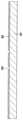
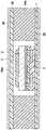
도 1은 본 발명의 제 1 실시형태로서의 반도체 장치의 단면도를 나타낸다. 이 반도체 장치는 에폭시계 수지, 폴리이미드계 수지, 유리포기재 에폭시수지 등으로 이루어지는 평면 방형 형상의 하층 절연막(1)을 구비하고 있다. 하층 절연막 (1)의 상면 중앙부에는 반도체 구성체(2)가 에폭시계 수지 등으로 이루어지는 접착층(3)을 통해 탑재되어 있다.1 shows a cross-sectional view of a semiconductor device as a first embodiment of the present invention. This semiconductor device is provided with the planar square lower
반도체 구성체(2)는 평면 방형 형상의 실리콘 기판(반도체 기판)(4)을 구비하고 있다. 실리콘 기판(4)의 하면에는 소정의 기능의 집적회로(도시하지 않음)가 설치되고, 하면 주변부에는 집적회로에 접속된, 알루미늄계 금속 등으로 이루어지는 복수의 접속패드(5)가 실리콘 기판의 변을 따라 설치되어 있다. 접속패드(5)의 중앙부를 제외한 실리콘 기판(4)의 하면에는 산화 실리콘 등으로 이루어지는 절연막(6)이 설치되고, 접속패드(5)의 중앙부는 절연막(6)에 설치된 개구부(7)를 통해 노출되어 있다.The
절연막(6)의 하면에는 폴리이미드계 수지 등으로 이루어지는 보호막(8)이 설치되어 있다. 절연막(6)의 개구부(7)에 대응하는 부분에 있어서의 보호막(8)에는 개구부(9)가 설치되어 있다. 보호막(8)의 하면에는 배선(배선 부재)(10)이 설치되어 있다. 배선(10)은 보호막(8)의 하면에 설치된 니켈로 이루어지는 밑바탕 금속층(11)과, 밑바탕 금속층(11)의 하면에 설치된 동(銅)으로 이루어지는 상부 금속층 (12)의 2층 구조로 되어 있다. 배선(10)의 일단부는 절연막(6) 및 보호막(8)의 개구부(7, 9)를 통해 접속패드(5)에 접속되어 있다. 배선(10)은 도면에서는 2개 만이 도시되어 있지만, 실제로는 평면 방형 형상의 실리콘 기판(4)의 각 변을 따라서 배열된 접속패드(5)에 대응하는 개수를 구비하고, 이후 설명하는 접속 패드부(외부 접속용 전극)(10a)로 된 각 타단부는 절연막(6) 아래에 있어서, 매트릭스 형상으로 배열되어 있다.On the lower surface of the insulating
그리고, 반도체 구성체(2)는 그 배선(10)을 포함하는 보호막(8)의 하면이 에폭시계 수지 등으로 이루어지는 접착층(3)을 통해 하층 절연막(1)의 상면 중앙부에 접착되어 있는 것에 의해, 하층 절연막(1)의 상면 중앙부에 탑재되어 있다. 반도체 구성체(2)의 배선(10)의 접속 패드부(외부 접속용 전극)(10a)의 하면 중앙부에 대응하는 부분에 있어서의 하층 절연막(1) 및 접착층(절연막)(3)에는 평면 형상이 원형인 개구부(접속용 개구부)(13)가 설치되어 있다.And the
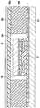
하층 절연막(1)의 하면에는 하층 배선(배선)(21)이 설치되어 있다. 하층 배선(21)은 하층 절연막(1)의 하면에 설치된 니켈로 이루어지는 밑바탕 금속층(22)과, 밑바탕 금속층(22)의 하면에 설치된 동으로 이루어지는 상부 금속층(23)의 2층 구조로 되어 있다. 하층 배선(21)의 일단부는 하층 절연막(1) 및 접착층(3)의 개구부(13)를 통해 반도체 구성체(2)의 배선(10)의 접속 패드부(10a)에 접속되어 있다.The lower layer wiring (wiring) 21 is provided on the lower surface of the lower
하층 배선(21) 및 하층 절연막(1)의 하면에는 솔더 레지스트 등으로 이루어지는 하층 오버코트막(31)이 설치되어 있다. 하층 배선(21)의 접속 패드부에 대응하는 부분에 있어서의 하층 오버코트막(31)에는 개구부(32)가 설치되어 있다. 하층 오버코트막(31)의 개구부(32)내 및 그 하부에는 땜납볼(33)이 하층 배선(21)의 접속 패드부에 접속되어서 설치되어 있다.On the lower surfaces of the
반도체 구성체(2) 및 접착층(3)의 주위에 있어서, 하층 절연막(1)의 상면에는 절연층(34)이 설치되어 있다. 절연층(34)은 에폭시계 수지, 폴리이미드계 수지, 유리포기재 에폭시수지 등으로 이루어져 있다. 반도체 구성체(2) 및 절연층 (34)의 상면에는 하층 절연막(1)과 동일한 재료로 이루어지는 상층 절연막(35)이 설치되어 있다.In the circumference | surroundings of the
상층 절연막(35)의 상면에는 상층 배선(36)이 설치되어 있다. 상층 배선 (36)은 상층 절연막(35)의 상면에 설치된 니켈로 이루어지는 밑바탕 금속층(37)과, 밑바탕 금속층(37)의 상면에 설치된 동으로 이루어지는 상부 금속층(38)의 2층 구조로 되어 있다. 상층 배선(36) 및 상층 절연막(35)의 상면에는 솔더 레지스트 등으로 이루어지는 상층 오버코트막(39)이 설치되어 있다. 상층 배선(36)의 접속 패드부에 대응하는 부분에 있어서의 상층 오버코트막(39)에는 개구부(40)가 설치되어 있다.The
하층 배선(21)과 상층 배선(36)은 하층 절연막(1), 절연층(34) 및 상층 절연막(35)에 설치된 관통구멍(41)의 내벽면에 설치된 상하 도통부(42)를 통해 접속되어 있다. 상하 도통부(42)는 관통구멍(41)의 내벽면에 설치된 니켈로 이루어지는 밑바탕 금속층(43)과, 밑바탕 금속층(43)의 내면에 설치된 동으로 이루어지는 상부 금속층(44)의 2층 구조로 되어 있다. 상하 도통부(42)내에는 솔더 레지스트 등으로 이루어지는 충전재(45)가 충전되어 있다.The
다음에, 이 반도체 장치의 제조방법의 일례에 대해 설명한다. 우선, 도 2에 나타내는 바와 같이, 동박으로 이루어지는 베이스판(51)의 상면에 무전해 니켈도금으로 이루어지는 마스크 금속층(52)이 형성된 것을 준비한다. 이 경우, 이 준비했던 것의 사이즈는, 도 1에 나타내는 완성된 반도체 장치를 복수개 형성하는 것이 가능한 사이즈로 되어 있다. 마스크 금속층(52)은 후술하는 레이저 빔을 조사해 서, 레이저 가공할 때에 사용하는 마스크를 형성하기 위한 것이다.Next, an example of the manufacturing method of this semiconductor device is demonstrated. First, as shown in FIG. 2, the
다음에, 도 3a 및 도 3a의 평면도인 도 3b에 나타내는 바와 같이, 포토 리소그래피법에 의해, 마스크 금속층(52)의 소정의 개소(도 1에 나타내는 반도체 구성체(2)의 배선(10)의 접속 패드부(10a)의 하면 중앙부에 대응하는 부분)에 평면 형상이 원형인 개구부(53)를 형성한다. 다음에, 도 4에 나타내는 바와 같이, 개구부 (53)내를 포함하는 마스크 금속층(52)의 상면에 에폭시계 수지, 폴리이미드계 수지, 유리포기재 에폭시수지 등으로 이루어지는 하층 절연막(1)을 형성한다.Next, as shown in FIG. 3B which is the top view of FIGS. 3A and 3A, the connection of the
다음에, 도 5에 나타내는 바와 같이, 반도체 구성체(2)를 준비한다. 상기 반도체 구성체(2)는 웨이퍼 상태의 실리콘 기판(4) 아래에 집적회로(도시하지 않음), 알루미늄계 금속 등으로 이루어지는 접속패드(5), 산화 실리콘 등으로 이루어지는 절연막(6), 폴리이미드계 수지 등으로 이루어지는 보호막(8) 및 배선(10)(니켈로 이루어지는 밑바탕 금속층(11) 및 동으로 이루어지는 상부 금속층(12))을 형성한 후, 다이싱에 의해 개편(個片)화하는 것으로 얻어진다.Next, as shown in FIG. 5, the
다음에, 하층 절연막(1)의 상면의 반도체 구성체 탑재영역에 반도체 구성체(2)의 배선(10)을 포함하는 보호막(8)의 하면을 에폭시계 수지 등으로 이루어지는 접착층(3)을 통해 접착함으로써, 반도체 구성체(2)를 탑재한다. 이 경우, 하층 절연막(1)의 상면의 반도체 구성체 탑재영역에 NCP(Non-Conductive Paste)라고 일컬어지는 접착재를 인쇄법이나 디스팬서 등을 이용하거나, 또는 NCF(Non-Conductive Film)라고 일컬어지는 접착 시트를 미리 공급해 두고, 가열 압착에 의해서 반도체 구성체(2)를 하층 절연막(1)의 상면에 고착한다.Next, the lower surface of the
다음에, 도 6에 나타내는 바와 같이, 접착층(3)을 포함하는 반도체 구성체 (2)의 주위에 있어서의 하층 절연막(1)의 상면에 격자 형상의 절연층 형성용 시트 (34a)를 핀 등으로 위치 결정하면서 배치한다. 절연층 형성용 시트(34a)는 예를 들면, 유리포 등으로 이루어지는 기재에 에폭시계 수지 등으로 이루어지는 열경화성 수지를 함침시키고, 열경화성 수지를 반경화 상태로 해서 시트 형상으로 이루며, 펀칭 등에 의해 복수의 사각형 형상의 개구부(54)를 형성한 것이다. 절연층 형성용 시트(34a)의 개구부(54)의 사이즈는 반도체 구성체(2)의 사이즈보다 약간 크게 되어 있다. 이 때문에, 절연층 형성용 시트(34a)와 반도체 구성체(2)의 사이에는 간극(55)이 형성되어 있다.Next, as shown in FIG. 6, the lattice-shaped insulating
다음에, 절연층 형성용 시트(34a)의 상면에 동박으로 이루어지는 서브 베이스판(56)의 하면에 상층 절연막 형성용층(35a)이 형성된 것을 배치한다. 상층 절연막 형성용층(35a)은 하층 절연막(1)과 동일한 재료로 이루어지고, 그 중의 에폭시계 수지 등으로 이루어지는 열경화성 수지는 반경화 상태로 되어 있다.Next, an upper insulating
다음에, 도 7에 나타내는 바와 같이, 한 쌍의 가열 가압판(57, 58)을 이용해서, 상하로부터 절연층 형성용 시트(34a) 및 상층 절연막 형성용층(35a)을 가열 가압한다. 이 가열 가압에 의해, 절연층 형성용 시트(34a) 및 상층 절연막 형성용층 (35a)중의 열경화성 수지가 유동해서, 도 8에 나타내는 간극(55)에 충전되고, 그 후의 냉각에 의해 고체화됨에 따라, 접착층(3)을 포함하는 반도체 구성체(2)의 주위에 있어서의 하층 절연막(1)의 상면에 절연층(34)이 형성되며, 또한 반도체 구성체(2) 및 절연층(34)의 상면에 상층 절연막(35)이 형성된다.Next, as shown in FIG. 7, the insulating
여기서, 도 6에 나타내는 바와 같이, 절연층 형성용 시트(34a)의 하면에는 하층 절연막(1) 및 베이스판(51)이 배치되고, 절연층 형성용 시트(34a)의 상면에는 하층 절연막(1)과 동일한 재료로 이루어지는 상층 절연막 형성용층(35a) 및 베이스판(51)과 동일한 재료로 이루어지는 서브 베이스판(56)이 배치되어 있으므로, 절연층 형성용 시트(34a)의 부분에 있어서의 두께 방향의 재료 구성이 대칭으로 된다. 이 결과, 가열 가압에 의해, 절연층 형성용 시트(34a) 및 상층 절연막 형성용층 (35a)이 대칭적으로 경화되고, 두께 방향으로 수축되며, 나아가서는 전체로서 휘어진 상태가 발생하기 어려우며, 그 이후의 공정에의 반송이나 그 이후의 공정에서의 가공 정밀도에 지장을 초래하기 어렵게 할 수 있다.6, the lower insulating
이 경우, 하층 절연막(1)은 그 중의 열경화성 수지가 미리 경화되어 있기 때문에, 가열 가압되어도 거의 변형되지 않는다. 또, 서브 베이스판(56)에 의해, 상측의 가열 가압판(57)의 하면에 상층 절연막 형성용층(35a)중의 열경화성 수지가 불필요하게 부착되는 것을 방지할 수 있다. 이 결과, 상측의 가열 가압판(57)을 그대로 재사용할 수 있다.In this case, the lower insulating
다음에, 베이스판(51) 및 서브 베이스판(56)을 에칭에 의해서 제거하면, 도 8에 나타내는 바와 같이, 개구부(53)내에 충전된 하층 절연막(1)을 포함하는 마스크 금속층(52)의 하면이 노출되고, 또한 상층 절연막(35)의 상면이 노출된다. 이 상태에서는 베이스판(51) 및 서브 베이스판(56)을 제거해도, 하층 절연막(1), 절연층(34) 및 상층 절연막(35)의 존재에 의해, 강도를 충분하게 확보할 수 있다. 이와 같이, 본 실시형태에서는 제조 공정중에 필요하게 되는 베이스판(51) 및 서브 베이스판(56)을 에칭에 의해서 제거하므로, 완성되는 반도체 장치의 두께를 얇게 할 수 있다고 하는 효과를 갖는다.Next, when the
다음에, 도 9에 나타내는 바와 같이, 레이저 빔의 조사에 의한 레이저 가공에 의해서, 마스크 금속층(52)의 개구부(53)내의 하층 절연막(1)을 제거하는 동시에, 반도체 구성체(2)의 배선(10)의 접속 패드부(10a)의 하면 중앙부에 대응하는 부분에 있어서의 하층 절연막(1) 및 접착층(3)에 개구부(13)를 형성한다. 또, 하층 절연막(1), 절연층(34) 및 상층 절연막(35)에 메카니컬 드릴(Mechanical Drill)을 이용하거나 또는 레이저 빔의 조사에 의한 레이저 가공에 의해서, 관통구멍(41)을 형성한다.Next, as shown in FIG. 9, the lower insulating
레이저 빔을 조사해서 개구부(13)를 형성하는 경우에 대해 설명한다. 레이저 빔을 하층 절연막(1) 및 접착층(3)에 직접 조사하면, 그 빔의 직경에 따른 직경의 개구부가 형성된다. 여기서, 마스크 금속층(52)의 개구부(53)의 직경은 반도체 구성체(2)의 배선(10)의 접속 패드부(10a)의 직경보다 작아져 있다. 이 때문에, 레이저 빔의 빔의 직경이 반도체 구성체(2)의 배선(10)의 접속 패드부(10a)의 직경보다 크면, 마스크 금속층(52)의 개구부(53)의 외부로 조사되는 레이저 빔은 마스크 금속층(52)에 의해서 차단되기 때문에, 하층 절연막(1) 및 접착층(3)에 형성되는 개구부(13)의 직경은 마스크 금속층(52)의 개구부(53)의 직경에 따른 크기로 된다.The case where the
즉, 마스크 금속층(52)은 개구부(53)를 갖는 것에 의해, 레이저 빔의 조사에 의한 레이저 가공에 의해서 하층 절연막(1) 및 접착층(3)에 개구부(13)를 형성할 때의 마스크로서 기능하고, 하층 절연막(1) 및 접착층(3)에 마스크 금속층(52)의 개구부(53)에 셀프 얼라인먼트되어, 금속층(52)의 개구부(53)와 동일한 직경의 개구부(13)가 형성된다. 또한, 개구부(13)는 그 평면 형상이 원형에 한정되는 것이 아니고, 마스크 금속층(52)의 개구부(53)를 바꿈으로써, 여러 가지의 형상으로 하는 것이 가능하며, 요점은 개구부(13)의 평면 형상이 접속 패드부(10a)의 평면 사이즈보다 작은 것으로 하면 좋다.That is, since the
이 결과, 하층 절연막(1) 및 접착층(3)에 형성해야 할 개구부(13)의 직경을 가급적으로 작게 하는 것이 가능해지고, 또한 마스크 금속층(52)에 대한 반도체 구성체(2)의 배선(10)의 접속 패드부(10a)의 위치 맞춤이 비교적 용이해지며, 나아가서는 반도체 구성체(2)의 배선(10)의 접속 패드부(10a)의 직경을 가급적으로 작게 하는 것이 가능해지고, 반도체 구성체(2)의 미세화가 가능해진다.As a result, the diameters of the
예를 들면, 현상에서는 레이저 빔의 빔의 직경이 최소인 50μm정도이고, 하층 절연막(1) 및 접착층(3)에 직접 조사하면, 그들 형성되는 개구부의 직경은 70μm정도로 된다. 이 때문에, 조사되는 레이저 빔을 전부 수광하려면, 반도체 구성체(2)의 배선(10)의 접속 패드부(10a)의 직경은 레이저 가공 정밀도를 고려하면, 현상의 방법에서는 100∼120μm로 할 필요가 있다.For example, in development, the diameter of the beam of a laser beam is about 50 micrometers which is minimum, and when the lower insulating
이것에 대해, 마스크 금속층(52)을 레이저 빔의 마스크로 하는 본 실시형태의 방법에서는 포토 리소그래피법에 의해 형성되는 마스크 금속층(52)의 개구부 (53)의 직경은 20∼50μm, 특히, 20∼30μm로 하는 것이 가능하므로, 반도체 구성체(2)의 배선(10)의 접속 패드부(10a)의 직경은 50∼80μm, 특히, 50∼60μm로 하 는 것이 가능해짐에 따라, 반도체 구성체(2)의 미세화가 가능해진다.On the other hand, in the method of this embodiment which uses the
다음에, 마스크 금속층(52)을 에칭에 의해 제거하면, 도 10에 나타내는 바와 같이, 하층 절연막(1)의 하면이 노출된다. 이와 같이, 본 실시형태에서는 제조공정중에 필요하게 되는 마스크 금속층(52)을 에칭에 의해서 제거하므로, 완성되는 반도체 장치의 두께를 얇게 할 수 있다고 하는 효과를 갖는다.Next, when the
다음에, 도 11에 나타내는 바와 같이, 하층 절연막(1) 및 접착층(3)의 개구부(13)를 통해 노출된 반도체 구성체(2)의 배선(10)의 접속 패드부(10a)의 하면을 포함하는 하층 절연막(1)의 하면 전체, 상층 절연막(35)의 상면 전체 및 관통구멍 (41)의 내벽면에 니켈의 무전해도금에 의해서, 밑바탕 금속층(22, 37, 43)을 형성한다. 다음에, 밑바탕 금속층(22, 37, 43)을 도금 전류로서 동의 전해도금을 실행함으로써, 밑바탕 금속층(22, 37, 43)의 표면에 상부 금속층(23, 38, 44)을 형성한다.Next, as shown in FIG. 11, the lower surface of the
다음에, 상부 금속층(23, 38) 및 밑바탕 금속층(22, 37)을 포토 리소그래피법에 의해서 패터닝하면, 도 12에 나타내는 바와 같이 된다. 즉, 하층 절연막(1)의 하면에 밑바탕 금속층(22) 및 상부 금속층(23)으로 이루어지는 2층 구조의 하층 배선(21)이 형성된다. 또, 상층 절연막(35)의 상면에 밑바탕 금속층(37) 및 상부 금속층(38)으로 이루어지는 2층 구조의 상층 배선(36)이 형성된다. 또한, 관통구멍(41)의 내벽면에 밑바탕 금속층(43) 및 상부 금속층(44)으로 이루어지는 2층 구조의 상하 도통부(42)가 형성된다. 또한, 하층 배선(21), 상층 배선(36) 및 상하 도통부(42)는 밑바탕 금속층(22, 37) 위에 상부 금속층 형성영역이 제거된 도금 레 지스트막을 형성한 후, 전해도금에 의해 상부 금속층(23, 28, 44)을 형성하는 패턴 도금법에 의해서 형성해도 좋다. 또한, 각 도면에서 개구부(13)내에는 도시의 형편상, 밑바탕 금속층(22)만이 형성되어 있지만, 개구부(13)내에는 밑바탕 금속층 (22)과 함께 상부 금속층(23)을 형성하는 것도 가능하다.Next, when the upper metal layers 23 and 38 and the
다음에, 도 13에 나타내는 바와 같이, 하층 배선(21)을 포함하는 하층 절연막(1)의 하면에 스크린 인쇄법, 스핀코트법 등에 의해서, 솔더 레지스트 등으로 이루어지는 하층 오버코트막(31)을 형성한다. 또, 상층 배선(36)을 포함하는 상층 절연막(35)의 상면에 스크린 인쇄법, 스핀코트법 등에 의해서, 솔더 레지스트 등으로 이루어지는 상층 오버코트막(39)을 형성한다. 이 상태에서는 상하 도통부(42)내에 솔더 레지스트 등으로 이루어지는 충전재(45)가 충전되어 있다.Next, as shown in FIG. 13, the lower
다음에, 하층 배선(21)의 접속 패드부에 대응하는 부분에 있어서의 하층 오버코트막(31)에 레이저 빔의 조사에 의한 레이저 가공에 의해서, 개구부(32)를 형성한다. 또, 상층 배선(36)의 접속 패드부에 대응하는 부분에 있어서의 상층 오버코트막(39)에 레이저 빔의 조사에 의한 레이저 가공에 의해서, 개구부(40)를 형성한다.Next, the opening
다음에, 하층 오버코트막(31)의 개구부(32)내 및 그 하부에 땜납볼(33)을 하층 배선(21)의 접속 패드부에 접속시켜서 형성한다. 다음에, 서로 인접하는 반도체 구성체(2) 사이에 있어서, 하층 오버코트막(31), 하층 절연막(1), 절연층(34), 상층 절연막(35) 및 상층 오버코트막(39)을 절단하면, 도 1에 나타내는 반도체 장치가 복수개 얻어진다.Next, the
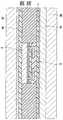
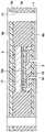
(제 2 실시형태)(2nd embodiment)
도 14는 본 발명의 제 2 실시형태로서의 반도체 장치의 단면도를 나타낸다. 이 반도체 장치에 있어서, 도 1에 나타내는 반도체 장치와 다른 점은 하층 배선 (21)과 하층 절연막(1)의 사이에 동으로 이루어지는 하부 금속층(61)을 설치하고, 상층 배선(36)과 상층 절연막(35)의 사이에 동으로 이루어지는 하부 금속층(62)을 설치하며, 반도체 구성체(2)의 실리콘 기판(4)의 상면을 에폭시계 수지 등으로 이루어지는 접착층(63)을 통해 상층 절연막(35)의 하면에 접착한 점이다. 이 경우, 하층 배선(21)의 일단부는 하부 금속층(61)의 개구부(64)와 하층 절연막(1) 및 접착층(3)의 개구부(13)를 통해 반도체 구성체(2)의 배선(10)의 접속 패드부(10a)에 접속되어 있다.14 is a sectional view of a semiconductor device as a second embodiment of the present invention. This semiconductor device differs from the semiconductor device shown in FIG. 1 by providing a
다음에, 이 반도체 장치의 제조방법의 일례에 대해 설명한다. 우선, 도 15에 나타내는 바와 같이, 에폭시계 수지, 폴리이미드계 수지, 유리포기재 에폭시수지 등의 시트로 이루어지는 하층 절연막(1)의 하면에 동박으로 이루어지는 형상의 마스크 금속층(65)이 고착된 적층 시트를 준비한다. 이 경우도, 이 준비한 것의 사이즈는 도 14에 나타내는 완성된 반도체 장치를 복수개 형성하는 것이 가능한 사이즈로 되어 있다.Next, an example of the manufacturing method of this semiconductor device is demonstrated. First, as shown in FIG. 15, the lamination | stacking which the
다음에, 도 16에 나타내는 바와 같이, 포토 리소그래피법에 의해서, 마스크 금속층(65)의 소정의 개소(도 14에 나타내는 반도체 구성체(2)의 배선(10)의 접속 패드부(10a)의 하면 중앙부에 대응하는 부분)에 평면 형상이 원형인 개구부(64)를 형성한다.Next, as shown in FIG. 16, the center part of the lower surface of the
다음에, 도 17에 나타내는 바와 같이, 하층 절연막(1)의 상면의 반도체 구성체 탑재영역에 반도체 구성체(2)의 배선(10)을 포함하는 보호막(8)의 하면을 에폭시계 수지 등으로 이루어지는 접착층(3)을 통해 접착함으로써, 반도체 구성체(2)를 탑재한다. 이 경우도, NCP라고 일컬어지는 접착재 또는 NCF라고 일컬어지는 접착 시트를 하층 절연막(1)의 상면의 반도체 구성체 탑재영역에 미리 공급해 두고, 가열 압착에 의해서 반도체 구성체(2)를 하층 절연막(1)의 상면에 고착한다.Next, as shown in FIG. 17, the lower surface of the
다음에, 도 18에 나타내는 바와 같이, 접착층(3)을 포함하는 반도체 구성체 (2)의 주위에 있어서의 하층 절연막(1)의 상면에 격자 형상의 절연층 형성용 시트(34a)를 핀 등으로 위치 결정하면서 배치한다. 다음에, 반도체 구성체(2)의 실리콘 기판(4)의 상면에 디스팬서 등을 이용해서, 실리콘 커플링제를 포함하는 에폭시계 수지 등으로 이루어지는 액상의 접착재(62a)를 도포한다. 다음에, 절연층 형성용 시트(34a)의 상면에 동박으로 이루어지는 서브 베이스판(56)의 하면에 상층 절연막(35)이 형성된 것을 배치한다. 이 경우, 상층 절연막(35)중의 에폭시계 수지 등으로 이루어지는 열경화성 수지는 이미 경화되어 있다.Next, as shown in FIG. 18, the lattice-shaped insulating
다음에, 도 19에 나타내는 바와 같이, 한 쌍의 가열 가압판(57, 58)을 이용해서 상하로부터 가열 가압하면, 접착층(3)을 포함하는 반도체 구성체(2)의 주위에 있어서의 하층 절연막(1)의 상면에 절연층(34)이 형성되고, 상층 절연막(35)의 하면에 반도체 구성체(2)의 실리콘 기판(4)의 상면이 접착층(63)을 통해 접착된 후, 절연층(34)의 상면에 상층 절연막(35)의 하면이 고착된다.Next, as shown in FIG. 19, when heat-pressurizing from the upper and lower sides using the pair of
다음에, 도 20에 나타내는 바와 같이, 레이저 빔의 조사에 의한 레이저 가공 에 의해서, 개구부(64)를 갖는 마스크 금속층(65)을 마스크로서, 반도체 구성체(2)의 배선(10)의 접속 패드부(10a)의 하면 중앙부에 대응하는 부분에 있어서의 하층 절연막(1) 및 접착층(3)에 개구부(13)를 형성한다. 또, 마스크 금속층(65), 하층 절연막(1), 절연층(34), 상층 절연막(35) 및 서브 베이스판(56)의 소정의 개소에 메카니컬 드릴을 이용하거나 또는 레이저 빔의 조사에 의한 레이저 가공에 의해서 관통구멍(41)을 형성한다.Next, as shown in FIG. 20, the connection pad part of the
다음에, 도 21에 나타내는 바와 같이, 마스크 금속층(65)의 개구부(64)와 하층 절연막(1) 및 접착층(3)의 개구부(13)를 통해 노출된 반도체 구성체(2)의 배선(10)의 접속 패드부(10a)의 하면을 포함하는 마스크 금속층(65)의 하면 전체, 서브 베이스판(56)의 상면 전체 및 관통구멍(41)의 내벽면에 니켈의 무전해도금에 의해서, 밑바탕 금속층(22, 37, 43)을 형성한다. 다음에, 밑바탕 금속층(22, 37, 43)을 도금 전류로로서 동의 전해도금을 실행함으로써, 밑바탕 금속층(22, 37, 43)의 표면에 상부 금속층(23, 38, 44)을 형성한다.Next, as shown in FIG. 21, the
다음에, 포토 리소그래피법에 의해서, 상부 금속층(23), 밑바탕 금속층(22) 및 마스크 금속층(65)을 패터닝하고, 또한 상부 금속층(38), 밑바탕 금속층(37) 및 서브 베이스판(56)을 패터닝하면, 도 22에 나타내는 바와 같이 된다. 즉, 하층 절연막(1)의 하면에 하부 금속층(61)을 갖고, 해당 하부 금속층(61)과 동일한 평면 형상을 갖는 밑바탕 금속층(22) 및 상부 금속층(23)으로 이루어지는 2층 구조의 하층 배선(21)이 형성된다. 또, 상층 절연막(35)의 상면에 하부 금속층(62)을 갖는 밑바탕 금속층(37) 및 상부 금속층(38)으로 이루어지는 2층 구조의 상층 배선(36) 이 형성된다. 또한, 관통구멍(41)의 내벽면에 밑바탕 금속층(43) 및 상부 금속층 (44)으로 이루어지는 2층 구조의 상하 도통부(42)가 형성된다. 이하, 상기 제 1 실시형태의 경우와 똑같은 공정을 거치면, 도 13에 나타내는 반도체 장치가 복수개 얻어진다.Next, the
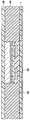
(제 3 실시형태)(Third embodiment)
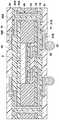
도 23은 본 발명의 제 3 실시형태로서의 반도체 장치의 단면도를 나타낸다. 이 반도체 장치에 있어서, 도 1에 나타내는 반도체 장치와 크게 다른 점은 빌드업 공법에 의해서, 하층 배선 및 상층 배선을 모두 2층 배선 구조로 한 점이다. 즉, 제 1 하층 배선(21A) 및 하층 배선(21)을 포함하는 제 1 하층 절연막(1A)의 하면에는 제 1 하층 절연막(1A)과 동일한 재료로 이루어지는 제 2 하층 절연막(1B)이 설치되어 있다.Fig. 23 is a sectional view of a semiconductor device as a third embodiment of the present invention. In this semiconductor device, the difference from the semiconductor device shown in FIG. 1 is that the lower layer wiring and the upper layer wiring are both two-layer wiring structures by the build-up method. That is, the second lower
제 2 하층 절연막(1B)의 하면에 설치된 제 2 하층 배선(21B)의 일단부는 제 2 하층 절연막(1B)에 설치된 개구부(71)를 통해, 제 1 하층 배선(21A)의 접속 패드부에 접속되어 있다. 제 2 하층 배선(21B)을 포함하는 제 2 하층 절연막(1B)의 하면에는 하층 오버코트막(31)이 설치되어 있다. 하층 오버코트막(31)의 개구부(32)내 및 그 하부에는 땜납볼(33)이 제 2 하층 배선(21B)의 접속 패드부에 접속되어서 설치되어 있다.One end of the second
제 1 상층 배선(36A)을 포함하는 제 1 상층 절연막(35A)의 상면에는 제 1 상층 절연막(35A)과 동일한 재료로 이루어지는 제 2 상층 절연막(35B)이 설치되어 있다. 제 2 상층 절연막(35B)의 상면에 설치된 제 2 상층 배선(36B)의 일단부는 제 2 상층 절연막(35B)에 설치된 개구부(72)를 통해, 제 1 상층 배선(36A)의 접속 패드부에 접속되어 있다. 제 2 상층 배선(36B)을 포함하는 제 2 상층 절연막(35B)의 상면에는 상층 오버코트막(39)이 설치되어 있다. 제 2 상층 배선(36B)의 접속 패드부에 대응하는 부분에 있어서의 상층 오버코트막(39)에는 개구부(40)가 설치되어 있다. 또한, 하층 배선 및 상층 배선은 모두 3층 이상의 배선 구조로 해도 좋다.On the upper surface of the first upper insulating
(제 4 실시형태)(4th Embodiment)
도 24는 본 발명의 제 4 실시형태로서의 반도체 장치의 단면도를 나타낸다. 이 반도체 장치에 있어서, 도 1에 나타내는 반도체 장치와 크게 다른 점은 상하 도통부(42)를 구비하고 있지 않고, 그 대신에 접착층(3)을 포함하는 반도체 구성체 (2)의 주위에 있어서의 절연층(34)중에 사각형 프레임 형상으로 양면 배선 구조의 회로기판(81)을 매립해서 배치한 점이다.24 is a sectional view of a semiconductor device as a fourth embodiment of the present invention. This semiconductor device differs greatly from the semiconductor device shown in FIG. 1 in that it is not provided with the upper and lower
이 경우, 회로기판(81)은 유리포기재 에폭시수지 등으로 이루어지는 사각형 프레임 형상의 기판(82)을 구비하고 있다. 기판(82)의 하면에는 동박으로 이루어지는 하층 배선(83)이 설치되고, 상면에는 동박으로 이루어지는 상층 배선(84)이 설치되어 있다. 하층 배선(83)과 상층 배선(84)은 기판(82)의 내부에 설치된 도전성 페이스트 등으로 이루어지는 상하 도통부(85)를 통해 접속되어 있다.In this case, the
하층 배선(21)은 하층 절연막(1) 및 절연층(34)에 설치된 개구부(86)를 통해 회로기판(81)의 하층 배선(83)의 접속 패드부에 접속되어 있다. 상층 배선(36)은 상층 절연막(35) 및 절연층(34)에 설치된 개구부(87)를 통해 회로기판(81)의 상층 배선(84)의 접속 패드부에 접속되어 있다.The
다음에, 이 반도체 장치의 제조방법의 일례에 대해 설명한다. 이 경우, 도 6에 나타내는 공정에 있어서, 도 25에 나타내는 바와 같이, 접착층(3)을 포함하는 반도체 구성체(2)의 주위에 있어서의 하층 절연막(1)의 상면에 격자 형상의 절연층 형성용 시트(34a), 격자 형상의 회로기판(81) 및 격자 형상의 절연층 형성용 시트 (34a)를 핀 등으로 위치 결정하면서 배치한다. 다음에, 상측의 절연층 형성용 시트(34a)의 상면에, 서브 베이스판(56)의 하면에 상층 절연막 형성용층(35a)이 형성된 것을 배치한다. 이 경우, 반도체 구성체(2)의 배선(10)의 접속 패드부(10a)의 하면 중앙부 및 회로기판(81)의 하층 배선(83)의 접속 패드부의 하면 중앙부에 대응하는 부분에 있어서의 마스크 금속층(52)에는 개구부(53a, 53b)가 형성되어 있다.Next, an example of the manufacturing method of this semiconductor device is demonstrated. In this case, in the step shown in FIG. 6, as shown in FIG. 25, a lattice-shaped insulating layer is formed on the upper surface of the lower insulating
다음에, 도 26에 나타내는 바와 같이, 한 쌍의 가열 가압판(57, 58)을 이용해서 상하로부터 가열 가압하면, 접착층(3)을 포함하는 반도체 구성체(2)의 주위에 있어서의 하층 절연막(1)의 상면에 절연층(34)이 형성되고, 또한 절연층(34)중에 회로기판(81)이 매립되고, 반도체 구성체(2) 및 절연층(34)의 상면에 상층 절연막 (35)이 형성된다. 다음에, 베이스판(51) 및 서브 베이스판(56)을 에칭에 의해서 제거하면, 도 27에 나타내는 바와 같이, 마스크 금속층(52)의 개구부(53a, 53b)내에 충전된 하층 절연막(1)을 포함하는 마스크 금속층(52)의 하면이 노출되고, 또한 상층 절연막(35)의 상면이 노출된다.Next, as shown in FIG. 26, when it heat-presses from the top and bottom using a pair of
다음에, 도 28에 나타내는 바와 같이, 레이저 빔의 조사에 의한 레이저 가공에 의해서, 개구부(53a, 53b)를 갖는 마스크 금속층(52)을 마스크로서 반도체 구성 체(2)의 배선(10)의 접속 패드부(10a)의 하면 중앙부에 대응하는 부분에 있어서의 하층 절연막(1) 및 접착층(3)에 개구부(13)를 형성하고, 또한 회로기판(81)의 하층 배선(83)의 접속 패드부의 하면 중앙부에 대응하는 부분에 있어서의 하층 절연막 (1) 및 절연층(34)에 개구부(86)를 형성한다. 이 경우, 개구부(86)의 직경은 개구부(13)의 직경과 동일하게 된다.Next, as shown in FIG. 28, connection of the
또, 레이저 빔의 조사에 의한 레이저 가공에 의해서, 회로기판(81)의 상층 배선(84)의 접속 패드부에 대응하는 부분에 있어서의 상층 절연막(35) 및 절연층 (34)에 개구부(87)를 형성한다. 이 경우, 개구부(87)의 직경은 개구부(13)의 직경보다 커진다. 이하, 상기 제 1 실시형태의 경우와 똑같은 공정을 거치면, 도 24에 나타내는 반도체 장치가 복수개 얻어진다.Moreover, the opening
이와 같이 해서 얻어진 반도체 장치에서는 도 24에 나타내는 반도체 장치에 비해, 하층 배선 및 상층 배선을 2층 구조로 해도 하층 절연막 및 상층 절연막이 1층이므로, 그만큼 박형화할 수 있다. 또, 상하 도통부(42)를 구비하고 있지 않으므로, 메카니컬 드릴에 의한 관통구멍(41)의 형성을 실행할 필요는 없다.In the semiconductor device thus obtained, the lower layer insulating film and the upper layer insulating film have one layer, compared with the semiconductor device shown in Fig. 24, and thus the thickness of the lower insulating film and the upper insulating film is one. In addition, since the upper and lower
(제 5 실시형태)(Fifth Embodiment)
도 29는 본 발명의 제 5 실시형태로서의 반도체 장치의 단면도를 나타낸다. 이 반도체 장치에 있어서, 도 1에 나타내는 반도체 장치와 다른 점은 반도체 구성체(2)의 배선(10)을 포함하는 보호막(8)의 하면에 폴리이미드계 수지, 에폭시계 수지 등의 절연재로 이루어지는 정전기 방지용 보호막(91)을 설치한 점이다.29 is a sectional view of a semiconductor device as a fifth embodiment of the present invention. In this semiconductor device, the difference from the semiconductor device shown in FIG. 1 is that static electricity is formed on the lower surface of the
따라서, 이 경우, 반도체 구성체(2)의 정전기 방지용 보호막(91)의 하면은 접착층(3)을 통해 하층 절연막(1)의 상면 중앙부에 접착되어 있다. 하층 배선(21)은 하층 절연막(1), 접착층(3) 및 정전기 방지용 보호막(91)의 개구부(13)를 통해 반도체 구성체(2)의 배선(10)의 접속 패드부(10a)에 접속되어 있다.Therefore, in this case, the lower surface of the antistatic
그런데, 반도체 구성체(2)를 하층 절연막(1) 위에 탑재하기 전에 있어서는, 개구부(13)는 정전기 방지용 보호막(91)에 형성되어 있지 않다. 그리고, 개구부 (13)를 갖지 않는 정전기 방지용 보호막(91)은 그 자체가 웨이퍼 상태의 실리콘 기판(4) 아래에 형성된 시점으로부터 반도체 구성체(2)가 하층 절연막(1) 위에 탑재되는 시점까지에 있어서, 실리콘 기판(4) 아래에 형성된 집적회로를 정전기로부터 보호하는 것이다.By the way, before mounting the
(제 6 실시형태)(Sixth Embodiment)
도 30은 본 발명의 제 6 실시형태로서의 반도체 장치의 단면도를 나타낸다. 이 반도체 장치에 있어서, 도 1에 나타내는 반도체 장치와 다른 점은 반도체 구성체(2)의 배선(10)의 접속 패드부(10a) 하면에 전해 동 도금으로 이루어지는 보호 금속층(92)을 설치한 점이다. 이 경우, 보호 금속층(92)은 레이저 빔이 조사될 때에, 배선(10)의 접속 패드부(10a)를 보호하기 위한 것이다. 즉, 배선(10)을 5∼10μm의 두께로 형성하고, 레이저 빔에 의해서 에칭되는 양을 고려해서, 상기 배선 (10)의 접속 패드부(10a) 위에만 보호 금속층(92)을 수 μm의 두께로 형성해 두면, 반도체 구성체(2)의 박형화를 도모할 수 있다.30 is a sectional view of a semiconductor device as a sixth embodiment of the present invention. This semiconductor device differs from the semiconductor device shown in FIG. 1 in that a
(제 7 실시형태)(Seventh Embodiment)
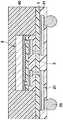
도 31은 본 발명의 제 7 실시형태로서의 반도체 장치의 단면도를 나타낸다. 이 반도체 장치에 있어서, 도 1에 나타내는 반도체 장치와 다른 점은 반도체 구성체(2)의 배선(10)의 접속 패드부(10a) 하면 중앙부에 전해 동 도금으로 이루어지는 기둥형상 전극(외부 접속용 전극)(93)을 설치하고, 배선(10)을 포함하는 보호막(8)의 하면 위에 에폭시계 수지 등으로 이루어지는 밀봉막(94)을, 그 하면이 기둥형상 전극(93)의 하면과 동일 평면으로 되도록 설치한 점이다. 이 경우, 기둥형상 전극 (93)을 포함하는 밀봉막(94)의 하면은 접착층(3)을 통해 하층 절연막(1)의 상면 중앙부에 접착되어 있다. 하층 배선(21)은 하층 절연막(1) 및 접착층(3)의 개구부 (13)를 통해 반도체 구성체(2)의 기둥형상 전극(93)에 접속되어 있다.31 is a sectional view of a semiconductor device as a seventh embodiment of the present invention. This semiconductor device differs from the semiconductor device shown in FIG. 1 in that the columnar electrode (electrode for external connection) is formed of electrolytic copper plating on the bottom surface of the
(제 8 실시형태)(8th Embodiment)
도 32는 본 발명의 제 8 실시형태로서의 반도체 장치의 단면도를 나타낸다. 이 반도체 장치에 있어서, 도 1에 나타내는 반도체 장치와 다른 점은 반도체 구성체(2) 및 하층 절연막(1)의 상면에 에폭시계 수지 등으로 이루어지는 밀봉막(절연층)(95)만을 설치한 점이다. 이 경우, 밀봉막(95)은 트랜스퍼 몰딩 등의 몰드법에 의해 형성된다.32 is a sectional view of a semiconductor device as an eighth embodiment of the present invention. This semiconductor device differs from the semiconductor device shown in FIG. 1 in that only the sealing film (insulation layer) 95 made of epoxy resin or the like is provided on the upper surface of the
또한, 상기 각 실시형태에 있어서, 마스크 금속층에 형성되는 개구부는 평면 형상이 원형으로 되는 것이었지만, 본 발명은 이것에 한정되는 것이 아니고, 평면 형상이 예를 들면, 다각형상의 것이든지, 임의의 형상으로 할 수 있는 것이다. 또, 하층 절연막에 레이저 빔을 조사해서 개구부를 형성할 때, 마스크 금속층은 개구부를 갖고 있어야만 하는 형상의 경우로 설명했지만, 하층 절연막에 레이저 빔을 조사하기 전에, 패터닝에 의해서 배선이나 패드부를 형성해 두어도 좋다. 또, 반 도체 구성체(2)에는 접속패드(5)에 접속된 배선(10)이 형성된 것으로 했지만, 본 발명은 배선의 드로잉부를 갖고 있지 않은 외부 접속용 전극만이 형성된 반도체 구성체에도 적용 가능하다. 그외, 본 발명의 취지에 따라, 여러 가지로 변형해서 적용하는 것이 가능하다.In addition, in each said embodiment, although the opening shape formed in the mask metal layer was a planar shape circular, this invention is not limited to this, The planar shape is polygonal or arbitrary shape, for example. You can do it. In the case where the opening is formed by irradiating a laser beam to the lower insulating film, the mask metal layer has been described as having a shape that must have an opening. However, even if the wiring and the pad portion are formed by patterning before irradiating the laser beam to the lower insulating film. good. Moreover, although the
도 1은 본 발명의 제 1 실시형태로서의 반도체 장치의 단면도이다.1 is a cross-sectional view of a semiconductor device as a first embodiment of the present invention.
도 2는 도 1에 나타내는 반도체 장치의 제조방법의 일례에 있어서, 당초 준비했던 것의 단면도이다.FIG. 2 is a cross-sectional view of one originally prepared in the method of manufacturing the semiconductor device shown in FIG. 1.
도 3a는 도 2에 연속되는 공정의 단면도, 도 3b는 그 평면도이다.3A is a sectional view of a process following FIG. 2, and FIG. 3B is a plan view thereof.
도 4는 도 3에 연속되는 공정의 단면도이다.4 is a cross-sectional view of the process following FIG. 3.
도 5는 도 4에 연속되는 공정의 단면도이다.FIG. 5 is a cross-sectional view of the process following FIG. 4.
도 6은 도 5에 연속되는 공정의 단면도이다.6 is a cross-sectional view of the process following FIG. 5.
도 7은 도 6에 연속되는 공정의 단면도이다.FIG. 7 is a cross-sectional view of the process following FIG. 6.
도 8은 도 7에 연속되는 공정의 단면도이다.8 is a cross-sectional view of the process following FIG. 7.
도 9는 도 8에 연속되는 공정의 단면도이다.9 is a cross-sectional view of the process following FIG. 8.
도 10은 도 9에 연속되는 공정의 단면도이다.10 is a cross-sectional view of the process following FIG. 9.
도 11은 도 10에 연속되는 공정의 단면도이다.FIG. 11 is a sectional view of a process following FIG. 10.
도 12는 도 11에 연속되는 공정의 단면도이다.12 is a sectional view of a process following FIG. 11.
도 13은 도 12에 연속되는 공정의 단면도이다.FIG. 13 is a sectional view of a process following FIG. 12.
도 14는 본 발명의 제 2 실시형태로서의 반도체 장치의 단면도이다.It is sectional drawing of the semiconductor device as 2nd Embodiment of this invention.
도 15는 도 14에 나타내는 반도체 장치의 제조방법의 일례에 있어서, 당초 준비했던 것의 단면도이다.FIG. 15 is a cross-sectional view of one originally prepared in the semiconductor device manufacturing method shown in FIG. 14.
도 16은 도 15에 연속되는 공정의 단면도이다.16 is a cross-sectional view of the process following FIG. 15.
도 17은 도 16에 연속되는 공정의 단면도이다.17 is a cross-sectional view of the process following FIG. 16.
도 18은 도 17에 연속되는 공정의 단면도이다.18 is a cross-sectional view of the process following FIG. 17.
도 19는 도 18에 연속되는 공정의 단면도이다.19 is a sectional view of a process following FIG. 18.
도 20은 도 19에 연속되는 공정의 단면도이다.20 is a cross-sectional view of the process following FIG. 19.
도 21은 도 20에 연속되는 공정의 단면도이다.21 is a sectional view of a process following FIG. 20.
도 22는 도 21에 연속되는 공정의 단면도이다.22 is a cross-sectional view of the process following FIG. 21.
도 23은 본 발명의 제 3 실시형태로서의 반도체 장치의 단면도이다.It is sectional drawing of the semiconductor device as 3rd Embodiment of this invention.
도 24는 본 발명의 제 4 실시형태로서의 반도체 장치의 단면도이다.24 is a cross-sectional view of a semiconductor device as a fourth embodiment of the present invention.
도 25는 도 24에 나타내는 반도체 장치의 제조방법의 일례에 있어서, 소정의 공정의 단면도이다.25 is a cross-sectional view of a predetermined step in one example of a method of manufacturing the semiconductor device shown in FIG. 24.
도 26은 도 25에 연속되는 공정의 단면도이다.FIG. 26 is a sectional view of a process following FIG. 25.
도 27은 도 26에 연속되는 공정의 단면도이다.FIG. 27 is a sectional view of a process following FIG. 26.
도 28은 도 27에 연속되는 공정의 단면도이다.FIG. 28 is a sectional view of a process following FIG. 27.
도 29는 본 발명의 제 5 실시형태로서의 반도체 장치의 단면도이다.29 is a cross-sectional view of a semiconductor device as a fifth embodiment of the present invention.
도 30은 본 발명의 제 6 실시형태로서의 반도체 장치의 단면도이다.30 is a cross-sectional view of a semiconductor device as a sixth embodiment of the present invention.
도 31은 본 발명의 제 7 실시형태로서의 반도체 장치의 단면도이다.31 is a cross-sectional view of a semiconductor device as a seventh embodiment of the present invention.
도 32는 본 발명의 제 8 실시형태로서의 반도체 장치의 단면도이다.32 is a cross-sectional view of a semiconductor device as an eighth embodiment of the present invention.
※도면의 주요부분에 대한 부호 설명※ Explanation of the main parts of the drawings
1: 하층 절연막(절연막)2: 반도체 구성체1: lower insulating film (insulating film) 2: semiconductor structure
3: 접착층(절연막)4: 실리콘 기판(반도체 기판)3: adhesive layer (insulating film) 4: silicon substrate (semiconductor substrate)
5: 접속 패드6: 절연막5: connection pad 6: insulating film
8: 보호막10: 배선(배선 부재)8: Protective film 10: Wiring (wiring member)
10a: 접속 패드부(외부 접속용 전극)13: 개구부(접속용 개구부)10a: connection pad part (external connection electrode) 13: opening part (connection opening part)
21: 하층 배선(배선)31: 하층 오버코트막21: lower layer wiring (wiring) 31: lower layer overcoat film
33: 땜납볼34: 절연층33: solder ball 34: insulating layer
35: 상층 절연막36: 상층 배선35: upper insulating film 36: upper wiring
39: 상층 오버코트막41: 관통구멍39: upper overcoat film 41: through hole
42: 상하 도통부51: 베이스판42: upper and lower conductive portion 51: base plate
52, 65: 마스크 금속층53, 64: 개구부52, 65:
56: 서브 베이스판61: 하부 금속층(도체층)56: sub base plate 61: lower metal layer (conductor layer)
81: 회로기판92: 보호 금속층81: circuit board 92: protective metal layer
Claims (19)
Translated fromKoreanApplications Claiming Priority (2)
| Application Number | Priority Date | Filing Date | Title |
|---|---|---|---|
| JPJP-P-2008-020691 | 2008-01-31 | ||
| JP2008020691AJP4636090B2 (en) | 2008-01-31 | 2008-01-31 | Semiconductor device and manufacturing method thereof |
Publications (2)
| Publication Number | Publication Date |
|---|---|
| KR20090084684A KR20090084684A (en) | 2009-08-05 |
| KR101009123B1true KR101009123B1 (en) | 2011-01-18 |
Family
ID=40930841
Family Applications (1)
| Application Number | Title | Priority Date | Filing Date |
|---|---|---|---|
| KR1020090004927AExpired - Fee RelatedKR101009123B1 (en) | 2008-01-31 | 2009-01-21 | Manufacturing Method of Semiconductor Device |
Country Status (5)
| Country | Link |
|---|---|
| US (1) | US7972903B2 (en) |
| JP (1) | JP4636090B2 (en) |
| KR (1) | KR101009123B1 (en) |
| CN (1) | CN101499456B (en) |
| TW (1) | TWI390696B (en) |
Families Citing this family (9)
| Publication number | Priority date | Publication date | Assignee | Title |
|---|---|---|---|---|
| JP4840373B2 (en)* | 2008-01-31 | 2011-12-21 | カシオ計算機株式会社 | Semiconductor device and manufacturing method thereof |
| WO2010104610A2 (en)* | 2009-03-13 | 2010-09-16 | Tessera Technologies Hungary Kft. | Stacked microelectronic assemblies having vias extending through bond pads |
| US8987896B2 (en)* | 2009-12-16 | 2015-03-24 | Intel Corporation | High-density inter-package connections for ultra-thin package-on-package structures, and processes of forming same |
| JP2011181830A (en)* | 2010-03-03 | 2011-09-15 | Casio Computer Co Ltd | Semiconductor device and method of manufacturing the same |
| JP2012256675A (en)* | 2011-06-08 | 2012-12-27 | Shinko Electric Ind Co Ltd | Wiring board, semiconductor device, and manufacturing method of semiconductor device |
| CN104464583B (en)* | 2014-12-09 | 2018-05-25 | 合肥鑫晟光电科技有限公司 | A kind of lighting detection device and method |
| US10152299B2 (en) | 2015-03-06 | 2018-12-11 | Apple Inc. | Reducing response latency of intelligent automated assistants |
| JP6741419B2 (en)* | 2015-12-11 | 2020-08-19 | 株式会社アムコー・テクノロジー・ジャパン | Semiconductor package and manufacturing method thereof |
| JP6904055B2 (en)* | 2017-05-19 | 2021-07-14 | Tdk株式会社 | Semiconductor IC built-in substrate and its manufacturing method |
Citations (3)
| Publication number | Priority date | Publication date | Assignee | Title |
|---|---|---|---|---|
| JPH09321408A (en)* | 1996-05-31 | 1997-12-12 | Nec Corp | High density mounting structure of electronic circuit board |
| JP2001217337A (en)* | 2000-01-31 | 2001-08-10 | Shinko Electric Ind Co Ltd | Semiconductor device and manufacturing method therefor |
| KR20050016302A (en)* | 2003-01-16 | 2005-02-21 | 가시오게산키 가부시키가이샤 | Semiconductor device and method of manufacturing the same |
Family Cites Families (19)
| Publication number | Priority date | Publication date | Assignee | Title |
|---|---|---|---|---|
| US5111278A (en)* | 1991-03-27 | 1992-05-05 | Eichelberger Charles W | Three-dimensional multichip module systems |
| US5353498A (en)* | 1993-02-08 | 1994-10-11 | General Electric Company | Method for fabricating an integrated circuit module |
| US5527741A (en)* | 1994-10-11 | 1996-06-18 | Martin Marietta Corporation | Fabrication and structures of circuit modules with flexible interconnect layers |
| JP3015712B2 (en)* | 1995-06-30 | 2000-03-06 | 日東電工株式会社 | Film carrier and semiconductor device using the same |
| US5567657A (en)* | 1995-12-04 | 1996-10-22 | General Electric Company | Fabrication and structures of two-sided molded circuit modules with flexible interconnect layers |
| US6271469B1 (en)* | 1999-11-12 | 2001-08-07 | Intel Corporation | Direct build-up layer on an encapsulated die package |
| US6154366A (en)* | 1999-11-23 | 2000-11-28 | Intel Corporation | Structures and processes for fabricating moisture resistant chip-on-flex packages |
| TW434664B (en)* | 1999-12-29 | 2001-05-16 | Advanced Semiconductor Eng | Lead-bond type chip package and method for making the same |
| US7061084B2 (en)* | 2000-02-29 | 2006-06-13 | Advanced Semiconductor Engineering, Inc. | Lead-bond type chip package and manufacturing method thereof |
| JP2003017854A (en) | 2001-06-28 | 2003-01-17 | Kyocera Corp | Multilayer wiring board and manufacturing method thereof |
| JP3870778B2 (en)* | 2001-12-20 | 2007-01-24 | ソニー株式会社 | Manufacturing method of element-embedded substrate and element-embedded substrate |
| JP3908157B2 (en)* | 2002-01-24 | 2007-04-25 | Necエレクトロニクス株式会社 | Method of manufacturing flip chip type semiconductor device |
| JP3918681B2 (en) | 2002-08-09 | 2007-05-23 | カシオ計算機株式会社 | Semiconductor device |
| JP4117603B2 (en)* | 2002-08-26 | 2008-07-16 | ソニー株式会社 | Manufacturing method of chip-shaped electronic component and manufacturing method of pseudo wafer used for manufacturing the same |
| TWI239581B (en)* | 2003-01-16 | 2005-09-11 | Casio Computer Co Ltd | Semiconductor device and method of manufacturing the same |
| JP2004311768A (en)* | 2003-04-08 | 2004-11-04 | Shinko Electric Ind Co Ltd | Manufacturing method of substrate, substrate for semiconductor devices and semiconductor device |
| WO2004109771A2 (en)* | 2003-06-03 | 2004-12-16 | Casio Computer Co., Ltd. | Stackable semiconductor device and method of manufacturing the same |
| CN100418211C (en) | 2003-12-25 | 2008-09-10 | 卡西欧计算机株式会社 | Semiconductor device and manufacturing method thereof |
| JP4840373B2 (en)* | 2008-01-31 | 2011-12-21 | カシオ計算機株式会社 | Semiconductor device and manufacturing method thereof |
- 2008
- 2008-01-31JPJP2008020691Apatent/JP4636090B2/ennot_activeExpired - Fee Related
- 2009
- 2009-01-21KRKR1020090004927Apatent/KR101009123B1/ennot_activeExpired - Fee Related
- 2009-01-22TWTW098102360Apatent/TWI390696B/ennot_activeIP Right Cessation
- 2009-01-24CNCN2009100098367Apatent/CN101499456B/ennot_activeExpired - Fee Related
- 2009-01-26USUS12/359,427patent/US7972903B2/ennot_activeExpired - Fee Related
Patent Citations (3)
| Publication number | Priority date | Publication date | Assignee | Title |
|---|---|---|---|---|
| JPH09321408A (en)* | 1996-05-31 | 1997-12-12 | Nec Corp | High density mounting structure of electronic circuit board |
| JP2001217337A (en)* | 2000-01-31 | 2001-08-10 | Shinko Electric Ind Co Ltd | Semiconductor device and manufacturing method therefor |
| KR20050016302A (en)* | 2003-01-16 | 2005-02-21 | 가시오게산키 가부시키가이샤 | Semiconductor device and method of manufacturing the same |
Also Published As
| Publication number | Publication date |
|---|---|
| US20090194866A1 (en) | 2009-08-06 |
| CN101499456B (en) | 2011-05-04 |
| KR20090084684A (en) | 2009-08-05 |
| JP4636090B2 (en) | 2011-02-23 |
| CN101499456A (en) | 2009-08-05 |
| TW200941689A (en) | 2009-10-01 |
| TWI390696B (en) | 2013-03-21 |
| US7972903B2 (en) | 2011-07-05 |
| JP2009182200A (en) | 2009-08-13 |
Similar Documents
| Publication | Publication Date | Title |
|---|---|---|
| KR101053221B1 (en) | Semiconductor device and manufacturing method thereof | |
| KR101009123B1 (en) | Manufacturing Method of Semiconductor Device | |
| US7727862B2 (en) | Semiconductor device including semiconductor constituent and manufacturing method thereof | |
| JP3945483B2 (en) | Manufacturing method of semiconductor device | |
| JP4305502B2 (en) | Manufacturing method of semiconductor device | |
| KR20100009639A (en) | Semiconductor device and method for manufacturing the same | |
| US20160005695A1 (en) | Package structure and fabrication method thereof | |
| US7843071B2 (en) | Semiconductor device including wiring and manufacturing method thereof | |
| JP2009260165A (en) | Semiconductor device | |
| JP2008288481A (en) | Semiconductor device and manufacturing method thereof | |
| JP5075424B2 (en) | Manufacturing method of wiring board with built-in electronic components | |
| JP2011155313A (en) | Semiconductor device | |
| JP5042762B2 (en) | Semiconductor device | |
| JP5137320B2 (en) | Semiconductor device and manufacturing method thereof | |
| JP2009043858A (en) | Semiconductor device and manufacturing method thereof | |
| JP4596053B2 (en) | Semiconductor device manufacturing method and semiconductor structure assembly | |
| JP4913372B2 (en) | Semiconductor device | |
| JP5053003B2 (en) | Semiconductor device and manufacturing method thereof |
Legal Events
| Date | Code | Title | Description |
|---|---|---|---|
| A201 | Request for examination | ||
| PA0109 | Patent application | St.27 status event code:A-0-1-A10-A12-nap-PA0109 | |
| PA0201 | Request for examination | St.27 status event code:A-1-2-D10-D11-exm-PA0201 | |
| PG1501 | Laying open of application | St.27 status event code:A-1-1-Q10-Q12-nap-PG1501 | |
| D13-X000 | Search requested | St.27 status event code:A-1-2-D10-D13-srh-X000 | |
| D14-X000 | Search report completed | St.27 status event code:A-1-2-D10-D14-srh-X000 | |
| E902 | Notification of reason for refusal | ||
| PE0902 | Notice of grounds for rejection | St.27 status event code:A-1-2-D10-D21-exm-PE0902 | |
| E13-X000 | Pre-grant limitation requested | St.27 status event code:A-2-3-E10-E13-lim-X000 | |
| P11-X000 | Amendment of application requested | St.27 status event code:A-2-2-P10-P11-nap-X000 | |
| P13-X000 | Application amended | St.27 status event code:A-2-2-P10-P13-nap-X000 | |
| E701 | Decision to grant or registration of patent right | ||
| PE0701 | Decision of registration | St.27 status event code:A-1-2-D10-D22-exm-PE0701 | |
| GRNT | Written decision to grant | ||
| PR0701 | Registration of establishment | St.27 status event code:A-2-4-F10-F11-exm-PR0701 | |
| PR1002 | Payment of registration fee | St.27 status event code:A-2-2-U10-U11-oth-PR1002 Fee payment year number:1 | |
| PG1601 | Publication of registration | St.27 status event code:A-4-4-Q10-Q13-nap-PG1601 | |
| PN2301 | Change of applicant | St.27 status event code:A-5-5-R10-R11-asn-PN2301 | |
| PN2301 | Change of applicant | St.27 status event code:A-5-5-R10-R14-asn-PN2301 | |
| FPAY | Annual fee payment | Payment date:20131218 Year of fee payment:4 | |
| PR1001 | Payment of annual fee | St.27 status event code:A-4-4-U10-U11-oth-PR1001 Fee payment year number:4 | |
| FPAY | Annual fee payment | Payment date:20141230 Year of fee payment:5 | |
| PR1001 | Payment of annual fee | St.27 status event code:A-4-4-U10-U11-oth-PR1001 Fee payment year number:5 | |
| LAPS | Lapse due to unpaid annual fee | ||
| PC1903 | Unpaid annual fee | St.27 status event code:A-4-4-U10-U13-oth-PC1903 Not in force date:20160112 Payment event data comment text:Termination Category : DEFAULT_OF_REGISTRATION_FEE | |
| PC1903 | Unpaid annual fee | St.27 status event code:N-4-6-H10-H13-oth-PC1903 Ip right cessation event data comment text:Termination Category : DEFAULT_OF_REGISTRATION_FEE Not in force date:20160112 |