KR101007159B1 - Method and apparatus for converting slope to threshold for process status monitoring and endpoint detection - Google Patents
Method and apparatus for converting slope to threshold for process status monitoring and endpoint detectionDownload PDFInfo
- Publication number
- KR101007159B1 KR101007159B1KR1020057008757AKR20057008757AKR101007159B1KR 101007159 B1KR101007159 B1KR 101007159B1KR 1020057008757 AKR1020057008757 AKR 1020057008757AKR 20057008757 AKR20057008757 AKR 20057008757AKR 101007159 B1KR101007159 B1KR 101007159B1
- Authority
- KR
- South Korea
- Prior art keywords
- value
- threshold
- difference
- transition point
- slope
- Prior art date
- Legal status (The legal status is an assumption and is not a legal conclusion. Google has not performed a legal analysis and makes no representation as to the accuracy of the status listed.)
- Expired - Fee Related
Links
Images


Classifications
- G—PHYSICS
- G05—CONTROLLING; REGULATING
- G05B—CONTROL OR REGULATING SYSTEMS IN GENERAL; FUNCTIONAL ELEMENTS OF SUCH SYSTEMS; MONITORING OR TESTING ARRANGEMENTS FOR SUCH SYSTEMS OR ELEMENTS
- G05B23/00—Testing or monitoring of control systems or parts thereof
- G05B23/02—Electric testing or monitoring
- G05B23/0205—Electric testing or monitoring by means of a monitoring system capable of detecting and responding to faults
- G05B23/0218—Electric testing or monitoring by means of a monitoring system capable of detecting and responding to faults characterised by the fault detection method dealing with either existing or incipient faults
- G05B23/0243—Electric testing or monitoring by means of a monitoring system capable of detecting and responding to faults characterised by the fault detection method dealing with either existing or incipient faults model based detection method, e.g. first-principles knowledge model
- G05B23/0254—Electric testing or monitoring by means of a monitoring system capable of detecting and responding to faults characterised by the fault detection method dealing with either existing or incipient faults model based detection method, e.g. first-principles knowledge model based on a quantitative model, e.g. mathematical relationships between inputs and outputs; functions: observer, Kalman filter, residual calculation, Neural Networks
- H—ELECTRICITY
- H01—ELECTRIC ELEMENTS
- H01L—SEMICONDUCTOR DEVICES NOT COVERED BY CLASS H10
- H01L21/00—Processes or apparatus adapted for the manufacture or treatment of semiconductor or solid state devices or of parts thereof
- H01L21/02—Manufacture or treatment of semiconductor devices or of parts thereof
- H—ELECTRICITY
- H01—ELECTRIC ELEMENTS
- H01L—SEMICONDUCTOR DEVICES NOT COVERED BY CLASS H10
- H01L22/00—Testing or measuring during manufacture or treatment; Reliability measurements, i.e. testing of parts without further processing to modify the parts as such; Structural arrangements therefor
- H—ELECTRICITY
- H01—ELECTRIC ELEMENTS
- H01L—SEMICONDUCTOR DEVICES NOT COVERED BY CLASS H10
- H01L22/00—Testing or measuring during manufacture or treatment; Reliability measurements, i.e. testing of parts without further processing to modify the parts as such; Structural arrangements therefor
- H01L22/20—Sequence of activities consisting of a plurality of measurements, corrections, marking or sorting steps
- H01L22/26—Acting in response to an ongoing measurement without interruption of processing, e.g. endpoint detection, in-situ thickness measurement
Landscapes
- Engineering & Computer Science (AREA)
- Physics & Mathematics (AREA)
- Manufacturing & Machinery (AREA)
- Computer Hardware Design (AREA)
- Microelectronics & Electronic Packaging (AREA)
- Power Engineering (AREA)
- General Physics & Mathematics (AREA)
- Evolutionary Computation (AREA)
- Mathematical Physics (AREA)
- Artificial Intelligence (AREA)
- Automation & Control Theory (AREA)
- Condensed Matter Physics & Semiconductors (AREA)
- Testing Or Measuring Of Semiconductors Or The Like (AREA)
- Drying Of Semiconductors (AREA)
- Mechanical Treatment Of Semiconductor (AREA)
Abstract
Translated fromKoreanDescription
Translated fromKorean발명의 배경Background of the Invention
1. 발명의 분야1. Field of the Invention
본 발명은 일반적으로 반도체 제조에 관한 것이며 보다 상세하게는 반도체 제조 동작에서 처리와 웨이퍼 상태 모니터링을 위한 실시간 계측에 관한 것이다.FIELD OF THE INVENTION The present invention generally relates to semiconductor manufacturing and more particularly to real time metrology for processing and wafer condition monitoring in semiconductor manufacturing operations.
2. 관련 기술의 설명2. Description of related technology
반도체 제조 동안, 다수의 단계가 존재하는데 하부 기판은 다양한 층의 형성, 변형 및 제거에 투입되고, 피복되거나 패턴화된다. 작은 형성체 크기, 엄격한 표면 평탄 요건은, 처리량을 증가시키기 위한 일정한 탐색 (quest) 과 결합되어, 처리 막의 목적한 특성 (두께, 저항, 평탄도, 투명도, 화학 조성 등) 을 달성하였을 때, 즉, 현재 처리 단계의 종점을 획득하였을 때, 처리 파라미터들을 정지시키거나 변경하는 것이 매우 바람직하다. 물론 현재 처리 단계 후 다음의 제조 단계로 전이하는 몇몇 반도체 제조 단계는 정해진 웨이퍼 특징을 얻는 일을 달성해 왔다.During semiconductor fabrication, there are a number of steps where the underlying substrate is subjected to the formation, deformation and removal of the various layers, coated or patterned. Small formation size, stringent surface flatness requirements, combined with constant quest to increase throughput, achieve the desired properties (thickness, resistance, flatness, transparency, chemical composition, etc.) of the treated film, i.e. When obtaining the end point of the current processing step, it is highly desirable to stop or change the processing parameters. Of course, several semiconductor fabrication steps, which transition from the current processing stage to the next fabrication stage, have achieved the task of obtaining the desired wafer characteristics.
현재, 특정 처리 동작에 대한 종점 또는 전이점을 결정할 수 있기 위해서는, 웨이퍼 특성의 제어에 대한 실시간 계측이 필요하다. 반도체 동작과 관련된 파 라미터들의 실시간 인-시추 (in-situ) 모니터링은 처리 동작의 종점 또는 전이점에 대한 중요한 정보를 제공한다. 통상적으로 웨이퍼 자체 또는 다른 오브젝트인 오브젝트의 특성들은 처리에서의 웨이퍼와 강하게 관련되며, 전이 동안 급격한 특성 변화를 경험하면서 전이전과 전이후에 단조로운 변화를 겪는다. 이에 의해, 모니터링된 시스템이 충분히 작을 때와 검사 공간의 관찰점에서 동시에 전이가 발생할 경우에 계단모양 특성의 모니터링 신호 변화가 발생한다. 반도체 웨이퍼와 같은 대규모 시스템에서는, 종점 또는 전이점의 지표를 만듦으로써 처리 파라미터 변화에 대응하는 데이터 점들과 관련된 계단 모양 전이점을 기울기변화로 바꾸는 시간분배가 존재한다. 그러나, 기울기 변화 검출은 미분의 사용이 필요하며, 이 방법을 복잡하게 하는 감소된 신호-대-잡음비와 관련된다.Currently, in order to be able to determine the end point or transition point for a particular processing operation, real-time measurement of the control of wafer characteristics is required. Real-time in-situ monitoring of parameters related to semiconductor operation provides important information about the end or transition point of the processing operation. The properties of an object, typically the wafer itself or another object, are strongly related to the wafer in processing and undergo monotonous changes before and after transition, while experiencing sharp property changes during transition. This results in a change in the monitoring signal of the stepped character when the monitored system is small enough and when the transition occurs simultaneously at the observation point of the inspection space. In large-scale systems such as semiconductor wafers, there is a time distribution that converts the step transition point associated with the data points corresponding to the processing parameter change into a gradient change by making an indicator of the end point or transition point. However, slope change detection requires the use of differentials and is associated with a reduced signal-to-noise ratio which complicates this method.
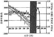
도 1은 평탄화 처리 동작과 같은 처리 동작 동안 모니터링되는 반도체 웨이퍼의 두께의 시간에 대한 그래프이다. 선 (100) 은 처리 동작 동안 종점/전이점을 검출하기 위한 적외선 (IR) 기초 센서와 관련된 값을 나타낸다. 선 (102) 은 처리 동안 시간에 따른 반도체 웨이퍼의 두께를 캡처하기 위한 복수의 와상 전류 센서 (ECS) 와 관련된 값을 나타낸다. 도시된 바와 같이, 영역 (104) 은 종점/전이점이 발생하는 곳의 시간을 나타낸다. 영역 (104) 에서, 일반적 기울기는 선 (102) 과 선 (100) 의 전이와 관련된다. 그러나, 적외선 모니터링 또는 와상 전류 모니터링 중 하나를 위해 모니터링되는 신호는 실행시마다 바뀌는 중대하고 변화가능한 배경 잡음이 부가된다. 따라서, 종점을 결정하기 위한 미분에 기초한 기울기를 측정할 때, 신호 대 잡음비 수준은 종점 결정의 안정성과 신뢰성에 영향을 미친다. 그러므로, 기울기에 기초한 분석에 입각한 전이점의 인-라인 (in-line) 결정은 반도체 동작을 위해 필수적인 확실한 데이터를 제공하지 않는다.1 is a graph of the time of the thickness of a semiconductor wafer monitored during a processing operation, such as a planarization processing operation.
따라서, 전이점이 모니터링된 처리 파라미터의 기울기에 기초한 전이를 통해 발생하는 처리를 위한 안정성 있고 신뢰성 있는 전이점 결정을 제공하기 위한 방법 및 장치를 제공하기 위해 선행 기술의 문제를 해결하기 위한 필요성이 있다.Accordingly, there is a need to address the problems of the prior art to provide a method and apparatus for providing stable and reliable transition point determination for processing that occurs through transitions based on the slope of the monitored process parameter.
발명의 요약Summary of the Invention
대체로 말하면, 본 발명은 전이점 결정의 신뢰성과 안정성을 개선시키기 위해서 미분에 기초한 데이터를 분석할 필요를 없애고 임계값 분석을 통한 전이점의 결정을 가능케 함으로써 상기 문제를 해결한다. 본 발명은 방법, 시스템, 컴퓨터 판독가능 매체 또는 장치를 포함한 다양한 방법으로 수행될 수 있다. 본 발명의 몇 개의 독창적인 실시형태가 아래에 설명된다.Generally speaking, the present invention solves this problem by eliminating the need to analyze data based on differentials to improve the reliability and stability of the transition point determination and enabling determination of the transition point through threshold analysis. The invention can be carried out in various ways, including as a method, a system, a computer readable medium or an apparatus. Several inventive embodiments of the present invention are described below.
일 실시형태에서, 기울기 기초 검출 태스크를 임계값 기초 검출 태스크로 변환하는 방법이 제공된다. 위의 방법은 모니터링되는 처리의 값에 대응하는 일 세트의 점들에 대한 근사 방정식을 정의함으로써 시작된다. 다음으로, 모니터링되는 처리의 현재점에서의 예상값이 예측된다. 다음으로, 모니터링되는 처리의 현재점에서의 측정값과 그에 대응하는 예상값 사이의 차이가 계산된다. 다음으로, 그 차이는 측정값과 예상값 사이의 편차값을 검출하기 위한 연속적인 점들을 위해 모니터링된다. 그 후, 모니터링되는 처리에 대한 전이점이 편차값의 검출에 기초하여 식별된다.In one embodiment, a method of converting a slope based detection task into a threshold based detection task is provided. The above method begins by defining an approximation equation for a set of points corresponding to the value of the monitored process. Next, an expected value at the present point of the monitored process is predicted. Next, the difference between the measured value at the present point of the monitored process and the corresponding expected value is calculated. Next, the difference is monitored for successive points for detecting a deviation between the measured value and the expected value. Then, the transition point for the monitored process is identified based on the detection of the deviation value.
다른 실시형태에서, 임계값 검출을 통한 기울기에 기초한 변화의 전이점을 검출하기 위한 방법이 제공된다. 그 방법은 전이점과 관련된 파라미터를 모니터링함과 함께 시작한다. 다음으로, 파라미터의 예상값은 모니터링된 처리 파라미터의 과거 값으로부터 계산된다. 예상값은 모니터링되는 처리 파라미터의 현재값에 대응한다. 다음으로, 임계값이 정의된다. 현재값과 예상값 사이의 차이가 탐지된다. 다음으로, 그 차이가 임계값을 초과할 때 전이점이 식별된다.In another embodiment, a method for detecting a transition point of change based on slope through threshold detection is provided. The method starts with monitoring the parameters associated with the transition point. Next, the expected value of the parameter is calculated from the past value of the monitored processing parameter. The expected value corresponds to the current value of the process parameter being monitored. Next, the threshold is defined. The difference between the present value and the expected value is detected. Next, the transition point is identified when the difference exceeds the threshold.
또 다른 실시형태에서, 실시간으로 임계값 결정을 통한 기울기 변화 전이를 위한 전이점이 검출가능한 반도체 처리 시스템이 제공된다. 시스템은 처리되는 반도체 웨이퍼와 관련된 정의된 파라미터가 얻어지도록 반도체 웨이퍼를 처리하도록 이루어진 처리 모듈을 포함한다. 처리 시스템은 처리 동작과 관련된 처리 파라미터를 모니터링하도록 이루어지는 센서를 포함한다. 그 시스템은 센서와 통신하는 검출기를 포함한다. 검출기는 측정값과 예상값을 비교하도록 이루어지고, 측정값은 기울기 변화를 통한 전이점을 나타낸다. 예상값은 미리 측정된 값으로부터 유도된다. 검출기는 임계값 편차값이 정의되도록 할 수 있기 위해 전이점에서의 변화를 강화하기 위한 측정값과 그에 대응하는 예상값 사이의 차이를 추적하도록 더 이루어진다. 임계값 편차값은 처리 동작과 관련된 전이점을 나타낸다.In yet another embodiment, a semiconductor processing system is provided that detects transition points for gradient change transitions in real time through threshold determination. The system includes a processing module configured to process the semiconductor wafer such that defined parameters associated with the semiconductor wafer being processed are obtained. The processing system includes a sensor configured to monitor the processing parameters associated with the processing operation. The system includes a detector in communication with the sensor. The detector is made to compare the measured value with the expected value, and the measured value represents the transition point through the change of the slope. The expected value is derived from the previously measured value. The detector is further configured to track the difference between the measured value and the corresponding expected value to enhance the change at the transition point so that the threshold deviation value can be defined. Threshold deviation values represent transition points associated with processing operations.
또 다른 실시형태에서, 기울기 기초 검출 태스크를 임계값 기초 검출 태스크로 변환하는 프로그램 명령을 갖는 컴퓨터 판독가능 매체가 제공된다. 컴퓨터 판독가능 매체는 모니터링되는 처리의 값에 대응하는 일 세트의 점들에 대한 근사 방정식을 정의하는 프로그램 명령과 모니터링되는 처리의 현재 점들에서 예상값을 예측하기 위한 프로그램 명령을 포함한다. 모니터링되는 처리의 현재점에서의 측정값과 그에 대응하는 예상값 사이의 차이를 계산하기 위한 프로그램 명령들이 제공된다. 측정값과 예상값 사이의 편차값을 검출하기 위한 차이를 모니터링하기 위한 프로그램 명령들과 편차값의 검출에 기초한 모니터링되는 처리에 대한 전이점을 식별하기 위한 프로그램 명령들이 포함된다.In yet another embodiment, a computer readable medium having program instructions for converting a slope based detection task into a threshold based detection task is provided. The computer readable medium includes program instructions for defining an approximation equation for a set of points corresponding to values of a monitored process and program instructions for predicting an expected value at current points of the monitored process. Program instructions are provided for calculating the difference between the measured value at the current point of the monitored process and the corresponding expected value. Program instructions for monitoring the difference for detecting the deviation value between the measured value and the expected value and program instructions for identifying the transition point for the monitored process based on the detection of the deviation value are included.
이하, 본 발명의 다른 양태와 이점을 본 발명의 원리를 예를 들어 설명한 첨부한 도면을 통하여 상세한 설명부에서 자세히 설명한다.Other aspects and advantages of the present invention will now be described more fully hereinafter with the accompanying drawings, which illustrate, by way of example, the principles of the invention.
도면의 간단한 설명Brief description of the drawings
본 발명은 첨부한 도면과 결합한 다음의 상세한 설명에 의해 쉽게 이해될 것이며, 동일한 도면부호는 동일한 구성요소를 나타낸다.BRIEF DESCRIPTION OF THE DRAWINGS The present invention will be readily understood by the following detailed description in conjunction with the accompanying drawings, wherein like reference numerals designate like elements.
도 1 은 평탄화 처리 동작과 같은 처리 동작 동안 모니터링되는 반도체 웨이퍼의 두께의 시간에 따른 그래프이다.1 is a graph over time of the thickness of a semiconductor wafer monitored during a processing operation, such as a planarization processing operation.
도 2 는 본 발명의 일 실시형태에 따라 전이점을 보여주기 위해 전이 영역에서의 잡음 수준이 평탄해지는 곳에서 적외선 기초 트레이스를 나타내는 그래프이다.FIG. 2 is a graph showing infrared based traces where noise levels in the transition region are flattened to show transition points in accordance with one embodiment of the present invention.
도 3 은 전이점을 포함하는 시간 동안 시간에 따른 신호 트레이스의 대표적인 그래프이다.3 is a representative graph of signal traces over time for a time period including transition points.
도 4 는 잡음을 제거하기 위해 평탄화된 도 3의 신호의 대표적인 그래프이다.4 is a representative graph of the signal of FIG. 3 flattened to remove noise.
도 5 는 본 발명의 일 실시형태에 따른 도 3의 실제 신호의 점들로부터 발생된 예측 신호의 대표적인 그래프이다.5 is a representative graph of a prediction signal generated from the points of the actual signal of FIG. 3 in accordance with an embodiment of the present invention.
도 6 은 본 발명의 일 실시형태에 따른 다양한 시점들에서의 실제 신호와 그에 대응하는 예측 신호 사이의 차이를 계산함으로써 발생되는 편차 신호의 대표적인 그래프이다.6 is a representative graph of a deviation signal generated by calculating a difference between a real signal at various time points and a corresponding prediction signal in accordance with one embodiment of the present invention.
도 7 은 본 발명의 일 실시형태에 따른 전이점에 대한 임계값 결정을 설명하기 위해 서로 겹쳐진 도 4, 도 5 및 도 6의 그래프를 포함하는 대표적인 그래프이다.7 is a representative graph including the graphs of FIGS. 4, 5 and 6 superimposed on one another to illustrate threshold determination for transition points in accordance with one embodiment of the present invention.
도 8a 는 본 발명의 일 실시예에 따른 실제 신호와 예측 신호의 트레이스를 설명하는 대표적인 그래프이다.8A is a representative graph illustrating a trace of an actual signal and a prediction signal according to an embodiment of the present invention.
도 8b 는 본래 신호값의 그래프와 그에 대응하는 본 발명의 일 실시형태에 따른 실제 신호와 예측 신호 사이의 편차의 그래프이다.8B is a graph of the original signal values and the corresponding deviations between the actual signal and the predicted signal according to one embodiment of the present invention.
도 8c 는 예상값 트레이스와 함께 겹쳐지는 도 8a와 도 8b의 실제 트레이스와 델타 트레이스의 그래프이며, 상기 그래프들은 본 발명의 일 실시형태에 따라 기울기 기초 태스크를 임계값 기초 태스크로 변환하기 위해 사용된다.8C is a graph of the actual and delta traces of FIGS. 8A and 8B superimposed with expected value traces, which are used to convert the slope based task into a threshold based task in accordance with one embodiment of the present invention. .
도 9 는 본 발명의 일 실시형태에 따라 기울기 기초 검출 태스크를 임계값 기초 검출 태스크로 변환하는 방법을 위한 방법 동작의 흐름도이다.9 is a flowchart of a method operation for a method for converting a slope based detection task into a threshold based detection task in accordance with an embodiment of the present invention.
도 10 은 본 발명의 일 실시형태에 따라 기울기 검출 전이점을 임계값 검출 전이점으로 변환하도록 이루어지는 검출기와 통신하는 처리 모듈의 고-수준 개략도이다.10 is a high-level schematic diagram of a processing module in communication with a detector configured to convert a slope detection transition point into a threshold detection transition point in accordance with an embodiment of the present invention.
도 11 은 본 발명의 일 실시형태에 따라 처리되는 반도체 기판의 전이점을 결정하기 위한 적외선 센서를 갖는 CMP 시스템의 간략화된 개략도이다.11 is a simplified schematic diagram of a CMP system having an infrared sensor for determining the transition point of a semiconductor substrate processed according to one embodiment of the present invention.
도 12 는 본 발명의 일 실시형태에 따라 처리되는 반도체 기판의 전이점을 결정하도록 이루어지는 와상 전류 센서를 갖는 처리 시스템의 간략화된 개략도이다.12 is a simplified schematic diagram of a processing system having an eddy current sensor configured to determine a transition point of a semiconductor substrate to be processed in accordance with an embodiment of the present invention.
바람직한 실시형태의 상세한 설명Detailed Description of the Preferred Embodiments
발명은 반도체 처리 동작 동안 전이점의 신뢰성있고 안정성있는 측정을 제공하는 시스템, 장치 및 방법에 대해 설명된다. 그러나, 당업자에게 본 발명이 이러한 특정한 상세한 설명의 일부 또는 전체 없이 수행될 수 있다는 것은 명백하다. 다른 예들에서, 잘 알려진 처리 동작들은 본 발명을 불필요하게 불명료하게 하지 않도록 하기 위해 상세하게 설명되지 않았다. 도 1은 발명의 배경 부분에 설명된다.The invention is described in systems, apparatus and methods that provide a reliable and stable measurement of transition points during semiconductor processing operations. However, it will be apparent to one skilled in the art that the present invention may be practiced without some or all of these specific details. In other instances, well known processing operations have not been described in detail in order not to unnecessarily obscure the present invention. 1 is described in the background section of the invention.
본 발명의 실시형태는 전이를 나타내는 전이 특징들을 증폭시킬 뿐만 아니라 기울기 검출 태스크를 임계값 검출 태스크로 변환시키는 시스템과 방법을 제공한다. 임계값 가동은 0 또는 일정 신호의 배경에서 계단 모양 특성을 생산하고 더 간단한 검출 알고리즘, 더 높은 신호-대-잡음비 및 더욱 강한 검출능력을 제공한다. 전이점/종점에 대한 임계값 기초 결정은 기울기 기초 결정에 비해 증가된 안정성 및 신뢰성을 제공한다. 차례로, 더욱 안정성있고 신뢰성있는 트리거(trigger) 조건이 반도체 처리에 대해 제공된다. 즉, 전이점/종점이 높은 정도의 확실성과 함께 결정되기 때문에, 실질적으로 정밀한 측정을 요구하는 하류부분의 동작은 인-라인 계측을 통해 시작될 수 있다. 따라서, 관련된 동작에 대한 반도체 처리량 (throughput) 은 부수적으로 증가할 수 있다. 미분 분석에 대한 신호를 추적하는 처리의 기울기의 작은 변화로부터 발생하는 복잡성은 신호 추적의 임계값 형태로의 변환에 의해 제거된다. 여기서 사용된 용어인 종점과 전이점은 번갈아 사용할 수 있다. 종점 및 전이점이라는 용어은 표적 변화가 발생하고, 표적 상태가 달성되거나, 또는 모니터링되는 파라미터와 관련된 특정 값의 달성이 다른 처리 동작의 종점이나 시작과 같은 일을 트리거하는데 사용되는 반도체 처리 또는 다른 어떤 처리에서 어떤점이든 가리킬 수 있다는 것은 당업자에게 명백할 것이다.Embodiments of the present invention provide a system and method for amplifying transition features indicative of transitions as well as converting a slope detection task into a threshold detection task. Threshold operation produces stepped characteristics in the background of zero or constant signals and provides simpler detection algorithms, higher signal-to-noise ratios and stronger detection capabilities. Threshold based determinations for transition points / endpoints provide increased stability and reliability compared to slope based determinations. In turn, more stable and reliable trigger conditions are provided for semiconductor processing. In other words, since the transition point / end point is determined with a high degree of certainty, the operation of the downstream part requiring substantially precise measurements can be initiated through in-line metrology. Thus, semiconductor throughput for related operations may increase incidentally. The complexity arising from small changes in the slope of the process tracking the signal for differential analysis is eliminated by the conversion of the signal tracking to the threshold form. The term end point and transition point used herein may be used interchangeably. The term end point and transition point refer to a semiconductor process or any other process in which a target change occurs, the target state is achieved, or the achievement of a particular value related to the parameter being monitored is used to trigger a task such as the end or the beginning of another processing operation. It will be apparent to those skilled in the art that any point in the FIG.
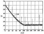
도 2는 본 발명의 일 실시형태에 따라 전이점을 보여주기 위해 전이 영역에서의 잡음 수준이 평탄화되는 적외선 (IR) 기초 트레이스의 그래프이다. 여기서, 영역 (106) 에서는 잡음 수준이 실질적으로 제거되어, 트레이스 (108) 가 평탄화된 라인으로 나타난다. 도시된 바와 같이, 평탄화된 트레이스 (108) 와 관련된 기울기는 영역 (106) 에서 전이한다. 그러나, 모니터링되는 동작, 예컨대, 화학적 기계적 평탄화 (CMP) 동작 또는 식각 동작과 관련된 잡음은, 종점 또는 다른 동작의 시작과 같은 일을 트리거하기 위한 실시간의 안정적이고 재생가능한 기록을 방해한다. 도 2 에서는 온도와 관련된 적외선 신호를 도시하고 있지만, 다른 신호들, 예컨대, 와상 전류 센서, 진동, 광학 굴절 등은 유사한 특성을 보일 것이다. 즉, 평탄화된 기울기는 전이점을 나타낼 것이다. 그러나, 상술한 바와 같이, 배경 잡음 때문에 기울기 판독으로부터 안정성있고 정확한 실시간 판독을 할 수 없다. 이하에서 더욱 상세하게 설명되겠지만, 기울기 측정에서 임계값 측정으로의 변환은 기울기 측정과 관련된 미분 측정에 대해 분석되는 작은 차이에 영향을 미치는 잡음 수준과 관련된 불확실성을 제거한다. 따라서, 실시간으로, 더욱 정확한 전이점의 검출이 가능해진다. 전이점을 나타내는 기울기의 작은 변화는 기울기 측정의 잡음에 의해 가려지지만, 여기에 설명된 실시형태는 실질적으로 잡음이 전이점의 결정에 영향을 주는 것을 방지한다.2 is a graph of infrared (IR) based traces where the noise level in the transition region is flattened to show the transition point in accordance with one embodiment of the present invention. Here, in the
도 3은 시간에 따른 신호 트레이스의 대표적인 그래프이며, 시간의 주기는 전이점을 포함한다. 여기서, 신호 (110) 는 시간 경과에 따라 작성된다. 일 실시형태에서, 신호 (110) 는 반도체 동작 동안의 전이점을 나타내는 처리 파라미터를 검출하도록 이루어지는 와상 전류 센서로부터 시작된다. 반도체 동작 동안의 전이점을 검출하기 위한 다른 신호들은 적외선, 진동, 광학-기초 신호, 등과 같은 것에 포함될 수 있다. 도시된 바와 같이, 신호 (110) 는 신호와 관련된 상당한 양의 잡음을 갖지만, 시간에 따른 추세는 시간 (100) 에서의 전이점을 나타낸다. 여기서 당업자는 배경 잡음으로 인하여, 기울기 기초 결정에 있어 불안정한 결과를 산출할 것이다.3 is a representative graph of signal traces over time, wherein the period of time includes a transition point. Here, signal 110 is created over time. In one embodiment, signal 110 begins with an eddy current sensor configured to detect processing parameters indicative of transition points during semiconductor operation. Other signals for detecting transition points during semiconductor operation may be included, such as infrared, vibration, optical-based signals, and the like. As shown, signal 110 has a significant amount of noise associated with the signal, but the trend over time represents a transition point in
도 4는 잡음을 제거하기 위해 평탄화된 도 3의 신호의 대표적인 그래프이다. 여기서, 선 (110a) 은 신호를 평탄화시기키 위해 적용된 정규 사인곡선 잡음 필터를 가졌다. 신호 (110a) 는 시간에 따른 와상 전류 센서의 값을 나타내며, 전이점은 대략 시간 (100) 에서의 기울기의 변화에 의해 나타난다. 상술한 바와 같이, 평탄화된 기울기는 실시간으로 안정성있고 정확한 방법으로 만들어질 수 없다. 그러므로, 기울기 기초 결정은 여기서 확실한 대안이 될 수 없다.4 is a representative graph of the signal of FIG. 3 flattened to remove noise. Here, line 110a has a regular sinusoidal noise filter applied to smooth the signal. Signal 110a represents the value of the eddy current sensor over time, and the transition point is represented by a change in slope at approximately
도 5는 본 발명의 일 실시형태에 따른 도 3의 실제 신호의 점들로부터 발생된 예측 신호의 대표적인 그래프이다. 여기서, 데이터 흐름 점들의 선택된 구간에 대한 근사 방정식은 본 발명의 일 실시형태에서 가장 최근의 데이터 기록을 예측하는데 사용된다. 도 8a와 도 8b를 참조하여 더욱 상세하게 설명되겠지만, 예측 신호는 본 발명의 일 실시형태에 따른 예측된 실시간 데이터 점을 생성하기 위해 근사 방정식을 실제 신호의 역사적 데이터 점들에 적용함으로써 생성된다. 도 5에 도시된 바와 같이, 선 (110b) 에 의해 나타낸 예측된 신호는 시간 (100) 에서 도 3과 도 4의 실제 신호로부터 벗어나기 시작하며, 그것이 전이점을 나타낸다. 근사 방정식은 어떤 다항식일 수도 있다. 예를 들어, 근사 방정식은 선형 방정식, 포물선 방정식 또는 어떤 다른 고차 방정식일 수도 있다.5 is a representative graph of a prediction signal generated from the points of the actual signal of FIG. 3 in accordance with an embodiment of the present invention. Here, an approximation equation for the selected interval of data flow points is used to predict the most recent data record in one embodiment of the present invention. As will be described in more detail with reference to FIGS. 8A and 8B, the prediction signal is generated by applying an approximation equation to the historical data points of the actual signal to generate the predicted real-time data point according to one embodiment of the invention. As shown in FIG. 5, the predicted signal represented by
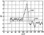
도 6은 본 발명의 일 실시형태에 따른 다양한 시점들에서의 실제 신호와 그에 대응하는 예측 신호 사이의 차이를 계산함으로써 생성되는 편차 신호의 대표적인 그래프이다. 여기서, 선 (112) 은 시간에 따른 예측 신호와 실제 신호 사이의 차이를 나타낸다. 영역 (114) 은 잡음 통로를 나타낸다. 즉, 오프셋이 잡음 통로를 정의하기 위해 실제 신호와 예측 신호 사이의 차이에 적용될 수 있으며, 잡음 통로 외측의 점들이 전이점에 대한 유효점으로 고려될 수 있다. 본질적으로, 잡음 통로는 실제 값과 예측 값 사이의 차이에 관한 경계 (boundary) 를 정의한다. 일 실시형태에서, 오프셋은 표준편차 값의 3배, 즉 3σ로 선택된다. 그러므로, 잡음 분포가 가우시안 분포로 구성된다면 3σ는 분포의 모든 점들의 99.7 %를 커버할 수 있다. 그러므로, 1000개의 점중, 실제로 잡음 통로 외측 에 존재하고 전이점의 시작이 되지 않을 3 × 10⁻³ 의 확률이 한 점에 존재한다. 모니터링되는 처리의 성질에 따라, 이 확률은 정확도의 수용가능한 수준을 제공하기 위해 감소되거나 증가될 수 있다.6 is a representative graph of a deviation signal generated by calculating a difference between a real signal at various time points and a corresponding prediction signal in accordance with one embodiment of the present invention. Here,
도 7은 본 발명의 일 실시형태에 따른 전이점에 대한 임계값 결정을 설명하기 위해 서로 겹쳐진 도 4, 도 5 및 도 6의 그래프를 포함하는 대표적인 그래프이다. 여기서, 도 4로부터의 선 (110a), 도 5로부터의 선 (110b) 및 선 (112) 은 서로 겹쳐진다. 또한, 잡음 (114) 의 통로도 설명된다. 편차 신호, 즉 실제 신호와 예측 신호 사이의 차이를 나타내는 선 (112) 은 시간 (100) 의 전이점에서 잡음 통로를 초과하기 시작한다. 아래에서 더욱 상세하게 설명되겠지만, (잡음의) 3σ 통로는 전이점이 검출되기 시작하는 더 높은 또는 더 낮은 신뢰 수준을 제공하기 위해 조정된다. 예컨대, 높은 정도의 정확도와 정밀도를 요구하는 처리는 더 낮은 정도의 정확도와 정밀도를 요구하는 처리보다 더 넓은 잡음 통로를 사용할 수 있다. 다른 실시형태에서, 잡음 통로의 경계 외측의 2개 이상의 연속점은 전이점 알림을 트리거하기 위해 요구될 수 있다.7 is a representative graph including the graphs of FIGS. 4, 5, and 6 superimposed on one another to illustrate threshold determination for transition points in accordance with one embodiment of the present invention. Here, the line 110a from FIG. 4, the
도 8a는 본 발명의 일 실시형태에 따른 실제 신호와 예측 신호의 트레이스를 설명한 대표적인 그래프이다. 선 (120) 은 시간에 따른 처리 파라미터 기록의 점들을 나타낸다. 일 실시형태에서 처리 파라미터는 막의 두께와 관련이 있다. 그래프의 영역 (121) 은 전이전 (pre-transition) 영역을 나타내며, 반면 그래프의 영역 (123) 은 전이후 (post transition) 영역을 나타낸다. 따라서, 선 (120) 은 2개의 연속처리, 예컨대, 전이전 영역 처리와 전이후 영역 처리를 나타내며, 두 처리 사이에 전이점의 형태에서의 단절이 있다. 여기서 전이점은 한 상태에서 다른 상태로의 변화를 나타낸다. 여기서 설명된 실시 형태는 반도체 처리를 언급하지만, 방법론은 전이가 발생하는 어떤 시스템에도 적용될 수 있으며, 기울기 검출 처리는 한 상태로부터 다른 상태로 전이를 포착할 수도 있다.8A is a representative graph illustrating traces of an actual signal and a prediction signal in accordance with an embodiment of the present invention.
도 8a를 참조하면, 이전의 부분 또는 데이터의 구간, 예컨대 영역 (121) 의 n 부분은 나중 시점에서의 값을 예측하기 위해 사용된다. 일 실시형태에서, 포물선 방정식과 같은 다항식이 가장 최근의 데이터 기록에 대응하는 예상값을 유도하기 위해 사용된다. 여기서, 데이터 구간이라고도 언급되는 데이터의 부분이 선택되고 거리 m 이 계산됨으로써 데이터 값이 산출된다. 당업자는 일 실시형태에서 포물선 (또는 고차 급수) 근사식이Referring to FIG. 8A, the previous portion or interval of data, such as the n portion of
Y=a1tn+a2tn-1+...+anY = a1 tn + a2 tn-1 + ... + an
의 형태로 데이터 값을 산출하기 위해 사용되며, 여기서 Y는 예상값 (y 좌표값) 을 나타내고, t는 시간 (x 좌표값) 을 나타낸다. 물론, 이전의 데이터는 데이터와 관련된 각각의 영역의 다이나믹스를 나타낸다.Is used to calculate the data value in the form of, where Y represents the expected value (y coordinate value) and t represents time (x coordinate value). Of course, the previous data represents the dynamics of each area associated with the data.
따라서, 검출 장치, 즉, 센서에 의해 측정된 실제 신호는 근사 방정식으로부터 계산된 예측 신호와 비교될 수 있다. 실제 신호와 예측 신호는 전이가 발생하지 않고 예상 (외삽법: extrapolation) 거리가 너무 크지 않는한 실질적으로 같다. 즉, 실제 신호값과 예측 신호값 사이의 차이 (Si-Y로 나타낸 Si는 실제 신호이고 Y는 예측 신호인) 는 잡음 수준 내에서 0에 가깝다. 그러나, 일단 전이가 발생하면 실제 신호와 예측 신호 사이의 차이는 도 8a의 Δ 122로 나타낸 바와 같이, 점점 0보다 커지기 시작한다, Si-Y〉0. 따라서, 임계값은 어디에서 실제 신호와 예상값이 빗나가는지 검출하기 위해 사용될 수도 있다. 더 설명되겠지만, 기울기 검출 처리에서 임계값 검출 처리로의 변환은 변화와 관련된 전이를 강화 (증폭) 시켜서 전이가 더욱 정확하고 정밀하게 식별될 수 있게 한다.Thus, the actual signal measured by the detection device, ie the sensor, can be compared with the predictive signal calculated from the approximation equation. The actual and predicted signals are substantially the same as long as no transition occurs and the expected (extrapolation) distance is not too large. That is, the difference between the actual signal value and the predicted signal value (Si denoted by Si-Y is the real signal and Y is the predicted signal) is close to zero within the noise level. However, once a transition occurs, the difference between the actual signal and the predicted signal begins to grow larger than zero, as indicated by
도 8b는 본 발명의 실시형태에 따른 원래 신호값의 그래프와 그에 대응하는 실제 신호와 예측 신호 사이의 편차의 그래프이다. 도 8b의 상측 그래프는 도 8a의 실제 신호를 나타낸다. 예컨대, 반도체 처리 모니터링에 관하여, 선 (120) 은 적외선 센서, 와상 전류 센서, 진동 센서, 온도 센서, 반사 스펙트럼을 검출하도록 이루어지는 센서 등으로부터의 신호와 관련된 트레이스를 나타낸다. 시간 tt에서 발생하는 전이는 델타 트레이스라고도 언급되는 편차 트레이스 128을 통해서 검출된다. 영역 (124,126) 은 예상값이 실제 신호로부터 각각 포지티브 및 네거티브 차이들로서 실제 신호로부터 빗나가는 영역을 나타낸다.8B is a graph of the original signal value and the deviation between the corresponding real signal and the predicted signal according to an embodiment of the present invention. The upper graph of FIG. 8B shows the actual signal of FIG. 8A. For example, with respect to semiconductor process monitoring,
도 8b의 델타 트레이스 (128) 는 시간에 따른 실제 신호와 예측신호 사이의 차이를 나타낸다. 영역 (114) 은 잡음 통로를 나타낸다. 델타 트레이스 (128) 와 실제 신호의 트레이스 (120) 는 각각의 트레이스와 관련된 배경 잡음을 가지기 쉽다. 따라서, 트레이스 (120) 는 도 3의 트레이스와 유사하기 쉽고, 델타 트레이스 (128) 는 도 6의 트레이스와 유사하기 쉽다. 즉, 트레이스들은 평탄한 선보다는 각각의 트레이스와 관련된 잡음을 가지기 쉽다. 따라서, 잡음 통로는 잡음 수준이 전이점의 결정에 영향을 주지 않도록 잡음 수준을 고려하도록 이루어진다. 동시에, 잡음 통로의 오프셋이라고도 언급되는, 크기가 전이가 잡음 수준 위에서 발생하도록, 즉, 잡음 통로가 전이점을 가릴만큼 크지 않도록 선택된다.
일 실시형태에서, 잡음 통로의 오프셋은 델타 트레이스 (128) 의 3 표준편차 (3σ) 에서 설정된다. 따라서, 잡음이 가우시안 분포인 곳에서, 3σ는 분포의 모든 점들의 99.7 %를 커버할 수 있다. 상술한 바와 같이, 잡음 통로 밖으로 떨어지고 전이점의 시작이 되지 않을 3 × 10⁻³ 의 확률이 한 점에 존재하는데, 각 1000개의 점중 3개가 실제로 정의된 3σ 구간의 외측에 존재할 수 있다는 의미이다. 더 설명되겠지만, 도 9를 참조하면, 거짓 포지티브 (false positive) 의 확률을 더욱 감소시키기 위해 잡음 통로의 외측의 많은 연속점들이 전이점의 시작을 나타내기 위해 필요할 수 있다. 일 실시형태에서, 만약 상당히 많은 수의 잡음의 통로 외측의 연속점들이 사용되거나 3σ 보다 큰 잡음 통로가 사용된다면, 오프셋은 필요하지 않을 수도 있다. 어떤 수의 잡음 통로 외측의 연속점도 전이점을 위한 트리거로서 정의될 수 있다. 전이점에 도달되는 것을 나타내기 위해 요구되는 연속점들의 숫자가 많아질수록, 실제 전이점이 얻어지는 확실성도 커진다. 따라서, 거짓 포지티브인 정확한 동작이 비용이 많이 들고 회복 불가능한 손상을 트리거하기 때문에, 잡음 통로 밖의 3 개 이상의 점들이 높은 정도의 신뢰를 제공하기 위해 선택될 수도 있다. 처리가 그리 까다롭지 않다면 2개 이하의 점을 선택하는 것이 바람직할 수도 있다.In one embodiment, the offset of the noise path is set at three standard deviations (3σ) of the
도 8c는 예측된 값의 트레이스가 첨가된 도 8a와 도 8b의 실제 트레이스와 델타 트레이스를 설명한 그래프이며, 세 그래프는 모두 본 발명의 일 실시형태에 따라 기울기 기초 태스크를 임계값 기초 태스크로 변환하는데 사용된다. 트레이스 (120) 는 실제 센서 기록을 나타낸다. 트레이스 (136) 는 포물선으로 외삽된 예상값을 나타낸다. 트레이스 (128) 는 실제 센서 기록과 그에 대응하는 예상값 사이의 차이인 델타 트레이스를 나타낸다. 포물선으로 외삽된 예상값은 데이터 점들의 선택된 구간과 관련된 포물선 근사법과 가장 최근의 데이터 기록에 대한 포물선 예측을 포함한다. 델타 트레이스 (128) 는 현재점에 대해 포물선으로 외삽된 예상값과 많은 앞의 연속점들을 감산하여 계산된다. 따라서, 임계값은 델타 트레이스가 안정적으로 잡음 수준 위에 있을때 정의될 수 있다. 예컨대, 전이점이 발생하는 것을 알기 전에 잡음 수준 외측의 많은 연속점을 정의하는 것은 전이점 결정이 정확한 높은 신뢰도의 수준을 제공할 것이다. 당업자는 전이점이 여기서 사용된 종점을 포함한다는 것을 이해할 수 있을 것이다. 이 실시형태에서 포물선 방정식은 근사 방정식으로 사용되는 반면, 실제 센서 기록에 의해 정의된 곡선의 모양이 근사 방정식의 형태에 영향을 주기 때문에 어떤 다항식도 근사방정식으로 사용될 수 있다.FIG. 8C is a graph illustrating the actual and delta traces of FIGS. 8A and 8B with the traces of the predicted values added, all three graphs for converting the slope based task into a threshold based task in accordance with one embodiment of the present invention. Used.
도 3과 도 6을 참조하면, 도 6의 델타 트레이스 근사법의 임계값 결정은 도 3의 기울기 기초 근사법보다 뛰어나다. 즉, 기울기 기초 결정에서의 잡음은 기울기에서의 작은 변화를 가리며 (hide) 반면 임계값 기초 결정에서의 잡음은 전이점의 인식을 시작하기 전에 오프셋을 정의하거나 잡음 통로의 외측의 많은 연속점들을 필요로 함으로써 제거된다. 일단 전이점이 달성되면 다른 정의된 동작이 시작될 수도 있고 또는 현재 처리에 대한 종점이 발생할 수도 있다. 반도체 제조, 예컨대, 식각, 증착, CMP 동작 또는 다른 어떤 표면 변형 처리에 관련하여, 첫번째 층이 추가, 제거, 평탄화 또는 변형될 수도 있으며, 그 후 반도체 웨이퍼는 처리 도구 또는 다른 처리 도구에서의 또 다른 모듈로 전이될 수도 있다.3 and 6, the threshold determination of the delta trace approximation of FIG. 6 is superior to the slope based approximation of FIG. 3. In other words, the noise in the slope-based determination hides a small change in the slope, while the noise in the threshold-based determination defines the offset before starting to recognize the transition point, or the many continuous points outside the noise path. It is removed as needed. Once the transition point is achieved, another defined action may begin or an endpoint for the current process may occur. In connection with semiconductor fabrication, such as etching, deposition, CMP operation, or any other surface modification treatment, the first layer may be added, removed, planarized, or otherwise deformed, and the semiconductor wafer may then be further processed in a processing tool or other processing tool. It may be transitioned to a module.
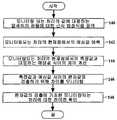
도 9는 본 발명의 일 실시형태에 따른 기울기 기초 검출 태스크를 임계값 기초 검출 태스크로 변환시키는 방법에 대한 방법 동작의 흐름도이다. 그 방법은 근사 방정식이 일 세트의 점들에 대해 정의되는 동작 (140) 과 함께 시작한다. 일 세트의 점들에 대한 근사 방정식은 모니터링되는 처리의 값에 대응한다. 예컨대, 위에서 논의된 바와 같이 포물선 방정식과 같은 다항식은 근사 방정식이 될 수 있다. 모니터링되는 처리는 와상 전류 센서, 적외선 센서, 온도 센서, 진동 센서 등을 통해서 모니터링될 수 있다. 그 방법은 그후 모니터링되는 처리의 현재점에서의 예상값이 예측되는 동작 (142) 을 진척시킨다. 여기서, 다항식은 많은 연속점들의 데이터 구간을 필요로 하며 현재점에 대한 예상값을 예측한다. 본질적으로, 다항식은 도 8a를 참고하여 설명된 바와 같이 과거의 데이터 점들로부터 현재점을 예상하는 것을 고려한다.9 is a flowchart of a method operation for a method of converting a slope based detection task into a threshold based detection task in accordance with an embodiment of the present invention. The method begins with
도 9의 방법은, 그후 처리의 현재점에서의 측정된 (실제) 값과 그에 대응하는 예상값의 차이가 계산되는 동작 (144) 으로 진행한다. 여기서, 측정값과 예상 (예측) 값 사이의 차이는 전이점까지 거의 0일 것이다. 그 차이는 두 값 사이의 감산에 의하여 측정될 수 있으나 이 차이의 해석으로 정의되지 않는다. 도 8a 내지 도 8c를 참조하면 전술한 바와 같이 차이는 델타 트레이스로 포착될 수도 있다. 따라서, 처리의 현재점에서의 측정값과 그에 대응하는 예상값 사이의 차이는 동작 (146) 에서의 편차값을 검출하기 위해 모니터링된다. 편차값은 잡음 통로 외측의 많은 연속점으로 정의될 수 있으며, 연속점의 갯수는 하나 이상일 수 있다. 다른 실시형태에서, 차이는 또한 비율, 차이의 제곱 등으로 계산될 수 있다. 즉, 여기서 사용된 용어인 차이는 두 값들 사이의 일반화된 차이를 나타내는 넓은 범위의 측정을 언급한다. 선택적으로, 오프셋이 사용될 수 있는데, 오프셋은 배경 잡음이 전이점을 나타내는 것을 피할 수 있을만큼 충분히 높고 전이점을 나타내는 편차값이 식별될 수 있도록, 즉, 오프셋에 의해 가려지지 않도록 충분히 낮다. 그 방법은 그 후 모니터링되는 처리에 대한 전이점이 편차값의 검출에 기초하여 식별되는 동작 (148) 으로 진행한다. 물론, 전이점은 현재 처리 동작을 종료시키고 다른 처리 동작을 트리거하거나 단순히 현재 처리를 종료시킬 수 있다.The method of FIG. 9 then proceeds to
도 10은 본 발명의 일 실시형태에 따라 기울기 검출 전이점을 임계값 검출 전이점으로 변환시키도록 이루어지는 검출기와 통신하는 처리 모듈의 고-수준 개략도이다. 처리 모듈 (160) 은 어떤 처리 모듈, 예컨대, CMP 모듈, 식각 모듈 등과 같은 어떤 관련된 반도체 처리 모듈도 될 수 있다. 검출기 (162) 는 처리 모듈 (160) 과 통신한다. 예컨대, 처리 모듈 (160) 의 내부에 위치한 센서들은 신호를 검출기 (162) 로 전달하기 위해 사용될 수 있다. 검출기 (162) 는 기울기가 전이점을 결정하는 처리를 임계값이 전이점을 검출하기 위해 사용되는 임계값 검출 처리로 변환시키도록 이루어진다. 즉, 도 8a, 8b, 8c 및 9를 참조하여 설명된 기울기 검출 처리를 임계값 검출 처리로 변환하는 실시예들은 검출기 (162) 에 의해 수행된다. 또한, 전이점에서 발생하는 변화들은 임계값이 쉽게 검출될 수 있도록 강화된다. 일 실시형태에서, 임계값이 여기에 설명된 바와 같이 실제 신호와 예측된 신호 사이의 차이로서 정의된다. 검출기 (162) 가 처리 모듈 (160) 에서 수행되는 처리 동작을 제어하는 일반적인 목적의 컴퓨터일 수도 있다. 검출기 (162) 는 아래에 설명된 바와 같이 조성 변화나 상태 변화를 모니터링하도록 이루어지는 센서로부터 신호들을 받을 수 있다. 물론, 처리 모듈 (160) 과 검출기 (162) 사이의 통신은 폐루프 (closed loop) 를 관통할 수도 있다.10 is a high-level schematic diagram of a processing module in communication with a detector configured to convert a slope detection transition point into a threshold detection transition point in accordance with an embodiment of the present invention.
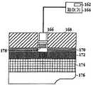
도 11은 본 발명의 일 실시형태에 따라 처리되는 반도체 기판의 전이점을 결정하기 위한 적외선 센서를 갖는 CMP 시스템의 간략화된 개략도이다. 제어기 (164) 는 검출기 (162) 를 포함한다. 제어기 (164) 는 적외선 센서 (166) 와 통신한다. 적외선 센서는 캐리어판 (168) 내에 포함된다. 반도체 기판 (172) 은 캐리어판 (168) 내의 캐리어막 (170) 에 기대어 지지된다. 적외선 센서 (166) 는 윈도우 (178) 를 통해서 반도체 기판 (172) 까지의 일렬의 시야를 갖는다. 연마 패드 (174) 는 반도체 기판 (172) 의 표면을 평탄화한다. 연마 패드 (174) 는 스테인레스 스틸 벨트 (176) 상부에 위치된다. 검출기 (162) 는 적외선 센서와 관련된 기울기 기초 신호 처리를 임계값 기초 신호로 변환시킨다. 일 실시형태에서, 도 8a, 도 8b, 도 8c 및 9를 참고하여 설명된 바와 같이 기울기 기초 신호는 실제 신호와 예측 신호 사이의 델타 트레이스를 정의함으로써 임계값 기초 동작으로 변환된다.11 is a simplified schematic diagram of a CMP system having an infrared sensor for determining the transition point of a semiconductor substrate processed in accordance with one embodiment of the present invention. Controller 164 includes a
도 12는 본 발명의 일 실시형태에 따라 처리되는 반도체 기판의 전이점을 결정하도록 이루어지는 와상 전류 센서를 갖는 처리 시스템의 간략화된 개략도이다. 제어기 (164) 는 검출기 (162) 를 포함한다. 제어기 (164) 는 와상 전류 센서 (180a,180b) 와 통신한다. 와상 전류 센서 (180a,180b) 는 반도체 기판 (162) 상부에 위치된 막의 두께와 같은 처리 파라미터를 모니터링하도록 이루어질 수도 있다. 처리 시스템이 CMP 처리 시스템인 경우, 연마 패드 (174) 는 반도체 기판 (172) 의 표면을 평탄화시킨다. 연마 패드 (174) 는 받침 (backing; 176) 의 상부에 위치된다. 검출기 (162) 는 와상 전류 센서 (180a,180b) 의 기울기 기초 검출 출력을 임계값 검출 처리로 변환시킨다. 여기서 다시, 검출기 (162) 는 전이점을 나타내는 임계값 편차값을 검출하기 위해서 측정값과 예측값 사이의 차이를 추적한다.12 is a simplified schematic diagram of a processing system having an eddy current sensor configured to determine a transition point of a semiconductor substrate to be processed in accordance with one embodiment of the present invention. Controller 164 includes a
도 11 및 도 12는 반도체 제조를 위해 사용되는 센서들의 특정한 실시형태를 그리고 있다. 여기서 설명된 실시형태는 조성 변화 또는 상태변화를 모니터링할 수 있는 어떤 형태의 센서와도 관련될 수 있다. 대표적인 조성 변화는 첫번째 층이 제거되고 두번째 층이 노출되거나 반도체 웨이퍼 같은 오브젝트의 표면이 변형되는 표면 조성 변화를 포함한다. 대표적인 상태 변화는 액체에서 기체로, 액체에서 고체로 등의 변화를 포함한다. 사실, 전이점은 조성 또는 상태 변화 가 발생하는 곳에서의 점으로 정의될 수 있다. 전이점에서, 여기서 설명된 센서를 통해 모니터링되는 특성은 처리 조건에 기인하여 변한다. 표적 특성은 두께, 저항, 평탄도, 투명도, 진동, 화학적 조성 등과 같은 특성을 포함한다. 여기 설명된 바와 같이 임계값 검출 계획에 의해 이 변화가 모니터링되고 전이점이 결정된다. 당업자는 여기에 설명된 실시형태가 상술한 특정한 형태의 센서에 정의되지 않는다는 것을 이해할 수 있을 것이다. 더욱 상세하게는, 센서들이 반도체 제조 처리와 관련이 있건 없건 간에 조성 또는 상태 변화를 나타내는 신호를 검출하도록 이루어진 어떤 센서도 상술한 실시형태들과 함께 사용될 수 있다. 또한, 센서들은 처리되는 오브젝트, 예컨대, 반도체 웨이퍼, 또는 처리 모듈의 성분, 예컨대, 연마 패드를 통한 변화를 검출할 수 있다. 따라서, 전이점은 직접적 또는 간접적으로 검출될 수 있다. 몇몇의 대표적인 센서들은 저항, 저장용량, 반사광, 진동 등을 검출하도록 이루어진 센서들을 포함한다.11 and 12 illustrate specific embodiments of sensors used for semiconductor fabrication. Embodiments described herein may relate to any type of sensor capable of monitoring compositional changes or state changes. Representative composition changes include surface composition changes in which the first layer is removed and the second layer is exposed or the surface of the object, such as a semiconductor wafer, is deformed. Representative state changes include changes from liquid to gas, from liquid to solid, and the like. In fact, a transition point can be defined as the point where a composition or state change occurs. At the transition point, the properties monitored through the sensors described herein change due to processing conditions. Target properties include properties such as thickness, resistance, flatness, transparency, vibration, chemical composition, and the like. This change is monitored and the transition point is determined by the threshold detection scheme as described herein. Those skilled in the art will appreciate that the embodiments described herein are not defined in the specific types of sensors described above. More specifically, any sensor configured to detect a signal indicative of a composition or state change, whether or not the sensors are associated with a semiconductor fabrication process, can be used with the embodiments described above. In addition, sensors can detect changes through the object being processed, such as a semiconductor wafer, or a component of the processing module, such as a polishing pad. Thus, the transition point can be detected directly or indirectly. Some representative sensors include sensors configured to detect resistance, storage capacity, reflected light, vibration, and the like.
요약에서, 상술한 발명은 기울기 기초 검출 태스크를 임계값 기초 검출 태스크로 변환하기 위한 방법 및 시스템을 설명한다. 다항식과 같은 근사 방정식은 현재 데이터 점에서 예상값을 예측하기 위해 사용된다. 예상값과 센서로 부터 제공된 실제 값 사이의 차이는 전이점을 검출하기 위해 모니터링된다. 모니터링된 차이는 여기에 설명된 바와 같이 델타 트레이스로 포착된다. 차이의 추적으로 임계값이 정의된다. 일 실시형태에서, 전이점은 모니터링된 차이의 미리 정의된 갯수의 연속 점들이 잡음 통로 외측에서 검출될 때 발생한다. 오프셋 경계 외측의 검출된 점, 즉, 실제값과 예상값 사이의 차이값이 전이점을 나타내는 수준을 정의하기 위해서 오프셋이 또한 제공될 수도 있다. 기울기 검출 태스크를 임계값 검출 태스크로 변환시킴으로써, 기울기 검출 태스크에 의해 요구되는 도함수 분석의 필요성을 없애는 안정성있고 신뢰성있는 전이 검출 시스템이 제공된다. 또한, 상술한 델타 트레이스는 더욱 쉽게 전이점을 식별하기 위해서 전이점에서 발생하는 변화를 강화시킨다.In summary, the above-described invention describes a method and system for converting a slope based detection task into a threshold based detection task. Approximate equations, such as polynomials, are used to predict the expected value at the current data point. The difference between the expected value and the actual value provided by the sensor is monitored to detect the transition point. The monitored difference is captured with a delta trace as described herein. The threshold is defined by tracking the difference. In one embodiment, the transition point occurs when a predefined number of consecutive points of the monitored difference are detected outside the noise path. An offset may also be provided to define the level at which a detected point outside the offset boundary, that is, the difference between the actual value and the expected value, represents the transition point. By converting the slope detection task into a threshold detection task, a stable and reliable transition detection system is provided that obviates the need for derivative analysis required by the slope detection task. In addition, the delta trace described above enhances the changes that occur at the transition point to more easily identify the transition point.
위의 실시형태를 염두에 두면, 본 발명은 컴퓨터 시스템에 저장된 데이터와 관련된 컴퓨터로 수행되는 다양한 동작을 사용할 수도 있다는 것이 이해될 것이다. 이러한 동작들은 물리적인 양의 물리적인 처리를 요구하는 동작을 포함한다. 통상적으로, 꼭 그렇지는 않지만, 이런 양은 저장되고, 이동되고, 결합되고, 비교되고, 그렇지 않으면 처리될 수 있는 전기적 또는 자기적 신호의 형태를 취한다. 또한, 수행되는 처리들은 종종 생산, 식별, 결정 또는 비교와 같은 용어로 언급된다.With the above embodiments in mind, it will be appreciated that the present invention may employ various operations performed by a computer related to data stored in a computer system. Such operations include operations requiring a physical amount of physical processing. Typically, but not necessarily, these quantities take the form of electrical or magnetic signals that can be stored, moved, combined, compared, or otherwise processed. In addition, the processes performed are often referred to in terms, such as production, identification, determination, or comparison.
상술한 발명은 소형 장치, 마이크로프로세서 시스템, 마이크로프로세서-기초 또는 프로그래밍가능한 소비자 전자기기, 소형컴퓨터, 메인프레임 컴퓨터 등을 포함하는 다른 컴퓨터 시스템 구성과 함께 실행될 수도 있다. 본 발명은 또한 통신 네트워크를 통해 연결된 원격 처리 장치에 의해 태스크가 수행되는 컴퓨팅 환경을 분배함으로써 실행될 수도 있다.The above-described invention may be practiced with other computer system configurations including small devices, microprocessor systems, microprocessor-based or programmable consumer electronics, small computers, mainframe computers, and the like. The invention may also be practiced by distributing computing environments in which tasks are performed by remote processing devices that are linked through a communications network.
본 발명은 컴퓨터 판독가능 매체에서 컴퓨터 판독가능 코드로서 또한 구현될 수 있다. 컴퓨터 판독가능 매체는 나중에 컴퓨터 시스템에 의해 판독될 수 있는 데이터를 저장할 수 있는 어떤 데이터 저장 장치도 될 수 있다. 컴퓨터 판 독가능 매체의 예는 하드 드라이브, 네트워크 수반 저장 (NAS), 판독-전용 메모리, 랜덤 액세스 메모리, CD-ROM, CD-R, CD-RW, 자기 테이프와 다른 광학 및 비광학 데이터 저장 장치를 포함한다. 컴퓨터 판독가능 매체는 또한 컴퓨터 판독가능 코드가 분배된 방식으로 저장되고 실행되도록 네트워크 결합된 컴퓨터 시스템을 통해 분배될 수 있다.The invention may also be embodied as computer readable code on a computer readable medium. The computer readable medium can be any data storage device that can store data that can later be read by a computer system. Examples of computer readable media include hard drives, network-attached storage (NAS), read-only memory, random access memory, CD-ROM, CD-R, CD-RW, magnetic tape and other optical and non-optical data storage devices. It includes. The computer readable medium can also be distributed through a network coupled computer system such that the computer readable code is stored and executed in a distributed fashion.
비록 전술한 발명은 명확한 이해를 목적으로 다소 상세하게 설명되었지만, 특정한 변화 및 변경이 첨부된 청구의 범위 내에서 실행될 수 있다는 것이 명백할 것이다. 따라서, 본 실시형태들은 예시로서 간주되어야 하며 제한적인 것은 아니고, 본 발명은 여기에 주어진 상세한 설명으로 정의되지 않고, 첨부된 청구의 범위 및 동등물의 내에서 변형될 수도 있다. 본 청구의 범위에서, 구성요소 및/또는 단계는 청구의 범위에 명료하게 언급되지 않는한 어떤 특정한 종류의 동작을 의미하지 않는다.Although the foregoing invention has been described in some detail for purposes of clarity of understanding, it will be apparent that certain changes and modifications may be practiced within the scope of the appended claims. Accordingly, the present embodiments are to be considered as illustrative and not restrictive, and the invention is not to be limited to the details given herein, but may be modified within the scope of the appended claims and their equivalents. In the claims, the elements and / or steps do not imply any particular kind of operation unless explicitly stated in the claims.
Claims (23)
Translated fromKoreanApplications Claiming Priority (2)
| Application Number | Priority Date | Filing Date | Title |
|---|---|---|---|
| US10/318,967 | 2002-12-13 | ||
| US10/318,967US6859765B2 (en) | 2002-12-13 | 2002-12-13 | Method and apparatus for slope to threshold conversion for process state monitoring and endpoint detection |
Publications (2)
| Publication Number | Publication Date |
|---|---|
| KR20050084998A KR20050084998A (en) | 2005-08-29 |
| KR101007159B1true KR101007159B1 (en) | 2011-01-12 |
Family
ID=32506518
Family Applications (1)
| Application Number | Title | Priority Date | Filing Date |
|---|---|---|---|
| KR1020057008757AExpired - Fee RelatedKR101007159B1 (en) | 2002-12-13 | 2003-12-11 | Method and apparatus for converting slope to threshold for process status monitoring and endpoint detection |
Country Status (8)
| Country | Link |
|---|---|
| US (2) | US6859765B2 (en) |
| EP (1) | EP1570363B1 (en) |
| JP (2) | JP2006510228A (en) |
| KR (1) | KR101007159B1 (en) |
| CN (1) | CN100350403C (en) |
| AU (1) | AU2003303494A1 (en) |
| TW (1) | TWI232530B (en) |
| WO (1) | WO2004061693A1 (en) |
Families Citing this family (25)
| Publication number | Priority date | Publication date | Assignee | Title |
|---|---|---|---|---|
| TWI240326B (en)* | 2002-10-31 | 2005-09-21 | Tokyo Electron Ltd | Method and apparatus for determining an etch property using an endpoint signal |
| US6859765B2 (en)* | 2002-12-13 | 2005-02-22 | Lam Research Corporation | Method and apparatus for slope to threshold conversion for process state monitoring and endpoint detection |
| US7186574B2 (en)* | 2004-09-30 | 2007-03-06 | Hitachi Global Storage Technologies Netherlands B.V. | CMP process metrology test structures |
| US7537511B2 (en)* | 2006-03-14 | 2009-05-26 | Micron Technology, Inc. | Embedded fiber acoustic sensor for CMP process endpoint |
| US7755011B2 (en)* | 2006-06-23 | 2010-07-13 | Lockheed Martin Corporation | Target maneuver detection |
| US8106651B2 (en)* | 2008-04-17 | 2012-01-31 | Novellus Systems, Inc. | Methods and apparatuses for determining thickness of a conductive layer |
| US8538572B2 (en)* | 2009-06-30 | 2013-09-17 | Lam Research Corporation | Methods for constructing an optimal endpoint algorithm |
| US8983631B2 (en)* | 2009-06-30 | 2015-03-17 | Lam Research Corporation | Arrangement for identifying uncontrolled events at the process module level and methods thereof |
| US8473089B2 (en)* | 2009-06-30 | 2013-06-25 | Lam Research Corporation | Methods and apparatus for predictive preventive maintenance of processing chambers |
| US8618807B2 (en)* | 2009-06-30 | 2013-12-31 | Lam Research Corporation | Arrangement for identifying uncontrolled events at the process module level and methods thereof |
| CN102541719A (en)* | 2010-12-24 | 2012-07-04 | 鸿富锦精密工业(深圳)有限公司 | System and method for eliminating wrong observed values |
| US9403254B2 (en)* | 2011-08-17 | 2016-08-02 | Taiwan Semiconductor Manufacturing Company, Ltd. | Methods for real-time error detection in CMP processing |
| US9308618B2 (en) | 2012-04-26 | 2016-04-12 | Applied Materials, Inc. | Linear prediction for filtering of data during in-situ monitoring of polishing |
| US20140163907A1 (en)* | 2012-12-10 | 2014-06-12 | General Electric Company | Systems and methods for fault detection |
| JP6625098B2 (en)* | 2017-07-20 | 2019-12-25 | 株式会社Kokusai Electric | Substrate processing system, semiconductor device manufacturing method and program |
| KR102414470B1 (en) | 2017-11-16 | 2022-06-30 | 어플라이드 머티어리얼스, 인코포레이티드 | Predictive filter for monitoring polishing pad wear rates |
| JP6525044B1 (en)* | 2017-12-13 | 2019-06-05 | オムロン株式会社 | Monitoring system, learning apparatus, learning method, monitoring apparatus and monitoring method |
| KR102103143B1 (en) | 2018-03-14 | 2020-04-22 | (주)아이티공간 | Predictive maintenance method of driving device |
| KR102103150B1 (en) | 2018-03-14 | 2020-04-22 | (주)아이티공간 | Predictive maintenance method of driving device |
| KR102103145B1 (en) | 2018-03-14 | 2020-04-22 | (주)아이티공간 | Predictive maintenance method of driving device |
| KR102103147B1 (en)* | 2018-03-14 | 2020-04-22 | (주)아이티공간 | Predictive maintenance method of driving device |
| KR102103144B1 (en)* | 2018-03-14 | 2020-04-22 | (주)아이티공간 | Predictive maintenance method of driving device |
| CN109118274B (en)* | 2018-07-25 | 2021-11-16 | 武汉轻工大学 | Task point denoising and classifying method and system, terminal device and storage medium |
| WO2020185242A1 (en)* | 2019-03-08 | 2020-09-17 | Kla-Tencor Corporation | Dynamic amelioration of misregistration measurement |
| US11455154B2 (en) | 2020-12-10 | 2022-09-27 | International Business Machines Corporation | Vector-based identification of software dependency relationships |
Citations (2)
| Publication number | Priority date | Publication date | Assignee | Title |
|---|---|---|---|---|
| US5091963A (en) | 1988-05-02 | 1992-02-25 | The Standard Oil Company | Method and apparatus for inspecting surfaces for contrast variations |
| US6449571B1 (en) | 1999-07-09 | 2002-09-10 | Mykrolis Corporation | System and method for sensor response linearization |
Family Cites Families (27)
| Publication number | Priority date | Publication date | Assignee | Title |
|---|---|---|---|---|
| JPS56114329A (en)* | 1980-02-15 | 1981-09-08 | Chiyou Lsi Gijutsu Kenkyu Kumiai | Method for sensing time of completion of dry etching |
| US4809196A (en)* | 1986-04-10 | 1989-02-28 | International Business Machines Corporation | Method for designating/sorting semiconductor wafers according to predicted oxygen precipitation behavior |
| GB8703931D0 (en)* | 1987-02-19 | 1993-05-05 | British Aerospace | Tracking systems |
| GB2214813A (en)* | 1988-01-14 | 1989-09-13 | Stuart Charles Webb | Rate-responsive pacemaker |
| US4836213A (en)* | 1988-02-25 | 1989-06-06 | Nippon Colin Co., Ltd. | Pressure control system for continuous blood pressure monitor transducer |
| JPH0428224A (en)* | 1990-05-23 | 1992-01-30 | Seiko Instr Inc | Thin film etching process |
| JP3117355B2 (en)* | 1993-03-04 | 2000-12-11 | 東京エレクトロン株式会社 | End point detection method for plasma processing |
| JP3400821B2 (en) | 1993-06-08 | 2003-04-28 | 松下電器産業株式会社 | Automatic data monitoring system |
| US5704362A (en)* | 1993-08-13 | 1998-01-06 | Johnson & Johnson Medical, Inc. | Method for oscillometric blood pressure determination employing curve fitting |
| US5444637A (en)* | 1993-09-28 | 1995-08-22 | Advanced Micro Devices, Inc. | Programmable semiconductor wafer for sensing, recording and retrieving fabrication process conditions to which the wafer is exposed |
| JPH08148475A (en)* | 1994-11-16 | 1996-06-07 | Sony Corp | Etching processing device |
| US6538723B2 (en)* | 1996-08-05 | 2003-03-25 | Nikon Corporation | Scanning exposure in which an object and pulsed light are moved relatively, exposing a substrate by projecting a pattern on a mask onto the substrate with pulsed light from a light source, light sources therefor, and methods of manufacturing |
| US5828567A (en)* | 1996-11-07 | 1998-10-27 | Rosemount Inc. | Diagnostics for resistance based transmitter |
| US6063028A (en)* | 1997-03-20 | 2000-05-16 | Luciano; Joanne Sylvia | Automated treatment selection method |
| US6529460B1 (en)* | 1998-01-31 | 2003-03-04 | Seagate Technology Llc | Detection of pulse peak instance and amplitude in a storage drive |
| US6297064B1 (en)* | 1998-02-03 | 2001-10-02 | Tokyo Electron Yamanashi Limited | End point detecting method for semiconductor plasma processing |
| US6780657B2 (en)* | 1998-03-19 | 2004-08-24 | Kabushiki Kaisha Toshiba | Temperature measuring method and apparatus, measuring method for the thickness of the formed film, measuring apparatus for the thickness of the formed film thermometer for wafers |
| US6049220A (en)* | 1998-06-10 | 2000-04-11 | Boxer Cross Incorporated | Apparatus and method for evaluating a wafer of semiconductor material |
| CA2342638A1 (en)* | 1998-10-19 | 2000-04-27 | Qinetiq Limited | Layer processing |
| US6289288B1 (en)* | 1999-03-01 | 2001-09-11 | Chelsea Group Ltd | Method of determining measured gas data with remote sensors |
| US6475153B1 (en)* | 2000-05-10 | 2002-11-05 | Motorola Inc. | Method for obtaining blood pressure data from optical sensor |
| GB2372324B (en)* | 2000-11-10 | 2004-12-22 | Leamount Ltd | Air flow measurement |
| CN1177295C (en)* | 2001-01-04 | 2004-11-24 | 鸿友科技股份有限公司 | Method for judging whether image scanned by scanner is off-line |
| JP3993396B2 (en)* | 2001-03-30 | 2007-10-17 | 株式会社東芝 | Manufacturing method of semiconductor device |
| US6662116B2 (en)* | 2001-11-30 | 2003-12-09 | Exxonmobile Research And Engineering Company | Method for analyzing an unknown material as a blend of known materials calculated so as to match certain analytical data and predicting properties of the unknown based on the calculated blend |
| US6714338B2 (en)* | 2002-05-16 | 2004-03-30 | Texas Instruments Incorporated | MEM's mirror internal sensor linearization based on driver linearity |
| US6859765B2 (en)* | 2002-12-13 | 2005-02-22 | Lam Research Corporation | Method and apparatus for slope to threshold conversion for process state monitoring and endpoint detection |
- 2002
- 2002-12-13USUS10/318,967patent/US6859765B2/ennot_activeExpired - Fee Related
- 2003
- 2003-12-11JPJP2004565459Apatent/JP2006510228A/enactivePending
- 2003-12-11AUAU2003303494Apatent/AU2003303494A1/ennot_activeAbandoned
- 2003-12-11KRKR1020057008757Apatent/KR101007159B1/ennot_activeExpired - Fee Related
- 2003-12-11CNCNB2003801057276Apatent/CN100350403C/ennot_activeExpired - Fee Related
- 2003-12-11WOPCT/US2003/039778patent/WO2004061693A1/enactiveApplication Filing
- 2003-12-11EPEP03808456Apatent/EP1570363B1/ennot_activeExpired - Lifetime
- 2003-12-11TWTW092134960Apatent/TWI232530B/ennot_activeIP Right Cessation
- 2005
- 2005-01-05USUS11/030,374patent/US7010468B2/ennot_activeExpired - Lifetime
- 2012
- 2012-07-25JPJP2012164925Apatent/JP2012238882A/enactivePending
Patent Citations (2)
| Publication number | Priority date | Publication date | Assignee | Title |
|---|---|---|---|---|
| US5091963A (en) | 1988-05-02 | 1992-02-25 | The Standard Oil Company | Method and apparatus for inspecting surfaces for contrast variations |
| US6449571B1 (en) | 1999-07-09 | 2002-09-10 | Mykrolis Corporation | System and method for sensor response linearization |
Also Published As
| Publication number | Publication date |
|---|---|
| JP2012238882A (en) | 2012-12-06 |
| US20050125202A1 (en) | 2005-06-09 |
| JP2006510228A (en) | 2006-03-23 |
| US20040117054A1 (en) | 2004-06-17 |
| EP1570363A1 (en) | 2005-09-07 |
| TWI232530B (en) | 2005-05-11 |
| KR20050084998A (en) | 2005-08-29 |
| TW200414396A (en) | 2004-08-01 |
| EP1570363A4 (en) | 2006-04-12 |
| EP1570363B1 (en) | 2011-05-18 |
| US7010468B2 (en) | 2006-03-07 |
| CN100350403C (en) | 2007-11-21 |
| CN1726479A (en) | 2006-01-25 |
| WO2004061693A1 (en) | 2004-07-22 |
| US6859765B2 (en) | 2005-02-22 |
| AU2003303494A1 (en) | 2004-07-29 |
Similar Documents
| Publication | Publication Date | Title |
|---|---|---|
| KR101007159B1 (en) | Method and apparatus for converting slope to threshold for process status monitoring and endpoint detection | |
| JP2006510228A5 (en) | ||
| US6706543B2 (en) | Method of monitoring and/or controlling a semiconductor manufacturing apparatus and a therefor | |
| US7809450B2 (en) | Self-correcting multivariate analysis for use in monitoring dynamic parameters in process environments | |
| JP6336982B2 (en) | Optical measurement for in-situ measurement | |
| US11424110B2 (en) | Plasma processing apparatus and operational method thereof | |
| TW202211341A (en) | Predicting equipment fail mode from process trace | |
| KR102373933B1 (en) | Diagnostic system for diagnosing semiconductor processing equipment and control method thereof | |
| CN116713892A (en) | Endpoint detection method and apparatus for wafer film grinding | |
| US7949497B2 (en) | Machine condition monitoring using discontinuity detection | |
| US7191096B1 (en) | Multi-dimensional sequential probability ratio test for detecting failure conditions in computer systems | |
| US7454307B2 (en) | Method and system for detecting tilt or shift of wafer transferred onto hot plate in real time, and method system for monitoring baking process of wafers in real time | |
| KR20230055609A (en) | Real time monitoring method and system for plasma appatus | |
| US7299154B1 (en) | Method and apparatus for fast disturbance detection and classification | |
| US20250014923A1 (en) | Diagnostic device, semiconductor manufacturing equipment system, semiconductor equipment manufacturing system, and diagnostic method | |
| US20250068147A1 (en) | Adaptive fault prediction | |
| US20240427324A1 (en) | Integrated hybrid predictive monitoring of manufacturing systems |
Legal Events
| Date | Code | Title | Description |
|---|---|---|---|
| PA0105 | International application | St.27 status event code:A-0-1-A10-A15-nap-PA0105 | |
| P11-X000 | Amendment of application requested | St.27 status event code:A-2-2-P10-P11-nap-X000 | |
| P13-X000 | Application amended | St.27 status event code:A-2-2-P10-P13-nap-X000 | |
| PG1501 | Laying open of application | St.27 status event code:A-1-1-Q10-Q12-nap-PG1501 | |
| A201 | Request for examination | ||
| P11-X000 | Amendment of application requested | St.27 status event code:A-2-2-P10-P11-nap-X000 | |
| P13-X000 | Application amended | St.27 status event code:A-2-2-P10-P13-nap-X000 | |
| PA0201 | Request for examination | St.27 status event code:A-1-2-D10-D11-exm-PA0201 | |
| E701 | Decision to grant or registration of patent right | ||
| PE0701 | Decision of registration | St.27 status event code:A-1-2-D10-D22-exm-PE0701 | |
| GRNT | Written decision to grant | ||
| PR0701 | Registration of establishment | St.27 status event code:A-2-4-F10-F11-exm-PR0701 | |
| PR1002 | Payment of registration fee | St.27 status event code:A-2-2-U10-U12-oth-PR1002 Fee payment year number:1 | |
| PG1601 | Publication of registration | St.27 status event code:A-4-4-Q10-Q13-nap-PG1601 | |
| FPAY | Annual fee payment | Payment date:20131224 Year of fee payment:4 | |
| PR1001 | Payment of annual fee | St.27 status event code:A-4-4-U10-U11-oth-PR1001 Fee payment year number:4 | |
| FPAY | Annual fee payment | Payment date:20141222 Year of fee payment:5 | |
| PR1001 | Payment of annual fee | St.27 status event code:A-4-4-U10-U11-oth-PR1001 Fee payment year number:5 | |
| FPAY | Annual fee payment | Payment date:20151223 Year of fee payment:6 | |
| PR1001 | Payment of annual fee | St.27 status event code:A-4-4-U10-U11-oth-PR1001 Fee payment year number:6 | |
| FPAY | Annual fee payment | Payment date:20161227 Year of fee payment:7 | |
| PR1001 | Payment of annual fee | St.27 status event code:A-4-4-U10-U11-oth-PR1001 Fee payment year number:7 | |
| FPAY | Annual fee payment | Payment date:20171226 Year of fee payment:8 | |
| PR1001 | Payment of annual fee | St.27 status event code:A-4-4-U10-U11-oth-PR1001 Fee payment year number:8 | |
| LAPS | Lapse due to unpaid annual fee | ||
| PC1903 | Unpaid annual fee | St.27 status event code:A-4-4-U10-U13-oth-PC1903 Not in force date:20190105 Payment event data comment text:Termination Category : DEFAULT_OF_REGISTRATION_FEE | |
| PC1903 | Unpaid annual fee | St.27 status event code:N-4-6-H10-H13-oth-PC1903 Ip right cessation event data comment text:Termination Category : DEFAULT_OF_REGISTRATION_FEE Not in force date:20190105 |