KR101003490B1 - Capacitor Formation Method of Semiconductor Device - Google Patents
Capacitor Formation Method of Semiconductor DeviceDownload PDFInfo
- Publication number
- KR101003490B1 KR101003490B1KR1020070109118AKR20070109118AKR101003490B1KR 101003490 B1KR101003490 B1KR 101003490B1KR 1020070109118 AKR1020070109118 AKR 1020070109118AKR 20070109118 AKR20070109118 AKR 20070109118AKR 101003490 B1KR101003490 B1KR 101003490B1
- Authority
- KR
- South Korea
- Prior art keywords
- storage node
- forming
- film
- contact hole
- insulating layer
- Prior art date
- Legal status (The legal status is an assumption and is not a legal conclusion. Google has not performed a legal analysis and makes no representation as to the accuracy of the status listed.)
- Expired - Fee Related
Links
Images


Classifications
- H—ELECTRICITY
- H10—SEMICONDUCTOR DEVICES; ELECTRIC SOLID-STATE DEVICES NOT OTHERWISE PROVIDED FOR
- H10D—INORGANIC ELECTRIC SEMICONDUCTOR DEVICES
- H10D1/00—Resistors, capacitors or inductors
- H10D1/01—Manufacture or treatment
- H10D1/041—Manufacture or treatment of capacitors having no potential barriers
- H10D1/042—Manufacture or treatment of capacitors having no potential barriers using deposition processes to form electrode extensions
- H—ELECTRICITY
- H01—ELECTRIC ELEMENTS
- H01L—SEMICONDUCTOR DEVICES NOT COVERED BY CLASS H10
- H01L21/00—Processes or apparatus adapted for the manufacture or treatment of semiconductor or solid state devices or of parts thereof
- H01L21/02—Manufacture or treatment of semiconductor devices or of parts thereof
- H01L21/04—Manufacture or treatment of semiconductor devices or of parts thereof the devices having potential barriers, e.g. a PN junction, depletion layer or carrier concentration layer
- H01L21/18—Manufacture or treatment of semiconductor devices or of parts thereof the devices having potential barriers, e.g. a PN junction, depletion layer or carrier concentration layer the devices having semiconductor bodies comprising elements of Group IV of the Periodic Table or AIIIBV compounds with or without impurities, e.g. doping materials
- H01L21/30—Treatment of semiconductor bodies using processes or apparatus not provided for in groups H01L21/20 - H01L21/26
- H01L21/31—Treatment of semiconductor bodies using processes or apparatus not provided for in groups H01L21/20 - H01L21/26 to form insulating layers thereon, e.g. for masking or by using photolithographic techniques; After treatment of these layers; Selection of materials for these layers
- H01L21/3105—After-treatment
- H01L21/311—Etching the insulating layers by chemical or physical means
- H01L21/31105—Etching inorganic layers
- H01L21/31111—Etching inorganic layers by chemical means
- H—ELECTRICITY
- H10—SEMICONDUCTOR DEVICES; ELECTRIC SOLID-STATE DEVICES NOT OTHERWISE PROVIDED FOR
- H10B—ELECTRONIC MEMORY DEVICES
- H10B12/00—Dynamic random access memory [DRAM] devices
- H10B12/01—Manufacture or treatment
- H10B12/02—Manufacture or treatment for one transistor one-capacitor [1T-1C] memory cells
- H10B12/03—Making the capacitor or connections thereto
- H10B12/033—Making the capacitor or connections thereto the capacitor extending over the transistor
- H10B12/0335—Making a connection between the transistor and the capacitor, e.g. plug
Landscapes
- Engineering & Computer Science (AREA)
- Manufacturing & Machinery (AREA)
- Chemical & Material Sciences (AREA)
- Condensed Matter Physics & Semiconductors (AREA)
- Physics & Mathematics (AREA)
- Inorganic Chemistry (AREA)
- General Chemical & Material Sciences (AREA)
- General Physics & Mathematics (AREA)
- Chemical Kinetics & Catalysis (AREA)
- Computer Hardware Design (AREA)
- Microelectronics & Electronic Packaging (AREA)
- Power Engineering (AREA)
- Semiconductor Memories (AREA)
Abstract
Translated fromKoreanDescription
Translated fromKorean본 발명은 반도체 소자에 관한 것으로서, 보다 상세하게는 스토리지노드전극과 접하는 컨택플러그의 접촉 면적을 증가시켜 리닝 현상을 개선할 수 있는 반도체 소자의 캐패시터 형성방법에 관한 것이다.The present invention relates to a semiconductor device, and more particularly, to a method of forming a capacitor of a semiconductor device capable of improving a lining phenomenon by increasing a contact area of a contact plug in contact with a storage node electrode.
반도체 소자의 집적도가 높아짐에 따라 소자의 크기가 축소되면서 캐패시터의 정전용량(Cs; capacitance)을 확보하기가 어려워지고 있다. 특히, 하나의 트랜지스터와 캐패시터로 구성되는 디램(DRAM; Dynamic Random Access Memory) 소자에서, 캐패시터의 면적은 축소하면서 정전용량을 증가시키는 것이 중요한 이슈가 되고 있다. 이러한 캐패시터의 정전용량을 확보하는 방법으로, 캐패시터의 높이를 높이는 방법, 유전상수 값이 높은 물질을 유전체막으로 이용하는 방법이 제안되어 이용되어 왔다. 그러나 캐패시터의 높이를 증가시키는 방법의 경우, 캐패시터의 높이가 증가하면서 셀 영역 및 주변회로영역 간에 단차가 증가하면서 공정 마진이 급격하게 감소하여, 후속 공정이 어려워지고, 정전용량 또한 확보가 어려워지는 문제가 있다. 또한, 유전상수(k)가 높은 물질을 유전체막에 적용하는 방법의 경우에는, 높 은 유전상수를 갖는 물질은 결정화 온도가 낮아 고온의 열에 의한 과도한 열 부담(Thermal budget)이 가해지게 되면 유전체막을 증착하는 도중에 결정화가 진행되어 누설전류(leakage current) 특성이 저하되는 문제가 발생할 수 있다. 이에 따라 소자의 고집적화에 따라 정전용량(Cs)을 증가시키면서, 안정적으로 정전용량을 확보할 수 있는 방법이 요구된다. 이에 따라 캐패시터의 정전용량을 증가시키기 위해 딥-아웃(dip-out) 방법을 이용한 실린더 타입(cylinder typed)의 스토리지노드전극을 적용하고 있다. 그러나 반도체 소자의 집적도가 높아지면서 캐패시터의 종횡비(aspect ratio)가 높아지면서 문제가 발생할 수 있다.As the degree of integration of semiconductor devices increases, the size of devices decreases, making it difficult to secure capacitance (Cs) of a capacitor. In particular, in a dynamic random access memory (DRAM) device composed of one transistor and a capacitor, it is important to increase the capacitance while reducing the area of the capacitor. As a method of securing the capacitance of such a capacitor, a method of increasing the height of the capacitor and a method of using a material having a high dielectric constant value as a dielectric film have been proposed and used. However, in the case of the method of increasing the height of the capacitor, the process margin decreases rapidly as the height of the capacitor increases with the step difference between the cell region and the peripheral circuit region, making the subsequent process difficult and securing the capacitance also difficult. There is. In addition, in the case of applying a material having a high dielectric constant (k) to the dielectric film, the material having a high dielectric constant has a low crystallization temperature, so that if the thermal budget is applied by high temperature heat, the dielectric film is formed. Crystallization progresses during the deposition, which may cause a problem in that leakage current characteristics are degraded. Accordingly, there is a demand for a method capable of stably securing the capacitance while increasing the capacitance Cs according to the high integration of the device. Accordingly, to increase the capacitance of the capacitor, a cylinder typed storage node electrode using a dip-out method is applied. However, as the degree of integration of semiconductor devices increases, problems may arise as the aspect ratio of the capacitor increases.
도 1은 스토리지노드전극을 상부에서 나타내보인 도면이다.1 is a view showing a storage node electrode from above.
도 1을 참조하면, 스토리지노드전극(100)은 워드라인 및 비트라인과 같은 하부전극과 전기적으로 연결하기 위해 컨택플러그(미도시함)와 접촉하도록 오버랩되어 배치된다. 그러나 딥-아웃 방법을 이용하여 실린더 타입의 스토리지노드전극(100)을 형성하는 과정에서 높은 종횡비에 의해 스토리지노드전극의 상부(top) 부분이 휘어지는 리닝(leaning) 현상에 의해 인접하는 스토리지노드전극과 연결되는 브릿지(bridge)성 결함(A)이 발생할 수 있다.Referring to FIG. 1, the
본 발명의 실시예에 따른 반도체 소자의 캐패시터 형성방법은, 컨택플러그가 형성된 반도체 기판 상에 층간절연막을 형성하는 단계; 상기 층간절연막 내에 컨택홀을 형성하는 단계; 상기 컨택홀을 매립하는 금속성 절연막을 형성하는 단계; 상기 금속성 절연막 위에 스토리지노드 절연막을 형성하는 단계; 상기 스토리지노드 절연막 내에 상기 금속성 절연막의 일부 표면을 노출시키는 1차 스토리지노드 컨택홀을 형성하는 단계; 상기 노출된 금속성 절연막을 식각하여 1차 스토리지노드 컨택홀 및 상기 1차 스토리지노드 컨택홀보다 내부 면적이 넓은 2차 스토리지노드 컨택홀을 포함하는 스토리지노드 컨택홀을 형성하는 단계; 상기 스토리지노드 컨택홀 내에 스토리지노드 전극을 형성하는 단계; 및 상기 스토리지노드 전극 위에 유전체막 및 플레이트 전극을 형성하는 단계를 포함하는 것을 특징으로 한다.A method of forming a capacitor of a semiconductor device according to an embodiment of the present invention includes the steps of forming an interlayer insulating film on a semiconductor substrate on which a contact plug is formed; Forming a contact hole in the interlayer insulating film; Forming a metallic insulating layer filling the contact hole; Forming a storage node insulating layer on the metallic insulating layer; Forming a primary storage node contact hole in the storage node insulating layer to expose a portion of the surface of the metallic insulating layer; Etching the exposed metallic insulating layer to form a storage node contact hole including a primary storage node contact hole and a secondary storage node contact hole having an inner area larger than that of the primary storage node contact hole; Forming a storage node electrode in the storage node contact hole; And forming a dielectric film and a plate electrode on the storage node electrode.
본 발명에 있어서, 상기 금속성 절연막은 상기 컨택플러그와 식각 선택비가 상이한 물질로 매립하는 것이 바람직하다.In the present invention, it is preferable that the metallic insulating layer is filled with a material having a different etching selectivity from the contact plug.
상기 금속성 절연막은 알루미나(Al2O3)막을 250℃ 내지 450℃의 온도에서 원자층증착법(ALD)으로 형성하거나 또는 알루미나(Al2O3)막을 적어도 500℃의 온도에서 저압화학기상증착법(LPCVD)으로 형성할 수 있다.The metal insulating layer is alumina (Al2 O3) film formed by atomic layer deposition (ALD) at a temperature of 250 ℃ to 450 ℃ or alumina (Al2 O3) film is a low-pressure chemical vapor deposition at a temperature of at least 500 ℃ (LPCVD ) Can be formed.
상기 금속성 절연막은 암모니아(NH4)계 용액이 함유된 식각 용액을 이용하여 식각하는 것이 바람직하다.The metallic insulating layer is preferably etched using an etching solution containing an ammonia (NH4 ) -based solution.
상기 암모니아(NH4)계 용액이 함유된 식각 용액은 수산화암모늄(NH4OH) 용액과 물(H2O)의 혼합용액, 수산화암모늄(NH4OH) 용액과 과산화수소(H2O2)의 혼합용액 및 수산화암모늄(NH4OH), 물(H2O) 및 과산화수소(H2O2)의 혼합용액으로 이루어진 그룹에서 하나 이상의 용액을 선택하는 것이 바람직하다.The etching solution containing the ammonia (NH4 ) -based solution is a mixed solution of ammonium hydroxide (NH4 OH) solution and water (H2 O), ammonium hydroxide (NH4 OH) solution and hydrogen peroxide (H2 O2 ) It is preferable to select at least one solution from the group consisting of a mixed solution and a mixed solution of ammonium hydroxide (NH4 OH), water (H2 O) and hydrogen peroxide (H2 O2 ).
상기 스토리지노드 전극 또는 플레이트 전극은 티타늄나이트라이드(TiN)막, 탄탈륨나이트라이드(TaN)막, 텅스텐나이트라이드(WN)막, 루테늄(Ru)막 및 플래티늄(Pt)막을 포함하는 그룹에서 하나 이상의 물질을 선택하여 형성할 수 있다.The storage node electrode or plate electrode may include at least one material in a group including a titanium nitride (TiN) film, a tantalum nitride (TaN) film, a tungsten nitride (WN) film, a ruthenium (Ru) film, and a platinum (Pt) film. It can be formed by selecting.
이하, 첨부한 도면을 참조하여 본 발명의 바람직한 실시예에 대해 상세히 설명하고자 한다. 그러나 본 발명은 여러 가지 상이한 형태로 구현될 수 있으며 여기에서 설명하는 실시예에 한정되지 않는다.Hereinafter, preferred embodiments of the present invention will be described in detail with reference to the accompanying drawings. The present invention may, however, be embodied in many different forms and should not be construed as limited to the embodiments set forth herein.
도 2 내지 도 11은 반도체 소자의 캐패시터 형성방법을 설명하기 위해 나타내보인 도면들이다.2 through 11 are views for explaining a method of forming a capacitor of a semiconductor device.
도 2를 참조하면, 워드라인 및 비트라인을 포함하는 하부 구조물(미도시함)이 형성된 반도체 기판(105) 상에 제1 층간절연막(110)을 형성한다. 다음에 제1 층간절연막(110) 내에 하부 구조물의 소정 표면이 노출되는 제1 컨택홀(115)을 형성한다. 다음에 제1 컨택홀(115) 내부를 도전성 물질, 예를 들어 폴리실리콘막으로 매립한 다음, 평탄화 공정을 진행하여 하부구조물과 이후 형성될 스토리지노드 전 극과 연결되는 제1 컨택플러그(120)를 형성한다. 여기서 평탄화 공정은 에치백(etchback) 또는 화학적기계적연마(CMP; Chemical Mechanical Polishing)방법을 이용하여 진행할 수 있다.Referring to FIG. 2, a first
도 3을 참조하면, 제1 컨택플러그(120) 및 제1 층간절연막(110) 위에 소정 두께의 제2 층간절연막(125)을 형성한다. 계속해서 제2 층간절연막(125) 위에 포토레지스트막을 도포 및 패터닝하여 제2 층간절연막(125)의 표면을 소정 영역 노출시키는 개구부를 갖는 포토레지스트막 패턴(130)을 형성한다. 다음에 포토레지스트막 패턴(130)을 마스크로 한 식각 공정을 진행하여 제2 층간절연막(125) 내에 제1 컨택플러그(120) 및 제1 층간절연막(110)의 일부 표면을 노출시키는 개구부를 갖는 제2 컨택홀(135)을 형성한다. 이때, 제2 컨택홀(135)의 개구부는 노출된 제1 컨택플러그(120)의 표면적보다 상대적으로 넓은 영역이 노출되며, 이에 따라 제1 층간절연막(110)의 표면도 일부 노출된다. 다음에 포토레지스트막 패턴(130)을 애슁(ashing) 공정을 이용하여 제거한다.Referring to FIG. 3, a second
도 4를 참조하면, 반도체 기판(105) 상에 제2 층간절연막(125) 내에 형성된 제2 컨택홀(135)을 매립하는 금속성 절연막(140)을 증착한다. 제2 컨택홀(135)을 매립하는 금속성 절연막(140)은 제1 컨택플러그(120)를 이루는 물질과 식각선택비가 상이한 금속성의 절연물질을 이용하며, 본 발명의 실시예에서는 알루미나(Al2O3)막을 이용한다. 이때, 금속성 절연막(140)은 원자층 증착(ALD; Atomic Layer Deposition) 방법을 이용하여 형성할 수 있다.Referring to FIG. 4, a
구체적으로, 반도체 기판(105)을 반응 챔버 내에 로딩시킨다. 다음에 반응 챔버를 250℃ 내지 450℃의 온도를 유지하면서 알루미나 소스 물질 및 산화 소스를 공급한다. 여기서 알루미나 소스 물질은 트리메틸알루미늄(TMA; Tri-Methyl Aluminium), 트리에틸알루미늄(TEA; Tri-Ethyl Aluminium) 및 디메틸알루미늄 하이드라이드(DMAH; Dimethylaluminium hydride)의 그룹에서 하나 이상의 물질을 선택하여 이용할 수 있다. 또한, 산화 소스는 수분(H2O) 또는 오존(O3) 가스를 이용할 수 있다. 한편, 원자층 증착방법은 싸이클당 증착 속도가 1Å 내외로 진행되어 매 립 속도가 저하될 수 있다. 이에 따라 500℃ 이상의 반응 온도에서 LPCVD(Low Pressure Chemical Vapor Deposition) 방법을 이용하여 형성할 수도 있다.Specifically, the
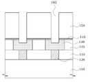
도 5를 참조하면, 제2 컨택플러그(140) 및 제2 층간절연막(125) 위에 식각 정지막(145)을 증착한다. 이 식각 정지막(145)은 이후 스토리지노드 컨택홀을 형성하는 과정에서 식각을 정지시키는 역할을 한다. 여기서 식각 정지막(145)은 산화막과 식각 선택비가 우수한 막으로 형성하며, 실리콘나이트라이드(Si3N4)막, 탄탈륨옥사이드(TaO2)막 또는 질화알루미늄(AlN)막으로 형성할 수 있다.Referring to FIG. 5, an
다음에 식각 정지막(145) 위에 스토리지노드 절연막(150)을 형성한다. 스토리지노드 절연막(150)은 캐패시터가 형성될 높이만큼 형성한다. 여기서 스토리지노드 절연막(150)은 화학기상증착법(CVD; Chemical Vapor Deposition)을 이용하여 PETEOS(Plasma Enhanced Tetra Ortho Ethyl Silicon) 산화막을 단일막으로 형성하거나, PSG(Phosphorus Silicon Glass)막과 TEOS 산화막의 이중막으로 형성할 수 있다. 그리고 스토리지노드 절연막(150) 위에 하드마스크막 및 반사방지막(ARC; Anti reflective coating)을 형성하고, 이 반사방지막 및 하드마스크막을 선택적으로 식각하여 스토리지노드 절연막(150)의 소정 영역을 노출시키는 하드마스크막 패턴(155) 및 반사방지막 패턴(160)을 형성한다.Next, a storage
도 6을 참조하면, 스토리지노드 절연막(150) 내에 1차 스토리지노드 컨택홀(165)을 형성한다. 구체적으로, 반사방지막 패턴(160) 및 하드마스크막 패턴(155)을 마스크로 노출된 스토리지노드 절연막(155)을 식각 정지막(145)이 노출 될 때까지 식각한다. 다음에 노출된 식각 정지막(145)도 식각하여 제2 컨택플러그(140)를 노출시키는 1차 스토리지노드 컨택홀(165)을 형성한다. 여기서 1차 스토리지노드 컨택홀(165)을 형성하기 위해 진행하는 식각 과정에서 제2 컨택플러그(140) 또한 소정 깊이만큼 식각될 수 있다. 그리고 반사방지막 패턴(160) 및 하드마스크막 패턴(155)은 제거한다.Referring to FIG. 6, a primary storage
도 7을 참조하면, 반도체 기판(105) 상에 세정 공정을 진행하여 제2 컨택플러그(140)를 매립하는 금속성 절연막을 식각한다. 구체적으로, 반도체 기판(105) 상에 암모니아(NH4)계 용액이 함유된 식각 용액을 공급한다. 여기서 암모니아(NH4)계 용액이 함유된 식각 용액은 수산화암모늄(NH4OH) 용액과 물(H2O)의 혼합용액 또는 수산화암모늄(NH4OH) 용액과 과산화수소(H2O2)의 혼합용액을 이용할 수 있다. 이때, 암모니아(NH4)계 용액이 함유된 식각 용액은 수산화암모늄(NH4OH), 물(H2O) 및 과산화수소(H2O2)가 혼합된 SC-1(Standard Chemical) 용액을 이용할 수도 있다. 여기서 SC-1 용액을 이용하여 제2 컨택플러그(140)를 식각하는 경우, 분당 26Å의 두께로 식각할 수 있다.Referring to FIG. 7, the metal insulating layer filling the
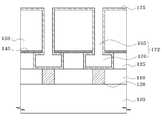
이와 같이 암모니아(NH4)계 용액이 함유된 식각 용액을 이용한 세정을 진행하면, 제2 컨택플러그(140)를 구성하는 금속성 절연막과 스토리지노드 절연막(150) 및 제2 층간절연막(125)을 구성하는 산화막간의 식각 선택비에 의해 주변 산화막에 손상 없이 제2 컨택플러그(140)를 매립하고 있는 금속성 절연막만을 선택적으로 제 거할 수 있다. 이와 같이, 제2 컨택플러그(140)를 매립하는 금속성 절연막을 제거하면, 1차 스토리지노드 컨택홀(165) 및 1차 스토리지노드 컨택홀(165)보다 내부 면적이 넓으면서 제1 컨택플러그(120) 및 제1 층간절연막(110)이 일부 노출되는 2차 스토리지노드 컨택홀(170) 및 로 이루어진 스토리지노드 컨택홀(172)이 형성된다.As such, when the cleaning process is performed using the etching solution containing the ammonia (NH4 ) solution, the metal insulating film, the storage
도 8을 참조하면, 스토리지노드 컨택홀(172) 및 스토리지노드 절연막(150) 위에 스토리지노드용 금속막(175)을 증착한다. 스토리지노드용 금속막(175)은 티타늄나이트라이드(TiN)막, 탄탈륨나이트라이드(TaN)막, 텅스텐나이트라이드(WN)막, 루테늄(Ru)막 및 플래티늄(Pt)막을 포함하는 그룹에서 하나 이상의 물질을 선택하여 형성할 수 있다.Referring to FIG. 8, a storage
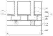
도 9를 참조하면, 스토리지노드용 금속막(175) 상에 분리 공정을 진행하여 스토리지노드용 절연막(150) 위의 스토리지노드용 금속막(175)을 제거한다. 그러면 스토리지노드 컨택홀(172) 내에 분리된 스토리지노드 전극(180)이 형성된다. 여기서 스토리지노용 금속막은 에치백(etchback) 또는 화학적기계적연마(CMP; Chemical Mechanical Polishing)방법을 이용하여 분리할 수 있다. 여기서 스토리지노드 전극(180)은 폭이 좁은 상부 부분(182)과 상부 부분(182)보다 상대적으로 폭이 넓은 하부 부분(184)을 포함하여 이루어진다.Referring to FIG. 9, a separation process is performed on the storage
도 10을 참조하면, 반도체 기판(105) 상에 딥-아웃(dip-out) 공정을 진행하여 스토리지노드 절연막(150)을 제거한다. 그러면 전극의 내측면 및 외측면이 모두 노출되는 실린더 타입(cylinder typed)의 스토리지노드 전극(180)이 형성된다. 여 기서 딥-아웃 공정은 산화막을 식각하는 습식식각용액을 이용하여 진행할 수 있다. 이때, 스토리지노드 전극(180)의 폭이 좁은 상부 부분(182)을 상기 상부 부분(182)보다 상대적으로 폭이 넓은 하부 부분(184)이 지지하는 역할을 하여 전극의 좁은 폭에 의해 유발되는 브릿지성 결함을 방지할 수 있다.Referring to FIG. 10, the storage
도 11을 참조하면, 스토리지노드 전극(180) 위에 유전체막(185) 및 플레이트 전극(190)을 형성한다. 여기서 유전체막(185)은 하프늄옥사이드(HfO2)를 포함하는 고유전체 물질을 유전체 박막 재료로 적용할 수 있다. 플레이트전극(190)은 스토리지노드 전극(180)과 대등한 물질, 예를 들어 티타늄나이트라이드(TiN)막, 탄탈륨나이트라이드(TaN)막, 텅스텐나이트라이드(WN)막, 루테늄(Ru)막 및 플래티늄(Pt)막을 포함하는 그룹에서 하나 이상의 물질을 선택하여 형성할 수 있다.Referring to FIG. 11, a
본 발명에 따른 반도체 소자의 캐패시터 형성방법은, 1차 스토리지노드 컨택홀 및 1차 스토리지노드 컨택홀보다 내부 면적이 넓은 2차 스토리지노드 컨택홀을 포함하는 스토리지노드 컨택홀을 형성하고, 스토리지노드 컨택홀 내에 스토리지노드 전극을 형성함으로써 스토리지노드 전극의 상부 보다 하부가 면적을 증가시킨다. 이에 따라 딥-아웃 프로세스를 이용한 실린더 구조의 스토리지노드 전극을 형성하는 과정에서 면적이 넓은 하부가 폭이 좁은 상부의 지지대 역할을 하여 스토리지노드 전극의 상부 부분이 휘어지는 리닝 현상에 의해 유발되는 브릿지성 결함을 방지할 수 있다.In the method of forming a capacitor of a semiconductor device according to the present invention, a storage node contact hole including a primary storage node contact hole and a secondary storage node contact hole having a larger inner area than the primary storage node contact hole is formed, and the storage node contact is formed. By forming the storage node electrode in the hole, the area of the lower portion than the upper portion of the storage node electrode increases. Accordingly, in the process of forming a storage node electrode having a cylindrical structure using a deep-out process, a bridge defect caused by a lining phenomenon in which an upper portion of the storage node electrode is bent as a lower portion having a large area serves as a support for a narrow upper portion. Can be prevented.
도 1은 스토리지노드전극을 상부에서 나타내보인 도면이다.1 is a view showing a storage node electrode from above.
도 2 내지 도 11은 반도체 소자의 캐패시터 형성방법을 설명하기 위해 나타내보인 도면들이다.2 through 11 are views for explaining a method of forming a capacitor of a semiconductor device.
Claims (7)
Translated fromKoreanPriority Applications (1)
| Application Number | Priority Date | Filing Date | Title |
|---|---|---|---|
| KR1020070109118AKR101003490B1 (en) | 2007-10-29 | 2007-10-29 | Capacitor Formation Method of Semiconductor Device |
Applications Claiming Priority (1)
| Application Number | Priority Date | Filing Date | Title |
|---|---|---|---|
| KR1020070109118AKR101003490B1 (en) | 2007-10-29 | 2007-10-29 | Capacitor Formation Method of Semiconductor Device |
Publications (2)
| Publication Number | Publication Date |
|---|---|
| KR20090043326A KR20090043326A (en) | 2009-05-06 |
| KR101003490B1true KR101003490B1 (en) | 2010-12-30 |
Family
ID=40854185
Family Applications (1)
| Application Number | Title | Priority Date | Filing Date |
|---|---|---|---|
| KR1020070109118AExpired - Fee RelatedKR101003490B1 (en) | 2007-10-29 | 2007-10-29 | Capacitor Formation Method of Semiconductor Device |
Country Status (1)
| Country | Link |
|---|---|
| KR (1) | KR101003490B1 (en) |
Families Citing this family (1)
| Publication number | Priority date | Publication date | Assignee | Title |
|---|---|---|---|---|
| KR101631165B1 (en) | 2009-12-14 | 2016-06-17 | 삼성전자주식회사 | Method Of Forming Semiconductor Cell Structure, Method Of Forming Semiconductor Device Comprising The Semiconductor Cell Structure, And Method Of Forming Semiconductor Module Comprising The Semiconductor Device |
Citations (4)
| Publication number | Priority date | Publication date | Assignee | Title |
|---|---|---|---|---|
| US6429087B2 (en) | 1999-08-30 | 2002-08-06 | Micron Technology, Inc. | Methods of forming capacitors |
| KR100388682B1 (en) | 2001-03-03 | 2003-06-25 | 삼성전자주식회사 | Storage electric terminal layer and method for forming thereof |
| KR100672816B1 (en) | 2004-03-16 | 2007-01-22 | 삼성전자주식회사 | Capacitor Formation Method of Semiconductor Memory Device |
| US7235452B2 (en) | 2003-03-05 | 2007-06-26 | Hynix Semiconductor Inc. | Method for fabricating capacitor in semiconductor device |
- 2007
- 2007-10-29KRKR1020070109118Apatent/KR101003490B1/ennot_activeExpired - Fee Related
Patent Citations (4)
| Publication number | Priority date | Publication date | Assignee | Title |
|---|---|---|---|---|
| US6429087B2 (en) | 1999-08-30 | 2002-08-06 | Micron Technology, Inc. | Methods of forming capacitors |
| KR100388682B1 (en) | 2001-03-03 | 2003-06-25 | 삼성전자주식회사 | Storage electric terminal layer and method for forming thereof |
| US7235452B2 (en) | 2003-03-05 | 2007-06-26 | Hynix Semiconductor Inc. | Method for fabricating capacitor in semiconductor device |
| KR100672816B1 (en) | 2004-03-16 | 2007-01-22 | 삼성전자주식회사 | Capacitor Formation Method of Semiconductor Memory Device |
Also Published As
| Publication number | Publication date |
|---|---|
| KR20090043326A (en) | 2009-05-06 |
Similar Documents
| Publication | Publication Date | Title |
|---|---|---|
| US7799631B2 (en) | Multiple-layer dielectric layer and method for fabricating capacitor including the same | |
| US8017491B2 (en) | Method for fabricating capacitor | |
| CN100490061C (en) | Method for fabricating capacitor in semiconductor device | |
| CN101587860A (en) | Method for fabricating semiconductor device | |
| US7531422B2 (en) | Method for fabricating capacitor in semiconductor device using hafnium terbium oxide dielectric layer | |
| JP2004214655A (en) | Capacitor having oxygen diffusion preventing film and method for manufacturing the same | |
| KR100418580B1 (en) | Method of forming a capacitor of a semiconductor device | |
| US7923343B2 (en) | Capacitor of semiconductor device and method for forming the same | |
| KR100464649B1 (en) | Capacitor of semiconductor device having dual dielectric layer structure and method for fabricating the same | |
| KR101003490B1 (en) | Capacitor Formation Method of Semiconductor Device | |
| US7547598B2 (en) | Method for fabricating capacitor in semiconductor device | |
| TW201937602A (en) | Dram and production method of same | |
| US7582525B2 (en) | Method for fabricating capacitor of semiconductor memory device using amorphous carbon | |
| US20100325853A1 (en) | Method for fabricating capacitor | |
| KR20040049659A (en) | A method for forming a capacitor of a semiconductor device | |
| US20060141699A1 (en) | Method for fabricating semiconductor memory device | |
| US7361598B2 (en) | Method for fabricating semiconductor device capable of preventing scratch | |
| CN100590845C (en) | Manufacturing method of capacitor in semiconductor device | |
| KR100811255B1 (en) | Capacitor Formation Method of Semiconductor Device | |
| KR100937988B1 (en) | Capacitor Manufacturing Method of Semiconductor Device | |
| KR100345065B1 (en) | Method for manufacturing capacitor in semiconductor device | |
| US7439150B2 (en) | Method of manufacturing a semiconductor device | |
| KR20030048883A (en) | A method for forming a capacitor of a semiconductor device | |
| KR100575883B1 (en) | Capacitor Formation Method of Semiconductor Device | |
| KR100683485B1 (en) | Capacitor Manufacturing Method of Semiconductor Device |
Legal Events
| Date | Code | Title | Description |
|---|---|---|---|
| PA0109 | Patent application | St.27 status event code:A-0-1-A10-A12-nap-PA0109 | |
| A201 | Request for examination | ||
| PA0201 | Request for examination | St.27 status event code:A-1-2-D10-D11-exm-PA0201 | |
| PG1501 | Laying open of application | St.27 status event code:A-1-1-Q10-Q12-nap-PG1501 | |
| D13-X000 | Search requested | St.27 status event code:A-1-2-D10-D13-srh-X000 | |
| D14-X000 | Search report completed | St.27 status event code:A-1-2-D10-D14-srh-X000 | |
| E701 | Decision to grant or registration of patent right | ||
| PE0701 | Decision of registration | St.27 status event code:A-1-2-D10-D22-exm-PE0701 | |
| GRNT | Written decision to grant | ||
| PR0701 | Registration of establishment | St.27 status event code:A-2-4-F10-F11-exm-PR0701 | |
| PR1002 | Payment of registration fee | St.27 status event code:A-2-2-U10-U11-oth-PR1002 Fee payment year number:1 | |
| PG1601 | Publication of registration | St.27 status event code:A-4-4-Q10-Q13-nap-PG1601 | |
| PN2301 | Change of applicant | St.27 status event code:A-5-5-R10-R13-asn-PN2301 St.27 status event code:A-5-5-R10-R11-asn-PN2301 | |
| PN2301 | Change of applicant | St.27 status event code:A-5-5-R10-R13-asn-PN2301 St.27 status event code:A-5-5-R10-R11-asn-PN2301 | |
| LAPS | Lapse due to unpaid annual fee | ||
| PC1903 | Unpaid annual fee | St.27 status event code:A-4-4-U10-U13-oth-PC1903 Not in force date:20131217 Payment event data comment text:Termination Category : DEFAULT_OF_REGISTRATION_FEE | |
| PC1903 | Unpaid annual fee | St.27 status event code:N-4-6-H10-H13-oth-PC1903 Ip right cessation event data comment text:Termination Category : DEFAULT_OF_REGISTRATION_FEE Not in force date:20131217 | |
| PN2301 | Change of applicant | St.27 status event code:A-5-5-R10-R13-asn-PN2301 St.27 status event code:A-5-5-R10-R11-asn-PN2301 | |
| P22-X000 | Classification modified | St.27 status event code:A-4-4-P10-P22-nap-X000 | |
| P22-X000 | Classification modified | St.27 status event code:A-4-4-P10-P22-nap-X000 | |
| P22-X000 | Classification modified | St.27 status event code:A-4-4-P10-P22-nap-X000 | |
| P22-X000 | Classification modified | St.27 status event code:A-4-4-P10-P22-nap-X000 |