KR101002347B1 - Horizontal field applied thin film transistor substrate and manufacturing method thereof - Google Patents
Horizontal field applied thin film transistor substrate and manufacturing method thereofDownload PDFInfo
- Publication number
- KR101002347B1 KR101002347B1KR1020040047574AKR20040047574AKR101002347B1KR 101002347 B1KR101002347 B1KR 101002347B1KR 1020040047574 AKR1020040047574 AKR 1020040047574AKR 20040047574 AKR20040047574 AKR 20040047574AKR 101002347 B1KR101002347 B1KR 101002347B1
- Authority
- KR
- South Korea
- Prior art keywords
- common
- electrode
- gate
- line
- forming
- Prior art date
- Legal status (The legal status is an assumption and is not a legal conclusion. Google has not performed a legal analysis and makes no representation as to the accuracy of the status listed.)
- Expired - Lifetime
Links
Images


Classifications
- H—ELECTRICITY
- H10—SEMICONDUCTOR DEVICES; ELECTRIC SOLID-STATE DEVICES NOT OTHERWISE PROVIDED FOR
- H10D—INORGANIC ELECTRIC SEMICONDUCTOR DEVICES
- H10D86/00—Integrated devices formed in or on insulating or conducting substrates, e.g. formed in silicon-on-insulator [SOI] substrates or on stainless steel or glass substrates
- H10D86/01—Manufacture or treatment
- H10D86/021—Manufacture or treatment of multiple TFTs
- H10D86/0231—Manufacture or treatment of multiple TFTs using masks, e.g. half-tone masks
- H—ELECTRICITY
- H10—SEMICONDUCTOR DEVICES; ELECTRIC SOLID-STATE DEVICES NOT OTHERWISE PROVIDED FOR
- H10D—INORGANIC ELECTRIC SEMICONDUCTOR DEVICES
- H10D86/00—Integrated devices formed in or on insulating or conducting substrates, e.g. formed in silicon-on-insulator [SOI] substrates or on stainless steel or glass substrates
- H10D86/40—Integrated devices formed in or on insulating or conducting substrates, e.g. formed in silicon-on-insulator [SOI] substrates or on stainless steel or glass substrates characterised by multiple TFTs
- H10D86/441—Interconnections, e.g. scanning lines
- H—ELECTRICITY
- H10—SEMICONDUCTOR DEVICES; ELECTRIC SOLID-STATE DEVICES NOT OTHERWISE PROVIDED FOR
- H10D—INORGANIC ELECTRIC SEMICONDUCTOR DEVICES
- H10D86/00—Integrated devices formed in or on insulating or conducting substrates, e.g. formed in silicon-on-insulator [SOI] substrates or on stainless steel or glass substrates
- H10D86/40—Integrated devices formed in or on insulating or conducting substrates, e.g. formed in silicon-on-insulator [SOI] substrates or on stainless steel or glass substrates characterised by multiple TFTs
- H10D86/481—Integrated devices formed in or on insulating or conducting substrates, e.g. formed in silicon-on-insulator [SOI] substrates or on stainless steel or glass substrates characterised by multiple TFTs integrated with passive devices, e.g. auxiliary capacitors
- H—ELECTRICITY
- H10—SEMICONDUCTOR DEVICES; ELECTRIC SOLID-STATE DEVICES NOT OTHERWISE PROVIDED FOR
- H10D—INORGANIC ELECTRIC SEMICONDUCTOR DEVICES
- H10D86/00—Integrated devices formed in or on insulating or conducting substrates, e.g. formed in silicon-on-insulator [SOI] substrates or on stainless steel or glass substrates
- H10D86/40—Integrated devices formed in or on insulating or conducting substrates, e.g. formed in silicon-on-insulator [SOI] substrates or on stainless steel or glass substrates characterised by multiple TFTs
- H10D86/60—Integrated devices formed in or on insulating or conducting substrates, e.g. formed in silicon-on-insulator [SOI] substrates or on stainless steel or glass substrates characterised by multiple TFTs wherein the TFTs are in active matrices
- H—ELECTRICITY
- H10—SEMICONDUCTOR DEVICES; ELECTRIC SOLID-STATE DEVICES NOT OTHERWISE PROVIDED FOR
- H10D—INORGANIC ELECTRIC SEMICONDUCTOR DEVICES
- H10D86/00—Integrated devices formed in or on insulating or conducting substrates, e.g. formed in silicon-on-insulator [SOI] substrates or on stainless steel or glass substrates
- H10D86/80—Integrated devices formed in or on insulating or conducting substrates, e.g. formed in silicon-on-insulator [SOI] substrates or on stainless steel or glass substrates characterised by multiple passive components, e.g. resistors, capacitors or inductors
Landscapes
- Liquid Crystal (AREA)
Abstract
Translated fromKoreanDescription
Translated fromKorean도 1은 종래의 수평 전계 인가형 박막 트랜지스터 기판을 도시한 평면도.1 is a plan view showing a conventional horizontal field applied thin film transistor substrate.
도 2는 도 1에 도시된 박막 트랜지스터 기판을 Ⅰ-Ⅰ', Ⅱ-Ⅱ'선을 따라 절단하여 도시한 단면도.FIG. 2 is a cross-sectional view of the thin film transistor substrate illustrated in FIG. 1 taken along lines II ′ and II-II ′.
도 3a 내지 도 3d는 도 2에 도시된 박막 트랜지스터 기판의 제조 방법을 단계적으로 도시한 단면도들.3A to 3D are cross-sectional views sequentially illustrating a method of manufacturing the thin film transistor substrate illustrated in FIG. 2.
도 4는 본 발명의 실시 예에 따른 수평 전계 인가형 박막 트랜지스터 기판을 도시한 평면도.4 is a plan view illustrating a horizontal field applied thin film transistor substrate according to an exemplary embodiment of the present invention.
도 5는 도 4에 도시된 박막 트랜지스터 기판을 Ⅲ-Ⅲ', Ⅳ-Ⅳ', Ⅴ-Ⅴ', Ⅵ-Ⅵ'선을 따라 절단하여 도시한 단면도.FIG. 5 is a cross-sectional view of the thin film transistor substrate of FIG. 4 taken along lines III-III ', IV-IV', V-V ', and VI-VI'.
도 6a 및 도 6b는 본 발명의 실시 예에 따른 박막 트랜지스터 기판의 제조 방법 중 제1 마스크 공정을 설명하기 위한 평면도 및 단면도.6A and 6B are plan and cross-sectional views illustrating a first mask process in a method of manufacturing a thin film transistor substrate according to an exemplary embodiment of the present invention.
도 7a 내지 도 7e는 본 발명의 제1 마스크 공정을 구체적으로 설명하기 위한 단면도들.7A to 7E are cross-sectional views illustrating in detail the first mask process of the present invention.
도 8a 및 도 8b는 본 발명의 실시 예에 따른 박막 트랜지스터 기판의 제조 방법 중 제2 마스크 공정을 설명하기 위한 평면도 및 단면도.8A and 8B are plan and cross-sectional views illustrating a second mask process in a method of manufacturing a thin film transistor substrate according to an exemplary embodiment of the present invention.
도 9a 내지 도 9e는 본 발명의 제2 마스크 공정을 구체적으로 설명하기 위한 단면도들.9A to 9E are cross-sectional views for describing a second mask process of the present invention in detail.
도 10a 및 도 10b는 본 발명의 실시 예에 따른 박막 트랜지스터 기판의 제조 방법 중 제3 마스크 공정을 설명하기 위한 평면도 및 단면도.10A and 10B are a plan view and a cross-sectional view for describing a third mask process in the method of manufacturing the thin film transistor substrate according to the embodiment of the present invention.
도 11a 내지 도 11d는 본 발명의 실시 예에 따른 박막 트랜지스터 기판의 제조 방법 중 제4 마스크 공정을 설명하기 위한 평면도 및 단면도.11A to 11D are plan and cross-sectional views illustrating a fourth mask process in a method of manufacturing a thin film transistor substrate according to an exemplary embodiment of the present invention.
도 12는 본 발명의 다른 실시 예에 따른 수평 전계 인가형 박막 트랜지스터 기판을 도시한 단면도.12 is a cross-sectional view illustrating a horizontal field applied thin film transistor substrate according to another embodiment of the present invention.
도 13은 본 발명의 또 다른 실시 예에 따른 수평 전계 인가형 박막 트랜지스터 기판을 도시한 평면도.13 is a plan view illustrating a horizontal field applied thin film transistor substrate according to still another embodiment of the present invention.
도 14는 도 13에 도시된 박막 트랜지스터 기판을 Ⅲ-Ⅲ', Ⅳ-Ⅳ', Ⅴ-Ⅴ', Ⅵ-Ⅵ', Ⅶ-Ⅶ'선을 따라 절단하여 도시한 단면도.FIG. 14 is a cross-sectional view of the thin film transistor substrate of FIG. 13 taken along lines III-III ', IV-IV', V-V ', VI-VI', and VIII-VIII ';
< 도면의 주요 부분에 대한 부호의 설명 ><Description of Symbols for Main Parts of Drawings>
2, 102 : 게이트 라인 4, 104 : 데이터 라인2, 102:
6, TFT : 박막 트랜지스터 8 : 게이트 전극6, TFT: thin film transistor 8: gate electrode
10, 110 : 소스 전극 12, 112 : 드레인 전극10, 110:
13, 21, 27, 33, 39, 108, 128, 136, 144 : 컨택홀13, 21, 27, 33, 39, 108, 128, 136, 144: contact hole
14, 118 : 화소 전극14, 118: pixel electrode
16, 120 : 공통 라인 18, 122, 222 : 공통 전극16, 120:
20, Cst1, Cst2 : 스토리지 캐패시터 22 : 스토리지 상부 전극20, Cst1, Cst2: storage capacitor 22: storage upper electrode
24, 124 : 게이트 패드 26, 126 : 게이트 패드 하부 전극24, 124:
28, 130 : 게이트 패드 상부 전극 30, 132 : 데이터 패드28 and 130: gate pad
32, 134 : 데이터 패드 하부 전극 34, 138 : 데이터 패드 상부 전극32, 134: data pad
36, 140 : 공통 패드 38, 142 : 공통 패드 하부 전극36, 140:
146 : 공통 패드 상부 전극 45, 150 : 기판146: common pad
46, 152 : 게이트 절연막 48, 114 : 활성층46, 152: gate
50, 116 : 오믹접촉층 52, 154 : 보호막50, 116:
101 : 제1 도전층 103 : 제2 도전층101: first conductive layer 103: second conductive layer
105 : 비정질 실리콘층 107 : 불순물 도핑된 실리콘층105: amorphous silicon layer 107: impurity doped silicon layer
109 : 소스/드레인 금속층 118A, 118C : 화소 전극 수평부109: source /
118B : 화소 전극 핑거부 122A, 222A : 공통 전극 수평부118B: pixel
122B, 222B : 공통 전극 핑거부 160 : 하프 톤 마스크122B and 222B: common electrode finger portion 160: halftone mask
166, 172 : 석영 기판 162, 174 : 차단부166, 172:
162 : 부분 투과부 167, 180 : 포토레지스트162:
168, 182 : 포토레지스터 패턴 168A, 182A : 제1 포토레지스트 패턴168 and 182:
168B, 182B : 제2 포토레지스트 패턴
168B, 182B: second photoresist pattern
본 발명은 수평 전계를 이용하는 액정 표시 장치에 관한 것으로, 특히 공정을 단순화할 수 있는 수평 전계 인가형 박막 트랜지스터 기판 및 그 제조 방법에 관한 것이다.BACKGROUND OF THE INVENTION 1. Field of the Invention The present invention relates to a liquid crystal display device using a horizontal electric field, and more particularly, to a horizontal field applied thin film transistor substrate and a method of manufacturing the same, which can simplify the process.
액정 표시 장치는 전계를 이용하여 액정의 광투과율을 조절함으로써 화상을 표시하게 된다. 이러한 액정 표시 장치는 액정을 구동시키는 전계의 방향에 따라 수직 전계 인가형과 수평 전계 인가형으로 대별된다.The liquid crystal display device displays an image by adjusting the light transmittance of the liquid crystal using an electric field. Such liquid crystal displays are roughly classified into a vertical electric field application type and a horizontal electric field application type according to the direction of the electric field for driving the liquid crystal.
수직 전계 인가형 액정 표시 장치는 상하부 기판에 대향하게 배치된 화소 전극과 공통 전극 사이에 형성되는 수직 전계에 의해 TN(Twisted Nemastic) 모드의 액정을 구동하게 된다. 이러한 수직 전계 인가형 액정 표시 장치는 개구율이 큰 장점을 가지는 반면 시야각이 90도 정도로 좁은 단점을 가진다.In the vertical field applying liquid crystal display, a liquid crystal of TN (Twisted Nemastic) mode is driven by a vertical electric field formed between a pixel electrode and a common electrode disposed to face the upper and lower substrates. The vertical field application type liquid crystal display device has an advantage of having a large aperture ratio while having a narrow viewing angle of about 90 degrees.
수평 전계 인가형 액정 표시 장치는 하부 기판에 나란하게 배치된 화소 전극과 공통 전극 간의 수평 전계에 의해 인 플레인 스위칭(In Plane Switching; 이하, IPS라 함) 모드의 액정을 구동하게 된다. 이러한 수평 전계 인가형 액정 표시 장치는 시야각이 160도 정도로 넓은 장점을 가진다. 이하, 수평 전계 인가형 액정 표시 장치에 대하여 상세히 살펴보기로 한다.The horizontal field application type liquid crystal display drives liquid crystal in In Plane Switching (IPS) mode by a horizontal electric field between a pixel electrode and a common electrode disposed side by side on a lower substrate. Such a horizontal field application liquid crystal display device has an advantage that a viewing angle is about 160 degrees. Hereinafter, the horizontal field application liquid crystal display will be described in detail.
수평 전계 인가형 액정 표시 장치는 서로 대향하여 합착된 박막 트랜지스터 기판(하판) 및 칼러 필터 기판(상판)과, 두 기판 사이에서 셀갭을 일정하게 유지시키기 위한 스페이서와, 그 셀갭에 채워진 액정을 구비한다.The horizontal field application type liquid crystal display device includes a thin film transistor substrate (bottom plate) and a color filter substrate (top plate) bonded to each other, a spacer for keeping a cell gap constant between the two substrates, and a liquid crystal filled in the cell gap. .
박막 트랜지스터 기판은 화소 단위의 수평 전계 형성을 위한 다수의 신호 배선들 및 박막 트랜지스터와, 그들 위에 액정 배향을 위해 도포된 배향막으로 구성된다. 칼라 필터 기판은 칼러 구현을 위한 칼라 필터 및 빛샘 방지를 위한 블랙 매트릭스와, 그들 위에 액정 배향을 위해 도포된 배향막으로 구성된다.The thin film transistor substrate is composed of a plurality of signal lines and a thin film transistor for forming a horizontal electric field in pixels, and an alignment film coated thereon for liquid crystal alignment. The color filter substrate is composed of a color filter for color implementation and a black matrix for light leakage prevention, and an alignment film coated thereon for liquid crystal alignment.
이러한 액정 표시 장치에서 박막 트랜지스터 기판은 반도체 공정을 포함함과 아울러 다수의 마스크 공정을 필요로 함에 따라 제조 공정이 복잡하여 액정 패널 제조 단가 상승의 중요 원인이 되고 있다. 이를 해결하기 위하여, 박막 트랜지스터 기판은 마스크 공정수를 줄이는 방향으로 발전하고 있다. 이는 하나의 마스크 공정이 박막 증착 공정, 세정 공정, 포토리소그래피 공정, 식각 공정, 포토레지스트 박리 공정, 검사 공정 등과 같은 많은 공정을 포함하고 있기 때문이다. 이에 따라, 최근에는 박막 트랜지스터 기판의 표준 마스크 공정이던 5 마스크 공정에서 하나의 마스크 공정을 줄인 4 마스크 공정이 대두되고 있다.In such a liquid crystal display device, the thin film transistor substrate includes a semiconductor process and requires a plurality of mask processes, and thus, the manufacturing process is complicated, which is an important cause of an increase in the manufacturing cost of the liquid crystal panel. In order to solve this problem, the thin film transistor substrate is developing in a direction of reducing the number of mask processes. This is because one mask process includes many processes such as a thin film deposition process, a cleaning process, a photolithography process, an etching process, a photoresist stripping process, an inspection process, and the like. Accordingly, in recent years, a four-mask process that reduces one mask process has emerged in the five-mask process, which is a standard mask process of a thin film transistor substrate.
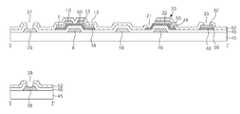
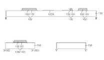
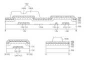
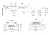
도 1은 종래의 4마스크 공정을 이용한 수평 전계 인가형 박막 트랜지스터 기판을 도시한 평면도이고, 도 2는 도 1에 도시된 박막 트랜지스터 기판을 Ⅰ-Ⅰ', Ⅱ-Ⅱ'선을 따라 절단하여 도시한 단면도이다.FIG. 1 is a plan view showing a horizontal field applied thin film transistor substrate using a conventional four mask process, and FIG. 2 is a cutaway view of the thin film transistor substrate shown in FIG. 1 along lines I-I 'and II-II'. One cross section.
도 1 및 도 2에 도시된 박막 트랜지스터 기판은 하부 기판(45) 위에 게이트 절연막(46)을 사이에 두고 교차하게 형성된 게이트 라인(2) 및 데이터 라인(4)과, 그 교차부마다 형성된 박막 트랜지스터(6)와, 그 교차 구조로 마련된 화소 영역에 수평 전계를 형성하도록 형성된 화소 전극(14) 및 공통 전극(18)과, 공통 전극(18)과 접속된 공통 라인(16)을 구비한다. 그리고, 박막 트랜지스터 기판은 화소 전극 (14)과 공통 전극 라인(16)의 중첩부에 형성된 스토리지 캐패시터(20)와, 게이트 라인(2)과 접속된 게이트 패드(24)와, 데이터 라인(4)과 접속된 데이터 패드(30)와, 공통 라인(16)과 접속된 공통 패드(36)를 추가로 구비한다.The thin film transistor substrate illustrated in FIGS. 1 and 2 includes a
게이트 신호를 공급하는 게이트 라인(2)과 데이터 신호를 공급하는 데이터 라인(4)은 교차 구조로 형성되어 화소 영역을 정의한다.The
액정 구동을 위한 기준 전압을 공급하는 공통 라인(16)은 화소 영역을 사이에 두고 게이트 라인(2)과 나란하게 형성된다.The
박막 트랜지스터(6)는 게이트 라인(2)의 게이트 신호에 응답하여 데이터 라인(4)의 화소 신호가 화소 전극(14)에 충전되어 유지되게 한다. 이를 위하여, 박막 트랜지스터(6)는 게이트 라인(2)과 접속된 게이트 전극(8), 데이터 라인(4)과 접속된 소스 전극(10), 화소 전극(14)과 접속된 드레인 전극(12), 게이트 전극(8)과 게이트 절연막(46)을 사이에 두고 중첩되면서 소스 전극(10) 및 드레인 전극(12) 사이에 채널을 형성하는 활성층(48), 소스 전극(10) 및 드레인 전극(12)과 활성층(48)과의 오믹 접촉을 위한 오믹 컨택층(50)을 구비한다.The
그리고, 활성층(48) 및 오믹 컨택층(50)은 데이터 라인(4), 데이터 패드 하부 전극(32), 그리고 스토리지 상부 전극(22)과도 중첩되게 형성된다.The
화소 전극(14)은 보호막(52)을 관통하는 제1 컨택홀(13)을 통해 박막 트랜지스터(6)의 드레인 전극(12)과 접속되어 화소 영역에 형성된다. 이러한 화소 전극(14)은 드레인 전극(12)과 접속되고 인접한 게이트 라인(2)과 나란하게 형성된 제1 수평부(14A)와, 공통 라인(16)과 중첩되게 형성된 제2 수평부(14B)와, 제1 및 제2 수평부(14A, 14B) 사이에 나란하게 형성된 핑거부(14C)를 구비한다.The
공통 전극(18)은 공통 라인(16)과 접속되어 화소 영역에 형성된다. 이러한 공통 전극(18)은 화소 영역(5)에서 화소 전극(14)의 핑거부(14C)와 나란하게 형성된다.The
이에 따라, 박막 트랜지스터(6)를 통해 화소 신호가 공급된 화소 전극(14)과 공통 라인(16)을 통해 기준 전압(이하, 공통 전압)이 공급된 공통 전극(18) 사이에는 수평 전계가 형성된다. 특히, 화소 전극(14)의 핑거부(14C)와 공통 전극(18) 사이에 수평 전계가 형성된다. 이러한 수평 전계에 의해 박막 트랜지스터 기판과 칼라 필터 기판 사이에서 수평 방향으로 배열된 액정 분자들이 유전 이방성에 의해 회전하게 된다. 그리고, 액정 분자들의 회전 정도에 따라 화소 영역을 투과하는 광 투과율이 달라지게 됨으로써 계조를 구현하게 된다.Accordingly, a horizontal electric field is formed between the
스토리지 캐패시터(20)는 공통 라인(16)과, 그 공통 라인(16)과 게이트 절연막(46), 활성층(48), 오믹 컨택층(50)을 사이에 두고 중첩되고 보호막(50)에 형성된 제2 컨택홀(21)을 통해 화소 전극(14)과 접속된 스토리지 상부 전극(22)으로 구성된다. 이러한 스토리지 캐패시터(20)는 화소 전극(14)에 충전된 화소 신호가 다음 화소 신호가 충전될 때까지 안정적으로 유지되게 한다.The
게이트 라인(2)은 게이트 패드(24)를 통해 게이트 드라이버(미도시)와 접속된다. 게이트 패드(24)는 게이트 라인(2)으로부터 연장된 게이트 패드 하부 전극(26)과, 게이트 절연막(46) 및 보호막(52)을 관통하는 제3 컨택홀(27)을 통해 게이트 패드 하부 전극(26)과 접속된 게이트 패드 상부 전극(28)으로 구성된다.The
데이터 라인(4)은 데이터 패드(30)를 통해 데이터 드라이버(미도시)와 접속된다. 데이터 패드(30)는 데이터 라인(4)으로부터 연장된 데이터 패드 하부 전극(32)과, 보호막(52)을 관통하는 제4 컨택홀(33)을 통해 데이터 패드 하부 전극(32)과 접속된 데이터 패드 상부 전극(34)으로 구성된다.The
공통 라인(16)은 공통 패드(36)를 통해 외부의 공통 전압원(미도시)으로부터 공통 전압을 공급받게 된다. 공통 패드(36)는 공통 라인(16)으로부터 연장된 공통 패드 하부 전극(38)과, 게이트 절연막(46) 및 보호막(52)을 관통하는 제5 컨택홀(39)을 통해 공통 패드 하부 전극(38)과 접속된 공통 패드 상부 전극(40)으로 구성된다.The
이러한 구성을 가지는 박막 트랜지스터 기판의 제조 방법을 4마스크 공정을 이용하여 상세히 하면 도 3a 내지 도 3d에 도시된 바와 같다.A method of manufacturing a thin film transistor substrate having such a configuration will be described with reference to FIGS. 3A to 3D in detail using a four mask process.
도 3a를 참조하면, 제1 마스크 공정을 이용하여 하부 기판(45) 상에 게이트 라인(2), 게이트 전극(8), 게이트 패드 하부 전극(26), 공통 라인(16), 공통 전극(18), 공통 패드 하부 전극(38)을 포함하는 게이트 금속 패턴이 형성된다.Referring to FIG. 3A, the
상세히 하면, 하부 기판(45) 상에 스퍼터링 방법 등의 증착 방법을 통해 게이트 금속층이 형성된다. 이어서, 제1 마스크를 이용한 포토리소그래피 공정과 식각 공정으로 게이트 금속층이 패터닝됨으로써 게이트 라인(2), 게이트 전극(8), 게이트 패드 하부 전극(26), 공통 라인(16), 공통 전극(18), 공통 패드 하부 전극(38)을 포함하는 게이트 금속 패턴이 형성된다. 게이트 금속층으로는 Al, Mo, Cr계 등의 금속이 단일층 또는 이중층 구조로 이용된다.In detail, the gate metal layer is formed on the
도 3b를 참조하면, 게이트 금속 패턴이 형성된 하부 기판(45) 상에 게이트 절연막(46)이 도포된다. 그리고 제2 마스크 공정을 이용하여 게이트 절연막(46) 위에 활성층(48) 및 오믹 컨택층(50)을 포함하는 반도체 패턴과; 데이터 라인(4), 소스 전극(10), 드레인 전극(12), 데이터 패드 하부 전극(32), 스토리지 상부 전극(22)을 포함하는 소스/드레인 금속 패턴이 형성된다.Referring to FIG. 3B, a
상세히 하면, 게이트 금속 패턴이 형성된 하부 기판(45) 상에 PECVD, 스퍼터링 등의 증착 방법을 통해 게이트 절연막(46), 비정질 실리콘층, n+ 비정질 실리콘층, 그리고 소스/드레인 금속층이 순차적으로 형성된다. 여기서, 게이트 절연막(46)의 재료로는 SiOx, SiNx 등의 무기 절연 물질이 이용된다. 소스/드레인 금속층으로는 Al, Mo, Cr계 등의 금속이 단일층 또는 이중층 구조로 이용된다. 그 다음, 소스/드레인 금속층 위에 제2 마스크를 이용한 포토리소그래피 공정으로 단차를 갖는 포토레지스트 패턴을 형성하게 된다. 단차를 갖는 포토레지스트 패턴을 이용한 습식 식각 공정으로 소스/드레인 금속층이 패터닝됨으로써 데이터 라인(4), 소스 전극(10), 그 소스 전극(10)과 일체화된 드레인 전극(12), 스토리지 상부 전극(22)을 포함하는 소스/드레인 금속 패턴이 형성된다. 그리고, 동일한 포토레지스트 패턴을 이용한 건식 식각 공정으로 n+ 비정질 실리콘층과 비정질 실리콘층이 동시에 패터닝됨으로써 오믹 컨택층(50)과 활성층(48)이 형성된다. 이어서, 포토레지스트 패턴을 애싱하고 노출된 소스/드레인 금속 패턴을 오믹 컨택층(50)과 함께 식각함으로써 소스 전극(10) 및 드레인 전극(12)이 분리된다.In detail, the
그 다음, 스트립 공정으로 소스/드레인 금속 패턴 위에 남아 있던 포토레지 스트 패턴이 제거된다.The stripping process then removes the photoresist pattern remaining on the source / drain metal pattern.
도 3c를 참조하면, 소스/드레인 금속 패턴이 형성된 게이트 절연막(46) 상에 제3 마스크 공정을 이용하여 제1 내지 제5 콘택홀들(13, 21, 27, 33, 39)을 포함하는 보호막(52)이 형성된다.Referring to FIG. 3C, a passivation layer including first to fifth contact holes 13, 21, 27, 33, and 39 on the
상세히 하면, 소스/드레인 금속 패턴이 형성된 게이트 절연막(46) 상에 PECVD 등의 증착 방법으로 보호막(52)이 전면 형성된다. 이어서, 보호막(52)이 제3 마스크를 이용한 포토리소그래피 공정과 식각 공정으로 패터닝됨으로써 제1 내지 제5 컨택홀들(13, 21, 27, 33, 39)이 형성된다. 제1 컨택홀(13)은 보호막(52)을 관통하여 드레인 전극(12)을, 제2 컨택홀(21)은 보호막(52)을 관통하여 스토리지 상부 전극(22)을 노출시킨다. 제3 컨택홀(27)은 보호막(52) 및 게이트 절연막(46)을 관통하여 게이트 패드 하부 전극(26)을, 제4 컨택홀(33)은 보호막(52)을 관통하여 데이터 패드 하부 전극(32)을, 제5 컨택홀(39)은 보호막(52) 및 게이트 절연막(46)을 관통하여 공통 패드 하부 전극(38)을 노출시킨다.In detail, the
여기서, 보호막(52)의 재료로는 게이트 절연막(46)과 같은 무기 절연 물질이나 유전상수가 작은 아크릴(acryl)계 유기 화합물, BCB 또는 PFCB 등과 같은 유기 절연 물질이 이용된다.As the material of the
도 3d를 참조하면, 제4 마스크 공정을 이용하여 보호막(52) 상에 화소 전극(14), 게이트 패드 상부 전극(28), 데이터 패드 상부 전극(34), 공통 패드 상부 전극(40)을 포함하는 투명 도전 패턴이 형성된다.Referring to FIG. 3D, the
상세히 하면, 보호막(52) 상에 스퍼터링 등의 증착 방법으로 투명 도전막이 도포된다. 이어서 제4 마스크를 이용한 포토리소그래피 공정과 식각 공정을 통해 투명 도전막이 패텅님됨으로써 화소 전극(14), 게이트 패드 상부 전극(28), 데이터 패드 상부 전극(34), 공통 패드 상부 전극(40)을 포함하는 투명 도전 패턴이 형성된다. 화소 전극(14)은 제1 컨택홀(13)을 통해 노출된 드레인 전극(12)과 접속되고, 제2 컨택홀(21)을 통해 노출된 스토리지 상부 전극(22)과 접속된다. 게이트 패드 상부 전극(28)은 제3 컨택홀(37)을 통해 노출된 게이트 패드 하부 전극(26)과 접속된다. 데이터 패드 상부 전극(34)은 제4 컨택홀(33)을 통해 노출된 데이터 하부 전극(32)과 접속된다. 공통 패드 상부 전극(40)은 제5 컨택홀(39)을 통해 노출된 공통 패드 하부 전극(38)과 접속된다.In detail, the transparent conductive film is apply | coated on the
여기서, 투명 도전막의 재료로는 ITO(Indium Tin Oxide) 등이 이용된다.Here, indium tin oxide (ITO) or the like is used as a material of the transparent conductive film.
이와 같이, 종래의 수평 전계 인가형 박막 트랜지스터 기판 및 그 제조 방법은 4마스크 공정으로 공정수를 줄임으로써 그에 비례하는 제조 단가를 절감할 수 있게 된다.As described above, the conventional horizontal field-applied thin film transistor substrate and its manufacturing method can reduce the manufacturing cost in proportion to the number of processes in a four mask process.
그러나, 화소 영역에 형성된 공통 전극(18)이 불투명한 게이트 금속으로 형성됨에 따라 개구율이 낮은 문제점이 있다.However, as the
또한, 개구율 문제로 인하여 불투명한 금속으로 이루어진 공통 라인(16)과 스토리지 상부 전극(22)과의 중첩 면적을 증가시키는데 한계가 있으므로 스토리지 캐패시터(20) 용량이 작은 문제점이 있다.
In addition, the
따라서, 본 발명의 목적은 공정을 단순화하면서도 개구율을 증가시킬 수 있는 수평 전계 인가형 박막 트랜지스터 기판 및 그 제조 방법을 제공하는 것이다. Accordingly, it is an object of the present invention to provide a horizontal field applied thin film transistor substrate capable of increasing the aperture ratio while simplifying the process, and a method of manufacturing the same.
본 발명의 다른 목적은 개구율 감소 없이 스토리지 캐패시터의 용량을 증가시킬 수 있는 수평 전계 인가형 박막 트랜지스터 기판 및 그 제조 방법을 제공하는 것이다.
Another object of the present invention is to provide a horizontal field applied thin film transistor substrate capable of increasing the capacity of a storage capacitor without reducing the aperture ratio, and a method of manufacturing the same.
상기 목적을 달성하기 위하여, 본 발명의 실시 예에 따른 수평 전계 인가형 박막 트랜지스터 기판은 투명한 제1 도전층과 불투명한 제2 도전층이 적층된 이중 구조의 게이트 라인과; 상기 게이트 라인과 절연되면서 교차하여 화소 영역을 정의하는 데이터 라인과; 상기 게이트 라인 및 데이터 라인과 접속된 박막 트랜지스터와; 상기 게이트 라인과 나란하며 상기 이중 구조로 형성된 공통 라인과; 상기 화소 영역에 상기 공통 라인의 제1 도전층이 연장되어 형성된 공통 전극과; 상기 박막 트랜지스터와 접속되고 상기 화소 영역에 상기 공통 전극과 수평 전계를 형성하기 위하여 형성된 화소 전극을 구비한다.In order to achieve the above object, the horizontal field-applied thin film transistor substrate according to an embodiment of the present invention includes a gate line of a dual structure in which a transparent first conductive layer and an opaque second conductive layer is stacked; A data line insulated from and intersecting the gate line to define a pixel area; A thin film transistor connected to the gate line and the data line; A common line parallel to the gate line and formed of the double structure; A common electrode formed by extending a first conductive layer of the common line in the pixel region; And a pixel electrode connected to the thin film transistor and formed to form a horizontal electric field with the common electrode in the pixel region.
그리고, 본 발명의 실시 예에 따른 수평 전계 인가형 박막 트랜지스터 기판의 제조 방법은 제1 마스크를 이용하여 기판 상에 투명한 제1 도전층 및 불투명한 제2 도전층이 적층된 이중 구조의 게이트 패턴과, 그 이중 구조의 공통 라인 및 상기 제1 도전층으로 이루어진 공통 전극을 포함하는 공통 패턴을 형성하는 단계와; 상기 게이트 패턴 및 공통 패턴을 덮는 게이트 절연막을 형성하는 단계와; 제2 마 스크를 이용하여 상기 게이트 절연막 상에 반도체 패턴과, 그 위에 중첩된 데이터 라인 및 소스 전극과 드레인 전극을 포함하는 소스/드레인 패턴을 형성하는 단계와; 상기 소스/드레인 패턴을 덮는 보호막을 형성하고 제3 마스크를 이용하여 상기 드레인 전극을 노출시키는 컨택홀을 형성하는 단계와; 제4 마스크를 이용하여 상기 컨택홀을 통해 상기 드레인 전극과 접속되며 상기 공통 전극과 수평 전계를 형성하기 위한 화소 전극을 형성하는 단계를 포함한다.In addition, a method of manufacturing a horizontal field applied thin film transistor substrate according to an embodiment of the present invention includes a gate pattern having a double structure in which a transparent first conductive layer and an opaque second conductive layer are stacked on a substrate using a first mask; Forming a common pattern comprising a common line having a double structure and a common electrode formed of the first conductive layer; Forming a gate insulating film covering the gate pattern and the common pattern; Forming a source / drain pattern including a semiconductor pattern, a data line superimposed thereon, and a source electrode and a drain electrode on the gate insulating layer using a second mask; Forming a protective layer covering the source / drain pattern and forming a contact hole exposing the drain electrode using a third mask; And forming a pixel electrode connected to the drain electrode through the contact hole using a fourth mask to form a horizontal electric field with the common electrode.
상기 목적 외에 본 발명의 다른 목적 및 이점들은 첨부 도면을 참조한 본 발명의 바람직한 실시 예에 대한 설명을 통하여 명백하게 드러나게 될 것이다.Other objects and advantages of the present invention in addition to the above object will be apparent from the description of the preferred embodiment of the present invention with reference to the accompanying drawings.
이하, 본 발명의 바람직한 실시 예들을 도 4 내지 도 12를 참조하여 상세하게 설명하기로 한다.Hereinafter, exemplary embodiments of the present invention will be described in detail with reference to FIGS. 4 to 12.
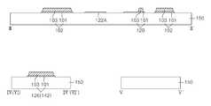
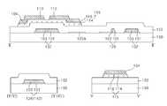
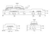
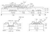
도 4는 본 발명의 실시 예에 따른 수평 전계 인가형 박막 트랜지스터 기판을 도시한 평면도이고, 도 5는 도 4에 도시된 박막 트랜지스터 기판을 Ⅲ-Ⅲ', Ⅳ-Ⅳ', Ⅴ-Ⅴ', Ⅵ-Ⅵ'선을 따라 절단하여 도시한 단면도이다.4 is a plan view showing a horizontal field applied thin film transistor substrate according to an embodiment of the present invention, Figure 5 is a thin film transistor substrate shown in Figure 4 III-III ', IV-IV', V-V ', It is sectional drawing cut along the VI-VI 'line.
도 4 및 도 5에 도시된 박막 트랜지스터 기판은 하부 기판(150) 위에 게이트 절연막(152)을 사이에 두고 교차하여 화소 영역을 정의하는 게이트 라인(102) 및 데이터 라인(104), 그 게이트 라인(102) 및 데이터 라인(104)과 화소 전극(118)에 접속된 박막 트랜지스터(TFT), 화소 영역에 수평 전계를 형성하도록 형성된 화소 전극(118) 및 공통 전극(122), 공통 전극(122)과 접속된 공통 라인(120)을 구비한다. 그리고, 박막 트랜지스터 기판은 공통 전극(122)과 화소 전극(118)의 중첩부 및 공통 라인(120)과 화소 전극(118)의 중첩부에 각각 형성된 제1 및 제2 스토리지 캐패시터(Cst1, Cst2), 게이트 라인(102)과 접속된 게이트 패드(124), 데이터 라인(104)과 접속된 데이터 패드(132), 공통 라인(120)과 접속된 공통 패드(140)를 더 구비한다.4 and 5 include a
게이트 라인(102)은 게이트 드라이버(미도시)로부터의 스캔 신호를, 데이터 라인(104)은 데이터 드라이버(미도시)로부터의 비디오 신호를 공급한다. 이러한 게이트 라인(102) 및 데이터 라인(104)은 게이트 절연막(152)을 사이에 두고 교차하여 각 화소 영역을 정의한다. 여기서, 게이트 라인(102)은 투명한 도전층으로 이루어진 제1 도전층(101), 불투명한 금속으로 이루어진 제2 도전층(103)이 적층된 이중 구조로 형성된다.
박막 트랜지스터(TFT)는 게이트 라인(102)의 스캔 신호에 응답하여 데이터 라인(104) 상의 비디오 신호가 화소 전극(118)에 충전되어 유지되게 한다. 이를 위하여, 박막 트랜지스터(TFT)는 게이트 라인(102)에 포함된 게이트 전극, 데이터 라인(104)과 접속된 소스 전극(110), 소스 전극(110)과 마주하며 화소 전극(118)과 접속된 드레인 전극(112), 게이트 절연막(152)을 사이에 두고 게이트 라인(102)과 중첩되어 소스 전극(110)과 드레인 전극(112) 사이에 채널을 형성하는 활성층(114), 소스 전극(110) 및 드레인 전극(112)과의 오믹 접촉을 위하여 채널부를 제외한 활성층(114) 위에 형성된 오믹 컨택층(116)을 구비한다.The thin film transistor TFT keeps the video signal on the
그리고, 활성층(114) 및 오믹 컨택층(116)을 포함하는 반도체 패턴(115)은 데이터 라인(104) 및 데이터 패드 하부 전극(134)과도 중첩되도록 형성된다.The
공통 라인(120) 및 공통 전극(122)은 액정 구동을 위한 기준 전압, 즉 공통 전압을 각 화소에 공급한다.The
이를 위하여, 공통 라인(120)은 표시 영역에서 게이트 라인(102)과 나란하게 형성된 내부 공통 라인(120A), 비표시 영역에서 내부 공통 라인(120A)과 공통 접속된 외부 공통 라인(120B)을 구비한다. 이러한 공통 라인(120)은 상기 게이트 라인(102)과 같이 제1 및 제2 도전층(101, 103)이 적층된 이중 구조로 형성된다.To this end, the
공통 전극(122)은 각 화소 영역에서 내부 공통 라인(120A)과 접속된다. 구체적으로, 공통 전극(122)은 내부 공통 라인(120A)의 제1 도전층(101)으로부터 화소 영역으로 신장된 핑거부(122B), 핑거부(122B)와 접속된 수평부(122A)를 구비한다. 이러한 공통 전극(122)은 공통 라인(120)의 제1 도전층(101)과 같은 투명 도전층으로 형성된다.The
화소 전극(118)은 박막 트랜지스터(TFT)의 드레인 전극(112)과 접속되며, 각 화소 영역에서 공통 전극(118)과 수평 전계를 형성하도록 형성된다. 구체적으로, 화소 전극(118)은 게이트 라인(102)과 나란하게 형성되어 제1 컨택홀(108)을 통해 노출된 드레인 전극(112)과 접속된 제1 수평부(118A), 내부 공통 라인(120A)과 중첩되게 형성된 제2 수평부(118C), 제1 및 제2 수평부(118A, 118C) 사이에 접속되어 공통 전극(122)의 핑거부(122B)와 나란하도록 형성된 핑커부(118B)를 구비한다. 이러한 화소 전극(118)에 박막 트랜지스터(TFT)를 통해 비디오 신호가 공급되면, 화소 전극(118)의 핑거부(118B)와 공통 라인(120)을 통해 공통 전압이 공급된 공통 전극(122)의 핑거부(122B) 사이에는 수평 전계가 형성된다. 이러한 수평 전계에 의해 박막 트랜지스터 기판과 칼라 필터 기판 사이에서 수평 방향으로 배열된 액정 분자들이 유전 이방성에 의해 회전하게 된다. 그리고, 액정 분자들의 회전 정도에 따라 화소 영역을 투과하는 광 투과율이 달라지게 됨으로써 계조를 구현하게 된다.The
스토리지 캐패시터는 화소 전극(118)의 제1 수평부(118A)가 보호막(154) 및 게이트 절연막(152)을 사이에 두고 공통 전극(122)의 수평부(122A)와 중첩되어 형성된 제1 스토리지 캐패시터(Cst1)와, 화소 전극(118)의 제2 수평부(118C)가 보호막(154) 및 게이트 절연막(152)을 사이에 두고 내부 공통 라인(120A)과 중첩되어 형성된 제2 스토리지 캐패시터(Cst2)를 구비한다. 여기서, 공통 라인(120)의 제1 도전층(101)에서 화소 전극(118)과 중첩되어질 일부분의 선폭을 상대적으로 크게 하여 화소 전극(118)과의 중첩 면적을 증가시킴으로써 개구율 감소 없이 제2 스토리지 캐패시터(Cst2)의 용량을 증가시킬 수 있게 된다. 나아가, 제1 및 제2 스토리지 캐패시터(Cst1, Cst2)는 화소 전극(118)과 공통 전극(122), 또는 공통 라인(120)을 공유하여 병렬 접속되므로 스토리지 캐패시터의 용량을 더욱 증가시킬 수 있게 된다. 여기서, 스토리지 캐패시터로 제1 및 제2 스토리지 캐패시터(Cst1, Cst2) 중 어느 하나만을 구비하는 것도 가능하다.The storage capacitor includes a first storage capacitor formed by overlapping the
이러한 이러한 스토리지 캐패시터는 화소 전극(118)에 충전된 화소 신호가 다음 화소 신호가 충전될 때까지 보다 안정적으로 유지되게 한다.This storage capacitor allows the pixel signal charged in the
게이트 라인(102)은 게이트 패드(124)를 통해 게이트 드라이버(미도시)와 접속된다. 게이트 패드(124)는 게이트 라인(102)으로부터 연장된 게이트 패드 하부 전극(126), 게이트 절연막(152) 및 보호막(154)을 관통하는 제2 컨택홀(128)을 통해 노출된 게이트 패드 하부 전극(126)과 접속된 게이트 패드 상부 전극(130)을 구 비한다. 여기서, 게이트 패드 하부 전극(126)은 게이트 라인(102)과 같이 제1 및 제2 도전층(101, 103)이 적층된 이중 구조를 갖는다.The
데이터 라인(104)은 데이터 패드(132)를 통해 데이터 드라이버(미도시)와 접속된다. 데이터 패드(132)는 데이터 라인(104)으로부터 그 아래의 반도체 패턴(115)과 함께 연장된 데이터 패드 하부 전극(134), 보호막(154)을 관통하는 제3 컨택홀(136)을 통해 노출된 데이터 패드 하부 전극(134)과 접속된 데이터 패드 상부 전극(138)을 구비한다.The
공통 라인(120)은 공통 패드(140)를 통해 공통 전압원(미도시)으로부터의 기준 전압을 공급받게 된다. 공통 패드(140)는 외부 공통 라인(120B)으로부터 연장된 공통 패드 하부 전극(142), 게이트 절연막(152) 및 보호막(154)을 관통하는 제4 컨택홀(144)을 통해 노출된 공통 패드 하부 전극(142)과 접속된 공통 패드 상부 전극(146)을 구비한다. 여기서, 공통 패드 하부 전극(142)은 공통 라인(120)과 같이 제1 및 제2 도전층(101, 103)이 적층된 이중 구조를 갖는다.The
이와 같이, 본 발명의 실시 예에 따른 수평 전계 인가형 박막 트랜지스터 기판에서는 공통 전극(122)이 투명 도전층인 제1 도전층(101)으로 형성되므로 그로 인한 개구율 저하를 방지할 수 있게 된다. 또한, 공통 라인(120)은 제1 및 제2 도전층(101, 103)이 적층된 이중 구조로 형성되어 라인 저항을 줄일 수 있게 된다. 그리고, 스토리지 캐패시터는 제1 및 제2 스토리지 캐패시터(Cst1, Cst2)가 병렬로 접속되어 구성되므로 개구율 감소 없이 용량을 증가시킬 수 있게 된다.As described above, in the horizontal field applied thin film transistor substrate according to the exemplary embodiment of the present invention, since the
이러한 장점을 갖는 본 발명에 따른 박막 트랜지스터 기판은 다음과 같이 4 마스크 공정으로 형성된다.The thin film transistor substrate according to the present invention having such an advantage is formed in a four mask process as follows.
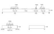
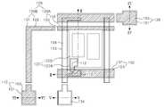
도 6a 및 도 6b는 본 발명의 실시 예에 따른 반투과형 박막 트랜지스터 기판 제조 방법 중 제1 마스크 공정을 설명하기 위한 평면도 및 단면도를, 도 7a 내지 도 7c는 제1 마스크 공정을 구체적으로 설명하기 위한 단면도들을 도시한 것이다.6A and 6B are plan and cross-sectional views illustrating a first mask process in a method of manufacturing a transflective thin film transistor substrate according to an exemplary embodiment of the present invention, and FIGS. 7A to 7C are diagrams for describing the first mask process in detail. Cross-sectional views are shown.
제1 마스크 공정으로 하부 기판(142) 상에 게이트 라인(102), 게이트 패드 하부 전극(126)을 포함하는 게이트 패턴과; 공통 라인(120), 공통 전극(122), 공통 패드 하부 전극(142)을 포함하는 공통 패턴이 형성된다. 여기서, 게이트 패턴과 공통 라인 및 패드(120, 142)는 제1 및 제2 도전층(101, 103)이 적층된 이중 구조로, 내부 공통 라인(120A)의 일부분 및 공통 전극(122)은 공통 라인(120)의 제1 도전층(101)으로부터 연장된 단일층 구조로 형성된다. 이렇게 이중 구조 및 단일층 구조를 갖는 게이트 및 공통 패턴은 하프 톤(Half Tone) 마스크 또는 회절 노광 마스크를 이용함으로써 하나의 마스크 공정으로 형성된다. 이하에서는 제1 마스크로 하프 톤 마스크를 이용한 경우를 예로 들어 설명하기로 한다.A gate pattern including a
구체적으로, 도 7a에 도시된 바와 같이 하부 기판(150) 상에 스퍼터링 방법 등의 증착 방법을 통해 제1 및 제2 도전층(101, 103)이 적층되고, 그 위에 포토레지스트(167)가 형성된다. 제1 도전층(101)으로는 ITO, TO, IZO 등과 같은 투명 도전 물질이, 제2 도전층(103)으로는 Mo, Ti, Cu, AlNd, Al, Cr, MoW계 등의 금속 물질이 이용된다. 그 다음, 하프 톤 마스크(160)를 이용한 포토리소그래피 공정으로 포토레지스트(167)를 노광 및 현상함으로써 도 7b에 도시된 바와 같이 단차를 갖는 포토레지스트 패턴(168)이 형성된다.Specifically, as shown in FIG. 7A, the first and second
하프 톤 마스크(260)는 도 7a와 같이 투명한 석영(SiO2; Quartz) 기판(166)과, 그 위에 형성된 부분 투과층(164) 및 차단층(162)을 구비한다. 부분 투과층(164)과 중첩된 차단층(162)은 게이트 패턴이 형성되어질 영역에 위치하여 자외선(UV)을 차단함으로써 현상 후 도 7b와 같이 제1 포토레지스트 패턴(168A)이 남게 한다. 차단층(162)과 비중첩된 부분 투과층(164)은 내부 공통 라인(120A)의 일부분 및 공통 전극(122)이 형성되어질 영역에 위치하여 자외선(UV)을 부분적으로 투과시킴으로써 현상 후 도 7b와 같이 제1 포토레지스트 패턴(168A) 보다 얇은 제2 포토레지스트 패턴(168B)이 남게 한다. 이를 위하여, 차단층(162)은 Cr, CrOx 등과 같은 금속으로, 부분 투과층(164)은 MoSix 등으로 형성된다.It includes a
이어서, 단차를 갖는 포토레지스트 패턴(168)을 이용한 식각 공정으로 제1 및 제2 도전층(101, 103)을 패터닝함으로써 도 7c에 도시된 바와 같이 이중층 구조의 게이트 패턴과 공통 라인(120) 및 공통 패드(142)와, 공통 전극(122)이 형성된다.Subsequently, the first and second
그 다음, 산소(O2) 플라즈마를 이용한 애싱 공정으로 포토레지스트 패턴(168)을 애싱함으로써 도 7d에 도시된 바와 같이 제1 포토레지스트 패턴(168A)은 두께가 얇아지게 되고, 제2 포토레지스 패턴(168B)은 제거된다. 그리고, 애싱된 제1 포토레지스트 패턴(168A)을 이용한 식각 공정으로 내부 공통 라인(120A)의 일부분 및 공통 전극(122) 위의 제2 도전층(103)이 제거된다. 이때, 애싱된 제1 포토레지스트 패턴(168A)을 따라 패터닝된 제2 도전층(103)의 양측부가 한번 더 식각 됨으로써 게이트 패턴과 공통 라인(120) 및 공통 패드(142)의 제1 및 제2 도전층(101, 103)은 계단 형태로 일정한 단차를 갖게 된다. 이에 따라, 제1 및 제2 도전층(101, 103)의 측면부가 높은 급경사를 갖게 될 경우 그 위에서 발생될 수 있는 소스/드레인 금속층의 단선 불량을 방지할 수 있게 된다.Then, by ashing the
그리고, 스트립 공정으로 게이트 패턴 위에 잔존하던 제1 포토레지스트 패턴(168A)이 도 7e에 도시된 바와 같이 제거됨으로써 이중 구조 및 단일층 구조를 갖는 게이트 및 공통 패턴이 완성된다.Then, the
도 8a 및 도 8b는 본 발명의 실시 예에 따른 박막 트랜지스터 기판 제조 방법 중 제2 마스크 공정을 설명하기 위한 평면도 및 단면도를 도시한 것이고, 도 9a 내지 도 9e는 제2 마스크 공정을 구체적으로 설명하기 위하 단면도들을 도시한 것이다.8A and 8B illustrate a plan view and a cross-sectional view for describing a second mask process in a method of manufacturing a thin film transistor substrate according to an exemplary embodiment of the present invention, and FIGS. 9A to 9E illustrate the second mask process in detail. Figures below are shown.
게이트 패턴이 형성된 하부 기판(150) 상에 게이트 절연막(152)이 형성되고, 그 위에 제2 마스크 공정으로 데이터 라인(104), 소스 전극(110), 드레인 전극(112), 데이터 패드 하부 전극(134)을 포함하는 소스/드레인 패턴과, 소스/드레인 패턴의 배면을 따라 중첩된 활성층(114) 및 오믹 컨택층(116)을 포함하는 반도체 패턴(115)이 형성된다. 이러한 반도체 패턴(115)과 소스/드레인 패턴은 회절 노광 마스크 또는 하프 톤 마스크를 이용한 하나의 마스크 공정으로 형성된다. 이하에서는 제2 마스크로 회절 노광 마스크를 이용한 경우를 설명하기로 한다.A
구체적으로, 도 9a와 같이 게이트 패턴이 형성된 하부 기판(150) 상에 게이트 절연막(152), 비정질 실리콘층(105), 불순물(n+ 또는 p+)이 도핑된 비정질 실리 콘층(107), 소스/드레인 금속층(109)이 순차적으로 형성된다. 예를 들면, 게이트 절연막(152), 비정질 실리콘층(105), 불순물이 도핑된 비정질 실리콘층(107)은 PECVD 방법으로, 소스/드레인 금속층(109)은 스퍼터링 방법으로 형성된다. 게이트 절연막(152)으로는 SiOx, SiNx 등과 같은 무기 절연 물질이, 소스/드레인 금속층(109)으로는 Cr, Mo, MoW, Al/Cr, Cu, Al(Nd), Al/Mo, Al(Nd)/Al, Al(Nd)/Cr, Mo/Al(Nd)/Mo, Cu/Mo, Ti/Al(Nd)/Ti 등이 이용된다. 그리고, 소스/드레인 금속층(109) 위에 포토레지스트(180)가 도포된 다음, 회절 노광 마스크(170)를 이용한 포토리소그래피 공정으로 포토레지스트(180)를 노광 및 현상함으로써 도 9b에 도시된 바와 같이 단차를 갖는 포토레지스트 패턴(182)이 형성된다.In detail, as illustrated in FIG. 9A, the
회절 노광 마스크(170)는 도 9a와 같이 투명한 석영 기판(172)과, 그 위에 Cr 등과 같은 금속층으로 형성된 차단층(174) 및 회절 노광용 슬릿(176)을 구비한다. 차단층(174)은 반도체 패턴 및 소스/드레인 패턴이 형성되어질 영역에 위치하여 자외선을 차단함으로써 현상 후 도 9b와 같이 제1 포토레지스트 패턴(182A)이 남게 한다. 회절 노광용 슬릿(176)은 박막 트랜지스터의 채널이 형성될 영역에 위치하여 자외선을 회절시킴으로써 현상 후 도 9b와 같이 제1 포토레지스트 패턴(182A) 보다 얇은 제2 포토레지스트 패턴(182B)이 남게 한다.The
이어서, 단차를 갖는 포토레지스트 패턴(182)을 이용한 식각 공정으로 소스/드레인 금속층(109)이 패터닝됨으로써 도 9c에 도시된 바와 같이 소스/드레인 패턴과, 그 아래의 반도체 패턴(115)이 형성된다. 이 경우, 소스/드레인 패턴 중 소스 전극(110)과 드레인 전극(112)은 일체화된 구조를 갖는다.Subsequently, the source /
그 다음, 산소(O2) 플라즈마를 이용한 애싱 공정으로 포토레지스트 패턴(182)을 애싱함으로써 도 9d에 도시된 바와 같이 제1 포토레지스트 패턴(182A)은 얇아지게 되고, 제2 포토레지스트 패턴(182B)은 제거된다. 그리고, 애싱된 제1 포토레지스트 패턴(182A)을 이용한 식각 공정으로 제2 포토레지스트 패턴(182B)의 제거로 노출된 소스/드레인 패턴과, 그 아래의 오믹 컨택층(116)이 제거됨으로써 소스 전극(110)과 드레인 전극(112)은 분리되고 활성층(114)이 노출된다. 이에 따라, 소스 전극(110)과 드레인 전극(112) 사이에는 활성층(114)으로 이루어진 채널이 형성된다. 이때, 애싱된 제1 포토레지스트 패턴(182A)을 따라 소스/드레인 패턴의 양측부가 한번 더 식각됨으로써 소스/드레인 패턴과 반도체 패턴(115)은 계단 형태로 일정한 단차를 갖게 된다.Then, by ashing the
그리고, 스트립 공정으로 소스/드레인 패턴 위에 잔존하던 제1 포토레지스트 패턴(182A)이 도 9e와 같이 제거됨으로써 반도체 패턴(115) 및 소스/드레인 패턴이 완성된다.The
도 10a 및 도 10b는 본 발명의 실시 예에 따른 박막 트랜지스터 기판 제조 방법 중 제3 마스크 공정을 설명하기 위한 평면도 및 단면도이다.10A and 10B are a plan view and a cross-sectional view for describing a third mask process in the method of manufacturing a thin film transistor substrate according to the exemplary embodiment of the present invention.
제3 마스크 공정으로 소스/드레인 패턴이 형성된 게이트 절연막(152) 상에 제1 내지 제4 컨택홀(108, 128, 136, 144)을 갖는 보호막(154)이 형성된다.The
구체적으로, 소스/드레인 패턴이 형성된 게이트 절연막(152) 상에 PECVD, 스핀 코팅(Spin Coating), 스핀리스 코팅(Spinless Coating) 등의 방법으로 보호막 (154)이 형성된다. 보호막(154)으로는 게이트 절연막(152)과 같은 무기 절연 물질, 또는 유기 절연 물질이 이용된다. 그리고, 보호막(154) 위에 제3 마스크를 이용한 포토리소그래피 공정 및 식각 공정으로 보호막(154) 및 게이트 절연막(152)이 패터닝됨으로써 제1 내지 제4 컨택홀(108, 128, 136, 144)이 형성된다. 여기서, 제1 및 제3 컨택홀(108, 136) 각각은 보호막(154)을 관통하여 드레인 전극(112)과 데이터 패드 하부 전극(134) 각각을, 제2 및 제4 컨택홀(128, 144) 각각은 보호막(154) 및 게이트 절연막(152)을 관통하여 게이트 패드 하부 전극(126) 및 공통 패드 하부 전극(142) 각각을 노출시킨다.Specifically, the
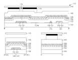
도 11a 및 도 11b는 본 발명의 실시 예에 따른 박막 트랜지스터 기판 제조 방법 중 제4 마스크 공정을 설명하기 위한 평면도 및 단면도이다.11A and 11B are plan and cross-sectional views illustrating a fourth mask process in the method of manufacturing a thin film transistor substrate according to an exemplary embodiment of the present invention.
제4 마스크 공정으로 보호막(154) 상에 화소 전극(118), 게이트 패드 상부 전극(130), 데이터 패드 상부 전극(138), 공통 패드 상부 전극(146)을 포함하는 투명 도전 패턴이 형성된다.In the fourth mask process, a transparent conductive pattern including the
구체적으로, 보호막(154) 상에 투명 도전층이 스퍼터링 등과 같은 증착 방법으로 형성된다. 투명 도전층으로는 상기 게이트 및 공통 패턴의 제1 도전층(101)과 같이 ITO, TO, IZO 등이 이용된다. 또한, 투명 도전층은 Ti, W 등과 같이 내식성이 강하고 강도가 높은 불투명한 금속으로도 대체될 수 있다. 그 다음, 제4 마스크를 이용한 포토리소그래피 공정 및 식각 공정으로 투명 도전층이 패터닝됨으로써 화소 전극(118), 게이트 패드 상부 전극(130), 데이터 패드 상부 전극(138), 공통 패드 상부 전극(146)을 포함하는 투명 도전 패턴이 형성된다. 이에 따라, 화소 전극(118), 게이트 패드 상부 전극(130), 데이터 패드 상부 전극(138), 공통 패드 상부 전극(146) 각각은 제1 내지 제4 컨택홀(108, 128, 136, 144) 각각을 통해 노출된 드레인 전극(112), 게이트 패드 하부 전극(126), 데이터 패드 하부 전극(134), 공통 패드 하부 전극(142) 각각과 접속된다. 예를 들면, 화소 전극(118), 게이트 패드 상부 전극(130), 데이터 패드 상부 전극(138), 공통 패드 상부 전극(146) 각각은 드레인 전극(112), 게이트 패드 하부 전극(126), 데이터 패드 하부 전극(134), 공통 패드 하부 전극(142) 각각의 표면과 접촉하게 된다.Specifically, the transparent conductive layer is formed on the
한편, 게이트 패턴 및 공통 패턴의 제2 도전층(103)과, 소스/드레인 패턴으로 Mo 등과 같이 건식 식각이 용이한 금속을 이용되는 경우 도 12와 같이 화소 전극(118), 게이트 패드 상부 전극(130), 데이터 패드 상부 전극(138), 공통 패드 상부 전극(146) 각각은 드레인 전극(112), 게이트 패드 하부 전극(126), 데이터 패드 하부 전극(134), 공통 패드 하부 전극(142) 각각과 측면 접촉하게 된다. 이는 제3 마스크 공정으로 보호막(154) 및 게이트 절연막(152)을 패터닝하는 경우 제2 및 제4 컨택홀(128, 144)이 게이트 패드 하부 전극(126) 및 공통 패드 하부 전극(142)의 제2 도전층(130)까지, 제1 및 제3 컨택홀(108, 136)이 드레인 전극(108) 및 데이터 패드 하부 전극(134)을 관통하기 때문이다. 특히, 제1 및 제3 컨택홀(108, 136)은 드레인 전극(108) 및 데이터 패드 하부 전극(134) 아래의 반도체 패턴(115)까지 관통하거나, 나아가 게이트 절연막(152)의 일부분까지 연장되기도 한다.On the other hand, when the second
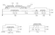
도 13은 본 발명의 다른 실시 예에 따른 수평 전계 인가형 박막 트랜지스터 기판을 도시한 평면도이고, 도 14는 도 13에 도시된 박막 트랜지스터 기판을 Ⅲ- Ⅲ', Ⅳ-Ⅳ', Ⅴ-Ⅴ', Ⅵ-Ⅵ', Ⅶ-Ⅶ'선을 따라 절단하여 도시한 단면도이다.FIG. 13 is a plan view illustrating a horizontal field applied thin film transistor substrate according to another exemplary embodiment of the present invention, and FIG. 14 illustrates III-III ', IV-IV', and V-V 'of the thin film transistor substrate shown in FIG. Sectional drawing cut along the lines VI-VI 'and VIII-VIII.
도 13 및 도 14에 도시된 박막 트랜지스터 기판은 도 4 및 도 5에 도시된 박막 트랜지스터 기판과 대비하여, 공통 전극(222)이 공통 라인(120)과 같이 제1 및 제2 도전층(101, 103)이 적층된 이중 구조로 형성된 것을 제외하고는 동일한 구성 요소들을 구비한다. 따라서, 중복되는 구성 요소들에 대한 설명은 생략하기로 한다.13 and 14, the
공통 전극(222)은 내부 공통 라인(120A)과 접속되며 투명한 제1 도전층(101)과 불투명한 제2 도전층(103)이 적층된 이중 구조를 갖는 핑거부(222B)와, 핑거부(222B)와 접속되며 제1 도전층(101)으로만 이루어진 단일층 구조를 갖는 수평부(222A)를 구비한다. 여기서, 핑거부(222B)의 제2 도전층(103)은 제1 도전층(101)으로 인한 빛샘 차단층 역할을 하게 된다. 이때, 핑거부(222B)의 제2 도전층(103)은 개구율에 기여하는 제1 도전층(101)의 양측부를 간섭하지 않도록 제1 도전층(101) 보다 작은 선폭을 갖게 된다. 예를 들면, 핑거부(222B)의 에지로부터 안쪽으로 약 1㎛ 정도까지 해당되는 제1 도전층(101)의 양측부는 개구율에 기여하므로, 이러한 제1 도전층(101)의 양측부를 제외한 나머지 부분과 중첩되도록 제2 도전층(103)을 형성하게 된다. 이에 따라, 공통 전극(222)의 핑거부(222B)는 제1 도전층(101)에 의해 개구율을 향상시키면서, 제2 도전층(103)에 의해 빛샘을 방지하여 컨트라스트(Contrast)를 향상시킬 수 있게 된다.The
이와 같이, 이중 구조를 갖는 공통 전극(222)의 핑거부(222B)와 단일층 구조를 갖는 수평부(222A)는 도 6a 내지 도 7e에서 전술한 바와 같이 하프 톤 마스크 또는 회절 노광 마스크를 이용한 제1 마스크 공정으로 형성된다. 이 경우, 핑거부(222B)에서 제1 및 제2 도전층(101, 103)의 중첩부는 하프 톤 마스크(또는 회절 노광 마스크)의 차단부에 대응하여 형성되고, 제2 도전층(103)과 비중첩된 제1 도전층(101)의 양측부는 부분 투과부(또는 회절 노광부)를에 대응하여 형성된다.
As described above, the
상술한 바와 같이, 본 발명에 따른 수평 전계 인가형 박막 트랜지스터 기판 및 그 제조 방법은 투명한 제1 도전층으로 이루어진 공통 전극을 그 제1 도전층을 포함하는 이중 구조의 게이트 패턴 및 다른 공통 패턴과 동일한 마스크 공정으로 형성하게 된다. 이에 따라, 4마스크 공정으로 공정을 단순화하면서도 개구율을 향상시킬 수 있게 된다. 또한, 스토리지 캐패시터는 병렬 접속된 제1 및 제2 스토리지 캐패시터를 구비하므로 개구율 감소 없이도 용량을 증가시킬 수 있게 된다.As described above, the horizontal field-applied thin film transistor substrate according to the present invention and a manufacturing method thereof have the same common electrode formed of the transparent first conductive layer as the gate pattern of the dual structure including the first conductive layer and other common patterns. It is formed by a mask process. Accordingly, the aperture ratio can be improved while simplifying the process with a four mask process. In addition, since the storage capacitor includes the first and second storage capacitors connected in parallel, the capacity can be increased without reducing the aperture ratio.
나아가, 본 발명에 따른 수평 전계 인가형 박막 트랜지스터 기판 및 그 제조 방법은 공통 전극의 핑거부는 투명한 제1 도전층 보다 작은 선폭으로 중첩된 불투명한 제2 도전층을 추가로 구비함으로써 제2 도전층과 비중첩된 제1 도전층의 양측부에 개구율을 향상시킴과 아울러 제2 도전층에 의해 빛샘을 방지하여 컨트라스트를 향상시킬 수 있게 된다.Furthermore, the horizontal field-applied thin film transistor substrate and the method of manufacturing the same according to the present invention further include an opaque second conductive layer superimposed with a smaller line width than the transparent first conductive layer, thereby providing a second conductive layer and a second conductive layer. It is possible to improve the aperture ratio on both sides of the non-overlapping first conductive layer and to prevent light leakage by the second conductive layer to improve contrast.
이상 설명한 내용을 통해 당업자라면 본 발명의 기술사상을 일탈하지 아니하는 범위에서 다양한 변경 및 수정이 가능함을 알 수 있을 것이다. 따라서, 본 발명의 기술적 범위는 명세서의 상세한 설명에 기재된 내용으로 한정되는 것이 아니 라 특허 청구의 범위에 의해 정하여져야만 할 것이다.Those skilled in the art will appreciate that various changes and modifications can be made without departing from the technical spirit of the present invention. Therefore, the technical scope of the present invention should not be limited to the contents described in the detailed description of the specification but should be defined by the claims.
Claims (29)
Translated fromKoreanPriority Applications (3)
| Application Number | Priority Date | Filing Date | Title |
|---|---|---|---|
| KR1020040047574AKR101002347B1 (en) | 2004-06-24 | 2004-06-24 | Horizontal field applied thin film transistor substrate and manufacturing method thereof |
| US11/236,831US7316944B2 (en) | 2004-06-24 | 2005-09-28 | Fabricating method of a liquid crystal display device |
| US11/984,990US7858984B2 (en) | 2004-06-24 | 2007-11-26 | Liquid crystal display device having a double layered structure and a single layered structure on the same layer |
Applications Claiming Priority (1)
| Application Number | Priority Date | Filing Date | Title |
|---|---|---|---|
| KR1020040047574AKR101002347B1 (en) | 2004-06-24 | 2004-06-24 | Horizontal field applied thin film transistor substrate and manufacturing method thereof |
Publications (2)
| Publication Number | Publication Date |
|---|---|
| KR20050122465A KR20050122465A (en) | 2005-12-29 |
| KR101002347B1true KR101002347B1 (en) | 2010-12-21 |
Family
ID=35656198
Family Applications (1)
| Application Number | Title | Priority Date | Filing Date |
|---|---|---|---|
| KR1020040047574AExpired - LifetimeKR101002347B1 (en) | 2004-06-24 | 2004-06-24 | Horizontal field applied thin film transistor substrate and manufacturing method thereof |
Country Status (2)
| Country | Link |
|---|---|
| US (2) | US7316944B2 (en) |
| KR (1) | KR101002347B1 (en) |
Families Citing this family (23)
| Publication number | Priority date | Publication date | Assignee | Title |
|---|---|---|---|---|
| CN1139837C (en)* | 1998-10-01 | 2004-02-25 | 三星电子株式会社 | Film transistor array substrate for liquid crystal display and manufacture thereof |
| KR101066489B1 (en)* | 2004-11-12 | 2011-09-21 | 엘지디스플레이 주식회사 | Poly-type thin film transistor substrate and manufacturing method thereof |
| KR101192746B1 (en)* | 2004-11-12 | 2012-10-18 | 엘지디스플레이 주식회사 | Method of Fabricating Thin Film Transistor Substrate of Poly-type |
| KR101127822B1 (en)* | 2004-12-24 | 2012-03-26 | 엘지디스플레이 주식회사 | Thin film transistor substrate of horizontal electric field and fabricating method thereof |
| KR101234214B1 (en)* | 2006-03-06 | 2013-02-18 | 엘지디스플레이 주식회사 | Liquid crystal display device and method of fabricating the same |
| KR101421166B1 (en)* | 2007-03-02 | 2014-07-18 | 엘지디스플레이 주식회사 | Method of fabricating liquid crystal display device |
| TWI334647B (en)* | 2007-03-03 | 2010-12-11 | Au Optronics Corp | Method for manufacturing pixel structure |
| KR101374105B1 (en)* | 2007-08-09 | 2014-03-14 | 엘지디스플레이 주식회사 | Thin Film Transistor Substrate And Manufacturing Method Thereof |
| US9041202B2 (en) | 2008-05-16 | 2015-05-26 | Semiconductor Energy Laboratory Co., Ltd. | Semiconductor device and manufacturing method of the same |
| JP2010056541A (en) | 2008-07-31 | 2010-03-11 | Semiconductor Energy Lab Co Ltd | Semiconductor device and manufacturing method thereof |
| TWI469354B (en) | 2008-07-31 | 2015-01-11 | Semiconductor Energy Lab | Semiconductor device and method of manufacturing same |
| JP5771365B2 (en)* | 2009-11-23 | 2015-08-26 | 三星ディスプレイ株式會社Samsung Display Co.,Ltd. | Medium and small liquid crystal display |
| CN102884633B (en)* | 2010-05-13 | 2013-11-13 | 夏普株式会社 | Circuit board and display device |
| US8558960B2 (en) | 2010-09-13 | 2013-10-15 | Semiconductor Energy Laboratory Co., Ltd. | Liquid crystal display device and method for manufacturing the same |
| KR101875044B1 (en)* | 2011-07-19 | 2018-07-06 | 엘지디스플레이 주식회사 | Array substrate of gate in panel type liquid crystal display device |
| KR101938761B1 (en)* | 2012-05-23 | 2019-01-16 | 삼성디스플레이 주식회사 | Thin-film transistor array substrate, organic light emitting display device comprising the same and manufacturing method of the same |
| EP3404375A1 (en)* | 2013-05-17 | 2018-11-21 | VEGA Grieshaber KG | Measuring device control for determining a topology of a surface of a bulk material |
| CN104517989B (en)* | 2013-09-30 | 2017-12-29 | 昆山国显光电有限公司 | A kind of organic light-emitting display device and preparation method thereof |
| KR102118461B1 (en)* | 2013-11-25 | 2020-06-09 | 엘지디스플레이 주식회사 | Array substrate including oxide thin film transitor and method of fabricating the same |
| US9965122B2 (en)* | 2015-12-28 | 2018-05-08 | Lg Display Co., Ltd. | Display device with light shield |
| US9910523B2 (en)* | 2015-12-28 | 2018-03-06 | Lg Display Co., Ltd. | Display device with connection interface for common signal lines placed under planarization layer |
| CN106024909B (en)* | 2016-07-27 | 2021-01-26 | 京东方科技集团股份有限公司 | Thin film transistor, preparation method thereof, array substrate and display device |
| CN107204375B (en)* | 2017-05-19 | 2019-11-26 | 深圳市华星光电技术有限公司 | Thin film transistor and its manufacturing method |
Citations (2)
| Publication number | Priority date | Publication date | Assignee | Title |
|---|---|---|---|---|
| US20020097349A1 (en) | 1999-11-05 | 2002-07-25 | Woon-Yong Park | Thin film transistor array panel for liquid crystal display |
| US20030193639A1 (en) | 2002-04-15 | 2003-10-16 | Advanced Display Inc. | Liquid crystal display device and method of manufacturing the same |
Family Cites Families (16)
| Publication number | Priority date | Publication date | Assignee | Title |
|---|---|---|---|---|
| US5162933A (en) | 1990-05-16 | 1992-11-10 | Nippon Telegraph And Telephone Corporation | Active matrix structure for liquid crystal display elements wherein each of the gate/data lines includes at least a molybdenum-base alloy layer containing 0.5 to 10 wt. % of chromium |
| KR940004322B1 (en) | 1991-09-05 | 1994-05-19 | 삼성전자 주식회사 | Liquid crystal display devices |
| US5317433A (en) | 1991-12-02 | 1994-05-31 | Canon Kabushiki Kaisha | Image display device with a transistor on one side of insulating layer and liquid crystal on the other side |
| DE4339721C1 (en) | 1993-11-22 | 1995-02-02 | Lueder Ernst | Method for producing a matrix of thin-film transistors |
| TW321731B (en) | 1994-07-27 | 1997-12-01 | Hitachi Ltd | |
| JP3866783B2 (en) | 1995-07-25 | 2007-01-10 | 株式会社 日立ディスプレイズ | Liquid crystal display |
| KR0156202B1 (en) | 1995-08-22 | 1998-11-16 | 구자홍 | LCD and its manufacturing method |
| JPH09113931A (en) | 1995-10-16 | 1997-05-02 | Sharp Corp | Liquid crystal display |
| JP3625598B2 (en) | 1995-12-30 | 2005-03-02 | 三星電子株式会社 | Manufacturing method of liquid crystal display device |
| WO1998027454A1 (en) | 1996-12-18 | 1998-06-25 | Hitachi, Ltd. | Transverse electric field system liquid crystal display device suitable for improving aperture ratio |
| KR100590744B1 (en)* | 1998-10-30 | 2006-10-13 | 삼성전자주식회사 | A color filter substrate, a manufacturing method thereof, and a liquid crystal display including the color filter substrate. |
| JP2002139737A (en) | 2000-07-31 | 2002-05-17 | Matsushita Electric Ind Co Ltd | Liquid crystal display device and manufacturing method thereof |
| KR100748442B1 (en)* | 2001-02-26 | 2007-08-10 | 엘지.필립스 엘시디 주식회사 | Array board for horizontal electric field drive type liquid crystal display device and manufacturing method thereof |
| US6940573B2 (en)* | 2001-11-22 | 2005-09-06 | Samsung Electronics, Co., Ltd. | Liquid crystal display and thin film transistor array panel |
| KR20050091291A (en) | 2004-03-11 | 2005-09-15 | 엘지.필립스 엘시디 주식회사 | In plane switching mode liquid crystal display device and method of fabricating thereof |
| KR101085136B1 (en) | 2004-12-04 | 2011-11-18 | 엘지디스플레이 주식회사 | Horizontal field thin film transistor substrate and its manufacturing method |
- 2004
- 2004-06-24KRKR1020040047574Apatent/KR101002347B1/ennot_activeExpired - Lifetime
- 2005
- 2005-09-28USUS11/236,831patent/US7316944B2/ennot_activeExpired - Lifetime
- 2007
- 2007-11-26USUS11/984,990patent/US7858984B2/enactiveActive
Patent Citations (2)
| Publication number | Priority date | Publication date | Assignee | Title |
|---|---|---|---|---|
| US20020097349A1 (en) | 1999-11-05 | 2002-07-25 | Woon-Yong Park | Thin film transistor array panel for liquid crystal display |
| US20030193639A1 (en) | 2002-04-15 | 2003-10-16 | Advanced Display Inc. | Liquid crystal display device and method of manufacturing the same |
Also Published As
| Publication number | Publication date |
|---|---|
| US7858984B2 (en) | 2010-12-28 |
| US7316944B2 (en) | 2008-01-08 |
| US20080073651A1 (en) | 2008-03-27 |
| US20060017054A1 (en) | 2006-01-26 |
| KR20050122465A (en) | 2005-12-29 |
Similar Documents
| Publication | Publication Date | Title |
|---|---|---|
| KR101085136B1 (en) | Horizontal field thin film transistor substrate and its manufacturing method | |
| KR101002347B1 (en) | Horizontal field applied thin film transistor substrate and manufacturing method thereof | |
| KR101085132B1 (en) | Horizontal field thin film transistor substrate and its manufacturing method | |
| KR101201017B1 (en) | Liquid crystal display and fabricating method thereof | |
| KR100499371B1 (en) | Thin film transistor array substrate and method of manufacturing the same | |
| KR101225440B1 (en) | Liquid crystal display and fabricating method thereof | |
| KR101086478B1 (en) | Thin film transistor substrate for display element and manufacturing method thereof | |
| KR101086477B1 (en) | Method for manufacturing thin film transistor substrate for display element | |
| KR101121620B1 (en) | Thin Film Transistor Substrate for Display Device And Method For Fabricating The Same | |
| KR100560402B1 (en) | Horizontal field applied thin film transistor substrate and manufacturing method thereof | |
| KR101139522B1 (en) | Thin Film Transistor Substrate of Transflective Type And Method for Fabricating The Same | |
| KR100560399B1 (en) | Horizontal field applied thin film transistor substrate and manufacturing method thereof | |
| KR100566816B1 (en) | Horizontal field applied thin film transistor substrate and manufacturing method thereof | |
| KR101107245B1 (en) | Horizontal field thin film transistor substrate and its manufacturing method | |
| KR20060136287A (en) | Liquid crystal display and fabricating method thereof | |
| KR100560405B1 (en) | Horizontal field applied thin film transistor substrate and manufacturing method thereof | |
| KR101107269B1 (en) | Horizontal field thin film transistor substrate and its manufacturing method, liquid crystal panel using the same, and its manufacturing method | |
| KR101085142B1 (en) | Horizontal field thin film transistor substrate and its manufacturing method | |
| KR101107265B1 (en) | Horizontal field thin film transistor substrate and its manufacturing method, liquid crystal panel using the same, and its manufacturing method | |
| KR100560403B1 (en) | Horizontal field applied thin film transistor substrate and manufacturing method thereof | |
| JP4537929B2 (en) | Liquid crystal display device and method of manufacturing liquid crystal display device | |
| KR101066492B1 (en) | Thin film transistor substrate and its manufacturing method | |
| KR101127822B1 (en) | Thin film transistor substrate of horizontal electric field and fabricating method thereof | |
| KR101096718B1 (en) | Fabricating method of thin film transistor substrate of horizontal electric field | |
| KR101341774B1 (en) | Liquid Crystal Display and Method For Manufacturing of The Same |
Legal Events
| Date | Code | Title | Description |
|---|---|---|---|
| PA0109 | Patent application | Patent event code:PA01091R01D Comment text:Patent Application Patent event date:20040624 | |
| PG1501 | Laying open of application | ||
| A201 | Request for examination | ||
| PA0201 | Request for examination | Patent event code:PA02012R01D Patent event date:20090427 Comment text:Request for Examination of Application Patent event code:PA02011R01I Patent event date:20040624 Comment text:Patent Application | |
| E701 | Decision to grant or registration of patent right | ||
| PE0701 | Decision of registration | Patent event code:PE07011S01D Comment text:Decision to Grant Registration Patent event date:20101125 | |
| GRNT | Written decision to grant | ||
| PR0701 | Registration of establishment | Comment text:Registration of Establishment Patent event date:20101213 Patent event code:PR07011E01D | |
| PR1002 | Payment of registration fee | Payment date:20101214 End annual number:3 Start annual number:1 | |
| PG1601 | Publication of registration | ||
| FPAY | Annual fee payment | Payment date:20130930 Year of fee payment:4 | |
| PR1001 | Payment of annual fee | Payment date:20130930 Start annual number:4 End annual number:4 | |
| FPAY | Annual fee payment | Payment date:20141124 Year of fee payment:5 | |
| PR1001 | Payment of annual fee | Payment date:20141124 Start annual number:5 End annual number:5 | |
| FPAY | Annual fee payment | Payment date:20161118 Year of fee payment:7 | |
| PR1001 | Payment of annual fee | Payment date:20161118 Start annual number:7 End annual number:7 | |
| FPAY | Annual fee payment | Payment date:20171116 Year of fee payment:8 | |
| PR1001 | Payment of annual fee | Payment date:20171116 Start annual number:8 End annual number:8 | |
| FPAY | Annual fee payment | Payment date:20181114 Year of fee payment:9 | |
| PR1001 | Payment of annual fee | Payment date:20181114 Start annual number:9 End annual number:9 | |
| PR1001 | Payment of annual fee | Payment date:20201119 Start annual number:11 End annual number:11 | |
| PR1001 | Payment of annual fee | Payment date:20211116 Start annual number:12 End annual number:12 | |
| PR1001 | Payment of annual fee | Payment date:20221115 Start annual number:13 End annual number:13 | |
| PR1001 | Payment of annual fee | Payment date:20231115 Start annual number:14 End annual number:14 | |
| PC1801 | Expiration of term | Termination date:20241224 Termination category:Expiration of duration |