KR101002260B1 - Mixed Plasma Reactor - Google Patents
Mixed Plasma ReactorDownload PDFInfo
- Publication number
- KR101002260B1 KR101002260B1KR1020080042581AKR20080042581AKR101002260B1KR 101002260 B1KR101002260 B1KR 101002260B1KR 1020080042581 AKR1020080042581 AKR 1020080042581AKR 20080042581 AKR20080042581 AKR 20080042581AKR 101002260 B1KR101002260 B1KR 101002260B1
- Authority
- KR
- South Korea
- Prior art keywords
- plasma
- antenna
- reactor
- antenna electrodes
- radio frequency
- Prior art date
- Legal status (The legal status is an assumption and is not a legal conclusion. Google has not performed a legal analysis and makes no representation as to the accuracy of the status listed.)
- Active
Links
- 239000000758substrateSubstances0.000claimsabstractdescription33
- 238000009826distributionMethods0.000claimsdescription18
- 238000000034methodMethods0.000claimsdescription16
- 238000002347injectionMethods0.000claimsdescription12
- 239000007924injectionSubstances0.000claimsdescription12
- 238000001816coolingMethods0.000claimsdescription6
- 239000000203mixtureSubstances0.000claimsdescription2
- 238000009616inductively coupled plasmaMethods0.000abstractdescription11
- 239000007789gasSubstances0.000description37
- 238000004519manufacturing processMethods0.000description8
- 238000012545processingMethods0.000description8
- 150000002500ionsChemical class0.000description6
- 239000004065semiconductorSubstances0.000description6
- 230000008878couplingEffects0.000description5
- 238000010168coupling processMethods0.000description5
- 238000005859coupling reactionMethods0.000description5
- 230000001965increasing effectEffects0.000description4
- 230000008569processEffects0.000description4
- 229910052782aluminiumInorganic materials0.000description3
- XAGFODPZIPBFFR-UHFFFAOYSA-NaluminiumChemical compound[Al]XAGFODPZIPBFFR-UHFFFAOYSA-N0.000description3
- 238000010586diagramMethods0.000description3
- 238000010849ion bombardmentMethods0.000description3
- 230000004048modificationEffects0.000description3
- 238000012986modificationMethods0.000description3
- 238000009832plasma treatmentMethods0.000description3
- PXHVJJICTQNCMI-UHFFFAOYSA-NNickelChemical compound[Ni]PXHVJJICTQNCMI-UHFFFAOYSA-N0.000description2
- 230000003247decreasing effectEffects0.000description2
- 238000005516engineering processMethods0.000description2
- 239000011521glassSubstances0.000description2
- 239000000463materialSubstances0.000description2
- 229910052751metalInorganic materials0.000description2
- 239000002184metalSubstances0.000description2
- 239000007769metal materialSubstances0.000description2
- 239000010453quartzSubstances0.000description2
- VYPSYNLAJGMNEJ-UHFFFAOYSA-Nsilicon dioxideInorganic materialsO=[Si]=OVYPSYNLAJGMNEJ-UHFFFAOYSA-N0.000description2
- RYGMFSIKBFXOCR-UHFFFAOYSA-NCopperChemical compound[Cu]RYGMFSIKBFXOCR-UHFFFAOYSA-N0.000description1
- XUIMIQQOPSSXEZ-UHFFFAOYSA-NSiliconChemical compound[Si]XUIMIQQOPSSXEZ-UHFFFAOYSA-N0.000description1
- 238000004380ashingMethods0.000description1
- 230000004888barrier functionEffects0.000description1
- 230000008901benefitEffects0.000description1
- 230000005540biological transmissionEffects0.000description1
- 239000000919ceramicSubstances0.000description1
- 238000004140cleaningMethods0.000description1
- 238000010276constructionMethods0.000description1
- 229910052802copperInorganic materials0.000description1
- 239000010949copperSubstances0.000description1
- 238000000151depositionMethods0.000description1
- 230000008021depositionEffects0.000description1
- 238000011161developmentMethods0.000description1
- 230000009977dual effectEffects0.000description1
- 230000000694effectsEffects0.000description1
- 239000012777electrically insulating materialSubstances0.000description1
- 238000005530etchingMethods0.000description1
- 230000005284excitationEffects0.000description1
- 230000001939inductive effectEffects0.000description1
- 238000009434installationMethods0.000description1
- 238000009413insulationMethods0.000description1
- 239000004973liquid crystal related substanceSubstances0.000description1
- 229910052759nickelInorganic materials0.000description1
- 229910052755nonmetalInorganic materials0.000description1
- 238000013021overheatingMethods0.000description1
- 239000003870refractory metalSubstances0.000description1
- 229910052710siliconInorganic materials0.000description1
- 239000010703siliconSubstances0.000description1
- 229910001220stainless steelInorganic materials0.000description1
- 239000010935stainless steelSubstances0.000description1
- 239000013077target materialSubstances0.000description1
- 239000010409thin filmSubstances0.000description1
Images


Classifications
- H—ELECTRICITY
- H01—ELECTRIC ELEMENTS
- H01J—ELECTRIC DISCHARGE TUBES OR DISCHARGE LAMPS
- H01J37/00—Discharge tubes with provision for introducing objects or material to be exposed to the discharge, e.g. for the purpose of examination or processing thereof
- H01J37/32—Gas-filled discharge tubes
- H01J37/32009—Arrangements for generation of plasma specially adapted for examination or treatment of objects, e.g. plasma sources
- H01J37/32082—Radio frequency generated discharge
- H01J37/32091—Radio frequency generated discharge the radio frequency energy being capacitively coupled to the plasma
- H—ELECTRICITY
- H01—ELECTRIC ELEMENTS
- H01J—ELECTRIC DISCHARGE TUBES OR DISCHARGE LAMPS
- H01J37/00—Discharge tubes with provision for introducing objects or material to be exposed to the discharge, e.g. for the purpose of examination or processing thereof
- H01J37/32—Gas-filled discharge tubes
- H01J37/32009—Arrangements for generation of plasma specially adapted for examination or treatment of objects, e.g. plasma sources
- H01J37/32082—Radio frequency generated discharge
- H01J37/321—Radio frequency generated discharge the radio frequency energy being inductively coupled to the plasma
- H01J37/3211—Antennas, e.g. particular shapes of coils
- H—ELECTRICITY
- H01—ELECTRIC ELEMENTS
- H01J—ELECTRIC DISCHARGE TUBES OR DISCHARGE LAMPS
- H01J37/00—Discharge tubes with provision for introducing objects or material to be exposed to the discharge, e.g. for the purpose of examination or processing thereof
- H01J37/32—Gas-filled discharge tubes
- H01J37/32009—Arrangements for generation of plasma specially adapted for examination or treatment of objects, e.g. plasma sources
- H01J37/32082—Radio frequency generated discharge
- H01J37/32174—Circuits specially adapted for controlling the RF discharge
- H01J37/32183—Matching circuits
- H—ELECTRICITY
- H01—ELECTRIC ELEMENTS
- H01J—ELECTRIC DISCHARGE TUBES OR DISCHARGE LAMPS
- H01J37/00—Discharge tubes with provision for introducing objects or material to be exposed to the discharge, e.g. for the purpose of examination or processing thereof
- H01J37/32—Gas-filled discharge tubes
- H01J37/32431—Constructional details of the reactor
- H01J37/3244—Gas supply means
- H—ELECTRICITY
- H01—ELECTRIC ELEMENTS
- H01J—ELECTRIC DISCHARGE TUBES OR DISCHARGE LAMPS
- H01J37/00—Discharge tubes with provision for introducing objects or material to be exposed to the discharge, e.g. for the purpose of examination or processing thereof
- H01J37/32—Gas-filled discharge tubes
- H01J37/32431—Constructional details of the reactor
- H01J37/32532—Electrodes
- H01J37/32559—Protection means, e.g. coatings
- H—ELECTRICITY
- H01—ELECTRIC ELEMENTS
- H01J—ELECTRIC DISCHARGE TUBES OR DISCHARGE LAMPS
- H01J37/00—Discharge tubes with provision for introducing objects or material to be exposed to the discharge, e.g. for the purpose of examination or processing thereof
- H01J37/32—Gas-filled discharge tubes
- H01J37/32431—Constructional details of the reactor
- H01J37/32715—Workpiece holder
- H—ELECTRICITY
- H05—ELECTRIC TECHNIQUES NOT OTHERWISE PROVIDED FOR
- H05H—PLASMA TECHNIQUE; PRODUCTION OF ACCELERATED ELECTRICALLY-CHARGED PARTICLES OR OF NEUTRONS; PRODUCTION OR ACCELERATION OF NEUTRAL MOLECULAR OR ATOMIC BEAMS
- H05H1/00—Generating plasma; Handling plasma
- H05H1/24—Generating plasma
- H05H1/46—Generating plasma using applied electromagnetic fields, e.g. high frequency or microwave energy
- H05H1/4645—Radiofrequency discharges
- H05H1/4652—Radiofrequency discharges using inductive coupling means, e.g. coils
- H—ELECTRICITY
- H05—ELECTRIC TECHNIQUES NOT OTHERWISE PROVIDED FOR
- H05H—PLASMA TECHNIQUE; PRODUCTION OF ACCELERATED ELECTRICALLY-CHARGED PARTICLES OR OF NEUTRONS; PRODUCTION OR ACCELERATION OF NEUTRAL MOLECULAR OR ATOMIC BEAMS
- H05H1/00—Generating plasma; Handling plasma
- H05H1/24—Generating plasma
- H05H1/46—Generating plasma using applied electromagnetic fields, e.g. high frequency or microwave energy
- H05H1/4645—Radiofrequency discharges
- H05H1/466—Radiofrequency discharges using capacitive coupling means, e.g. electrodes
- H—ELECTRICITY
- H05—ELECTRIC TECHNIQUES NOT OTHERWISE PROVIDED FOR
- H05H—PLASMA TECHNIQUE; PRODUCTION OF ACCELERATED ELECTRICALLY-CHARGED PARTICLES OR OF NEUTRONS; PRODUCTION OR ACCELERATION OF NEUTRAL MOLECULAR OR ATOMIC BEAMS
- H05H2242/00—Auxiliary systems
- H05H2242/20—Power circuits
Landscapes
- Physics & Mathematics (AREA)
- Engineering & Computer Science (AREA)
- Plasma & Fusion (AREA)
- Chemical & Material Sciences (AREA)
- Analytical Chemistry (AREA)
- Electromagnetism (AREA)
- Spectroscopy & Molecular Physics (AREA)
- Plasma Technology (AREA)
Abstract
Translated fromKoreanDescription
Translated fromKorean본 발명은 플라즈마 반응기에 관한 것으로, 구체적으로는 대면적의 플라즈마를 보다 균일하게 발생하여 대면적의 피처리 대상에 대한 플라즈마 처리 효율을 높일 수 있는 혼합형 플라즈마 반응기에 관한 것이다.BACKGROUND OF THE INVENTION 1. Field of the Invention The present invention relates to a plasma reactor, and more particularly, to a mixed plasma reactor capable of generating a plasma of a large area more uniformly, thereby improving plasma processing efficiency for a large-area target object.
플라즈마는 같은 수의 양이온(positive ions)과 전자(electrons)를 포함하는 고도로 이온화된 가스이다. 플라즈마 방전은 이온, 자유 라디컬, 원자, 분자를 포함하는 활성 가스를 발생하기 위한 가스 여기에 사용되고 있다. 활성 가스는 다양한 분야에서 널리 사용되고 있으며 대표적으로 반도체 제조 공정 예들 들어, 식각(etching), 증착(deposition), 세정(cleaning), 에싱(ashing) 등에 다양하게 사용된다.Plasma is a highly ionized gas containing the same number of positive ions and electrons. Plasma discharges are used for gas excitation to generate active gases containing ions, free radicals, atoms, molecules. The active gas is widely used in various fields and is typically used in a variety of semiconductor manufacturing processes such as etching, deposition, cleaning, ashing, and the like.
플라즈마를 발생하기 위한 플라즈마 소스는 여러 가지가 있는데 무선 주파수(radio frequency)를 사용한 용량 결합 플라즈마(capacitive coupled plasma)와 유도 결합 플라즈마(inductive coupled plasma)가 그 대표적인 예이다.There are a number of plasma sources for generating plasma, and the representative examples are capacitive coupled plasma and inductive coupled plasma using radio frequency.
용량 결합 플라즈마 소스는 정확한 용량 결합 조절과 이온 조절 능력이 높아서 타 플라즈마 소스에 비하여 공정 생산력이 높다는 장점을 갖는다. 반면, 무선 주파수 전원의 에너지가 거의 배타적으로 용량 결합을 통하여 플라즈마에 연결되기 때문에 플라즈마 이온 밀도는 용량 결합된 무선 주파수 전력의 증가 또는 감소에 의해서만 증가 또는 감소될 수 있다. 그러나 무선 주파수 전력의 증가는 이온 충격 에너지를 증가시킨다. 결과적으로 이온 충격에 의한 손상을 방지하기 위해서는 무선 주파수 전력의 한계성을 갖게 된다.Capacitively coupled plasma sources have the advantage of high process productivity compared to other plasma sources due to their high capacity for precise capacitive coupling and ion control. On the other hand, since the energy of the radio frequency power supply is almost exclusively connected to the plasma through capacitive coupling, the plasma ion density can only be increased or decreased by increasing or decreasing the capacitively coupled radio frequency power. However, increasing radio frequency power increases ion bombardment energy. As a result, in order to prevent damage due to ion bombardment, radio frequency power is limited.
한편, 유도 결합 플라즈마 소스는 무선 주파수 전원의 증가에 따라 이온 밀도를 쉽게 증가시킬 수 있으며 이에 따른 이온 충격은 상대적으로 낮아서 고밀도 플라즈마를 얻기에 적합한 것으로 알려져 있다. 그럼으로 유도 결합 플라즈마 소스는 고밀도의 플라즈마를 얻기 위하여 일반적으로 사용되고 있다. 유도 결합 플라즈마 소스는 대표적으로 무선 주파수 안테나(RF antenna)를 이용하는 방식과 변압기를 이용한 방식(변압기 결합 플라즈마(transformer coupled plasma)라고도 함)으로 기술 개발이 이루어지고 있다. 여기에 전자석이나 영구 자석을 추가하거나, 안테나 전극을 추가하여 플라즈마의 특성을 향상 시키고 재현성과 제어 능력을 높이기 위하여 기술 개발이 이루어지고 있다.On the other hand, the inductively coupled plasma source can easily increase the ion density with the increase of the radio frequency power source, the ion bombardment is relatively low, it is known to be suitable for obtaining a high density plasma. Therefore, inductively coupled plasma sources are commonly used to obtain high density plasma. Inductively coupled plasma sources are typically developed using a radio frequency antenna (RF antenna) and a transformer (also called transformer coupled plasma). The development of technology to improve the characteristics of the plasma and to increase the reproducibility and control by adding an electromagnet or a permanent magnet or an antenna electrode.
무선 주파수 안테나는 나선형 타입 안테나(spiral type antenna) 또는 실린더 타입의 안테나(cylinder type antenna)가 일반적으로 사용된다. 무선 주파수 안테나는 플라즈마 반응기(plasma reactor)의 외부에 배치되며, 석영과 같은 유전체 위도우(dielectric window)를 통하여 플라즈마 반응기의 내부로 유도 기전력을 전달한다. 무선 주파수 안테나를 이용한 유도 결합 플라즈마는 고밀도의 플라즈마를 비교적 손쉽게 얻을 수 있으나, 안테나의 구조적 특징에 따라서 플라즈마 균일 도가 영향을 받는다. 그럼으로 무선 주파수 안테나의 구조를 개선하여 균일한 고밀도의 플라즈마를 얻기 위해 노력하고 있다.As the radio frequency antenna, a spiral type antenna or a cylinder type antenna is generally used. The radio frequency antenna is disposed outside the plasma reactor and transmits induced electromotive force into the plasma reactor through a dielectric window such as quartz. Inductively coupled plasma using a radio frequency antenna can obtain a high density plasma relatively easily, but the plasma uniformity is affected by the structural characteristics of the antenna. Therefore, efforts have been made to improve the structure of the radio frequency antenna to obtain a uniform high density plasma.
그러나 대면적의 플라즈마를 얻기 위하여 안테나의 구조를 넓게 하거나 안테나에 공급되는 전력을 높이는 것은 한계성을 갖는다. 예를 들어, 정상파 효과(standing wave effect)에 의해 방사선상으로 비균일한 플라즈마가 발생되는 것으로 알려져 있다. 또한, 안테나에 높은 전력이 인가되는 경우 무선 주파수 안테나의 용량성 결합(capacitive coupling)이 증가하게 됨으로 유전체 윈도우를 두껍게 해야 하며, 이로 인하여 무선 주파수 안테나와 플라즈마 사이의 거리가 증가함으로 전력 전달 효율이 낮아지는 문제점이 발생된다.However, in order to obtain a large plasma, it is limited to widen the structure of the antenna or increase the power supplied to the antenna. For example, it is known that a non-uniform plasma is generated in the radiographic state by a standing wave effect. In addition, when high power is applied to the antenna, the capacitive coupling of the radio frequency antenna increases, so that the dielectric window must be thickened, thereby increasing the distance between the radio frequency antenna and the plasma, thereby lowering power transmission efficiency. Losing problems occur.
최근 반도체 제조 산업에서는 반도체 소자의 초미세화, 반도체 회로를 제조하기 위한 실리콘 웨이퍼 기판의 대형화, 액정 디스플레이를 제조하기 위한 유리 기판의 대형화 그리고 새로운 처리 대상 물질 등장 등과 같은 여러 요인으로 인하여 더욱 향상된 플라즈마 처리 기술이 요구되고 있다. 특히, 대면적의 피처리물에 대한 우수한 처리 능력을 갖는 향상된 플라즈마 소스 및 플라즈마 처리 기술이 요구되고 있다.In the recent semiconductor manufacturing industry, plasma processing technology has been further improved due to various factors such as ultra-miniaturization of semiconductor devices, the enlargement of silicon wafer substrates for manufacturing semiconductor circuits, the enlargement of glass substrates for manufacturing liquid crystal displays, and the emergence of new target materials. This is required. In particular, there is a need for improved plasma sources and plasma processing techniques that have good processing capabilities for large area workpieces.
본 발명의 목적은 용량 결합 플라즈마와 유도 결합 플라즈마를 혼합적으로 발생시킬 수 있는 안테나 전극 어셈블리를 구비하여 대면적의 플라즈마 균일하게 발생 및 유지 할 수 있는 혼합형 플라즈마 반응기를 제공하는데 있다.SUMMARY OF THE INVENTION An object of the present invention is to provide a mixed plasma reactor capable of generating and maintaining a large area of plasma uniformly by providing an antenna electrode assembly capable of generating a capacitively coupled plasma and an inductively coupled plasma.
본 발명의 다른 목적은 용량 결합 방전 면적을 가변 할 수 있는 안테나 전극 어셈블리를 구비하여 전체적으로 또는 지역적으로 플라즈마 밀도를 가변적으로 제어할 수 있는 혼합형 플라즈마 반응기를 제공하는데 있다.It is another object of the present invention to provide a hybrid plasma reactor having an antenna electrode assembly capable of varying a capacitively coupled discharge area and capable of variably controlling the plasma density globally or locally.
본 발명의 또 다른 목적은 대면적화가 용이하며 고밀도의 플라즈마를 균일하게 발생할 수 있는 혼합형 플라즈마 반응기를 제공하는데 있다.Still another object of the present invention is to provide a mixed plasma reactor which is easy to make a large area and uniformly generate high density plasma.
상기한 기술적 과제를 달성하기 위한 본 발명의 일면은 혼합형 플라즈마 반응기에 관한 것이다. 본 발명의 혼합형 플라즈마 반응기는: 피처리 기판이 놓이는 기판 지지대가 내부에 구비된 반응기 몸체; 상기 반응기 몸체의 구성된 전극 장착판과 반응기 몸체의 내부 공간에 접하는 상기 전극 장착판의 일면에 간격을 두고 설치되는 복수개의 안테나 전극을 포함하며 상기 반응기 몸체의 내부에 용량 결합된 플라즈마와 유도 결합된 플라즈마를 혼합적으로 발생시키는 안테나 전극 어셈블리; 및 무선 주파수를 공급하기 위한 메인 전원 공급원을 포함한다.One aspect of the present invention for achieving the above technical problem relates to a mixed plasma reactor. The hybrid plasma reactor of the present invention includes: a reactor body having a substrate support on which a substrate to be processed is placed; A plasma electrode inductively coupled with a plasma electrode capacitively coupled to the inside of the reactor body and including a plurality of antenna electrodes installed at intervals on one surface of the electrode mounting plate configured to contact the inner space of the reactor body and the electrode mounting plate configured of the reactor body; An antenna electrode assembly for generating a mixture; And a main power supply for supplying radio frequencies.
일 실시예에 있어서, 상기 메인 전원 공급원으로부터 제공되는 상기 무선 주파수를 제공 받아 상기 복수개의 안테나 전극으로 분배하는 분배 회로를 포함하고, 상기 분배 회로는 상기 복수개의 안테나 전극 중 서로 다른 두 개의 무선 주파수 안테나가 상호 전위차를 갖도록 무선 주파수의 위상을 달리하여 공급한다.In one embodiment, a distribution circuit for receiving the radio frequency provided from the main power supply source for distributing to the plurality of antenna electrodes, the distribution circuit comprises two different radio frequency antennas of the plurality of antenna electrodes Are supplied with different phases of radio frequency so as to have mutual potential difference.
일 실시예에 있어서, 상기 분배 회로는 비반전 출력단과 반전 출력단 및 접지된 중간탭을 갖는 분배 코일을 포함한다.In one embodiment, the distribution circuit comprises a distribution coil having a non-inverting output terminal, an inverting output terminal and a grounded intermediate tap.
일 실시예에 있어서, 상기 복수개의 안테나 전극은 상기 기판 지지대와 대향 하는 면으로 설치된 절연층을 포함한다.In one embodiment, the plurality of antenna electrodes includes an insulating layer provided on a surface facing the substrate support.
일 실시예에 있어서, 상기 복수개의 안테나 전극은 각각의 안테나 전극을 감싸는 절연층을 포함한다.In one embodiment, the plurality of antenna electrodes includes an insulating layer surrounding each antenna electrode.
일 실시예에 있어서, 상기 전극 장착판은 복수개의 가스 분사홀을 포함하고, 상기 가스 분사홀을 통하여 상기 플라즈마 반응기의 내부로 가스를 공급하는 가스 공급부를 포함한다.In one embodiment, the electrode mounting plate includes a plurality of gas injection holes, and includes a gas supply unit for supplying gas into the plasma reactor through the gas injection hole.
일 실시예에 있어서, 상기 기판 지지대는 단일 주파수 전원 또는 둘 이상의 서로 다른 주파수 전원에 의해 바이어스 된다.In one embodiment, the substrate support is biased by a single frequency power supply or two or more different frequency power supplies.
일 실시예에 있어서, 상기 지지대는 정전척을 포함한다.In one embodiment, the support includes an electrostatic chuck.
일 실시예에 있어서, 상기 지지대는 히터를 포함한다.In one embodiment, the support comprises a heater.
일 실시예에 있어서, 상기 복수개의 안테나 전극 사이에 설치되어 용량 결합 방전 면적을 가변시키기 위한 방전 면적 조절판을 포함한다.In one embodiment, it is provided between the plurality of antenna electrodes includes a discharge area control plate for varying the capacitively coupled discharge area.
일 실시예에 있어서, 상기 복수개의 안테나 전극들의 각각의 사이의 간격은 복수개의 안테나 전극의 높이 이하를 갖는다.In one embodiment, the spacing between each of the plurality of antenna electrodes is equal to or less than the height of the plurality of antenna electrodes.
일 실시예에 있어서, 상기 전극 장착판은 냉각 채널을 포함한다.In one embodiment, the electrode mounting plate comprises a cooling channel.
본 발명의 혼합형 플라즈마 반응기에 의하면, 용량 결합 플라즈마와 유도 결합 플라즈마를 혼합적으로 발생 시킬 수 있는 안테나 전극 어셈블리에 의해 대면적의 플라즈마를 균일하게 발생할 수 있다. 안테나 전극 어셈블리는 방전 면적을 가변 할 수 있어서 전체적으로 또는 지역적으로 플라즈마 밀도를 가변적으로 제어하 여 플라즈마 밀도를 보다 균일하게 제어할 수 있다.According to the mixed plasma reactor of the present invention, a large-area plasma can be uniformly generated by an antenna electrode assembly capable of mixing capacitively coupled plasma and inductively coupled plasma. The antenna electrode assembly may vary the discharge area to control the plasma density more uniformly by controlling the plasma density as a whole or regionally.
본 발명을 충분히 이해하기 위해서 본 발명의 바람직한 실시예를 첨부 도면을 참조하여 설명한다. 본 발명의 실시예는 여러 가지 형태로 변형될 수 있으며, 본 발명의 범위가 아래에서 상세히 설명하는 실시예로 한정되는 것으로 해석되어서는 안 된다. 본 실시예는 당업계에서 평균적인 지식을 가진 자에게 본 발명을 보다 완전하게 설명하기 위해서 제공 되어지는 것이다. 따라서 도면에서의 요소의 형상 등은 보다 명확한 설명을 강조하기 위해서 과장되어 표현될 수 있다. 각 도면에서 동일한 부재는 동일한 참조부호로 도시한 경우가 있음을 유의하여야 한다. 본 발명의 요지를 불필요하게 흐릴 수 있다고 판단되는 공지 기능 및 구성에 대한 상세한 기술은 생략된다.In order to fully understand the present invention, preferred embodiments of the present invention will be described with reference to the accompanying drawings. Embodiment of the present invention may be modified in various forms, the scope of the invention should not be construed as limited to the embodiments described in detail below. This embodiment is provided to more completely explain the present invention to those skilled in the art. Therefore, the shape of the elements in the drawings and the like may be exaggerated to emphasize a more clear description. It should be noted that the same members in each drawing are sometimes shown with the same reference numerals. Detailed descriptions of well-known functions and constructions which may be unnecessarily obscured by the gist of the present invention are omitted.
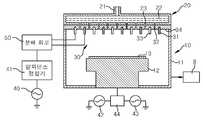
도 1은 본 발명의 바람직한 실시예예 따른 플라즈마 반응기의 단면도이다.1 is a cross-sectional view of a plasma reactor according to a preferred embodiment of the present invention.
도 1을 참조하여, 본 발명의 바람직한 실시예에 따른 혼합형 플라즈마 반응기는 플라즈마 반응기(10), 가스 공급부(20), 안테나 전극 어셈블리(30)를 포함한다. 플라즈마 반응기(10)는 내부에 피처리 기판(13)이 놓이는 지지대(12)가 구비된다. 플라즈마 반응기(10)의 상부에 안테나 전극 어셈블리(30)가 구성된다. 가스 공급부(20)는 안테나 전극 어셈블리(30)의 상부에 구성되어 가스 공원(미도시)으로부터 제공된 가스를 안테나 전극 어셈블리(30)의 가스 분사홀(32)을 통하여 플라즈마 반응기(10)의 내부로 공급한다. 메인 전원 공급원(40)으로부터 발생된 무선 주파수는 임피던스 정합기(41)와 분배 회로(50)를 통하여 안테나 전극 어셈블 리(30)에 안테나 전극(31, 33)으로 공급되어 플라즈마 반응기(10) 내부의 용량 결합된 플라즈마와 유도 결합된 플라즈마를 혼합적으로 유도한다. 플라즈마 반응기(10)의 내부에 발생된 혼합된 플라즈마에 의해 피처리 기판(13)에 대한 플라즈마 처리가 이루어진다.Referring to FIG. 1, a mixed plasma reactor according to a preferred embodiment of the present invention includes a
플라즈마 반응기(10)는 반응기 몸체(11)와 그 내부에 피처리 기판(13)이 놓이는 지지대(12)가 구비된다. 반응기 몸체(11)는 알루미늄, 스테인리스, 구리와 같은 금속 물질로 제작될 수 있다. 또는 코팅된 금속 예를 들어, 양극 처리된 알루미늄이나 니켈 도금된 알루미늄으로 제작될 수도 있다. 또는 내화 금속(refractory metal)로 제작될 수도 있다. 또 다른 대안으로 반응기 몸체(11)를 전체적 또는 부분적으로 석영, 세라믹과 같은 전기적 절연 물질로 제작하는 것도 가능하다. 이와 같이 반응기 몸체(11)는 의도된 플라즈마 프로세스가 수행되기에 적합한 어떠한 물질로도 제작될 수 있다. 반응기 몸체(11)의 구조는 피처리 기판(13)에 따라 그리고 플라즈마의 균일한 발생을 위하여 적합한 구조 예를 들어, 원형 구조나 사각형 구조 그리고 이외에도 어떠한 형태의 구조를 가질 수 있다.The
피처리 기판(13)은 예를 들어, 반도체 장치, 디스플레이 장치, 태양전지 등과 같은 다양한 장치들의 제조를 위한 웨이퍼 기판, 유리 기판, 플라스틱 기판 등과 같은 기판들이다. 플라즈마 반응기(10)는 진공 펌프(8)에 연결된다. 본 발명의 실시예에서 플라즈마 반응기(10)는 대기압 이하의 저압 상태에서 피처리 기판(13)에 대한 플라즈마 처리가 이루어진다. 그러나 본 발명의 용량 결합 플라즈마 반응기는 대기압에서 피처리 기판을 처리하는 대기압의 플라즈마 처리 시스템으 로도 그 사용이 가능하다.The
플라즈마 반응기(10)의 내부에는 피처리 기판(13)을 지지하기 위한 지지대(12)가 구비된다. 기판 지지대(12)는 바이어스 전원 공급원(42, 43)에 연결되어 바이어스 된다. 예를 들어, 서로 다른 무선 주파수 전원을 공급하는 두 개의 바이어스 전원 공급원(42, 43)이 임피던스 정합기(44)를 통하여 기판 지지대(12)에 전기적으로 연결되어 바이어스 된다. 기판 지지대(12)의 이중 바이어스 구조는 플라즈마 반응기(10)의 내부에 플라즈마 발생을 용이하게 하고, 플라즈마 이온 에너지 조절을 더욱 개선시켜 공정 생산력을 향상 시킬 수 있다. 또는 단일 바이어스 구조로 변형 실시할 수도 있다. 또는 지지대(12)는 바이어스 전원의 공급 없이 제로 퍼텐셜(zero potential)을 갖는 구조로 변형 실시될 수도 있다. 그리고 기판 지지대(12)는 정전척을 포함할 수 있다. 또는 기판 지지대(12)는 히터를 포함할 수 있다.A
가스 공급부(20)는 안테나 전극 어셈블리(30)의 상부에 설치된다. 가스 공급부(20)는 가스 공급원(미도시)에 연결되는 가스 입구(21)와 하나 이상의 가스 분배판(22) 그리고 복수개의 가스 주입구(23)를 구비한다. 복수개의 가스 주입구(23)는 전극 장착판(34)의 복수개의 가스 분사홀(32)에 대응되어 연결된다. 가스 입구(21)를 통하여 입력된 가스는 하나 이상의 가스 분배판(22)에 의해서 고르게 분배되어 복수개의 가스 주입구(23)와 그에 대응된 복수개의 가스 분사홀(32)을 통하여 플라즈마 반응기(10)의 내부로 고르게 분사된다. 구체적인 도면의 도시는 생략하였으나, 가스 공급부(20)는 둘 이상의 분리된 가스 공급 채널을 구비하여 서 로 다른 가스를 분리하여 플라즈마 반응기(10)의 내부로 공급할 수도 있다. 서로 다른 가스를 분리 공급하도록 하여 플라즈마 처리의 균일도를 높일 수 있다.The
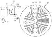
도 2는 안테나 전극 어셈블리와 분배 회로의 구성을 보여주는 도면이다.2 is a diagram illustrating a configuration of an antenna electrode assembly and a distribution circuit.
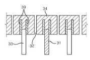
도 2를 참조하여, 안테나 전극 어셈블리(30)는 플라즈마 반응기(10)의 내부에 용량 결합된 플라즈마와 유도 결합된 플라즈마를 혼합적으로 유도하기 위한 복수개의 안테나 전극(31, 33)을 구비한다. 본 실시예에서는 두 개의 안테나 전극(31, 33)이 간격을 두고 이중 나선형으로 설치된 구조를 예시하고 있지만, 둘 이상의 복수개로 분할되어 설치될 수도 있다. 복수개의 안테나 전극(31, 33)은 반응기 몸체(11)의 내부 공간에 접하는 전극 장착판(34)의 일면에 장착된다. 전극 장착판(34)은 반응기 몸체(11)의 천정을 덮도록 설치될 수 있다. 안테나 전극(31, 33)은 전극 장착판(34)의 하부로 돌출된 나선형 장벽구조를 갖는다. 안테나 전극(31, 33)의 형상과 배치 구조는 다양한 변형이 가능하다.Referring to FIG. 2, the
전극 장착판(34)은 복수개의 가스 분사홀(32)을 구비한다. 복수개의 가스 분사홀(32)은 안테나 전극(31, 33) 사이를 따라서 일정 간격을 두고 형성된다. 전극 장착판(34)은 금속이나 비금속 또는 이들의 혼합된 물질로도 구성이 가능하다. 물론, 전극 장착판(34)이 금속 물질로 구성되는 경우에는 안테나 전극(31, 33)과의 사이에 전기적 절연 구조를 갖는다. 본 실시예에서 전극 장착판(34)과 안테나 전극(31, 33)은 반응기 몸체(11)의 천정에 구성되지만 플라즈마 처리 효율을 높이기 위하여 반응기 몸체(11)의 측벽을 따라서 설치될 수도 있다. 또는 천정과 측벽에 모두 설치될 수도 있다.The
안테나 전극(31, 33)은 메인 전원 공급원(40)으로부터 발생된 무선 주파수 전원을 임피던스 정합기(41)와 분배 회로(50)를 통하여 공급받아 구동되어 플라즈마 반응기(10) 내부의 용량 결합된 플라즈마와 유도 결합된 플라즈마를 발생시킨다. 메인 전원 공급원(40)은 별도의 임피던스 정합기 없이 출력 전원의 제어가 가능한 무선 주파수 발생기를 사용하여 구성될 수도 있다. 메인 전원 공급원(40)으로부터 제공되는 무선 주파수는 임피던스 정합기(41)를 통하여 분배 회로(50)로 제공되고, 분배 회로(50)는 안테나 전극(31, 33)으로 상호 전위차를 갖도록 무선 주파수의 위상을 달리하여 공급한다. 예를 들어, 분배 회로(50)는 접지된 중간탭(52)을 갖는 분할 코일(51)로 구성될 수 있다. 분할 코일(51)의 비반전 출력단(54)은 하나의 안테나 전극(33)으로 연결되고, 반전 출력단(56)은 다른 하나의 안테나 전극(31)으로 연결된다. 다른 변형예로서, 도 3에 도시된 바와 같이, 하나의 안테나 전극(33)은 임피던스 정합기(41)를 통하여 메인 전원 공급원(40)에 연결되고, 다른 하나의 안테나 전극(31)은 접지로 연결되도록 구성될 수도 있다. 안테나 전극 어셈블리(30)의 평면 구조도 원형의 구조를 갖거나 또는 도 4에 도시된 바와 같이 사각형의 구조를 가질 수 있으며, 각각의 구조에 따라 안테나 전극(31, 33)의 구조도 적절한 변형이 가능하다.The
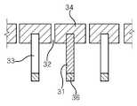
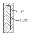
안테나 전극(31, 33)은, 도 5에 도시된 바와 같이, 둘 사이의 간격(a)이 높이(b) 이하 일 때 용량 결합 플라즈마 발생 효율이 높다. 안테나 전극(31, 33)은 기판 지지대(12)와의 직접적 용량 결합을 방지하기 위하여 기판 지지대(12)에 대향된 면으로 절연층(36)을 설치할 수 있다. 또는, 도 7에 도시된 바와 같이, 안테나 전극(31, 33)을 전체적으로 감싸는 절연층(37)을 설치할 수도 있다. 도 8에 도시된 바와 같이, 전극 장착판(34)은 안테나 전극(31, 33)의 과열을 막기 위하여 냉각 채널(38)을 구비할 수 있다.As shown in FIG. 5, the
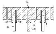
도 9a 및 도 9b는 안테나 전극의 방전 면적을 가변적으로 조절하기 위한 방전 면적 조절판을 설치한 예를 보여주는 도면이다.9A and 9B illustrate an example in which a discharge area control plate for variably adjusting the discharge area of an antenna electrode is installed.
도 9a 및 도 9b를 참조하여, 전극 장착판(34)은 안테나 전극(31, 33) 사이에 설치되어 용량 결합 방전 면적을 가변시키기 위한 방전 면적 조절판(39)을 구비할 수 있다. 방전 면적 조절판(39)은 상하로 이동 가능하도록 전극 장착판(34)에 설치되며, 하단으로 이동하는 정도에 따라서 안테나 전극(31, 33)의 용량 결합 방전 면적은 축소된다. 방전 면적이 축소되는 것에 따라서 용량 결합에 의한 플라즈마 발생 밀도가 감소됨으로 방전 면적 조절판(39)의 제어에 따라서 플라즈마 밀도를 제어할 수 있다. 방전 면적 조절판(39)은 안테나 전극(31, 33)의 전체에 걸쳐서 동일한 이동량을 가지도록 하거나 또는 복수개로 분할하여 각기 독립적으로 구동되도록 하여 지역적으로 서로 다른 이동량을 갖도록 할 수도 있다. 지역적으로 서로 다른 이동량을 갖는 경우에는 안테나 전극(31, 33)이 지역적으로 서로 다른 방전 면적을 갖게 되어 지역적인 플라즈마 밀도의 분할 제어가 가능하다.9A and 9B, the
이상에서 설명된 본 발명의 혼합형 플라즈마 반응기의 실시예는 예시적인 것에 불과하며, 본 발명이 속한 기술분야의 통상의 지식을 가진 자라면 이로부터 다양한 변형 및 균등한 타 실시예가 가능하다는 점을 잘 알 수 있을 것이다. 그럼으로 본 발명은 상기의 상세한 설명에서 언급되는 형태로만 한정되는 것은 아님을 잘 이해할 수 있을 것이다. 따라서 본 발명의 진정한 기술적 보호 범위는 첨부된 특허청구범위의 기술적 사상에 의해 정해져야 할 것이다. 또한, 본 발명은 첨부된 청구범위에 의해 정의되는 본 발명의 정신과 그 범위 내에 있는 모든 변형물과 균등물 및 대체물을 포함하는 것으로 이해되어야 한다.The embodiment of the mixed plasma reactor of the present invention described above is merely exemplary, and it is well understood that various modifications and equivalent other embodiments are possible to those skilled in the art to which the present invention pertains. Could be. Therefore, it will be understood that the present invention is not limited only to the form mentioned in the above detailed description. Therefore, the true technical protection scope of the present invention will be defined by the technical spirit of the appended claims. It is also to be understood that the present invention includes all modifications, equivalents, and substitutes within the spirit and scope of the invention as defined by the appended claims.
본 발명의 혼합형 플라즈마 반응기는 반도체 집적 회로의 제조, 평판 디스플레이 제조, 태양전지의 제조와 같은 다양한 박막 형성을 위한 플라즈마 처리 공정에 매우 유용하게 이용될 수 있다. The mixed plasma reactor of the present invention can be very usefully used in plasma processing processes for forming various thin films, such as fabrication of semiconductor integrated circuits, flat panel display fabrication, and solar cell fabrication.
도 1은 본 발명의 바람직한 실시예예 따른 플라즈마 반응기의 단면도이다.1 is a cross-sectional view of a plasma reactor according to a preferred embodiment of the present invention.
도 2는 안테나 전극 어셈블리와 분배 회로의 구성을 보여주는 도면이다.2 is a diagram illustrating a configuration of an antenna electrode assembly and a distribution circuit.
도 3은 안테나 전극 어셈블리의 전극 연결 구조를 변형한 예를 보여주는 도면이다.3 is a view showing a modified example of the electrode connection structure of the antenna electrode assembly.
도 4는 안테나 전극 어셈블리의 변형 구조를 보여주는 도면이다.4 is a view showing a modified structure of the antenna electrode assembly.
도 5는 안테나 전극의 설치 구조를 보여주는 도면이다.5 is a view showing the installation structure of the antenna electrode.
도 6은 안테나 전극의 밑단에 절연층을 설치한 예를 보여주는 도면이다.6 is a view showing an example in which an insulating layer is provided at the bottom of the antenna electrode.
도 7은 안테나 전극을 전체적으로 절연층으로 감싼 구조를 예시하는 도면이다.7 is a diagram illustrating a structure in which the antenna electrode is entirely covered with an insulating layer.
도 8은 전극 장착판에 안테나 전극을 냉각하기 위한 냉각 채널을 구비한 예를 보여주는 도면이다.8 is a view showing an example having a cooling channel for cooling the antenna electrode on the electrode mounting plate.
도 9a 및 도 9b는 안테나 전극의 방전 면적을 가변적으로 조절하기 위한 방전 면적 조절판을 설치한 예를 보여주는 도면이다.9A and 9B illustrate an example in which a discharge area control plate for variably adjusting the discharge area of an antenna electrode is installed.
*도면의 주요 부분에 대한 부호의 설명** Description of the symbols for the main parts of the drawings *
8: 진공 펌프10: 플라즈마 반응기8: vacuum pump 10: plasma reactor
11: 반응기 몸체12: 기판 지지대11: reactor body 12: substrate support
13: 피처리 기판20: 가스 공급부13: substrate to be processed 20: gas supply part
21: 가스 입구22: 가스 분배판21: gas inlet 22: gas distribution plate
23: 가스 주입구30: 안테나 전극 어셈블리23: gas inlet 30: antenna electrode assembly
31, 33: 안테나 전극32: 가스 분사홀31, 33: antenna electrode 32: gas injection hole
34: 전극 장착판36: 절연층34: electrode mounting plate 36: insulating layer
37: 절연층38: 냉각 채널37: insulation layer 38: cooling channel
39: 방전 면적 조절판40: 메인 전원 공급원39: discharge area control plate 40: main power supply
41: 임피던스 정합기42, 43: 바이어스 전원 공급원41:
44: 임피던스 정합기50: 분배 회로44: impedance matcher 50: distribution circuit
51: 분할 코일52: 중간탭51: split coil 52: middle tap
54: 비반전 출력단56: 반전 출력단54: non-inverted output stage 56: inverted output stage
Claims (12)
Translated fromKoreanPriority Applications (1)
| Application Number | Priority Date | Filing Date | Title |
|---|---|---|---|
| KR1020080042581AKR101002260B1 (en) | 2008-05-07 | 2008-05-07 | Mixed Plasma Reactor |
Applications Claiming Priority (1)
| Application Number | Priority Date | Filing Date | Title |
|---|---|---|---|
| KR1020080042581AKR101002260B1 (en) | 2008-05-07 | 2008-05-07 | Mixed Plasma Reactor |
Publications (2)
| Publication Number | Publication Date |
|---|---|
| KR20090116562A KR20090116562A (en) | 2009-11-11 |
| KR101002260B1true KR101002260B1 (en) | 2010-12-20 |
Family
ID=41601320
Family Applications (1)
| Application Number | Title | Priority Date | Filing Date |
|---|---|---|---|
| KR1020080042581AActiveKR101002260B1 (en) | 2008-05-07 | 2008-05-07 | Mixed Plasma Reactor |
Country Status (1)
| Country | Link |
|---|---|
| KR (1) | KR101002260B1 (en) |
Citations (1)
| Publication number | Priority date | Publication date | Assignee | Title |
|---|---|---|---|---|
| JP2001181848A (en) | 1999-12-20 | 2001-07-03 | Anelva Corp | Plasma processing equipment |
- 2008
- 2008-05-07KRKR1020080042581Apatent/KR101002260B1/enactiveActive
Patent Citations (1)
| Publication number | Priority date | Publication date | Assignee | Title |
|---|---|---|---|---|
| JP2001181848A (en) | 1999-12-20 | 2001-07-03 | Anelva Corp | Plasma processing equipment |
Also Published As
| Publication number | Publication date |
|---|---|
| KR20090116562A (en) | 2009-11-11 |
Similar Documents
| Publication | Publication Date | Title |
|---|---|---|
| KR100979186B1 (en) | Capacitively coupled plasma reactor | |
| KR20090125406A (en) | Mixed Plasma Reactor | |
| KR101496847B1 (en) | Inductively coupled plasma reactor | |
| KR100806522B1 (en) | Inductively coupled plasma reactor | |
| KR100980287B1 (en) | Inductively Coupled Plasma Reactor with Multiple Radio Frequency Antennas | |
| KR100864111B1 (en) | Inductively coupled plasma reactor | |
| KR101468730B1 (en) | Inductively Coupled Plasma Reactor with Multiple Radio Frequency Antennas | |
| KR20090009369A (en) | Plasma reactor with inductively coupled plasma source with heater | |
| KR101167952B1 (en) | Plasma reactor for generating large size plasma | |
| KR20100129368A (en) | Large Area Plasma Reactor Using Complex Frequency | |
| KR101585891B1 (en) | Compound plasma reactor | |
| KR20080028848A (en) | Inductively Coupled Plasma Reactor for Large Area Plasma Treatment | |
| KR101424487B1 (en) | Inductively coupled plasma reactor having multi rf antenna | |
| KR101384583B1 (en) | Inductively coupled plasma reactor having multi rf antenna | |
| KR20080070125A (en) | Inductively coupled plasma reactor | |
| KR100845917B1 (en) | Inductively Coupled Plasma Reactor for Large Area Plasma Treatment | |
| KR20100129373A (en) | Hybrid Plasma Reactor | |
| KR101236206B1 (en) | Inductively coupled plasma reactor for generating high density uniform plasma | |
| KR101112745B1 (en) | Plasma reactor have a variable capacitively coupled plasma | |
| KR101002260B1 (en) | Mixed Plasma Reactor | |
| KR20100129369A (en) | Large Area Plasma Reactor with Vertical Dual Chamber | |
| KR20100136857A (en) | Plasma Reactor with Multiple Plasma Generation Zones | |
| KR101383247B1 (en) | Method for etching thin film using advanced inductively coupled plasma source | |
| KR100753869B1 (en) | Hybrid Plasma Reactor | |
| KR101281191B1 (en) | Inductively coupled plasma reactor capable |
Legal Events
| Date | Code | Title | Description |
|---|---|---|---|
| PA0109 | Patent application | Patent event code:PA01091R01D Comment text:Patent Application Patent event date:20080507 | |
| A201 | Request for examination | ||
| PA0201 | Request for examination | Patent event code:PA02012R01D Patent event date:20080609 Comment text:Request for Examination of Application Patent event code:PA02011R01I Patent event date:20080507 Comment text:Patent Application | |
| PG1501 | Laying open of application | ||
| E902 | Notification of reason for refusal | ||
| PE0902 | Notice of grounds for rejection | Comment text:Notification of reason for refusal Patent event date:20100527 Patent event code:PE09021S01D | |
| E701 | Decision to grant or registration of patent right | ||
| PE0701 | Decision of registration | Patent event code:PE07011S01D Comment text:Decision to Grant Registration Patent event date:20101129 | |
| GRNT | Written decision to grant | ||
| PR0701 | Registration of establishment | Comment text:Registration of Establishment Patent event date:20101213 Patent event code:PR07011E01D | |
| PR1002 | Payment of registration fee | Payment date:20101213 End annual number:3 Start annual number:1 | |
| PG1601 | Publication of registration | ||
| FPAY | Annual fee payment | Payment date:20131213 Year of fee payment:4 | |
| PR1001 | Payment of annual fee | Payment date:20131213 Start annual number:4 End annual number:4 | |
| FPAY | Annual fee payment | Payment date:20141205 Year of fee payment:5 | |
| PR1001 | Payment of annual fee | Payment date:20141205 Start annual number:5 End annual number:5 | |
| FPAY | Annual fee payment | Payment date:20161213 Year of fee payment:7 | |
| PR1001 | Payment of annual fee | Payment date:20161213 Start annual number:7 End annual number:7 | |
| FPAY | Annual fee payment | Payment date:20171212 Year of fee payment:8 | |
| PR1001 | Payment of annual fee | Payment date:20171212 Start annual number:8 End annual number:8 | |
| FPAY | Annual fee payment | Payment date:20191210 Year of fee payment:10 | |
| PR1001 | Payment of annual fee | Payment date:20191210 Start annual number:10 End annual number:10 | |
| PR1001 | Payment of annual fee | Payment date:20201215 Start annual number:11 End annual number:11 | |
| PR1001 | Payment of annual fee | Payment date:20211214 Start annual number:12 End annual number:12 | |
| PR1001 | Payment of annual fee | Payment date:20241203 Start annual number:15 End annual number:15 |