KR100997983B1 - Mobile communication terminal - Google Patents
Mobile communication terminalDownload PDFInfo
- Publication number
- KR100997983B1 KR100997983B1KR1020080049044AKR20080049044AKR100997983B1KR 100997983 B1KR100997983 B1KR 100997983B1KR 1020080049044 AKR1020080049044 AKR 1020080049044AKR 20080049044 AKR20080049044 AKR 20080049044AKR 100997983 B1KR100997983 B1KR 100997983B1
- Authority
- KR
- South Korea
- Prior art keywords
- housing
- mobile communication
- communication terminal
- circuit board
- printed circuit
- Prior art date
- Legal status (The legal status is an assumption and is not a legal conclusion. Google has not performed a legal analysis and makes no representation as to the accuracy of the status listed.)
- Expired - Fee Related
Links
Images


Classifications
- H—ELECTRICITY
- H01—ELECTRIC ELEMENTS
- H01R—ELECTRICALLY-CONDUCTIVE CONNECTIONS; STRUCTURAL ASSOCIATIONS OF A PLURALITY OF MUTUALLY-INSULATED ELECTRICAL CONNECTING ELEMENTS; COUPLING DEVICES; CURRENT COLLECTORS
- H01R12/00—Structural associations of a plurality of mutually-insulated electrical connecting elements, specially adapted for printed circuits, e.g. printed circuit boards [PCB], flat or ribbon cables, or like generally planar structures, e.g. terminal strips, terminal blocks; Coupling devices specially adapted for printed circuits, flat or ribbon cables, or like generally planar structures; Terminals specially adapted for contact with, or insertion into, printed circuits, flat or ribbon cables, or like generally planar structures
- H01R12/70—Coupling devices
- H01R12/71—Coupling devices for rigid printing circuits or like structures
- H01R12/712—Coupling devices for rigid printing circuits or like structures co-operating with the surface of the printed circuit or with a coupling device exclusively provided on the surface of the printed circuit
- H01R12/716—Coupling device provided on the PCB
- H01R12/718—Contact members provided on the PCB without an insulating housing
- H—ELECTRICITY
- H01—ELECTRIC ELEMENTS
- H01Q—ANTENNAS, i.e. RADIO AERIALS
- H01Q1/00—Details of, or arrangements associated with, antennas
- H01Q1/12—Supports; Mounting means
- H01Q1/22—Supports; Mounting means by structural association with other equipment or articles
- H01Q1/24—Supports; Mounting means by structural association with other equipment or articles with receiving set
- H01Q1/241—Supports; Mounting means by structural association with other equipment or articles with receiving set used in mobile communications, e.g. GSM
- H01Q1/242—Supports; Mounting means by structural association with other equipment or articles with receiving set used in mobile communications, e.g. GSM specially adapted for hand-held use
- H01Q1/243—Supports; Mounting means by structural association with other equipment or articles with receiving set used in mobile communications, e.g. GSM specially adapted for hand-held use with built-in antennas
- H—ELECTRICITY
- H04—ELECTRIC COMMUNICATION TECHNIQUE
- H04B—TRANSMISSION
- H04B1/00—Details of transmission systems, not covered by a single one of groups H04B3/00 - H04B13/00; Details of transmission systems not characterised by the medium used for transmission
- H04B1/38—Transceivers, i.e. devices in which transmitter and receiver form a structural unit and in which at least one part is used for functions of transmitting and receiving
- H—ELECTRICITY
- H01—ELECTRIC ELEMENTS
- H01R—ELECTRICALLY-CONDUCTIVE CONNECTIONS; STRUCTURAL ASSOCIATIONS OF A PLURALITY OF MUTUALLY-INSULATED ELECTRICAL CONNECTING ELEMENTS; COUPLING DEVICES; CURRENT COLLECTORS
- H01R13/00—Details of coupling devices of the kinds covered by groups H01R12/70 or H01R24/00 - H01R33/00
- H01R13/02—Contact members
- H01R13/22—Contacts for co-operating by abutting
- H01R13/24—Contacts for co-operating by abutting resilient; resiliently-mounted
- H—ELECTRICITY
- H01—ELECTRIC ELEMENTS
- H01R—ELECTRICALLY-CONDUCTIVE CONNECTIONS; STRUCTURAL ASSOCIATIONS OF A PLURALITY OF MUTUALLY-INSULATED ELECTRICAL CONNECTING ELEMENTS; COUPLING DEVICES; CURRENT COLLECTORS
- H01R2101/00—One pole
- H—ELECTRICITY
- H01—ELECTRIC ELEMENTS
- H01R—ELECTRICALLY-CONDUCTIVE CONNECTIONS; STRUCTURAL ASSOCIATIONS OF A PLURALITY OF MUTUALLY-INSULATED ELECTRICAL CONNECTING ELEMENTS; COUPLING DEVICES; CURRENT COLLECTORS
- H01R2201/00—Connectors or connections adapted for particular applications
- H01R2201/02—Connectors or connections adapted for particular applications for antennas
- H—ELECTRICITY
- H01—ELECTRIC ELEMENTS
- H01R—ELECTRICALLY-CONDUCTIVE CONNECTIONS; STRUCTURAL ASSOCIATIONS OF A PLURALITY OF MUTUALLY-INSULATED ELECTRICAL CONNECTING ELEMENTS; COUPLING DEVICES; CURRENT COLLECTORS
- H01R2201/00—Connectors or connections adapted for particular applications
- H01R2201/16—Connectors or connections adapted for particular applications for telephony
- H—ELECTRICITY
- H04—ELECTRIC COMMUNICATION TECHNIQUE
- H04M—TELEPHONIC COMMUNICATION
- H04M1/00—Substation equipment, e.g. for use by subscribers
- H04M1/02—Constructional features of telephone sets
- H04M1/0202—Portable telephone sets, e.g. cordless phones, mobile phones or bar type handsets
- H04M1/026—Details of the structure or mounting of specific components
- H04M1/0274—Details of the structure or mounting of specific components for an electrical connector module
- H—ELECTRICITY
- H04—ELECTRIC COMMUNICATION TECHNIQUE
- H04M—TELEPHONIC COMMUNICATION
- H04M1/00—Substation equipment, e.g. for use by subscribers
- H04M1/02—Constructional features of telephone sets
- H04M1/0202—Portable telephone sets, e.g. cordless phones, mobile phones or bar type handsets
- H04M1/026—Details of the structure or mounting of specific components
- H04M1/0277—Details of the structure or mounting of specific components for a printed circuit board assembly
Landscapes
- Engineering & Computer Science (AREA)
- Computer Networks & Wireless Communication (AREA)
- Signal Processing (AREA)
- Telephone Set Structure (AREA)
- Support Of Aerials (AREA)
- Coupling Device And Connection With Printed Circuit (AREA)
Abstract
Translated fromKoreanDescription
Translated fromKorean본 발명은 이동통신 단말기에 관한 것으로서, 보다 상세하게는 이동통신 단말기의 하우징에 형성되는 필름형 안테나와 상기 하우징 내부의 인쇄회로 기판 사이의 안정적인 컨텍을 제공할 수 있는 이동통신 단말기에 관한 것이다.The present invention relates to a mobile communication terminal, and more particularly, to a mobile communication terminal capable of providing stable contact between a film-type antenna formed in a housing of a mobile communication terminal and a printed circuit board inside the housing.
최근들어, CDMA, PDA, DCS, GSM 등과 같은 다양한 대역을 별도로 사용하거나 또는 공용으로 사용하는 휴대용 무선 단말기가 빠르게 보급됨에 따라 다양한 기능과 디자인의 단말기가 등장하고 있다. 또한, 상기 단말기가 점차 소형화, 경박 단소화 되어감과 동시에 그 기능의 다양성이 더욱 부각되고 있는 실정이다. 따라서, 안테나의 기능을 유지하면서 단말기의 부피를 줄이는데 많은 관심이 모아지고 있다.Recently, portable wireless terminals using various bands such as CDMA, PDA, DCS, GSM, etc., or using them in common are rapidly spreading, and terminals with various functions and designs have emerged. In addition, as the terminal is gradually miniaturized and light and short, the variety of functions is more highlighted. Therefore, much attention has been paid to reducing the volume of the terminal while maintaining the function of the antenna.
특히 안테나 장치의 경우, 단말기의 외부로 일정길이만큼 돌출되도록 설치되는 로드 안테나 및 헬리컬 안테나는 전방향 방사로 인한 우수한 특성이 구현되는 반면, 단말기의 낙하시 파손될 수 있는 가장 취약한 부분이 되며, 휴대성을 저하시 키는 문제점을 야기시키게 된다. 따라서, 최근에는 안테나를 이동통신 단말기의 케이스와 일체로 형성하는 인몰딩 안테나에 대한 연구가 계속되고 있다.In particular, in the case of the antenna device, the rod antenna and the helical antenna, which are installed to protrude to the outside of the terminal by a predetermined length, have excellent characteristics due to omnidirectional radiation, while being the most vulnerable parts that can be damaged when the terminal falls. This can cause problems. Therefore, in recent years, research on the in-molding antenna which forms the antenna integrally with the case of the mobile communication terminal has been continued.
상기한 문제점을 해결하기 위해서 본 발명은, 이동통신 단말기의 하우징에 형성되는 필름형 안테나와 상기 하우징 내부의 인쇄회로 기판 사이의 안정적인 컨텍을 제공할 수 있는 이동통신 단말기를 제공하는 것을 목적으로 한다.In order to solve the above problems, an object of the present invention is to provide a mobile communication terminal that can provide a stable contact between the film-type antenna formed in the housing of the mobile communication terminal and the printed circuit board inside the housing.
본 발명은, 이동통신 단말기의 하우징과, 상기 하우징의 표면에 형성되는 필름형 안테나와, 상기 하우징의 내부에 배치되는 인쇄회로기판, 및 상기 필름형 안테나와 상기 인쇄회로기판을 전기적으로 연결하는 커넥터를 포함하는 이동통신 단말기를 제공할 수 있다.The present invention provides a housing for a mobile communication terminal, a film antenna formed on the surface of the housing, a printed circuit board disposed inside the housing, and a connector for electrically connecting the film antenna and the printed circuit board. It can provide a mobile communication terminal comprising a.
상기 필름형 안테나는, 인몰딩 공정에 의해 상기 하우징과 일체로 형성될 수 있다.The film antenna may be integrally formed with the housing by an in-molding process.
상기 커넥터는, 인몰딩 공정에 의해 상기 하우징에 일부가 삽입된 형태로 형성될 수 있다.The connector may be formed in a form in which a part is inserted into the housing by an in-molding process.
상기 커넥터는, 상기 필름형 안테나와 접촉하는 제1 컨텍부와, 상기 인쇄회로 기판에 연결되는 제2 컨텍부, 및 상기 제1 컨텍부와 제2 컨텍부 사이에 형성되 어 상기 커넥터를 상기 하우징에 지지하는 지지부를 포함할 수 있다.The connector is formed between the first contact portion in contact with the film antenna, the second contact portion connected to the printed circuit board, and the first contact portion and the second contact portion to connect the connector to the housing. It may include a support for supporting.
상기 제1 컨텍부는, 탄성을 갖도록 절곡부가 형성될 수 있다.The first contact portion may have a bent portion to have elasticity.
상기 제2 컨텍부는, 상기 인쇄회로 기판에 형성된 비아홀을 통과하여, 상기 인쇄회로 기판에서 상기 필름형 안테나에 대향하는 면의 배면에 납땜될 수 있다.The second contact part may be soldered to a rear surface of the printed circuit board facing the film antenna through the via hole formed in the printed circuit board.
상기 지지부는, 상기 제1 컨텍부와 상기 제2 컨텍부를 연결하는 제1 지지부, 및 상기 수직 지지부에서 연장되는 제2 지지부를 포함할 수 있다.The support part may include a first support part connecting the first contact part and the second contact part, and a second support part extending from the vertical support part.
상기 제1 지지부는, 상기 인쇄회로 기판의 주면에 수직일 수 있다.The first support part may be perpendicular to a main surface of the printed circuit board.
상기 제2 지지부는, 상기 인쇄회로 기판의 주면에 수평일 수 있다.The second support part may be horizontal to a main surface of the printed circuit board.
상기 하우징은, 상기 지지부를 지지하기 위한 돌출영역을 포함할 수 있다.The housing may include a protruding region for supporting the support.
본 발명에 따르면, 이동통신 단말기의 하우징에 형성되는 필름형 안테나와 상기 하우징 내부의 인쇄회로 기판 사이의 안정적인 컨텍을 제공할 수 있다.According to the present invention, it is possible to provide stable contact between the film-type antenna formed in the housing of the mobile communication terminal and the printed circuit board inside the housing.
이하, 첨부된 도면을 참조하여 본 발명을 상세히 설명하겠다.Hereinafter, with reference to the accompanying drawings will be described in detail the present invention.
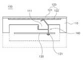
도 1은, 본 발명의 일실시 형태에 따른 이동통신 단말기의 단면도이다.1 is a cross-sectional view of a mobile communication terminal according to one embodiment of the present invention.
도 1을 참조하면, 본 실시형태에 따른 이동통신 단말기(100)는, 이동통신 단말기의 하우징(110), 필름형 안테나(120), 인쇄회로 기판(130), 및 커넥터(140)를 포함할 수 있다.Referring to FIG. 1, the
상기 필름형 안테나(120)는, 캐리어 필름(121) 및 도전패턴(122)을 포함할 수 있다.The
상기 캐리어 필름(121)은 인몰딩 라벨링(IML:In Molding Labelling)공정에 적합한 물질이 사용될 수 있다. 인몰딩 라벨링 공정을 보다 구체적으로 설명하면, 상기 도전패턴(122)이 일면에 형성된 캐리어 필름(121)을 이동통신단말기의 하우징을 제조하기 위한 금형틀 내에 삽입시키고, 상기 금형틀에 이동통신 단말기의 하우징을 구성할 합성수지를 주입하면서 적정 온도와 적정 압력에서 성형할 수 있다. 따라서, 상기 캐리어 필름(121)을 구성하는 물질은 상기 인몰딩공정시의 압력과 온도에 의해서 큰 변형이 발생되지 않으면서 이동통신단말기의 하우징에 일체화될 수 있는 물질을 사용하는 것이 요구된다. 본 실시형태에서 상기 캐리어 필름(121)은 얇은 절연성 폴리머물질을 포함할 수 있다.The
상기 도전패턴(122)은, 상기 캐리어 필름(121)의 일면에 형성되는 안테나 패턴일 수 있다.The
상기 도전패턴(122)을 형성하는 방법은 다양하게 구현될 수 있다. 먼저, 상기 캐리어 필름(121)상에 도전성 잉크를 사용하여 도전패턴을 인쇄할 수 있다. 또는, 스퍼터링이나 증착 공정을 통해 직접 원하는 패턴을 상기 캐리어 필름 상에 형성할 수 있다. 상기 도전패턴(122)은 미리 제조된 금속박으로 된 도체패턴을 상기 캐리어 필름(121)에 부착되어 형성될 수 있다.The
상기 도전 패턴(122)은 급전단을 포함하며, 추가적으로 접지단과 같이 외부 회로와 접속을 위한 연결단을 포함할 수 있다. 본 실시형태에서는 상기 급전단이 상기 커넥터(140)와 접촉되는 컨텍영역이 될 수 있다.The
상기 이동통신 단말기의 하우징(110)은, 인몰딩 공정에 의해 형성될 수 있다. 즉, 도전패턴이 형성된 캐리어 필름을 하우징 제작을 위한 몰드 내에 삽입시키고, 상기 하우징을 형성하기 위한 합성수지를 상기 몰드 내에 주입하여 상기 하우징이 제조될 수 있다. 본 실시형태에서, 상기 캐리어 필름(121)은 상기 하우징(110)과 일체화되어 상기 하우징의 표면에 형성될 수 있다.The
본 실시형태에서, 상기 캐리어 필름(121)은 상기 하우징(110)의 외부 표면에 형성될 수 있다. 상기 하우징(110)과 캐리어 필름(121) 사이에는 도전패턴(122)이 위치할 수 있다.In this embodiment, the
상기 하우징의 형태는 다양하게 구현될 수 있으며, 본 실시형태에서 상기 하우징(110)의 내부에는 커넥터(140)를 지지하기 위한 돌출영역(111)이 형성될 수 있다. 상기 돌출영역의 형태나 위치는 커넥터의 형태나 위치에 따라 다양하게 구현 될 수 있다.The housing may have various shapes, and in the present embodiment, a
상기 인쇄회로 기판(130)은, 이동통신 단말기의 하우징 내부에 배치될 수 있다. 상기 인쇄회로 기판(130)에는 복수개의 능동소자 및 수동소자가 실장될 수 있다. 상기 인쇄회로 기판에는 상기 필름형 안테나(120)에 전류를 공급하기 위한 급전라인이 형성될 수 있다.The printed
본 실시형태에서는, 상기 인쇄회로 기판(130)에 비아홀이 형성될 수 있으며, 상기 커넥터(140)의 일단이 상기 비아홀을 관통하도록 배치될 수 있다. 상기 커넥터의 일단은 상기 인쇄회로 기판의 주면 중 상기 필름형 안테나와 대향하는 면의 배면에서 납땜에 의해 상기 급전부에 연결될 수 있다.In the present exemplary embodiment, a via hole may be formed in the printed
상기 커넥터(140)는, 상기 필름형 안테나(120)와 상기 인쇄회로 기판(130)을 연결할 수 있다. 즉, 상기 커넥터(140)는 이동통신 단말기 하우징의 표면에 형성된 상기 필름형 안테나의 도전패턴(122)에 일단이 접촉되고, 상기 이동통신 단말기 하우징의 내부에 배치되는 인쇄회로 기판(130)의 급전라인에 타단이 접촉될 수 있다.The
본 실시형태에서는, 상기 커넥터(140)는 상기 이동통신 단말기의 하우징(110)과 일체로 형성될 수 있다. 상기 하우징(110)을 제조하는 공정은 인몰딩 공정이 사용될 수 있다. 즉, 인몰딩 공정시 상기 커넥터를 하우징 제작을 위한 몰드 내에 삽입시키고, 상기 하우징을 형성하기 위한 합성수지를 상기 몰드 내에 주입하여 상기 하우징이 제조될 수 있다. 이 때, 상기 커넥터(140)는 상기 하우징(110)과 일체화되어 커넥터의 일부가 상기 하우징에 내부에 삽입된 형태로 형성될 수 있다.In this embodiment, the
본 실시형태에서는, 상기 커넥터의 타단은 인쇄회로 기판에 형성된 비아홀을 통과하여 상기 인쇄회로 기판의 배면에 납땜될 수 있다. 이처럼, 커넥터를 인쇄회로 기판의 주면 중 상기 필름형 안테나에 대향하는 면에 납땜하지 않고, 상기 필름형 안테나에 대향하는 면의 배면에 납땜부(131)를 형성함으로써, 상기 인쇄회로 기판(130)과 커넥터(140) 사이의 결합을 견고하게 할 수 있다.In the present embodiment, the other end of the connector can be soldered to the back surface of the printed circuit board through the via hole formed in the printed circuit board. In this way, the soldering
도 2는, 본 발명의 일실시 형태에 따른 이동통신 단말기에 사용되는 커넥터의 사시도이다.2 is a perspective view of a connector used in the mobile communication terminal according to the embodiment of the present invention.
본 실시형태에 따른 커넥터(240)는, 제1 컨텍부(241), 제2 컨텍부(242), 및 지지부(243)를 포함할 수 있다.The
상기 제1 컨텍부(241)는 이동통신 단말기의 하우징에 형성된 필름형 안테나의 도전패턴에 접촉될 수 있다.The
상기 제1 컨텍부(241)에는 적어도 하나의 절곡부(241a)가 형성될 수 있다. 상기 절곡부를 형성함으로써 상기 컨텍부는 소정의 탄성을 가질 수 있다. 이처럼 탄성을 갖도록 제1 컨텍부를 형성하면, 상기 제1 컨텍부(241)가 필름형 안테나와 접촉시 제1 컨텍부에 의해 필름형 안테나의 형태가 변하는 것을 방지할 수 있다.At least one
상기 제2 컨텍부(242)는, 이동통신 단말기의 하우징 내부에 배치된 인쇄회로 기판에 연결될 수 있다. 상기 제2 컨텍부(242)는 납땜에 의해 인쇄회로 기판에 형성된 급전라인에 전기적으로 연결될 수 있다. 상기 납땜에 의해 상기 커넥터를 인 쇄회로 기판에 고정시킬 수 있다. 본 실시형태에서는 상기 제2 컨텍부(242)는 인쇄회로 기판의 배면에 납땜될 수 있다. 따라서, 상기 제2 컨텍부(242)는 인쇄회로 기판에 형성된 비아홀을 관통할 수 있도록 형성될 수 있다.The
상기 지지부(243)은, 상기 제1 컨텍부(241)와 제2 컨텍부(242) 사이에 형성되며, 상기 커넥터를 이동통신 단말기의 하우징에 지지시킬 수 있다.The
본 실시형태에서, 상기 지지부(243)는 제1 지지부(243-1), 제2 지지부(243-2), 제3 지지부(243-3)를 포함할 수 있다. 상기 제1 지지부(243-1)은 상기 제1 컨텍부(241)와 제2 컨텍부(242)를 직접 연결할 수 있다. 상기 커넥터를 이동통신 단말기의 하우징 내에 배치할 때, 상기 제1 지지부(243-1)는 상기 커넥터가 연결되는 인쇄회로 기판의 주면에 수직으로 배치될 수 있다.In this embodiment, the
상기 제2 지지부(243-2)는, 상기 제1 지지부(243-1)에서 연장될 수 있다. 상기 제2 지지부(243-2)는 상기 제1 지지부(243-1)와 수직으로 연결될 수 있다. 이 경우, 상기 커넥터를 이동통신 단말기의 하우징 내에 배치할 때, 상기 제2 지지부(243-2)는 상기 커넥터가 연결되는 인쇄회로 기판의 주면에 대해 평행하게 배치될 수 있다.The second support part 243-2 may extend from the first support part 243-1. The second support part 243-2 may be vertically connected to the first support part 243-1. In this case, when the connector is disposed in the housing of the mobile communication terminal, the second support portion 243-2 may be disposed in parallel with the main surface of the printed circuit board to which the connector is connected.
상기 제3 지지부(243-3)는 상기 제2 지지부(243-2)에서 연장될 수 있다. 상기 제3 지지부(243-3)는 상기 제2 지지부(243-2)와 수직으로 연결될 수 있다.The third supporter 243-3 may extend from the second supporter 243-2. The third supporter 243-3 may be vertically connected to the second supporter 243-2.
본 실시형태에서, 서로 수직으로 연결되는 제1 지지부(243-1), 제2 지지부(243-2), 및 제3 지지부(243-3)는, 상기 커넥터가 결합되는 이동통신 단말기의 하우징의 일부와 밀착되어 상기 커넥터를 견고하게 지지할 수 있다. 상기 지지부를 보다 견고하게 지지하기 위해서 이동통신 단말기의 내부에는 돌출영역이 형성될 수 있다.In the present embodiment, the first support portion 243-1, the second support portion 243-2, and the third support portion 243-3, which are vertically connected to each other, are formed of the housing of the mobile communication terminal to which the connector is coupled. In close contact with the part, the connector can be firmly supported. In order to support the support more firmly, a protruding region may be formed inside the mobile communication terminal.
도 3의 (a) 내지 (c)는, 본 발명의 일실시 형태에 따른 이동통신 단말기를 제조하는 공정의 순서도이다.3A to 3C are flowcharts of a process of manufacturing a mobile communication terminal according to one embodiment of the present invention.
도 3의 (a)는, 인몰딩 공정을 수행하기 위해서 필름형 안테나 및 커넥터를 이동통신 단말기의 하우징의 형태를 갖는 몰드 내에 위치시키는 공정이다. 본 도면에서는 몰드의 구체적인 형태는 생략하였다.3A illustrates a process of placing a film-type antenna and a connector in a mold having a housing shape of a mobile communication terminal in order to perform an in-molding process. In this figure, the specific form of the mold is omitted.
상기 필름형 안테나(320)는 캐리어 필름(321) 상에 도전패턴(322)이 형성될 수 있다. 상기 캐리어 필름(321)은 인몰딩 라벨링(IML:In Molding Labelling)공정에 적합한 물질이 사용될 수 있다. 인몰딩 라벨링 공정을 보다 구체적으로 설명하면, 상기 도전패턴(322)이 일면에 형성된 캐리어 필름(321)을 이동통신단말기의 하우징을 제조하기 위한 금형틀 내에 삽입시키고, 상기 금형틀에 이동통신 단말기의 하우징을 구성할 합성수지를 주입하면서 적정 온도와 적정 압력에서 성형할 수 있다. 따라서, 상기 캐리어 필름(321)을 구성하는 물질은 상기 인몰딩공정시의 압력과 온도에 의해서 큰 변형이 발생되지 않으면서 이동통신단말기의 하우징에 일체화될 수 있는 물질을 사용하는 것이 요구된다. 본 실시형태에서 상기 캐리어 필름(321)은 얇은 절연성 폴리머물질을 포함할 수 있다.In the
상기 도전패턴(322)은, 상기 캐리어 필름(321)의 일면에 형성되는 안테나 패턴일 수 있다. 상기 도전패턴(322)을 형성하는 방법은 다양하게 구현될 수 있다. 먼저, 상기 캐리어 필름(321)상에 도전성 잉크를 사용하여 도전패턴을 인쇄할 수 있다. 또는, 스퍼터링이나 증착 공정을 통해 직접 원하는 패턴을 상기 캐리어 필름 상에 형성할 수 있다. 상기 도전패턴(322)은 미리 제조된 금속박으로 된 도체패턴을 상기 캐리어 필름(321)에 부착되어 형성될 수 있다. 상기 도전 패턴(322)은 급전단을 포함하며, 추가적으로 접지단과 같이 외부 회로와 접속을 위한 연결단을 포함할 수 있다. 본 실시형태에서는 상기 급전단이 상기 커넥터(340)와 접촉되는 컨텍영역이 될 수 있다.The
상기 커넥터(340)는 도전성 물질로 이루어질 수 있다. 상기 커넥터의 일단은 상기 도전패턴(322)에 접촉되도록 배치될 수 있다.The
도 3의 (b)는, 상기 몰드 내에 이동통신 단말기의 하우징을 구성하는 합성수지를 주입하여 하우징을 형성하는 공정이다.3B is a step of forming a housing by injecting a synthetic resin constituting the housing of the mobile communication terminal into the mold.
상기 이동통신 단말기의 하우징(310)은, 인몰딩 공정에 의해 형성될 수 있다. 즉, 필름형 안테나(320) 및 커넥터(340)를 하우징 제작을 위한 몰드 내에 삽입시키고, 하우징을 형성하기 위한 합성수지를 상기 몰드 내에 주입하여 상기 하우징이 제조될 수 있다. 이 때, 상기 필름형 안테나(320)는 상기 하우징(310)과 일체화되어 상기 하우징의 표면에 형성되고, 상기 커넥터(340)는 일부가 상기 하우징에 삽입되어 고정될 수 있다.The
본 실시형태에서, 상기 필름형 안테나(320)는 상기 하우징(310)의 외부 표면에 형성될 수 있다. 상기 커넥터(340)를 지지하기 위해서 상기 하우징(310)에는 돌 출영역(311)이 형성될 수 있다.In this embodiment, the
도 3의 (c)는, 하우징의 내부에 인쇄회로 기판(330)을 배치하고 상기 커넥터(340)를 인쇄회로 기판에 연결하는 공정이다.3C illustrates a process of disposing a printed
상기 커넥터(340)의 일단을 상기 인쇄회로기판에 형성된 비아홀에 삽입하고, 상기 인쇄회로 기판의 배면에서 상기 커넥터를 상기 인쇄회로 기판에 형성된 급전라인에 납땜할 수 있다. 상기 납땜에 의해 커넥터와 인쇄회로 기판의 급전라인 사이에 전기적인 연결이 되고, 또한 물리적인 결합력을 강화시킬 수 있다.One end of the
본 도면에서는, 하우징의 일부에 대해서만 도시하였으나, 상기 하우징(310)에 대응하는 하우징이 결합되어 이동통신 단말기가 제조될 수 있다.In the drawing, only a part of the housing is illustrated, but a housing corresponding to the
본 발명은 상술한 실시형태 및 첨부된 도면에 의해 한정되는 것이 아니며, 첨부된 청구범위에 의해 한정하고자 한다. 따라서, 청구범위에 기재된 본 발명의 기술적 사상을 벗어나지 않는 범위 내에서 당 기술분야의 통상의 지식을 가진 자에 의해 다양한 형태의 치환, 변형 및 변경이 가능할 것이며, 이 또한 본 발명의 범위에 속한다고 할 것이다.It is intended that the invention not be limited by the foregoing embodiments and the accompanying drawings, but rather by the claims appended hereto. It will be apparent to those skilled in the art that various changes in form and details may be made therein without departing from the spirit and scope of the invention as defined by the appended claims. something to do.
도 1은, 본 발명의 일실시 형태에 따른 이동통신 단말기의 단면도이다.1 is a cross-sectional view of a mobile communication terminal according to one embodiment of the present invention.
도 2는, 본 발명의 일실시 형태에 따른 이동통신 단말기에 사용되는 커넥터의 사시도이다.2 is a perspective view of a connector used in the mobile communication terminal according to the embodiment of the present invention.
도 3의 (a) 내지 (c)는, 본 발명의 일실시 형태에 따른 이동통신 단말기를 제조하는 공정의 순서도이다.3A to 3C are flowcharts of a process of manufacturing a mobile communication terminal according to one embodiment of the present invention.
<도면의 주요 부분에 대한 부호설명><Code Description of Main Parts of Drawing>
110 : 하우징 120 : 필름형 안테나110
130 : 인쇄회로 기판140 : 커넥터130: printed circuit board 140: connector
Claims (10)
Translated fromKoreanPriority Applications (4)
| Application Number | Priority Date | Filing Date | Title |
|---|---|---|---|
| KR1020080049044AKR100997983B1 (en) | 2008-05-27 | 2008-05-27 | Mobile communication terminal |
| US12/243,697US7973727B2 (en) | 2008-05-27 | 2008-10-01 | Mobile communication terminal |
| CNA2008101667572ACN101594400A (en) | 2008-05-27 | 2008-10-23 | Mobile communication terminal |
| DE102008052987ADE102008052987A1 (en) | 2008-05-27 | 2008-10-23 | Mobile communication terminal |
Applications Claiming Priority (1)
| Application Number | Priority Date | Filing Date | Title |
|---|---|---|---|
| KR1020080049044AKR100997983B1 (en) | 2008-05-27 | 2008-05-27 | Mobile communication terminal |
Publications (2)
| Publication Number | Publication Date |
|---|---|
| KR20090123123A KR20090123123A (en) | 2009-12-02 |
| KR100997983B1true KR100997983B1 (en) | 2010-12-03 |
Family
ID=41335049
Family Applications (1)
| Application Number | Title | Priority Date | Filing Date |
|---|---|---|---|
| KR1020080049044AExpired - Fee RelatedKR100997983B1 (en) | 2008-05-27 | 2008-05-27 | Mobile communication terminal |
Country Status (4)
| Country | Link |
|---|---|
| US (1) | US7973727B2 (en) |
| KR (1) | KR100997983B1 (en) |
| CN (1) | CN101594400A (en) |
| DE (1) | DE102008052987A1 (en) |
Families Citing this family (24)
| Publication number | Priority date | Publication date | Assignee | Title |
|---|---|---|---|---|
| SE530778C2 (en)* | 2006-12-08 | 2008-09-09 | Perlos Oyj | Antenna device |
| KR20090006336A (en)* | 2007-07-11 | 2009-01-15 | 삼성전기주식회사 | Case integrated antenna and manufacturing method |
| KR101018130B1 (en)* | 2008-12-02 | 2011-02-25 | 삼성전기주식회사 | Mobile communication terminal case and its manufacturing method |
| KR100945117B1 (en)* | 2009-04-23 | 2010-03-02 | 삼성전기주식회사 | Antenna pattern frame, method for manufacturing the same |
| KR100935954B1 (en) | 2009-04-23 | 2010-01-12 | 삼성전기주식회사 | Case of electronic device, method and mould for manufacturing the same, and mobile communication terminal |
| KR100945123B1 (en) | 2009-04-23 | 2010-03-02 | 삼성전기주식회사 | Antenna pattern frame, method and mould for manufacturing the same,and electronic device |
| TWI521787B (en)* | 2009-10-09 | 2016-02-11 | 宏達國際電子股份有限公司 | Handheld device and disposition method of planar antenna |
| TW201115823A (en)* | 2009-10-23 | 2011-05-01 | Wistron Corp | Antenna manufacturing method |
| TWI552429B (en)* | 2010-06-25 | 2016-10-01 | 泰科資訊科技有限公司 | Antenna device and its manufacturing method |
| DE102010061351A1 (en)* | 2010-12-20 | 2012-06-21 | Huf Hülsbeck & Fürst Gmbh & Co. Kg | Compact, NFC communication option having ID transmitter of a motor vehicle access system |
| US8791864B2 (en)* | 2011-01-11 | 2014-07-29 | Apple Inc. | Antenna structures with electrical connections to device housing members |
| TWM411099U (en)* | 2011-04-18 | 2011-09-01 | Chi Mei Comm Systems Inc | Electromagnetic shielding |
| KR101808862B1 (en)* | 2011-12-16 | 2018-01-19 | 삼성전자주식회사 | Ground devic and portable terminal having the same |
| TW201328019A (en)* | 2011-12-28 | 2013-07-01 | Hon Hai Prec Ind Co Ltd | Antenna frame |
| US9077794B2 (en)* | 2012-09-27 | 2015-07-07 | Tyfone, Inc. | Lightning connector accessory device |
| KR101978242B1 (en)* | 2012-12-21 | 2019-05-14 | 삼성전자주식회사 | Electronic device |
| JP6099471B2 (en)* | 2013-04-25 | 2017-03-22 | シャープ株式会社 | Portable device |
| KR101436737B1 (en)* | 2013-05-02 | 2014-09-02 | 에이큐 주식회사 | Connector |
| KR101550061B1 (en)* | 2014-03-04 | 2015-09-04 | 주식회사 핀크래프트엔지니어링 | Hybrid Type Antenna Radiator and the Manufacturing Method of the Same |
| KR20160030594A (en)* | 2014-09-03 | 2016-03-21 | 삼성전기주식회사 | Radiator frame having antenna pattern therein and manufacturing method of the same |
| CN104733888B (en)* | 2015-03-11 | 2017-07-07 | 东莞劲胜精密组件股份有限公司 | Built-in antenna connector and mobile terminal device |
| TWI659678B (en)* | 2015-09-15 | 2019-05-11 | 大陸商東莞錢鋒特殊膠黏製品有限公司 | Antenna composite molding structure of mobile electronic device and manufacturing method thereof |
| CN106099451B (en)* | 2016-06-14 | 2018-08-21 | 深圳市信维通信股份有限公司 | Shrapnel connection structure and preparation method thereof |
| CN106331235A (en)* | 2016-09-12 | 2017-01-11 | 努比亚技术有限公司 | Mobile terminal main board, mobile terminal main board setting method, and mobile terminal |
Citations (1)
| Publication number | Priority date | Publication date | Assignee | Title |
|---|---|---|---|---|
| WO2002073737A1 (en) | 2001-03-13 | 2002-09-19 | Gigaant Ab | Antenna device |
Family Cites Families (8)
| Publication number | Priority date | Publication date | Assignee | Title |
|---|---|---|---|---|
| US5258892A (en) | 1992-01-22 | 1993-11-02 | Motorola, Inc. | Molded-in antenna with solderless interconnect |
| JP2002329541A (en) | 2001-05-01 | 2002-11-15 | Kojima Press Co Ltd | Contact for antenna signal |
| JP4081675B2 (en) | 2003-04-22 | 2008-04-30 | 日本電気株式会社 | Auxiliary antenna mounting structure, wireless device, antenna unit, and ground mounting structure |
| KR200356488Y1 (en) | 2004-04-01 | 2004-07-15 | 주식회사 이엠따블유안테나 | Structure for contacting internal antenna terminal |
| JP4633605B2 (en)* | 2005-01-31 | 2011-02-16 | 富士通コンポーネント株式会社 | ANTENNA DEVICE AND ELECTRONIC DEVICE, ELECTRONIC CAMERA, ELECTRONIC CAMERA LIGHT EMITTING DEVICE, AND PERIPHERAL DEVICE |
| CA2619743C (en) | 2005-08-16 | 2013-09-17 | Suntory Limited | Oligonucleotides, arrays thereof for detecting microorganisms, and an apparatus, a method and a kit for detecting microorganisms |
| JP4102411B2 (en)* | 2006-04-13 | 2008-06-18 | 株式会社東芝 | Mobile communication terminal |
| KR100832849B1 (en) | 2006-07-20 | 2008-05-29 | 주식회사 유뎀 | Mobile communication terminal |
- 2008
- 2008-05-27KRKR1020080049044Apatent/KR100997983B1/ennot_activeExpired - Fee Related
- 2008-10-01USUS12/243,697patent/US7973727B2/ennot_activeExpired - Fee Related
- 2008-10-23CNCNA2008101667572Apatent/CN101594400A/enactivePending
- 2008-10-23DEDE102008052987Apatent/DE102008052987A1/ennot_activeCeased
Patent Citations (1)
| Publication number | Priority date | Publication date | Assignee | Title |
|---|---|---|---|---|
| WO2002073737A1 (en) | 2001-03-13 | 2002-09-19 | Gigaant Ab | Antenna device |
Also Published As
| Publication number | Publication date |
|---|---|
| CN101594400A (en) | 2009-12-02 |
| DE102008052987A1 (en) | 2009-12-24 |
| KR20090123123A (en) | 2009-12-02 |
| US7973727B2 (en) | 2011-07-05 |
| US20090295649A1 (en) | 2009-12-03 |
Similar Documents
| Publication | Publication Date | Title |
|---|---|---|
| KR100997983B1 (en) | Mobile communication terminal | |
| KR101153673B1 (en) | Sim card assembly, method for manufacturing the same, and electronic device including the same | |
| KR100961137B1 (en) | Mobile communication terminal case and its manufacturing method | |
| US9035847B2 (en) | Antenna pattern frame and mold for manufacturing electronic device case including the same | |
| KR20090121973A (en) | Film Antenna and Mobile Terminal | |
| CN105048083A (en) | Antenna pattern frame and method of manufacturing the same | |
| KR101138646B1 (en) | The Antenna integrated with housing of mobile phone and fabricating method thereof | |
| KR101333114B1 (en) | Wire type built-in antenna for portable terminal and manufacturing method of the same | |
| KR20100016841A (en) | Mobile communication terminal case and mobile communication terminal | |
| CN113363702B (en) | Antenna device and wireless earphone | |
| JP3618671B2 (en) | Interface connector | |
| KR100849805B1 (en) | Built-in antenna and built-in antenna manufacturing method | |
| KR100826392B1 (en) | Mobile device and manufacturing method thereof | |
| KR20100090574A (en) | Injection mold for embedded antenna | |
| KR101018130B1 (en) | Mobile communication terminal case and its manufacturing method | |
| KR100878393B1 (en) | Antenna structures | |
| KR101123792B1 (en) | Contact structure for internal antenna and mobile communication device comprising the same | |
| KR20170084794A (en) | Antenna Module | |
| KR100839688B1 (en) | Built-in antenna | |
| KR20090063939A (en) | Built-in antenna manufacturing method | |
| KR20080033593A (en) | Built-in antenna for wireless terminal | |
| JPH10190512A (en) | Portable radio | |
| KR100530160B1 (en) | The Connector Apparatus for Card in mobile phone | |
| KR100891792B1 (en) | Built-in antenna device for mobile communication terminal | |
| KR100580778B1 (en) | Mountable PC antenna and manufacturing method of mounted PC antenna |
Legal Events
| Date | Code | Title | Description |
|---|---|---|---|
| A201 | Request for examination | ||
| PA0109 | Patent application | St.27 status event code:A-0-1-A10-A12-nap-PA0109 | |
| PA0201 | Request for examination | St.27 status event code:A-1-2-D10-D11-exm-PA0201 | |
| D13-X000 | Search requested | St.27 status event code:A-1-2-D10-D13-srh-X000 | |
| D14-X000 | Search report completed | St.27 status event code:A-1-2-D10-D14-srh-X000 | |
| PG1501 | Laying open of application | St.27 status event code:A-1-1-Q10-Q12-nap-PG1501 | |
| E902 | Notification of reason for refusal | ||
| PE0902 | Notice of grounds for rejection | St.27 status event code:A-1-2-D10-D21-exm-PE0902 | |
| E13-X000 | Pre-grant limitation requested | St.27 status event code:A-2-3-E10-E13-lim-X000 | |
| P11-X000 | Amendment of application requested | St.27 status event code:A-2-2-P10-P11-nap-X000 | |
| P13-X000 | Application amended | St.27 status event code:A-2-2-P10-P13-nap-X000 | |
| E701 | Decision to grant or registration of patent right | ||
| PE0701 | Decision of registration | St.27 status event code:A-1-2-D10-D22-exm-PE0701 | |
| GRNT | Written decision to grant | ||
| PR0701 | Registration of establishment | St.27 status event code:A-2-4-F10-F11-exm-PR0701 | |
| PR1002 | Payment of registration fee | St.27 status event code:A-2-2-U10-U11-oth-PR1002 Fee payment year number:1 | |
| PG1601 | Publication of registration | St.27 status event code:A-4-4-Q10-Q13-nap-PG1601 | |
| FPAY | Annual fee payment | Payment date:20130916 Year of fee payment:4 | |
| PR1001 | Payment of annual fee | St.27 status event code:A-4-4-U10-U11-oth-PR1001 Fee payment year number:4 | |
| R18-X000 | Changes to party contact information recorded | St.27 status event code:A-5-5-R10-R18-oth-X000 | |
| FPAY | Annual fee payment | Payment date:20141001 Year of fee payment:5 | |
| PR1001 | Payment of annual fee | St.27 status event code:A-4-4-U10-U11-oth-PR1001 Fee payment year number:5 | |
| FPAY | Annual fee payment | Payment date:20151005 Year of fee payment:6 | |
| PR1001 | Payment of annual fee | St.27 status event code:A-4-4-U10-U11-oth-PR1001 Fee payment year number:6 | |
| LAPS | Lapse due to unpaid annual fee | ||
| PC1903 | Unpaid annual fee | St.27 status event code:A-4-4-U10-U13-oth-PC1903 Not in force date:20161127 Payment event data comment text:Termination Category : DEFAULT_OF_REGISTRATION_FEE | |
| PC1903 | Unpaid annual fee | St.27 status event code:N-4-6-H10-H13-oth-PC1903 Ip right cessation event data comment text:Termination Category : DEFAULT_OF_REGISTRATION_FEE Not in force date:20161127 | |
| R18-X000 | Changes to party contact information recorded | St.27 status event code:A-5-5-R10-R18-oth-X000 |