KR100995478B1 - Packaged semiconductor device and method of forming the same - Google Patents
Packaged semiconductor device and method of forming the sameDownload PDFInfo
- Publication number
- KR100995478B1 KR100995478B1KR1020030007424AKR20030007424AKR100995478B1KR 100995478 B1KR100995478 B1KR 100995478B1KR 1020030007424 AKR1020030007424 AKR 1020030007424AKR 20030007424 AKR20030007424 AKR 20030007424AKR 100995478 B1KR100995478 B1KR 100995478B1
- Authority
- KR
- South Korea
- Prior art keywords
- die
- heat spreader
- heat
- top surface
- packaged semiconductor
- Prior art date
- Legal status (The legal status is an assumption and is not a legal conclusion. Google has not performed a legal analysis and makes no representation as to the accuracy of the status listed.)
- Expired - Fee Related
Links
Images


Classifications
- H—ELECTRICITY
- H01—ELECTRIC ELEMENTS
- H01L—SEMICONDUCTOR DEVICES NOT COVERED BY CLASS H10
- H01L25/00—Assemblies consisting of a plurality of semiconductor or other solid state devices
- H01L25/03—Assemblies consisting of a plurality of semiconductor or other solid state devices all the devices being of a type provided for in a single subclass of subclasses H10B, H10D, H10F, H10H, H10K or H10N, e.g. assemblies of rectifier diodes
- H01L25/04—Assemblies consisting of a plurality of semiconductor or other solid state devices all the devices being of a type provided for in a single subclass of subclasses H10B, H10D, H10F, H10H, H10K or H10N, e.g. assemblies of rectifier diodes the devices not having separate containers
- H01L25/065—Assemblies consisting of a plurality of semiconductor or other solid state devices all the devices being of a type provided for in a single subclass of subclasses H10B, H10D, H10F, H10H, H10K or H10N, e.g. assemblies of rectifier diodes the devices not having separate containers the devices being of a type provided for in group H10D89/00
- H01L25/0657—Stacked arrangements of devices
- H—ELECTRICITY
- H01—ELECTRIC ELEMENTS
- H01L—SEMICONDUCTOR DEVICES NOT COVERED BY CLASS H10
- H01L23/00—Details of semiconductor or other solid state devices
- H01L23/28—Encapsulations, e.g. encapsulating layers, coatings, e.g. for protection
- H—ELECTRICITY
- H01—ELECTRIC ELEMENTS
- H01L—SEMICONDUCTOR DEVICES NOT COVERED BY CLASS H10
- H01L23/00—Details of semiconductor or other solid state devices
- H01L23/34—Arrangements for cooling, heating, ventilating or temperature compensation ; Temperature sensing arrangements
- H01L23/42—Fillings or auxiliary members in containers or encapsulations selected or arranged to facilitate heating or cooling
- H01L23/433—Auxiliary members in containers characterised by their shape, e.g. pistons
- H01L23/4334—Auxiliary members in encapsulations
- H—ELECTRICITY
- H01—ELECTRIC ELEMENTS
- H01L—SEMICONDUCTOR DEVICES NOT COVERED BY CLASS H10
- H01L2224/00—Indexing scheme for arrangements for connecting or disconnecting semiconductor or solid-state bodies and methods related thereto as covered by H01L24/00
- H01L2224/01—Means for bonding being attached to, or being formed on, the surface to be connected, e.g. chip-to-package, die-attach, "first-level" interconnects; Manufacturing methods related thereto
- H01L2224/02—Bonding areas; Manufacturing methods related thereto
- H01L2224/04—Structure, shape, material or disposition of the bonding areas prior to the connecting process
- H01L2224/05—Structure, shape, material or disposition of the bonding areas prior to the connecting process of an individual bonding area
- H01L2224/0554—External layer
- H01L2224/05599—Material
- H01L2224/056—Material with a principal constituent of the material being a metal or a metalloid, e.g. boron [B], silicon [Si], germanium [Ge], arsenic [As], antimony [Sb], tellurium [Te] and polonium [Po], and alloys thereof
- H01L2224/05617—Material with a principal constituent of the material being a metal or a metalloid, e.g. boron [B], silicon [Si], germanium [Ge], arsenic [As], antimony [Sb], tellurium [Te] and polonium [Po], and alloys thereof the principal constituent melting at a temperature of greater than or equal to 400°C and less than 950°C
- H01L2224/05624—Aluminium [Al] as principal constituent
- H—ELECTRICITY
- H01—ELECTRIC ELEMENTS
- H01L—SEMICONDUCTOR DEVICES NOT COVERED BY CLASS H10
- H01L2224/00—Indexing scheme for arrangements for connecting or disconnecting semiconductor or solid-state bodies and methods related thereto as covered by H01L24/00
- H01L2224/01—Means for bonding being attached to, or being formed on, the surface to be connected, e.g. chip-to-package, die-attach, "first-level" interconnects; Manufacturing methods related thereto
- H01L2224/02—Bonding areas; Manufacturing methods related thereto
- H01L2224/04—Structure, shape, material or disposition of the bonding areas prior to the connecting process
- H01L2224/05—Structure, shape, material or disposition of the bonding areas prior to the connecting process of an individual bonding area
- H01L2224/0554—External layer
- H01L2224/05599—Material
- H01L2224/056—Material with a principal constituent of the material being a metal or a metalloid, e.g. boron [B], silicon [Si], germanium [Ge], arsenic [As], antimony [Sb], tellurium [Te] and polonium [Po], and alloys thereof
- H01L2224/05638—Material with a principal constituent of the material being a metal or a metalloid, e.g. boron [B], silicon [Si], germanium [Ge], arsenic [As], antimony [Sb], tellurium [Te] and polonium [Po], and alloys thereof the principal constituent melting at a temperature of greater than or equal to 950°C and less than 1550°C
- H01L2224/05644—Gold [Au] as principal constituent
- H—ELECTRICITY
- H01—ELECTRIC ELEMENTS
- H01L—SEMICONDUCTOR DEVICES NOT COVERED BY CLASS H10
- H01L2224/00—Indexing scheme for arrangements for connecting or disconnecting semiconductor or solid-state bodies and methods related thereto as covered by H01L24/00
- H01L2224/01—Means for bonding being attached to, or being formed on, the surface to be connected, e.g. chip-to-package, die-attach, "first-level" interconnects; Manufacturing methods related thereto
- H01L2224/02—Bonding areas; Manufacturing methods related thereto
- H01L2224/04—Structure, shape, material or disposition of the bonding areas prior to the connecting process
- H01L2224/05—Structure, shape, material or disposition of the bonding areas prior to the connecting process of an individual bonding area
- H01L2224/0554—External layer
- H01L2224/05599—Material
- H01L2224/056—Material with a principal constituent of the material being a metal or a metalloid, e.g. boron [B], silicon [Si], germanium [Ge], arsenic [As], antimony [Sb], tellurium [Te] and polonium [Po], and alloys thereof
- H01L2224/05638—Material with a principal constituent of the material being a metal or a metalloid, e.g. boron [B], silicon [Si], germanium [Ge], arsenic [As], antimony [Sb], tellurium [Te] and polonium [Po], and alloys thereof the principal constituent melting at a temperature of greater than or equal to 950°C and less than 1550°C
- H01L2224/05647—Copper [Cu] as principal constituent
- H—ELECTRICITY
- H01—ELECTRIC ELEMENTS
- H01L—SEMICONDUCTOR DEVICES NOT COVERED BY CLASS H10
- H01L2224/00—Indexing scheme for arrangements for connecting or disconnecting semiconductor or solid-state bodies and methods related thereto as covered by H01L24/00
- H01L2224/01—Means for bonding being attached to, or being formed on, the surface to be connected, e.g. chip-to-package, die-attach, "first-level" interconnects; Manufacturing methods related thereto
- H01L2224/26—Layer connectors, e.g. plate connectors, solder or adhesive layers; Manufacturing methods related thereto
- H01L2224/31—Structure, shape, material or disposition of the layer connectors after the connecting process
- H01L2224/32—Structure, shape, material or disposition of the layer connectors after the connecting process of an individual layer connector
- H01L2224/321—Disposition
- H01L2224/32135—Disposition the layer connector connecting between different semiconductor or solid-state bodies, i.e. chip-to-chip
- H01L2224/32145—Disposition the layer connector connecting between different semiconductor or solid-state bodies, i.e. chip-to-chip the bodies being stacked
- H—ELECTRICITY
- H01—ELECTRIC ELEMENTS
- H01L—SEMICONDUCTOR DEVICES NOT COVERED BY CLASS H10
- H01L2224/00—Indexing scheme for arrangements for connecting or disconnecting semiconductor or solid-state bodies and methods related thereto as covered by H01L24/00
- H01L2224/01—Means for bonding being attached to, or being formed on, the surface to be connected, e.g. chip-to-package, die-attach, "first-level" interconnects; Manufacturing methods related thereto
- H01L2224/42—Wire connectors; Manufacturing methods related thereto
- H01L2224/44—Structure, shape, material or disposition of the wire connectors prior to the connecting process
- H01L2224/45—Structure, shape, material or disposition of the wire connectors prior to the connecting process of an individual wire connector
- H01L2224/45001—Core members of the connector
- H01L2224/45099—Material
- H—ELECTRICITY
- H01—ELECTRIC ELEMENTS
- H01L—SEMICONDUCTOR DEVICES NOT COVERED BY CLASS H10
- H01L2224/00—Indexing scheme for arrangements for connecting or disconnecting semiconductor or solid-state bodies and methods related thereto as covered by H01L24/00
- H01L2224/01—Means for bonding being attached to, or being formed on, the surface to be connected, e.g. chip-to-package, die-attach, "first-level" interconnects; Manufacturing methods related thereto
- H01L2224/42—Wire connectors; Manufacturing methods related thereto
- H01L2224/47—Structure, shape, material or disposition of the wire connectors after the connecting process
- H01L2224/48—Structure, shape, material or disposition of the wire connectors after the connecting process of an individual wire connector
- H01L2224/4805—Shape
- H01L2224/4809—Loop shape
- H01L2224/48091—Arched
- H—ELECTRICITY
- H01—ELECTRIC ELEMENTS
- H01L—SEMICONDUCTOR DEVICES NOT COVERED BY CLASS H10
- H01L2224/00—Indexing scheme for arrangements for connecting or disconnecting semiconductor or solid-state bodies and methods related thereto as covered by H01L24/00
- H01L2224/01—Means for bonding being attached to, or being formed on, the surface to be connected, e.g. chip-to-package, die-attach, "first-level" interconnects; Manufacturing methods related thereto
- H01L2224/42—Wire connectors; Manufacturing methods related thereto
- H01L2224/47—Structure, shape, material or disposition of the wire connectors after the connecting process
- H01L2224/48—Structure, shape, material or disposition of the wire connectors after the connecting process of an individual wire connector
- H01L2224/481—Disposition
- H01L2224/48151—Connecting between a semiconductor or solid-state body and an item not being a semiconductor or solid-state body, e.g. chip-to-substrate, chip-to-passive
- H01L2224/48221—Connecting between a semiconductor or solid-state body and an item not being a semiconductor or solid-state body, e.g. chip-to-substrate, chip-to-passive the body and the item being stacked
- H01L2224/48225—Connecting between a semiconductor or solid-state body and an item not being a semiconductor or solid-state body, e.g. chip-to-substrate, chip-to-passive the body and the item being stacked the item being non-metallic, e.g. insulating substrate with or without metallisation
- H01L2224/4824—Connecting between the body and an opposite side of the item with respect to the body
- H—ELECTRICITY
- H01—ELECTRIC ELEMENTS
- H01L—SEMICONDUCTOR DEVICES NOT COVERED BY CLASS H10
- H01L2224/00—Indexing scheme for arrangements for connecting or disconnecting semiconductor or solid-state bodies and methods related thereto as covered by H01L24/00
- H01L2224/80—Methods for connecting semiconductor or other solid state bodies using means for bonding being attached to, or being formed on, the surface to be connected
- H01L2224/85—Methods for connecting semiconductor or other solid state bodies using means for bonding being attached to, or being formed on, the surface to be connected using a wire connector
- H01L2224/8538—Bonding interfaces outside the semiconductor or solid-state body
- H01L2224/85399—Material
- H—ELECTRICITY
- H01—ELECTRIC ELEMENTS
- H01L—SEMICONDUCTOR DEVICES NOT COVERED BY CLASS H10
- H01L2225/00—Details relating to assemblies covered by the group H01L25/00 but not provided for in its subgroups
- H01L2225/03—All the devices being of a type provided for in the same main group of the same subclass of class H10, e.g. assemblies of rectifier diodes
- H01L2225/04—All the devices being of a type provided for in the same main group of the same subclass of class H10, e.g. assemblies of rectifier diodes the devices not having separate containers
- H01L2225/065—All the devices being of a type provided for in the same main group of the same subclass of class H10
- H01L2225/06503—Stacked arrangements of devices
- H01L2225/06506—Wire or wire-like electrical connections between devices
- H—ELECTRICITY
- H01—ELECTRIC ELEMENTS
- H01L—SEMICONDUCTOR DEVICES NOT COVERED BY CLASS H10
- H01L2225/00—Details relating to assemblies covered by the group H01L25/00 but not provided for in its subgroups
- H01L2225/03—All the devices being of a type provided for in the same main group of the same subclass of class H10, e.g. assemblies of rectifier diodes
- H01L2225/04—All the devices being of a type provided for in the same main group of the same subclass of class H10, e.g. assemblies of rectifier diodes the devices not having separate containers
- H01L2225/065—All the devices being of a type provided for in the same main group of the same subclass of class H10
- H01L2225/06503—Stacked arrangements of devices
- H01L2225/0651—Wire or wire-like electrical connections from device to substrate
- H—ELECTRICITY
- H01—ELECTRIC ELEMENTS
- H01L—SEMICONDUCTOR DEVICES NOT COVERED BY CLASS H10
- H01L2225/00—Details relating to assemblies covered by the group H01L25/00 but not provided for in its subgroups
- H01L2225/03—All the devices being of a type provided for in the same main group of the same subclass of class H10, e.g. assemblies of rectifier diodes
- H01L2225/04—All the devices being of a type provided for in the same main group of the same subclass of class H10, e.g. assemblies of rectifier diodes the devices not having separate containers
- H01L2225/065—All the devices being of a type provided for in the same main group of the same subclass of class H10
- H01L2225/06503—Stacked arrangements of devices
- H01L2225/06555—Geometry of the stack, e.g. form of the devices, geometry to facilitate stacking
- H01L2225/06568—Geometry of the stack, e.g. form of the devices, geometry to facilitate stacking the devices decreasing in size, e.g. pyramidical stack
- H—ELECTRICITY
- H01—ELECTRIC ELEMENTS
- H01L—SEMICONDUCTOR DEVICES NOT COVERED BY CLASS H10
- H01L2225/00—Details relating to assemblies covered by the group H01L25/00 but not provided for in its subgroups
- H01L2225/03—All the devices being of a type provided for in the same main group of the same subclass of class H10, e.g. assemblies of rectifier diodes
- H01L2225/04—All the devices being of a type provided for in the same main group of the same subclass of class H10, e.g. assemblies of rectifier diodes the devices not having separate containers
- H01L2225/065—All the devices being of a type provided for in the same main group of the same subclass of class H10
- H01L2225/06503—Stacked arrangements of devices
- H01L2225/06589—Thermal management, e.g. cooling
- H—ELECTRICITY
- H01—ELECTRIC ELEMENTS
- H01L—SEMICONDUCTOR DEVICES NOT COVERED BY CLASS H10
- H01L24/00—Arrangements for connecting or disconnecting semiconductor or solid-state bodies; Methods or apparatus related thereto
- H01L24/01—Means for bonding being attached to, or being formed on, the surface to be connected, e.g. chip-to-package, die-attach, "first-level" interconnects; Manufacturing methods related thereto
- H01L24/42—Wire connectors; Manufacturing methods related thereto
- H01L24/47—Structure, shape, material or disposition of the wire connectors after the connecting process
- H01L24/48—Structure, shape, material or disposition of the wire connectors after the connecting process of an individual wire connector
- H—ELECTRICITY
- H01—ELECTRIC ELEMENTS
- H01L—SEMICONDUCTOR DEVICES NOT COVERED BY CLASS H10
- H01L2924/00—Indexing scheme for arrangements or methods for connecting or disconnecting semiconductor or solid-state bodies as covered by H01L24/00
- H01L2924/0001—Technical content checked by a classifier
- H01L2924/00014—Technical content checked by a classifier the subject-matter covered by the group, the symbol of which is combined with the symbol of this group, being disclosed without further technical details
- H—ELECTRICITY
- H01—ELECTRIC ELEMENTS
- H01L—SEMICONDUCTOR DEVICES NOT COVERED BY CLASS H10
- H01L2924/00—Indexing scheme for arrangements or methods for connecting or disconnecting semiconductor or solid-state bodies as covered by H01L24/00
- H01L2924/01—Chemical elements
- H01L2924/01078—Platinum [Pt]
- H—ELECTRICITY
- H01—ELECTRIC ELEMENTS
- H01L—SEMICONDUCTOR DEVICES NOT COVERED BY CLASS H10
- H01L2924/00—Indexing scheme for arrangements or methods for connecting or disconnecting semiconductor or solid-state bodies as covered by H01L24/00
- H01L2924/01—Chemical elements
- H01L2924/01079—Gold [Au]
- H—ELECTRICITY
- H01—ELECTRIC ELEMENTS
- H01L—SEMICONDUCTOR DEVICES NOT COVERED BY CLASS H10
- H01L2924/00—Indexing scheme for arrangements or methods for connecting or disconnecting semiconductor or solid-state bodies as covered by H01L24/00
- H01L2924/10—Details of semiconductor or other solid state devices to be connected
- H01L2924/11—Device type
- H01L2924/14—Integrated circuits
- H—ELECTRICITY
- H01—ELECTRIC ELEMENTS
- H01L—SEMICONDUCTOR DEVICES NOT COVERED BY CLASS H10
- H01L2924/00—Indexing scheme for arrangements or methods for connecting or disconnecting semiconductor or solid-state bodies as covered by H01L24/00
- H01L2924/15—Details of package parts other than the semiconductor or other solid state devices to be connected
- H01L2924/151—Die mounting substrate
- H01L2924/1515—Shape
- H01L2924/15153—Shape the die mounting substrate comprising a recess for hosting the device
- H—ELECTRICITY
- H01—ELECTRIC ELEMENTS
- H01L—SEMICONDUCTOR DEVICES NOT COVERED BY CLASS H10
- H01L2924/00—Indexing scheme for arrangements or methods for connecting or disconnecting semiconductor or solid-state bodies as covered by H01L24/00
- H01L2924/15—Details of package parts other than the semiconductor or other solid state devices to be connected
- H01L2924/151—Die mounting substrate
- H01L2924/15165—Monolayer substrate
- H—ELECTRICITY
- H01—ELECTRIC ELEMENTS
- H01L—SEMICONDUCTOR DEVICES NOT COVERED BY CLASS H10
- H01L2924/00—Indexing scheme for arrangements or methods for connecting or disconnecting semiconductor or solid-state bodies as covered by H01L24/00
- H01L2924/15—Details of package parts other than the semiconductor or other solid state devices to be connected
- H01L2924/151—Die mounting substrate
- H01L2924/153—Connection portion
- H01L2924/1531—Connection portion the connection portion being formed only on the surface of the substrate opposite to the die mounting surface
- H01L2924/15311—Connection portion the connection portion being formed only on the surface of the substrate opposite to the die mounting surface being a ball array, e.g. BGA
- H—ELECTRICITY
- H01—ELECTRIC ELEMENTS
- H01L—SEMICONDUCTOR DEVICES NOT COVERED BY CLASS H10
- H01L2924/00—Indexing scheme for arrangements or methods for connecting or disconnecting semiconductor or solid-state bodies as covered by H01L24/00
- H01L2924/15—Details of package parts other than the semiconductor or other solid state devices to be connected
- H01L2924/151—Die mounting substrate
- H01L2924/153—Connection portion
- H01L2924/1532—Connection portion the connection portion being formed on the die mounting surface of the substrate
- H—ELECTRICITY
- H01—ELECTRIC ELEMENTS
- H01L—SEMICONDUCTOR DEVICES NOT COVERED BY CLASS H10
- H01L2924/00—Indexing scheme for arrangements or methods for connecting or disconnecting semiconductor or solid-state bodies as covered by H01L24/00
- H01L2924/15—Details of package parts other than the semiconductor or other solid state devices to be connected
- H01L2924/181—Encapsulation
- H01L2924/1815—Shape
Landscapes
- Engineering & Computer Science (AREA)
- Microelectronics & Electronic Packaging (AREA)
- Power Engineering (AREA)
- Physics & Mathematics (AREA)
- Condensed Matter Physics & Semiconductors (AREA)
- General Physics & Mathematics (AREA)
- Computer Hardware Design (AREA)
- Cooling Or The Like Of Semiconductors Or Solid State Devices (AREA)
Abstract
Translated fromKoreanDescription
Translated fromKorean도 1 내지 도 7은 본 발명의 실시예에 따라 형성되는 패키지 디바이스의 연속하는 단면도.1 through 7 are sequential cross-sectional views of a package device formed in accordance with an embodiment of the invention.
*도면의 주요 부분에 대한 부호의 설명** Description of the symbols for the main parts of the drawings *
20 : 패키지 디바이스21 : 캐비티20: package device 21: cavity
22, 40 : 열 확산기24 : 패키지 기판22, 40: heat spreader 24: package substrate
26, 34, 38 : 다이 부착 물질28, 36 : 다이26, 34, 38: die
30 : 와이어 본드 패드32 : 솔더 볼 패드30: wire bond pad 32: solder ball pad
44, 46, 48 : 와이어 본드50 : 캡슐화 물질44, 46, 48: wire bond 50: encapsulated material
52 : 솔더 볼54 : PCB52: solder ball 54: PCB
56 : 솔더 접속부60 : 본드 패드56
본 발명은 일반적으로, 패키지형 반도체 디바이스(packaged semiconductor device)에 관한 것으로서, 특히 패키지형 반도체 디바이스를 형성하는 방법에 관한 것이다.BACKGROUND OF THE INVENTION The present invention generally relates to packaged semiconductor devices, and more particularly to a method of forming a packaged semiconductor device.
집적 회로의 패키징에 있어서, 패키지 내부에 다수의 반도체 다이를 수용할 수 있는 패키지를 제공하는 것이 바람직하다. 하나의 패키지 내부에 다수의 다이를 포함하는 구성은 몇가지 장점을 갖는다. 예를 들어, 패키징 비용이 감소되고 인쇄 회로 기판에 필요한 공간의 크기가 감소될 수 있다. 패키지 내부에 다수의 다이를 수용하기 위한 한 방식은 하나의 다이를 다른 다이의 상부에 적층하는 것이다. 그러나, 적층형 다이 해법의 한가지 문제점은 적층부의 상부 다이의 열 소산이 하부 다이를 통해 이루어진다는 것이다. 패키지형 고출력 디바이스에 대해서, 하부 다이를 통해 소산될 수 있는 열의 양은 제한되어 있다. 그러므로, 열 소산 성능을 개선한 적층 다이용 패키지형 반도체 디바이스에 대한 필요성이 존재한다.In the packaging of integrated circuits, it is desirable to provide a package that can accommodate multiple semiconductor dies within the package. Configurations that include multiple dies in one package have several advantages. For example, packaging costs can be reduced and the amount of space required for a printed circuit board can be reduced. One way to accommodate multiple dies within a package is to stack one die on top of another die. However, one problem with stacked die solutions is that heat dissipation of the upper die of the stack is achieved through the lower die. For packaged high power devices, the amount of heat that can be dissipated through the lower die is limited. Therefore, a need exists for packaged semiconductor devices for stacked dies that have improved heat dissipation performance.
본 발명은 예로서 도시된 것일 뿐 첨부도면에 제한되는 것은 아니며, 상기 첨부도면에서 유사 참조번호는 유사 부재를 지시한다.The present invention is shown by way of example only and is not limited to the accompanying drawings, in which like reference numerals designate like elements.
당업자라면, 도면들의 부재들은 예시 및 명료화를 위해 도시된 것이며 실척으로 도시된 것은 아니라는 것을 이해할 것이다. 예를 들어, 본 발명의 다양한 실시예들의 이해를 돕기 위해, 도면들의 일부 부재들의 크기는 다른 부재들에 비해 과장되게 도시되어 있다.Those skilled in the art will understand that the elements in the figures are shown for illustration and clarity and are not to scale. For example, to facilitate understanding of various embodiments of the present invention, the size of some members in the drawings is exaggerated compared to other members.
일반적으로, 본 발명은 상부 다이에 열 확산기(heat spreader)를 부착함으로써 열 소산을 개선한 적층 다이용 패키지형 반도체 디바이스를 제공한다. 상기 상부 다이에 부착된 열 확산기는 하부 다이를 지지하는데 사용되는 열 확산기를 보조 한다. 상기 하부 열 확산기는 상기 디바이스의 높이를 감소시키기 위해 상기 적층 다이를 지지하는 캐비티를 구비한다. 상기 패키지형 디바이스가 인쇄 회로 기판(PCB)에 부착되면, 상기 상부 다이에 부착된 열 확산기는 상기 PCB와 접촉하고 상기 상부 다이의 작동에 의해 발생된 열을 감소시키는 직접적인 열 통로를 제공한다. 본 발명은 첨부도면을 참조함으로써 보다 명확하게 이해될 것이다.In general, the present invention provides a packaged semiconductor device for a stacked die that has improved heat dissipation by attaching a heat spreader to the upper die. The heat spreader attached to the upper die assists the heat spreader used to support the lower die. The bottom heat spreader has a cavity supporting the stacked die to reduce the height of the device. When the packaged device is attached to a printed circuit board (PCB), the heat spreader attached to the upper die provides a direct heat path that contacts the PCB and reduces heat generated by the operation of the upper die. The invention will be more clearly understood by reference to the accompanying drawings.
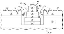
도 1은 본 발명의 실시예에 따른 디바이스(20)를 도시한다. 패키지형 디바이스(20)는 캐비티(21)를 갖는 열 확산기(22)를 포함한다. 도시된 실시예에서, 열 확산기(22)는 구리로 형성된다. 구리로 형성될 경우에, 열 확산기(22)는 크롬-실버(chromium-silver), 니켈-골드(nickel-gold), 등과 같은 다른 금속으로 도금될 수 있다. 다른 실시예에서, 열 확산기(22)는 임의의 다른 열 도전재로 형성될 수 있다. 패키지 기판(24)은 열 확산기(22)에 부착된다. 패키지 기판(24)은 또한 일반적으로 캐비티(21)의 개구에 대응하는 개구를 갖는다. 기판(24)의 상부는 하나 이상의 와이어 본드 핑거(30; wire bond fingers)와 하나 이상의 솔더 볼 패드(32; solder ball pads)를 포함한다. 본 발명의 일실시예에서, 패드(32)는 도전재로 형성되고 PCB에 디바이스(20)를 기계적 및 전기적으로 접속하는데 사용될 수 있다. 또한, 패드(32)는 개별적인 디바이스들을 실장하는데 사용될 수 있거나, 시험을 위해 테스트 프로브를 수용하는데 사용될 수 있거나, 또는 도전 접속부(예를 들어, 솔더 볼)를 수용하는데 사용될 수 있다. 도시된 실시예에서는, 와이어 본드 패드(30)는 상기 다이를 상기 패키지 기판에 전기 접속하는데 사용된다. 그러나, 다른 실시예에서는, 상기 다이를 상기 기판에 전기 접속하기 위해 다른 기술이 사용될 수 있다. 또한, 기판(24)은 상기 와이어 본드 패드(30)를 상기 솔더 볼 패드(32)에 접속하는 트레이스(trace)(도시되지 않음)와 같은 전기 도전체를 포함한다. 전기 회로를 갖는 반도체 다이(28)는 캐비티(21) 내에 정렬되고 다이 부착 물질(26)을 사용하여 열 확산기(22)에 부착된다. 선택적으로, 다이(28)는 다이 부착 테이프를 사용하여 열 확산기(22)에 부착될 수 있다.1 shows a
도 2는 제 2 다이(36)가 다이 부착 물질(34)을 사용하여 상기 다이(28)의 상부면에 정렬 및 부착되어 있는 패키지형 디바이스(20)의 일실시예를 도시한다. 일반적으로, 다이(36)는 자신이 부착되는 상기 다이(28)의 표면적보다 작은 표면적을 가지게 된다.2 shows one embodiment of a packaged
도 3은 제 2 열 확산기(40)가 상기 다이(36)의 상부면에 부착되어 있는 패키지형 디바이스(20)의 일실시예를 도시한다. 열 확산기(40)는 다이 부착 물질(38)을 사용하여 다이(36)의 상부면에 부착된다. 다이 부착 물질(38)은 예를 들어, 에폭시형 또는 테이프형 다이 부착 물질일 수 있다. 다른 실시예에서, 열 확산기(40)는 다이(36)상의 적당한 크기의 금속 패드(도시되지 않음)에 열 확산기(40)를 납땜함으로써 다이(36)에 부착될 수 있다. 열 확산기(40)는 웨이퍼가 개별 다이로 단일화되기 전에 또는 후에 상기 금속 패드에 납땜될 수 있다.3 shows one embodiment of a packaged
일실시예에서, 열 확산기(40)는 구리로 형성된다. 구리로 형성될 경우에, 열 확산기(40)는 크롬-실버, 니켈-골드, 등과 같은 다른 금속으로 도금될 수 있다. 다른 실시예에서, 열 확산기(40)는 예를 들어, 알루미늄 또는 금과 같은 다른 열 도 전재를 사용하여 형성될 수 있고, 스탬핑, 주조, 에칭 또는 기계가공에 의해 성형될 수 있다. 또한, 도시된 실시예에서, 열 확산기(40)는 참조번호 41로 지시된 테이퍼형 또는 계단형의 형상부 또는 융기부를 가지도록 형성되고, 열 확산기(40)의 하부면의 표면적은 열 확산기(40)의 상부면의 표면적보다 크다. 또한, 열 확산기(40)는 위에서 아래로 보았을 때 원통형 또는 직사각형일 수 있다. 열 확산기(40)에 원통 형상이 사용되면, 열 확산기(40)는 편평한 표면들이 서로 접속되는 두개의 원통으로서 가시화될 수 있고, 이 경우에 하나의 원통은 다른 원통보다 작은 직경을 갖는다. 열 확산기(40)에 직사각 형상이 사용되면, 연결되거나 인접하는 두개의 박스로서 가시화될 수 있고, 이 경우에 하나의 박스는 다른 박스와는 다른 체적을 갖는다. 다른 실시예에서는, 열 확산기(40)는 상이한 형상을 가질 수 있으며, 다수의 부품으로 형성될 수 있다.In one embodiment, the
도 4는 다이(28, 36)가 와이어 본드(44, 46)를 통해 본드 핑거(30)에 전기접속되어 있는 디바이스(20)의 일실시예를 도시한다. 본 발명의 선택적인 실시예는 임의의 개수의 와이어 본드(44, 46) 및 본드 핑거(30)를 사용할 수 있다. 또한, 선택안으로서 도 4에 도시된 와이어 본드(48)는 열 확산기(40)를 다이(36)상의 위치에 전기적으로 결합시킨다. 예를 들어, 와이어 본드(48)는 열 확산기(40)를 다이(36)에 전기적으로 접지시키는데 사용될 수 있다. 열 확산기(40)의 형상부(41)는 선택적인 와이어 본드를 용이하게 부착할 수 있는 위치로서 기능한다.4 shows one embodiment of a
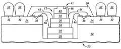
도 5는 캡슐화 물질(50; encapsulating material)이 적층 다이(36, 28), 열 확산기(40) 및 와이어 본드(44, 46, 및 48)의 위로 증착되어 있는 디바이스(20)의 일실시예를 도시한다. 캡슐화 물질(50)은 예를 들어, 성형된 플라스틱(molded plastic) 또는 증착된 액적 물질(liquid deposited glob material)과 같이 집적 회로에 적합한 임의의 형태의 물질일 수 있다는 점에 유의해야 한다. 또한, 캡슐화 물질(50)의 상부면은 열 확산기(40)의 상부면과 같은 높이로 형성되며, 열 확산기(40)의 상부면을 덮지 않는다는 점에 유의해야 한다. 또한, 상기 형상부(41)는 열 확산기(40)를 다이(36)의 상부에 고정하도록 기능하며, 디바이스(20)의 반복된 열 순환작동 이후에 열 확산기(40)가 캡슐화 물질(50)로부터 밀리는 것을 방지한다. 또한, 도시된 실시예에서, 캡슐화 물질(50)은 실질적으로 캐비티(21) 전체를 채운다.5 illustrates one embodiment of a
도 6은 복수의 솔더 볼(52)이 복수의 솔더 패드(32)상에 형성되어 있는 디바이스(20)의 일실시예를 도시한다. 솔더 볼(52)은 솔더 볼(52)을 증착하는 종래의 기술들 중 한가지 기술을 사용하여 형성된다.6 illustrates one embodiment of a
도 7은 디바이스(20)가 PCB(54)에 접속되어 있는 디바이스(20)의 일실시예를 도시한다. 도시된 실시예에서, 디바이스(20)를 PCB(54)에 부착하기 위해, 디바이스(20)가 회전 즉, 뒤집힌다는 점에 유의해야 한다. 그러나, 선택적인 실시예에서, 디바이스(20)는 그 형성 도중에 임의의 방식으로 배향될 수 있다. PCB(54)는 솔더 패드(32)의 위치에 대응하는 복수의 본드 패드(60)를 포함한다. 솔더 볼(52)은 가열 및 재유동되어 패드(60)에 대한 전기 접속부를 제공하고, 상기 패드(60)는 거기에 적용된 스크린 인쇄된 솔더 페이스트 등을 가질 수 있다. 또한, 솔더 접속부(56)는 열 확산기(40)와 PCB(54)상의 대응 패드(60) 사이에 형성된다.7 illustrates one embodiment of a
열 확산기(40)는 디바이스(20)의 제 2 열 소산 통로를 제공한다. 디바이스(20)의 작동 중에, 열 확산기(40)를 통해 적어도 다이(36)의 일부분으로부터 열이 소산된다. 다이(36)에 의해 발생된 열을 소산시키기 위한 다이(28)에 대한 필요성은 감소되며, 그에 따라 적층된 다이 반도체 디바이스가 보다 큰 열 소산을 가지도록 한다.The
기판(24) 내부의 트레이스 및 비아(via)(도시되지 않음)는 기판(24)의 다양한 부분들을 선택적으로 상호접속하는데 사용된다는 점에 유의해야 한다. 또한, 다이 부착 물질(26, 34, 및 38)은 예를 들어, 접착 테이프 또는 비-고형(non-solid) 접착제(예를 들어, 아교, 에폭시)와 같은 임의의 형태의 적절한 물질일 수 있다는 점에 유의해야 한다. 다이(28, 36)는 임의의 형태의 집적 회로, 반도체 디바이스, 또는 다른 형태의 전기적으로 능동인 기판일 수 있다. 본 발명의 선택적인 실시예는 패키지형 반도체 디바이스(20) 내부에 패키징된 임의의 개수의 다이(28, 36)를 가질 수 있다. 예를 들어, 선택적인 실시예는 패키지 디바이스(20) 내에 3개의 다이를 패키징할 수 있다. 다이(28, 36)의 사이즈 및 종횡비는 변경될 수 있다는 점에 유의해야 한다. 다이(28, 36)는 상기에 도시된 실시예에서는 열 확산기(22)의 캐비티(21) 내부에 위치된다는 점에 유의해야 한다. 그러나, 다른 실시예에서는, 다이(28) 및 다이(36)는 캐비티(21)를 가지지 않는 열 확산기상에 위치될 수 있다. 또한, 열 확산기(22)는 열 소산이 개선되도록 표면적을 증가시키기 위해 캐비티(21)의 반대쪽 측면이 패턴처리될 수 있다.It should be noted that traces and vias (not shown) inside the
전술한 설명에서, 본 발명은 특정 실시예를 참조로 기술되었다. 그러나, 당 업자라면, 하기의 청구범위에 기재된 바와 같은 본 발명의 범위로부터 일탈함이 없이 다양한 변형 및 변경이 취해질 수 있다는 것을 이해할 것이다. 예를 들어, 임의의 적절한 다이 부착 공정, 와이어 본드 공정, 솔더 볼 형성 공정 및 테이프 공정은 본 기술분야에 공지되어 있는 패키지 디바이스(20)의 형성에 사용될 수 있다. 결과적으로, 명세서 및 도면은 제한적인 것이라기 보다는 예시적인 것으로 고려되어야 하고, 상기 모든 변형은 본 발명의 범위 내에 포함되어야 한다. 이점, 다른 장점, 및 문제점에 대한 해법은 특정 실시예에 관해서 설명되었다. 그러나, 상기 이점, 장점, 및 문제점에 대한 해법과, 임의의 이점, 장점, 또는 발생하거나 주장되는 해법을 야기할 수 있는 임의의 요소(들)는 임의의 특허청구범위의 중요하거나, 필요하거나, 본질적인 양태 또는 요소로서 이해되지는 않는다.In the foregoing description, the invention has been described with reference to specific embodiments. However, one of ordinary skill in the art appreciates that various modifications and changes can be made without departing from the scope of the present invention as set forth in the claims below. For example, any suitable die attach process, wire bond process, solder ball forming process, and tape process can be used to form the
본 발명에 의하면, 상부 다이에 열 확산기를 부착함으로써 열 소산을 개선한 적층 다이용 패키지형 반도체 디바이스가 제공되며, 상기 상부 다이에 부착된 열 확산기는 하부 다이를 지지하는데 사용되는 열 확산기를 보조한다. 상기 하부 열 확산기는 상기 디바이스의 높이를 감소시키기 위해 상기 적층 다이를 지지하는 캐비티를 구비한다. 상기 패키지형 디바이스가 인쇄 회로 기판(PCB)에 부착되면, 상기 상부 다이에 부착된 열 확산기는 상기 PCB와 접촉하고 상기 상부 다이의 작동에 의해 발생된 열을 감소시키는 직접적인 열 통로를 제공한다.
According to the present invention, there is provided a packaged semiconductor device for a stacked die that improves heat dissipation by attaching a heat spreader to an upper die, wherein the heat spreader attached to the upper die assists the heat spreader used to support the lower die. . The bottom heat spreader has a cavity supporting the stacked die to reduce the height of the device. When the packaged device is attached to a printed circuit board (PCB), the heat spreader attached to the upper die provides a direct heat path that contacts the PCB and reduces heat generated by the operation of the upper die.
Claims (3)
Translated fromKoreanApplications Claiming Priority (2)
| Application Number | Priority Date | Filing Date | Title |
|---|---|---|---|
| US10/072,167US6858932B2 (en) | 2002-02-07 | 2002-02-07 | Packaged semiconductor device and method of formation |
| US10/072,167 | 2002-02-07 |
Publications (2)
| Publication Number | Publication Date |
|---|---|
| KR20030067542A KR20030067542A (en) | 2003-08-14 |
| KR100995478B1true KR100995478B1 (en) | 2010-11-22 |
Family
ID=27610553
Family Applications (1)
| Application Number | Title | Priority Date | Filing Date |
|---|---|---|---|
| KR1020030007424AExpired - Fee RelatedKR100995478B1 (en) | 2002-02-07 | 2003-02-06 | Packaged semiconductor device and method of forming the same |
Country Status (5)
| Country | Link |
|---|---|
| US (1) | US6858932B2 (en) |
| EP (1) | EP1335426A3 (en) |
| JP (1) | JP4653383B2 (en) |
| KR (1) | KR100995478B1 (en) |
| CN (2) | CN101150098B (en) |
Families Citing this family (13)
| Publication number | Priority date | Publication date | Assignee | Title |
|---|---|---|---|---|
| US6853070B2 (en)* | 2001-02-15 | 2005-02-08 | Broadcom Corporation | Die-down ball grid array package with die-attached heat spreader and method for making the same |
| US6794748B1 (en)* | 2003-04-22 | 2004-09-21 | Intel Corporation | Substrate-less microelectronic package |
| US7190068B2 (en)* | 2004-06-25 | 2007-03-13 | Intel Corporation | Bottom heat spreader |
| US7071556B2 (en)* | 2004-09-10 | 2006-07-04 | Jinghui Mu | Tape ball grid array package with electromagnetic interference protection and method for fabricating the package |
| US7786591B2 (en) | 2004-09-29 | 2010-08-31 | Broadcom Corporation | Die down ball grid array package |
| KR100700936B1 (en)* | 2006-01-25 | 2007-03-28 | 삼성전자주식회사 | Cooling unit and memory module having same |
| US9713258B2 (en)* | 2006-04-27 | 2017-07-18 | International Business Machines Corporation | Integrated circuit chip packaging |
| US20090039524A1 (en)* | 2007-08-08 | 2009-02-12 | Texas Instruments Incorporated | Methods and apparatus to support an overhanging region of a stacked die |
| US8472190B2 (en)* | 2010-09-24 | 2013-06-25 | Ati Technologies Ulc | Stacked semiconductor chip device with thermal management |
| TWI446495B (en)* | 2011-01-19 | 2014-07-21 | Subtron Technology Co Ltd | Package carrier board and manufacturing method thereof |
| US9070657B2 (en) | 2013-10-08 | 2015-06-30 | Freescale Semiconductor, Inc. | Heat conductive substrate for integrated circuit package |
| KR20170001238A (en)* | 2015-06-26 | 2017-01-04 | 에스케이하이닉스 주식회사 | Semiconductor package including step type substrate |
| US10741534B2 (en)* | 2018-09-28 | 2020-08-11 | Intel Corporation | Multi-die microelectronic device with integral heat spreader |
Citations (4)
| Publication number | Priority date | Publication date | Assignee | Title |
|---|---|---|---|---|
| JP2000332160A (en)* | 1999-05-24 | 2000-11-30 | Sumitomo Metal Electronics Devices Inc | Cavity down type semiconductor package |
| US6184580B1 (en)* | 1999-09-10 | 2001-02-06 | Siliconware Precision Industries Co., Ltd. | Ball grid array package with conductive leads |
| JP2001068512A (en)* | 1999-08-27 | 2001-03-16 | Hitachi Cable Ltd | TAB tape and BGA package with stiffener |
| JP2001267469A (en) | 2000-03-16 | 2001-09-28 | Denso Corp | Resin sealing semiconductor device |
Family Cites Families (26)
| Publication number | Priority date | Publication date | Assignee | Title |
|---|---|---|---|---|
| JPS61232651A (en)* | 1985-04-09 | 1986-10-16 | Seiko Epson Corp | Semiconductor mounting method |
| JP2660732B2 (en)* | 1989-01-09 | 1997-10-08 | 株式会社日立製作所 | Semiconductor device |
| JPH0458539A (en)* | 1990-06-27 | 1992-02-25 | Mitsubishi Electric Corp | Hybrid integrated circuit device |
| US5216278A (en)* | 1990-12-04 | 1993-06-01 | Motorola, Inc. | Semiconductor device having a pad array carrier package |
| US5468994A (en) | 1992-12-10 | 1995-11-21 | Hewlett-Packard Company | High pin count package for semiconductor device |
| JP2591499B2 (en)* | 1994-10-21 | 1997-03-19 | 日本電気株式会社 | Semiconductor device |
| JP2636777B2 (en) | 1995-02-14 | 1997-07-30 | 日本電気株式会社 | Semiconductor module for microprocessor |
| TW373308B (en)* | 1995-02-24 | 1999-11-01 | Agere Systems Inc | Thin packaging of multi-chip modules with enhanced thermal/power management |
| JPH0917919A (en) | 1995-06-29 | 1997-01-17 | Fujitsu Ltd | Semiconductor device |
| US5844168A (en) | 1995-08-01 | 1998-12-01 | Minnesota Mining And Manufacturing Company | Multi-layer interconnect sutructure for ball grid arrays |
| JPH0992748A (en)* | 1995-09-21 | 1997-04-04 | Mitsubishi Materials Corp | Package for semiconductor element |
| KR19990067623A (en)* | 1995-11-28 | 1999-08-25 | 가나이 쓰도무 | Semiconductor device, manufacturing method and mounting board |
| US5843808A (en) | 1996-01-11 | 1998-12-01 | Asat, Limited | Structure and method for automated assembly of a tab grid array package |
| US5696031A (en) | 1996-11-20 | 1997-12-09 | Micron Technology, Inc. | Device and method for stacking wire-bonded integrated circuit dice on flip-chip bonded integrated circuit dice |
| KR100214549B1 (en)* | 1996-12-30 | 1999-08-02 | 구본준 | Bottom Lead Semiconductor Package |
| US6008536A (en)* | 1997-06-23 | 1999-12-28 | Lsi Logic Corporation | Grid array device package including advanced heat transfer mechanisms |
| US5919329A (en) | 1997-10-14 | 1999-07-06 | Gore Enterprise Holdings, Inc. | Method for assembling an integrated circuit chip package having at least one semiconductor device |
| JPH11219984A (en) | 1997-11-06 | 1999-08-10 | Sharp Corp | Semiconductor device package, method of manufacturing the same, and circuit board therefor |
| JP3610769B2 (en)* | 1998-03-25 | 2005-01-19 | イビデン株式会社 | Multi-layer electronic component mounting board |
| JP2000077563A (en)* | 1998-08-31 | 2000-03-14 | Sharp Corp | Semiconductor device and method of manufacturing the same |
| JP2000174180A (en)* | 1998-12-02 | 2000-06-23 | Shibafu Engineering Kk | Semiconductor device |
| JP3512657B2 (en) | 1998-12-22 | 2004-03-31 | シャープ株式会社 | Semiconductor device |
| JP3344362B2 (en)* | 1999-05-07 | 2002-11-11 | 日本電気株式会社 | Film carrier type semiconductor device |
| TW429494B (en)* | 1999-11-08 | 2001-04-11 | Siliconware Precision Industries Co Ltd | Quad flat non-leaded package |
| JP2001267476A (en)* | 2000-03-17 | 2001-09-28 | Aronshiya:Kk | Method for manufacturing heat spreader for semiconductor package |
| TW466723B (en)* | 2000-12-01 | 2001-12-01 | Siliconware Precision Industries Co Ltd | Super thin package having high heat-dissipation property |
- 2002
- 2002-02-07USUS10/072,167patent/US6858932B2/ennot_activeExpired - Lifetime
- 2003
- 2003-01-30CNCN2006101075528Apatent/CN101150098B/ennot_activeExpired - Lifetime
- 2003-01-30CNCNB031023126Apatent/CN1319138C/ennot_activeExpired - Lifetime
- 2003-02-04EPEP03002380Apatent/EP1335426A3/ennot_activeWithdrawn
- 2003-02-06KRKR1020030007424Apatent/KR100995478B1/ennot_activeExpired - Fee Related
- 2003-02-07JPJP2003030887Apatent/JP4653383B2/ennot_activeExpired - Fee Related
Patent Citations (4)
| Publication number | Priority date | Publication date | Assignee | Title |
|---|---|---|---|---|
| JP2000332160A (en)* | 1999-05-24 | 2000-11-30 | Sumitomo Metal Electronics Devices Inc | Cavity down type semiconductor package |
| JP2001068512A (en)* | 1999-08-27 | 2001-03-16 | Hitachi Cable Ltd | TAB tape and BGA package with stiffener |
| US6184580B1 (en)* | 1999-09-10 | 2001-02-06 | Siliconware Precision Industries Co., Ltd. | Ball grid array package with conductive leads |
| JP2001267469A (en) | 2000-03-16 | 2001-09-28 | Denso Corp | Resin sealing semiconductor device |
Also Published As
| Publication number | Publication date |
|---|---|
| KR20030067542A (en) | 2003-08-14 |
| CN1319138C (en) | 2007-05-30 |
| CN101150098B (en) | 2011-11-23 |
| EP1335426A2 (en) | 2003-08-13 |
| CN101150098A (en) | 2008-03-26 |
| CN1437233A (en) | 2003-08-20 |
| JP2003243565A (en) | 2003-08-29 |
| JP4653383B2 (en) | 2011-03-16 |
| US6858932B2 (en) | 2005-02-22 |
| EP1335426A3 (en) | 2008-07-30 |
| US20030148554A1 (en) | 2003-08-07 |
Similar Documents
| Publication | Publication Date | Title |
|---|---|---|
| KR100260997B1 (en) | Semiconductor package | |
| US7960827B1 (en) | Thermal via heat spreader package and method | |
| US9947641B2 (en) | Wire bond support structure and microelectronic package including wire bonds therefrom | |
| USRE42653E1 (en) | Semiconductor package with heat dissipating structure | |
| US5991156A (en) | Ball grid array integrated circuit package with high thermal conductivity | |
| US5285352A (en) | Pad array semiconductor device with thermal conductor and process for making the same | |
| US7928590B2 (en) | Integrated circuit package with a heat dissipation device | |
| US5834839A (en) | Preserving clearance between encapsulant and PCB for cavity-down single-tier package assembly | |
| KR20050064144A (en) | Semiconductor module having semiconductor chip package which is vertically mounted on module board | |
| KR100698526B1 (en) | A wiring board having a heat dissipation layer and a semiconductor package using the same | |
| KR20050077866A (en) | Semiconductor package with heat-dissipating structure and method for fabricating the same | |
| US6501164B1 (en) | Multi-chip semiconductor package with heat dissipating structure | |
| KR100995478B1 (en) | Packaged semiconductor device and method of forming the same | |
| US6559537B1 (en) | Ball grid array packages with thermally conductive containers | |
| US20020189853A1 (en) | BGA substrate with direct heat dissipating structure | |
| US6750397B2 (en) | Thermally enhanced semiconductor build-up package | |
| US8031484B2 (en) | IC packages with internal heat dissipation structures | |
| KR20020043395A (en) | Semiconductor package | |
| KR101089647B1 (en) | Single layer package substrate and manufacturing method thereof | |
| EP0676806B1 (en) | Ball grid array intergrated circuit package with high thermal conductivity | |
| KR20080067891A (en) | Multi-chip package | |
| KR100674411B1 (en) | Semiconductor Package Using Core Ball and Manufacturing Method Thereof | |
| KR100708050B1 (en) | Semiconductor Package | |
| KR20000011420U (en) | Stacked Semiconductor Packages | |
| KR20050104204A (en) | Stack package |
Legal Events
| Date | Code | Title | Description |
|---|---|---|---|
| PA0109 | Patent application | St.27 status event code:A-0-1-A10-A12-nap-PA0109 | |
| PG1501 | Laying open of application | St.27 status event code:A-1-1-Q10-Q12-nap-PG1501 | |
| R17-X000 | Change to representative recorded | St.27 status event code:A-3-3-R10-R17-oth-X000 | |
| N231 | Notification of change of applicant | ||
| PN2301 | Change of applicant | St.27 status event code:A-3-3-R10-R13-asn-PN2301 St.27 status event code:A-3-3-R10-R11-asn-PN2301 | |
| R17-X000 | Change to representative recorded | St.27 status event code:A-3-3-R10-R17-oth-X000 | |
| A201 | Request for examination | ||
| PA0201 | Request for examination | St.27 status event code:A-1-2-D10-D11-exm-PA0201 | |
| D13-X000 | Search requested | St.27 status event code:A-1-2-D10-D13-srh-X000 | |
| D14-X000 | Search report completed | St.27 status event code:A-1-2-D10-D14-srh-X000 | |
| E902 | Notification of reason for refusal | ||
| PE0902 | Notice of grounds for rejection | St.27 status event code:A-1-2-D10-D21-exm-PE0902 | |
| E13-X000 | Pre-grant limitation requested | St.27 status event code:A-2-3-E10-E13-lim-X000 | |
| P11-X000 | Amendment of application requested | St.27 status event code:A-2-2-P10-P11-nap-X000 | |
| P13-X000 | Application amended | St.27 status event code:A-2-2-P10-P13-nap-X000 | |
| R17-X000 | Change to representative recorded | St.27 status event code:A-3-3-R10-R17-oth-X000 | |
| E90F | Notification of reason for final refusal | ||
| PE0902 | Notice of grounds for rejection | St.27 status event code:A-1-2-D10-D21-exm-PE0902 | |
| P11-X000 | Amendment of application requested | St.27 status event code:A-2-2-P10-P11-nap-X000 | |
| P13-X000 | Application amended | St.27 status event code:A-2-2-P10-P13-nap-X000 | |
| R18-X000 | Changes to party contact information recorded | St.27 status event code:A-3-3-R10-R18-oth-X000 | |
| R18-X000 | Changes to party contact information recorded | St.27 status event code:A-3-3-R10-R18-oth-X000 | |
| E701 | Decision to grant or registration of patent right | ||
| PE0701 | Decision of registration | St.27 status event code:A-1-2-D10-D22-exm-PE0701 | |
| R18-X000 | Changes to party contact information recorded | St.27 status event code:A-3-3-R10-R18-oth-X000 | |
| GRNT | Written decision to grant | ||
| PR0701 | Registration of establishment | St.27 status event code:A-2-4-F10-F11-exm-PR0701 | |
| PR1002 | Payment of registration fee | St.27 status event code:A-2-2-U10-U11-oth-PR1002 Fee payment year number:1 | |
| PG1601 | Publication of registration | St.27 status event code:A-4-4-Q10-Q13-nap-PG1601 | |
| R18-X000 | Changes to party contact information recorded | St.27 status event code:A-5-5-R10-R18-oth-X000 | |
| FPAY | Annual fee payment | Payment date:20131025 Year of fee payment:4 | |
| PR1001 | Payment of annual fee | St.27 status event code:A-4-4-U10-U11-oth-PR1001 Fee payment year number:4 | |
| FPAY | Annual fee payment | Payment date:20141028 Year of fee payment:5 | |
| PR1001 | Payment of annual fee | St.27 status event code:A-4-4-U10-U11-oth-PR1001 Fee payment year number:5 | |
| FPAY | Annual fee payment | Payment date:20151027 Year of fee payment:6 | |
| PR1001 | Payment of annual fee | St.27 status event code:A-4-4-U10-U11-oth-PR1001 Fee payment year number:6 | |
| FPAY | Annual fee payment | Payment date:20161027 Year of fee payment:7 | |
| PR1001 | Payment of annual fee | St.27 status event code:A-4-4-U10-U11-oth-PR1001 Fee payment year number:7 | |
| PN2301 | Change of applicant | St.27 status event code:A-5-5-R10-R13-asn-PN2301 St.27 status event code:A-5-5-R10-R11-asn-PN2301 | |
| LAPS | Lapse due to unpaid annual fee | ||
| PC1903 | Unpaid annual fee | St.27 status event code:A-4-4-U10-U13-oth-PC1903 Not in force date:20171116 Payment event data comment text:Termination Category : DEFAULT_OF_REGISTRATION_FEE | |
| PC1903 | Unpaid annual fee | St.27 status event code:N-4-6-H10-H13-oth-PC1903 Ip right cessation event data comment text:Termination Category : DEFAULT_OF_REGISTRATION_FEE Not in force date:20171116 |