KR100995146B1 - System and method for controlling device access to memory providing improved memory access security - Google Patents
System and method for controlling device access to memory providing improved memory access securityDownload PDFInfo
- Publication number
- KR100995146B1 KR100995146B1KR1020047008690AKR20047008690AKR100995146B1KR 100995146 B1KR100995146 B1KR 100995146B1KR 1020047008690 AKR1020047008690 AKR 1020047008690AKR 20047008690 AKR20047008690 AKR 20047008690AKR 100995146 B1KR100995146 B1KR 100995146B1
- Authority
- KR
- South Korea
- Prior art keywords
- memory
- page
- security
- security attribute
- access
- Prior art date
- Legal status (The legal status is an assumption and is not a legal conclusion. Google has not performed a legal analysis and makes no representation as to the accuracy of the status listed.)
- Expired - Fee Related
Links
Images


Classifications
- G—PHYSICS
- G06—COMPUTING OR CALCULATING; COUNTING
- G06F—ELECTRIC DIGITAL DATA PROCESSING
- G06F12/00—Accessing, addressing or allocating within memory systems or architectures
- G06F12/14—Protection against unauthorised use of memory or access to memory
- G—PHYSICS
- G06—COMPUTING OR CALCULATING; COUNTING
- G06F—ELECTRIC DIGITAL DATA PROCESSING
- G06F12/00—Accessing, addressing or allocating within memory systems or architectures
- G06F12/14—Protection against unauthorised use of memory or access to memory
- G06F12/1416—Protection against unauthorised use of memory or access to memory by checking the object accessibility, e.g. type of access defined by the memory independently of subject rights
- G06F12/1425—Protection against unauthorised use of memory or access to memory by checking the object accessibility, e.g. type of access defined by the memory independently of subject rights the protection being physical, e.g. cell, word, block
- G06F12/1441—Protection against unauthorised use of memory or access to memory by checking the object accessibility, e.g. type of access defined by the memory independently of subject rights the protection being physical, e.g. cell, word, block for a range
- G—PHYSICS
- G06—COMPUTING OR CALCULATING; COUNTING
- G06F—ELECTRIC DIGITAL DATA PROCESSING
- G06F12/00—Accessing, addressing or allocating within memory systems or architectures
- G06F12/14—Protection against unauthorised use of memory or access to memory
- G06F12/1458—Protection against unauthorised use of memory or access to memory by checking the subject access rights
- G06F12/1491—Protection against unauthorised use of memory or access to memory by checking the subject access rights in a hierarchical protection system, e.g. privilege levels, memory rings
Landscapes
- Engineering & Computer Science (AREA)
- Theoretical Computer Science (AREA)
- Computer Security & Cryptography (AREA)
- Physics & Mathematics (AREA)
- General Engineering & Computer Science (AREA)
- General Physics & Mathematics (AREA)
- Storage Device Security (AREA)
- Memory System Of A Hierarchy Structure (AREA)
Abstract
Translated fromKoreanDescription
Translated fromKorean본 발명은 일반적으로 메모리 관리 시스템들 및 방법들에 관한 것으로, 특히 메모리내에 저장된 데이타를 보호하는 메모리 관리 시스템들 및 방법들에 관한 것이다.The present invention relates generally to memory management systems and methods, and more particularly to memory management systems and methods for protecting data stored in memory.
통상적인 컴퓨터 시스템은 상대적으로 낮은 비용으로 상대적으로 높은 레벨의 성능을 획득하기 위한 메모리 계층(memory hierarchy)을 포함한다. 다수의 상이한 소프트웨어 프로그램들의 명령들은 통상 상대적으로 저장 용량이 크나 저장 속도가 느린 비휘발성 저장 유닛(예를 들어, 디스크 구동 유닛)에 저장된다. 유저가 실행을 위해 이들 프로그램들 중 하나를 선택하면, 선택된 프로그램의 명령들이 메인 메모리 유닛(예를 들어, 랜덤 엑세스 메모리(RAM))내에 카피되고, 중앙 처리 유닛(CPU)은 상기 메인 메모리 유닛으로부터 상기 선택된 프로그램의 명령들을 획득한다. 널리 공지된 가상 메모리 관리 기술은 상기 CPU가 임의의 소정의 시간에 상기 메인 메모리내에 데이타 구조들의 일부분을 저장함으로써 상기 메인 메모리의 크기보다 크기가 더 큰 데이타 구조들에 엑세스하게 한다. 상기 데이타 구조들의 나머지들은 상대적으로 저장 용량이 크나 저장 속도가 느린 비휘발성 저장 유닛내에 저장되고, 필요할 시에만 상기 메인 메모리 유닛내에 카피된다.Conventional computer systems include a memory hierarchy for obtaining relatively high levels of performance at relatively low cost. Instructions of many different software programs are typically stored in a nonvolatile storage unit (e.g., a disk drive unit) having a relatively large storage capacity but a slow storage speed. When the user selects one of these programs for execution, the instructions of the selected program are copied into the main memory unit (e.g., random access memory (RAM)), and the central processing unit (CPU) from the main memory unit Obtain the commands of the selected program. Well-known virtual memory management techniques allow the CPU to access portions of data structures that are larger than the size of the main memory by storing portions of the data structures in the main memory at any given time. The rest of the data structures are stored in a nonvolatile storage unit having a relatively large storage capacity but a slow storage speed, and are copied into the main memory unit only when necessary.
가상 메모리는 통상 상기 CPU의 어드레스 공간을 페이지 프레임 또는 "페이지들"이라고 칭하는 다수의 블럭들로 분할함으로써 구현된다. 상기 페이지들의 일부분에 대응하는 데이타만이 임의의 소정의 시간에 상기 메인 메모리 유닛내에 저장된다. 상기 CPU가 소정의 페이지내의 어드레스를 발생시키고 그 페이지의 카피(copy)가 상기 메인 메모리 유닛내에 위치되지 않으면, 데이타의 요구된 페이지가 상기 저장 용량이 크나 저장 속도가 느린 비휘발성 저장 유닛으로부터 상기 메인 메모리 유닛내로 카피된다. 이 과정에서, 데이타의 또 다른 페이지가 상기 메인 메모리 유닛으로부터 상기 비-휘발성 저장 유닛으로 카피되어, 상기 요구된 페이지를 위한 공간(room)을 만들 수 있다.Virtual memory is typically implemented by dividing the address space of the CPU into a number of blocks called page frames or " pages. &Quot; Only data corresponding to a portion of the pages is stored in the main memory unit at any given time. If the CPU generates an address in a given page and a copy of that page is not located in the main memory unit, the requested page of data is stored in the main memory from a nonvolatile storage unit having a large storage capacity but a slow storage speed. Copied into the memory unit. In this process, another page of data can be copied from the main memory unit to the non-volatile storage unit to make room for the requested page.
널리 보급된 80 ×86(×86) 프로세서 아키텍쳐는 보호 가상 어드레스 모드(즉, 보호 모드)를 지원하기 위한 특수 하드웨어 요소들을 포함한다. 이제, 도 1 내지 도 3은 ×86 프로세서가 가상 메모리와 메모리 보호 특징들 양자를 어떻게 구현하는 지를 설명한다. 도 1은 상기 ×86 프로세서 아키텍쳐의 널리 공지된 선형-대-물리적(linear to physical) 어드레스 변환 매카니즘(100)의 다이어그램이다. 어드레스 변환 매카니즘(100)이 ×86 프로세서내에 내장되고, 상기 ×86 프로세서내에 생성된 선형 어드레스(102)와, 페이지 테이블 디렉토리(즉, 페이지 디렉토리)(104)와, 페이지 테이블(106)을 포함하는 다수의 페이지 테이블들과, 페이지 프레임(108)을 포함하는 다수의 페이지 프레임들과, 그리고 제어 레지스터(CR3)(110)를 포함한다. 상기 페이지 디렉토리(104) 및 상기 다수의 페이지 테이블들은 오퍼레이팅 시스템 소프트웨어(즉, 오퍼레이팅 시스템)에 의해 생성 및 유지된 메모리 데이타 구조들을 페이징한다. 상기 페이지 디렉토리(104)는 항상 상기 메모리(예를 들어, 상기 메인 메모리 유닛)내에 위치된다. 간단히 하기 위해, 상기 페이지 테이블(106) 및 페이지 프레임(108)도 또한 상기 메모리내에 상주하는 것으로 가정한다.The widespread 80 x 86 (x86) processor architecture includes special hardware elements to support protected virtual address mode (ie, protected mode). 1-3 illustrate how a x86 processor implements both virtual memory and memory protection features. 1 is a diagram of a well-known linear-to-physical
도 1에 도시된 바와같이, 선형 어드레스(102)는 3개의 부분으로 분할되어 선형-대-물리적 어드레스 변환을 성취한다. 상기 CR3(110)의 최고 순위 비트들이 페이지 디렉토리 베이스 레지스터를 저장하기 위해 사용된다. 상기 페이지 디렉토리 베이스 레지스터는 페이지 디렉토리(104)를 포함한 메모리 페이지의 기준(base) 어드레스이다. 상기 페이지 디렉토리(104)는 페이지 디렉토리 엔트리(112)를 포함하는 다수의 페이지 디렉토리 엔트리들을 포함한다. 선형 어드레스(102)의 최고 순위 또는 최상위 비트들을 포함하는 상기 선형 어드레스(102)의 상위 "디렉토리 색인" 부분이 상기 페이지 디렉토리(104)내에서 색인으로서 사용된다. 상기 페이지 디렉토리 엔트리(112)는 상기 CR3(110)의 페이지 디렉토리 기준 어드레스와 상기 선형 어드레스(102)의 상위 "디렉토리 색인" 부분을 사용하여 페이지 디렉토리(104)내에서 부터 선택된다.As shown in FIG. 1, the linear address 102 is divided into three parts to achieve linear-to-physical address translation. The most significant bits of the
도 2는 상기 ×86 프로세서 아키텍쳐의 페이지 디렉토리 엔트리 포맷(200)의 다이어그램이다. 도 2에 도시된 바와같이, 소정의 페이지 디렉토리 엔트리의 최고 순위(즉, 최상위) 비트들은 페이지 테이블 기준 어드레스를 포함하며, 여기서 상기 페이지 테이블 기준 어드레스는 대응하는 페이지 테이블을 포함하는 메모리 페이지의 기준 어드레스이다. 상기 페이지 디렉토리 엔트리(112)의 상기 페이지 테이블 기준 어드레스는 대응하는 페이지 테이블(106)을 선택하기 위해 사용된다.2 is a diagram of the page directory entry format 200 of the x86 processor architecture. As shown in FIG. 2, the highest order (ie, most significant) bits of a given page directory entry include a page table reference address, where the page table reference address is a reference address of a memory page that includes a corresponding page table. to be. The page table reference address of the page directory entry 112 is used to select the corresponding page table 106.
도 1을 재차 고려해볼 때, 페이지 테이블(106)은 페이지 테이블 엔트리(114)를 포함하는 다수의 페이지 테이블 엔트리들을 포함한다. 상기 선형 어드레스(102)의 중간의 "테이블 색인" 부분이 상기 페이지 테이블(106)내에서 색인으로서 사용되며, 이에 의해 상기 페이지 테이블 엔트리(114)를 선택한다. 도 3은 상기 ×86 프로세서 아키텍쳐의 페이지 테이블 엔트리 포맷(300)의 다이어그램이다. 도 3에 도시된 바와같이, 소정의 페이지 테이블 엔트리의 최고 순위(즉, 최상위) 비트들은 페이지 프레임 기준 어드레스를 포함하며, 여기서 상기 페이지 프레임 기준 어드레스는 대응하는 페이지 프레임의 기준 어드레스이다.Referring back to FIG. 1, the page table 106 includes a number of page table entries including a page table entry 114. The middle “table index” portion of the linear address 102 is used as an index in the page table 106, thereby selecting the page table entry 114. 3 is a diagram of a page table entry format 300 of the x86 processor architecture. As shown in FIG. 3, the highest order (ie, most significant) bits of a given page table entry include a page frame reference address, where the page frame reference address is the reference address of the corresponding page frame.
도 1을 재차 고려해볼 때, 상기 페이지 테이블 엔트리(114)의 페이지 프레임 기준 어드레스는 대응하는 페이지 프레임(108)을 선택하기 위해 사용된다. 상기 페이지 프레임(108)은 다수의 메모리 위치들을 포함한다. 상기 선형 어드레스(102)의 하위 또는 "오프셋" 부분은 상기 페이지 프레임(108)내에서 색인으로서 사용된다. 이들 하위 또는 "오프셋" 부분과 상기 페이지 프레임(108)이 결합되면, 상기 페이지 테이블 엔트리(114)의 페이지 프레임 기준 어드레스와 상기 선형 어드레스(102)의 상기 오프셋 부분이 상기 선형 어드레스(102)에 대응하는 물리적 어드레스를 생성하고, 상기 페이지 프레임(108)내에서의 메모리 위치(116)를 나타낸다. 상기 메모리 위치(116)는 상기 선형-대-물리적 어드레스 변환으로부터 발생된 물리적 어드레스를 갖고있다.Referring back to FIG. 1, the page frame reference address of the page table entry 114 is used to select the
메모리 보호 특징들에 관하여, 도 2의 페이지 디렉토리 엔트리 포맷(200)과 도 3의 페이지 테이블 엔트리 포맷(300)은 유저/슈퍼바이저(U/S) 비트 및 판독/기록(R/W) 비트를 포함한다. 상기 U/S 및 R/W 비트들의 내용들이 오퍼레이팅 시스템에 의해 사용되어, 허가되지 않은 엑세스로 부터의 대응하는 페이지 프레임들(즉, 메모리 페이지들)을 보호한다. U/S=0 은 오퍼레이팅 시스템 메모리 페이지를 나타내는데 사용되고 상기 오퍼레이팅 시스템의 "슈퍼바이저" 레벨에 대응한다. 상기 오퍼레이팅 시스템의 슈퍼바이저 레벨은 상기 ×86 프로세서에 의해 실행되는 소프트웨어 프로그램들 및 루틴들의 현재의 특권 레벨 0(current privilege level: CPL0)에 대응한다. U/S>0(즉, U/S=1, 2, 3)은 유저 메모리 페이지를 나타내는데 사용되고 상기 오퍼레이팅 시스템의 "유저" 레벨에 대응한다.With regard to memory protection features, the page directory entry format 200 of FIG. 2 and the page table entry format 300 of FIG. 3 may include user / supervisor (U / S) bits and read / write (R / W) bits. Include. The contents of the U / S and R / W bits are used by the operating system to protect corresponding page frames (ie memory pages) from unauthorized access. U / S = 0 is used to represent an operating system memory page and corresponds to the “supervisor” level of the operating system. The supervisor level of the operating system corresponds to the current privilege level (CPL0) of software programs and routines executed by the x86 processor. U / S> 0 (ie U / S = 1, 2, 3) is used to represent user memory pages and corresponds to the " user " level of the operating system.
상기 R/W 비트는 대응하는 메모리 페이지에 허용된 엑세스들의 형식을 나타내는데 사용된다. R/W=0는 판독 엑세스만이 상기 대응하는 메모리 페이지에 허용된다는 것을 나타낸다(즉, 상기 대응하는 메모리 페이지가 "판독-전용(read-only)"임). R/W=1는 판독 및 기록 엑세스들 양자가 상기 대응하는 메모리 페이지에 허용된다는 것을 나타낸다(즉, 상기 대응하는 메모리 페이지가 "판독-기록(read-write)"임).The R / W bit is used to indicate the type of accesses allowed to the corresponding memory page. R / W = 0 indicates that only read access is allowed to the corresponding memory page (ie, the corresponding memory page is "read-only"). R / W = 1 indicates that both read and write accesses are allowed to the corresponding memory page (ie, the corresponding memory page is “read-write”).
도 1의 상기 선형-대-물리적 어드레스 변환 동안, 상기 페이지 프레임(108)에 대응하는 상기 페이지 디렉토리 엔트리(112) 및 상기 페이지 테이블 엔트리(114)의 상기 U/S 비트의 내용들은, 상기 페이지 프레임(108)으로의 엑세스가 허가되는 지를 결정하기 위해 논리적으로 AND화된다. 마찬가지로, 상기 페이지 디렉토리 엔트리(112) 및 상기 페이지 테이블 엔트리(114)의 상기 R/W 비트들의 내용들은 상기 페이지 프레임(108)으로의 엑세스가 허가되는 지를 결정하기 위해 논리적으로 AND화된다. 상기 U/S 및 R/W 비트들의 논리 조합이 상기 페이지 프레임(108)으로의 엑세스가 허가되는 것을 나타낸다면, 상기 메모리 위치(116)는 물리적 어드레스를 사용하여 엑세스된다. 한편, 상기 U/S 및 R/W 비트들의 논리 조합이 상기 페이지 프레임(108)으로의 엑세스가 허가되지 않는 것을 나타낸다면, 상기 메모리 위치(116)는 엑세스되지 않고, 보호 위반(fault) 표시 신호가 발신된다.During the linear-to-physical address translation of FIG. 1, the contents of the U / S bits of the page directory entry 112 and the page table entry 114 corresponding to the
아쉽게도, 상기 ×86 프로세서 아키텍쳐의 전술된 메모리 보호 매카니즘은 상기 메모리에 저장된 데이타를 보호하기에 충분치 않다. 예를 들어, 슈퍼바이저 레벨(예를 들어, 0의 CPL을 갖는)에서 실행된 임의의 소프트웨어 프로그램 또는 루틴은 상기 메모리의 임의의 부분에 엑세스할 수 있고, "판독-전용"(R/W=0)으로 표시되지 않은 상기 메모리의 임의의 부분을 변경(즉, 기록(writing))할 수 있다. 게다가, 슈퍼바이저 레벨에서의 실행에 의해, 소프트웨어 프로그램 또는 루틴이 상기 메모리의 임의의 부분의 속성(즉, 상기 U/S 및 R/W 비트들)을 변화시킬 수 있다. 따라서, 상기 소프트웨어 프로그램 또는 루틴이 "판독-전용"으로 표시된 상기 메모리의 임의의 부분을 "판독-기록"(R/W=1)으로 변화시키고 그래서, 상기 메모리의 상기 부분을 변경하도록 처리될 수 있다.Unfortunately, the aforementioned memory protection mechanism of the x86 processor architecture is not sufficient to protect the data stored in the memory. For example, any software program or routine executed at the supervisor level (eg, with a CPL of zero) can access any portion of the memory and can read " read-only " (R / W = Any portion of the memory not marked 0 may be altered (ie, written). In addition, by executing at the supervisor level, a software program or routine can change the attributes of any portion of the memory (ie, the U / S and R / W bits). Thus, the software program or routine can be processed to change any portion of the memory that is marked as "read-only" to "read-write" (R / W = 1) and thus change the portion of the memory. have.
상기 ×86 프로세서 아키텍쳐의 상기 보호 매커니즘 역시 상기 메모리에 동작가능하게 결합된 하드웨어 디바이스들에 의해 상기 메모리로의 잘못되거나 부당한 엑세스들을 방지하는데 부적당하다. "판독-전용" 표시 메모리의 부분들이 (상기 메모리의 이들 부분의 속성이 전술된 바와 같이 최초로 변경되지 않고는)하드웨어 디바이스들에 의해 개시된 기록 엑세스들에 의해 변경될 수 없음이 사실이다. 소프트웨어 프로그램들 또는 루틴들(예를 들어, 디바이스 드라이버들) 조정 데이타가 하드웨어 디바이스들 간에 전송되고, 상기 메모리가 유저 레벨(예를 들어, CPL3)에서 통상적으로 실행되고, 슈퍼바이저 레벨(U/S=0)로서 표시된 상기 메모리의 일부분들로의 엑세스가 허용되지 않음이 사실이다. 그러나, 상기 ×86 프로세서 아키텍쳐의 보호 매카니즘은 명령 실행의 결과로서 수행된 메모리로의 디바이스 엑세스들(즉, 프로그램된 입력/출력)만을 다룬다. 디바이스 드라이버는 버스 마스터링(bus mastering) 또는 DMA 기능을 가진 하드웨어 디바이스를 프로그램하여, 상기 디바이스로부터의 데이타를 하드웨어 디바이스에 의해 엑세스가능한 상기 메모리의 소정의 부분내로 전송하게 할 수 있다. 예를 들어, 오퍼레이팅 시스템을 저장하는데 사용된 상기 메모리의 부분내로 플로피 디스크로 부터의 데이타를 직접 전송하도록 플로피 디스크 제어기를 프로그램하는 것은 비교적 쉬운일이다.The protection mechanism of the x86 processor architecture is also inadequate for preventing erroneous or invalid accesses to the memory by hardware devices operatively coupled to the memory. It is true that portions of the "read-only" display memory cannot be changed by write accesses initiated by hardware devices (unless the properties of these portions of the memory are first changed as described above). Software programs or routines (e.g. device drivers) coordination data are transferred between hardware devices, the memory is typically executed at the user level (e.g. CPL3), and the supervisor level (U / S) It is true that access to portions of the memory indicated as = 0) is not allowed. However, the protection mechanism of the x86 processor architecture deals only with device accesses (ie, programmed input / output) to memory performed as a result of instruction execution. The device driver may program a hardware device having a bus mastering or DMA function to transfer data from the device into a predetermined portion of the memory accessible by the hardware device. For example, it is relatively easy to program the floppy disk controller to transfer data from the floppy disk directly into the portion of the memory used to store the operating system.
메모리 제어기 및 보안 체크 유닛을 포함하는 호스트 브리지가 기술된다. 상기 메모리 제어기는 다수의 메모리 페이지들내에 배치된 데이타를 저장하는 메모리에 결합된다. 상기 메모리 제어기는 메모리 엑세스 신호들을 수신하고(예를 들어, 메모리 엑세스 동안), 상기 메모리에 엑세스함으로써 상기 메모리 엑세스 신호들에 응답한다. 상기 보안 체크 유닛은 메모리 엑세스 신호들을 수신하며, 상기 메모리 엑세스 신호들은 타겟 메모리 페이지 내의 물리적 어드레스를 운반한다. 상기 보안 체크 유닛은 상기 타겟 메모리 페이지의 보안 속성을 획득하기 위하여, 상기 물리적 어드레스를 사용하여 상기 메모리 내에 위치된 하나 이상의 보안 속성 데이타 구조들에 엑세스한다. 상기 보안 체크 유닛은 상기 타겟 메모리 페이지의 보안 속성에 따라 상기 메모리 제어기에 메모리 엑세스 신호들을 제공한다.A host bridge is described that includes a memory controller and a security check unit. The memory controller is coupled to a memory that stores data disposed in a plurality of memory pages. The memory controller receives memory access signals (eg, during memory access) and responds to the memory access signals by accessing the memory. The security check unit receives memory access signals, the memory access signals carrying a physical address in a target memory page. The security check unit uses the physical address to access one or more security attribute data structures located in the memory to obtain a security attribute of the target memory page. The security check unit provides memory access signals to the memory controller in accordance with a security attribute of the target memory page.
상기 하나 이상의 보안 속성 데이타 구조들은 보안 속성 테이블 디렉토리와 하나 이상의 보안 속성 테이블들을 포함할 수도 있다. 상기 보안 속성 테이블 디렉토리는 다수의 엔트리들을 포함할 수도 있다. 상기 보안 속성 테이블 디렉토리의 각 엔트리는 존재 비트(present bit)와 보안 속성 테이블 기준 어드레스 필드를 포함할 수 있다. 상기 존재 비트는 상기 보안 속성 테이블 디렉토리 엔트리에 대응하는 보안 속성 테이블이 상기 메모리 내에 존재하는 지의 여부를 나타낼 수도 있다. 상기 보안 속성 테이블 기준 어드레스 필드가 상기 보안 속성 테이블 디렉토리 엔트리에 대응하는 상기 보안 속성 테이블의 기준 어드레스를 위해 지정(reserve)될 수 있다. 상기 하나 이상의 보안 속성 테이블들이 다수의 엔트리들을 포함할 수 있다. 상기 하나 이상의 보안 속성 테이블들의 각 엔트리는 대응하는 메모리 페이지가 보안 페이지인 지의 여부를 나타내는 보안 페이지(secure page: SP) 비트를 포함할 수 있다.The one or more security attribute data structures may include a security attribute table directory and one or more security attribute tables. The security attribute table directory may include a plurality of entries. Each entry of the security attribute table directory may include a present bit and a security attribute table reference address field. The presence bit may indicate whether a security attribute table corresponding to the security attribute table directory entry exists in the memory. The security attribute table reference address field may be reserved for a reference address of the security attribute table corresponding to the security attribute table directory entry. The one or more security attribute tables may include a plurality of entries. Each entry of the one or more security attribute tables may include a secure page (SP) bit indicating whether the corresponding memory page is a secure page.
상기 메모리 엑세스 신호들은 상기 호스트 브리지에 결합된 디바이스 하드웨어 유닛에 의해 생성될 수 있다. 상기 타겟 메모리 페이지의 보안 속성은 상기 타겟 메모리 페이지가 보안 페이지인 지의 여부를 나타내는 보안 페이지(SP) 비트를 포함할 수 있다. 상기 보안 페이지(SP) 비트가 상기 타겟 메모리 페이지가 보안 페이지가 아님을 나타낼 시에, 상기 보안 체크 유닛은 메모리 제어기에 메모리 엑세스 신호들을 제공할 수 있다. 상기 보안 페이지(SP) 비트가 상기 타겟 메모리 페이지가 보안 페이지임을 나타낼 시에, 상기 메모리 엑세스가 허가되지 않을 수 있으며, 상기 보안 체크 유닛은 상기 메모리 제어기에 상기 메모리 엑세스 신호들을 제공하지 않을 수 있다.The memory access signals may be generated by a device hardware unit coupled to the host bridge. The security attribute of the target memory page may include a security page (SP) bit indicating whether the target memory page is a security page. When the secure page (SP) bit indicates that the target memory page is not a secure page, the security check unit may provide memory access signals to a memory controller. When the secure page (SP) bit indicates that the target memory page is a secure page, the memory access may not be granted, and the security check unit may not provide the memory access signals to the memory controller.
상기 메모리 엑세스 신호들은 메모리 엑세스 형태를 나타낼 수도 있다. 예를 들어, 상기 메모리 엑세스 형태는 판독 엑세스 또는 기록 엑세스일 수도 있다. 상기 보안 페이지(SP) 비트가 상기 타겟 메모리 페이지가 보안 페이지이고 상기 메모리 엑세스 신호들이 상기 메모리 엑세스 형태가 판독 엑세스임을 나타낼 시에, 상기 메모리 엑세스는 허가되지 않은 판독 엑세스일 수도 있다. 이 상황에서, 상기 보안 체크 유닛은 쓸모 없거나 또는 믿을수 없는 판독 데이타를 제공함으로써 허가되지 않은 판독 엑세스에 응답할 수도 있다. 상기 보안 체크 유닛은 또한 허가되지 않은 판독 엑세스를 로깅(logging)함으로써 허가되지 않은 판독 엑세스에 응답할 수도 있다.The memory access signals may indicate a form of memory access. For example, the memory access type may be a read access or a write access. When the secure page (SP) bit indicates that the target memory page is a secure page and the memory access signals indicate that the memory access type is a read access, the memory access may be an unauthorized read access. In this situation, the security check unit may respond to unauthorized read access by providing useless or unreliable read data. The security check unit may also respond to unauthorized read access by logging unauthorized read access.
상기 보안 페이지(SP) 비트가 상기 타겟 메모리 페이지가 보안 페이지이고 상기 메모리 엑세스 신호들이 상기 메모리 엑세스 형태가 기록 엑세스임을 나타낼 시에, 상기 메모리 엑세스는 허가되지 않은 기록 엑세스일 수도 있다. 상기 보안 체크 유닛은 상기 메모리 엑세스 신호들에 의해 운반된 기록 데이타를 버림으로써 허가되지 않은 기록 엑세스에 응답할 수도 있다. 상기 보안 체크 유닛은 또한 상기 허가되지 않은 기록 엑세스를 로깅함으로써 허가되지 않은 기록 엑세스에 응답할 수도 있다.When the secure page (SP) bit indicates that the target memory page is a secure page and the memory access signals indicate that the memory access type is a write access, the memory access may be an unauthorized write access. The security check unit may respond to unauthorized write access by discarding write data carried by the memory access signals. The security check unit may also respond to unauthorized write access by logging the unauthorized write access.
다수의 메모리 페이지들내에 배치된 데이타를 저장하는 메모리와, 상기 메모리에 동작가능하게 결합되고 메모리 엑세스 신호들을 생성하도록 구성가능한 디바이스와, 전술된 호스트 브리지를 포함하는 컴퓨터 시스템이 기술된다. 상기 컴퓨터 시스템은 예를 들어, 상기 메모리에 동작가능하게 결합되고 메모리를 관리하도록 구성된 메모리 관리 유닛(MMU)을 포함하는 중앙 처리 유닛(CPU)을 구비할 수도 있다. 상기 메모리 관리 유닛(MMU)이 메모리를 관리하여 상기 메모리가 다수의 메모리 페이지들내에 배치된 데이타를 저장하게 할 수 있다.A computer system is described that includes a memory storing data disposed in a plurality of memory pages, a device operatively coupled to the memory and configurable to generate memory access signals, and the host bridge described above. The computer system may include, for example, a central processing unit (CPU) including a memory management unit (MMU) operatively coupled to the memory and configured to manage the memory. The memory management unit (MMU) may manage memory to cause the memory to store data disposed in a plurality of memory pages.
다수의 메모리 페이지들내에 배치된 데이타를 저장하는데 사용된 메모리에 대한 엑세스 보안을 제공하기 위한 방법이 기술된다. 상기 방법은 메모리 엑세스 신호를 포함하고, 여기서, 상기 메모리 엑세스 신호는 타겟 메모만 페이지내의 물리적 어드레스를 전송한다. 타겟 메모리 페이지의 보안 속성을 획득하기 위한, 메모리에 위치한 하나 이상의 보안 속성 데이타 구조들에 엑세스하기 위해 물리적 어드레스가 사용된다. 상기 메모리는 상기 타겟 메모리 페이지의 상기 보안 속성에 따라 메모리 엑세스 신호들을 사용하여 엑세스된다.A method is described for providing access security for memory used to store data disposed in multiple memory pages. The method includes a memory access signal, wherein the memory access signal only transmits a physical address in the page to the target memo. The physical address is used to access one or more security attribute data structures located in memory to obtain the security attribute of the target memory page. The memory is accessed using memory access signals in accordance with the security attribute of the target memory page.
본 발명은 동일 참조 숫자들이 유사한 요소들을 식별하는 첨부한 도면과 관련하여 취해진 이하 설명에 대한 참조에 의해 이해될 수 있다.The invention can be understood by reference to the following description taken in conjunction with the accompanying drawings, wherein like reference numerals identify similar elements.
도 1은 ×86 프로세서 아키텍쳐의 널리 공지된 선형-대-물리적 어드레스 변환 매카니즘 도시도이다.1 is a well-known linear-to-physical address translation mechanism illustration of a x86 processor architecture.
도 2는 ×86 프로세서 아키텍쳐의 페이지 디렉토리 엔트리 포맷(format)도이다.2 is a page directory entry format diagram of the x86 processor architecture.
도 3은 ×86 프로세서 아키텍쳐의 페이지 테이블 엔트리 포맷도이다.3 is a page table entry format diagram of the x86 processor architecture.
도 4는 CPU 및 시스템 또는 "호스트" 브리지를 포함하는 컴퓨터 시스템의 한 실시예도인데, 여기서 CPU는 CPU 보안 체크 유닛(security check unit: 이하 SCU)을 포함하고, 호스트 브리지는 호스트 브리지 SCU를 포함한다.4 is an embodiment diagram of a computer system including a CPU and a system or “host” bridge, where the CPU includes a CPU security check unit (SCU) and the host bridge includes a host bridge SCU. .
도 5는 도 4의 컴퓨터 시스템의 다수의 하드웨어와 소프트웨어 구성요소들 간의 관계도이다.5 is a relationship diagram between a number of hardware and software components of the computer system of FIG.
도 6은 도 4의 컴퓨터 시스템의 CPU의 한 실시예도인데, 여기서 CPU는 메모리 관리 유닛(MMU)을 포함한다.FIG. 6 is an embodiment diagram of a CPU of the computer system of FIG. 4, wherein the CPU includes a memory management unit (MMU).
도 7은 도 6의 MMU의 한 실시예도인데, 여기서 MMU는 페이징 유닛을 포함하고, 상기 페이징 유닛은 CPU SCU를 포함한다.FIG. 7 is an embodiment diagram of the MMU of FIG. 6, where the MMU includes a paging unit, which includes a CPU SCU.
도 8은 도 7의 CPU SCU의 한 실시예도이다.FIG. 8 is an embodiment diagram of the CPU SCU of FIG. 7.
도 9는 소정의 메모리 페이지의 추가 보안 정보를 획득하기 위해, 상기 소정의 메모리 페이지의 보안 속성 테이블(security attribute table: 이하 SAT) 엔트리에 엑세스하는 매카니즘의 한 실시예도이다.FIG. 9 is an embodiment diagram of a mechanism for accessing a security attribute table (SAT) entry of a predetermined memory page to obtain additional security information of the predetermined memory page.
도 10은 SAT 디폴트(기본값) 레지스터의 한 실시예도이다.10 is an embodiment diagram of the SAT default (default) register.
도 11은 SAT 디렉토리 엔트리 포맷의 한 실시예도이다.11 is an embodiment diagram of a SAT directory entry format.
도 12는 SAT 엔트리 포맷의 한 실시예도이다.12 is an embodiment diagram of a SAT entry format.
도 13은 도 4의 호스트 브리지의 한 실시예도인데, 여기서 호스트 브리지는 호스트 브리지(SCU)를 포함한다.FIG. 13 is an embodiment diagram of the host bridge of FIG. 4, where the host bridge includes a host bridge (SCU).
도 14는 도 13의 호스트 브리지(SCU)의 한 실시예도이다.FIG. 14 is an exemplary diagram of a host bridge (SCU) of FIG. 13.
도 15는 다수의 메모리 페이지들내에 배치된 데이타를 저장하는데 사용되는 메모리에 대한 엑세스 보안을 제공하기 위한 제 1 방법의 한 실시예의 흐름도이다.15 is a flow diagram of one embodiment of a first method for providing access security for a memory used to store data disposed in multiple memory pages.
도 16은 다수의 메모리 페이지들내에 배치된 데이타를 저장하는데 사용되는 메모리에 대한 엑세스 보안을 제공하기 위한 제 2 방법의 한 실시예의 흐름도이다.16 is a flow diagram of one embodiment of a second method for providing access security for a memory used to store data disposed within a plurality of memory pages.
비록 본 발명은 다양한 변경 및 대체의 형태를 꾀할수 있지만, 본 명세서에서는 본 발명의 특정 실시예만을 도면에 예로서 도시하였고 이하 상세히 설명할 것이다. 그러나, 본 발명에 대한 도면 및 상세한 설명은 본 발명을 기술된 특정 형태로만 제한하고자 의도된 것이 아니며, 본 발명은 첨부된 청구 범위에 의해 정의된 바와 같은 본 발명의 정신 및 범위내에 속하는 모든 변경물, 등가물 및 대체물을 포괄하도록 의도된 것이다.Although the present invention may be embodied in various modifications and substitutions, only specific embodiments of the invention are shown by way of example in the drawings and will be described in detail below. However, the drawings and detailed description of the invention are not intended to limit the invention to the specific forms disclosed, and it is intended that the invention not be limited to all modifications that fall within the spirit and scope of the invention as defined by the appended claims. It is intended to cover, equivalents, and alternatives.
본 발명의 예시적인 실시예들이 이하 설명된다. 명료히 하기 위해, 실제 구현의 모든 특징들이 본 명세서에 설명되지는 않는다. 물론, 임의의 이러한 실제 실시예의 전개에 있어서, 구현마다 변경될 시스템-관련 및 비즈니스-관련 제약들과의 호환성과 같은 개발자의 특정 목표들을 달성하기 위해 다수의 구현-특정 결정들이 행해져야 한다. 또한, 이러한 개발 노력이 복잡하고 시간-소모적이나, 그럼에도 불구하고, 이 설명의 개시의 이익을 갖는 이 분야의 기술에 숙련된 자에게는 일상적인 일이다.Exemplary embodiments of the invention are described below. In the interest of clarity, not all features of an actual implementation are described in this specification. Of course, in the deployment of any such practical embodiment, a number of implementation-specific decisions must be made to achieve the developer's specific goals, such as compatibility with system-related and business-related constraints that will vary from implementation to implementation. Moreover, although such development efforts are complex and time-consuming, it is nevertheless common to those skilled in the art having the benefit of the disclosure.
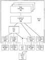
도 4는 CPU(402)와, 시스템 또는 "호스트" 브리지(404)와, 메모리(406)와, 제 1 디바이스 버스(408)(예를 들어, 주변 장치 구성요소 상호접속 또는 PCI 버스)와, 디바이스 버스 브리지(410)와, 제 2 디바이스 버스(412)(예를 들어, 산업 표준 아키텍쳐 또는 ISA 버스)와, 그리고 4개의 디바이스 하드웨어 유닛들(414A-414D)을 포함하는 컴퓨터 시스템(400)의 한 실시예도이다. 상기 호스트 브리지(404)는 상기 CPU(402)와, 메모리(406)와, 그리고 디바이스 버스(408)에 결합된다. 상기 호스트 브리지(404)는 상기 CPU(402)와 디바이스 버스(408) 간에 신호를 변환하고, 상기 메모리(406)를 상기 CPU(402)에 그리고 상기 디바이스 버스(408)에 동작가능하게 결합시킨다. 상기 디바이스 버스 브리지(410)는 상기 디바이스 버스(408)와 상기 디바이스 버스(412) 간에 결합되고, 상기 디바이스 버스(408)와 상기 디바이스 버스(412) 간에 신호들을 변환시킨다. 도 4의 실시예에서, 상기 디바이스 하드웨어 유닛들(414A-414B)이 상기 디바이스 버스(408)에 결합되고, 상기 디바이스 하드웨어 유닛들(414C-414D)이 상기 디바이스 버스(412)에 결합된다. 하나 이상의 상기 디바이스 하드웨어 유닛들(414A-414D)이 예를 들어, 저장 디바이스(예를 들어, 하드 디스크 드라이브들과, 플로피 디스크들과, 그리고 CD-ROM 드라이브들)와, 통신 디바이스(예를 들어, 모뎀 및 네트워크 어댑터들) 또는 입력/출력 디바이스들(예를 들어, 비디오 디바이스들과, 오디오 디바이스들과, 그리고 프린터들)일 수 있다.4 shows a
도 4의 실시예에서, 상기 CPU(402)는 CPU 보안 체크 유닛(security check unit: 이하 SCU)(416)을 포함하고 호스트 브리지(404)는 호스트 브리지 SCU(418)를 포함한다. 이하 상세히 설명될 바와같이, 상기 CPU SCU(416)는 상기 CPU(402)에 의해 발생된 허가되지 않은 엑세스(즉, "소프트웨어-개시-엑세스")로 부터 상기 메모리(406)를 보호하고 호스트 브리지 SCU(418)는 디바이스 하드웨어 유닛(414A-414D)에 의해 개시된 허가되지 않은 엑세스로 부터 메모리(406)를 보호한다. 주목할 사항으로, 다른 실시예들에서, 상기 호스트 브리지(404)가 도 4에 나타낸 바와같이 상기 CPU(402)의 일부분일 수 있다.In the embodiment of FIG. 4, the
도 5는 도 4의 컴퓨터 시스템(400)의 다수의 하드웨어와 소프트웨어 구성요소들 간의 관계도이다. 도 5의 실시예에서, 다수의 응용 프로그램들(500)과, 오퍼레이팅 시스템(502)과, 보안 커널(security kernel; 504)과, 그리고 디바이스 드라이버들(506A-506D)이 메모리(406)에 저장된다. 상기 다수의 응용 프로그램들(500)과, 상기 오퍼레이팅 시스템(502)과, 상기 보안 커널(504)과, 그리고 상기 디바이스 드라이버들(506A-506D)은 상기 CPU(402)에 의해 실행된 명령들을 포함한다. 상기 오퍼레이팅 시스템(502)은 상기 응용 프로그램들(500)이 가동하는 상부에 유저 인터페이스 및 소프트웨어 "플랫폼"(체제)을 제공한다. 상기 오퍼레이팅 시스템(502)은 또한 예를 들어, 파일 시스템 관리와, 처리 관리와, 그리고 입력/출력(I/O) 제어를 포함하는 기본 지원 기능을 제공할 수 있다.5 is a relationship diagram between a number of hardware and software components of the
상기 오퍼레이팅 시스템(502)은 또한 기본 보안 기능들을 제공할 수 있다. 예를들어, 상기 CPU(402)(도 4)는 ×86 명령 세트의 명령들을 실행하는 ×86 프로세서일 수 있다. 이 상황에서, 상기 CPU(402)가 특수한 하드웨어 요소(component)들을 포함하여 전술된 바와같은 보호 모드에서 가상 메모리 및 메모리 보호 특징들 둘다를 제공할 수 있다. 상기 오퍼레이팅 시스템(502)은 예를 들어, 상기 보호 모드에서 상기 CPU(402)를 동작시키는 Windows®패밀리의 오퍼레이팅 시스템(Microsoft Corp., Redmond, WA)중 하나일 수 있고 상기 CPU(402)의 상기 특수한 하드웨어 요소들을 사용하여 상기 보호 모드에서 가상 메모리와 메모리 보호 둘다를 제공한다.The
이하 보다 상세히 설명될 바와같이, 상기 보안 커널(504)은 상기 오퍼레이팅 시스템(502)에 의해 제공된 상기 보안 기능들 보다 뛰어난 추가 보안 기능들을 제공하여 허가되지 않은 엑세스로 부터 상기 메모리(406)에 저장된 데이타를 보호한다. 도 5의 실시예에서, 상기 디바이스 드라이버들(506A-506D)은 각기 대응하는 디바이스 하드웨어 유닛들(414A-414D)과 선택적으로 관련되고 결합된다. 상기 디바이스 하드웨어 유닛들(414A-414D)은 "보안(secure)" 디바이스이고, 대응하는 디바이스 드라이버들(506A-506D)은 "보안" 디바이스 드라이버이다. 상기 보안 커널(504)이 상기 오퍼레이팅 시스템(502)과 상기 안전한 디바이스 드라이버들(506A-506D) 간에 결합되고 상기 응용 프로그램들(500)과 상기 오퍼레이팅 시스템(502)에 의한 모든 엑세스들을 모니터하여, 상기 디바이스 드라이버들(506A-506D)과 상기 대응하는 보안 디바이스들(414A-414D)을 보안되게 한다. 상기 보안 커널(504)은 상기 응용 프로그램(500) 및 상기 오퍼레이팅 시스템(502)이 상기 보안 디바이스 드라이버들(506A-506D)과 상기 대응하는 보안 디바이스들(414A-414D)에의 허가없이 엑세스하는 것을 방지한다.As will be described in more detail below, the
도 5에 나타낸 바와같이, 상기 보안 커널(504)은 상기 CPU SCU(416) 및 호스트 브리지(SCU)(418)에 결합된다(예를 들어, 하나 이상의 디바이스 드라이버를 통해). 이하 상세히 설명될 바와같이, 상기 CPU SCU(416) 및 호스트 브리지 SCU (418)는 상기 메모리(406)로의 엑세스들을 제어한다. CPU SCU(416)은 메모리(406)로의 모든 소프트웨어-개시 엑세스들을 모니터하고, 호스트 브리지(SCU)(418)는 메모리(406)로의 모든 하드웨어-개시 엑세스들을 모니터한다. 보안 커널(504)에 의해 일단 설정되면, CPU SCU(416) 및 호스트 브리지(SCU)(418)는 허가된 엑세스만을 상기 메모리(406)에 허용한다.As shown in FIG. 5, the
도 5의 실시예에서, 상기 디바이스 드라이버들(506B-506C)이 "비보안(non-secure)" 디바이스 드라이버이고, 상기 대응하는 디바이스 하드웨어 유닛들(414B-414C)은 "비보안" 디바이스 하드웨어 유닛들이다. 상기 디바이스 드라이버들(506B-506C)은 및 상기 대응하는 디바이스 하드웨어 유닛들(414B-414C)은 예를 들어, "레가시(legacy)" 디바이스 드라이버들 및 디바이스 하드웨어 유닛들일 수 있다.In the embodiment of FIG. 5, the device drivers 506B-506C are "non-secure" device drivers, and the corresponding
주목할 사항으로, 다른 실시예들에선, 상기 보안 커널(504)이 상기 오퍼레이팅 시스템(502)의 일부분일 수 있다. 또다른 실시예에선, 상기 보안 커널(504)과, 상기 디바이스 드라이버들(506A-506D) 그리고/또는 상기 디바이스 드라이버들(506B-506C)이 상기 오퍼레이팅 시스템(502)의 일부분일 수 있다.Note that in other embodiments, the
도 6은 도 4의 컴퓨터 시스템(400)의 상기 CPU(402)의 한 실시예도이다. 도 6의 실시예에서, 상기 CPU(402)는 실행 유닛(600)과, 메모리 관리 유닛(MMU)(602)과, 캐시 유닛(604)과, 버스 인터페이스 유닛(Bus Interface Unit: 이하 BIU)(606)과, 한 세트의 제어 레지스터들(608)과, 그리고 한 세트의 보안 실행 모드(secure execution mode: 이하 SEM) 레지스터들(610)을 포함한다. 상기 CPU SCU(416)가 상기 MMU(602)내에 위치된다. 이하 상세히 설명될 바와같이, 상기 한 세트의 SEM 레지스터들(610)은 도 4의 컴퓨터 시스템(400)내에서 보안 실행 모드(SEM)를 구현하는데 사용되고, 상기 CPU SCU(416) 및 호스트 브리지(SCU)(418)의 동작은 상기 한 세트의 SEM 레지스터들(610)의 내용들에 의해 제어된다. SEM 레지스터들(610)은 상기 보안 커널(504; 도 5)에 의해 엑세스된다(즉, 상기 CPU SCU(416)에 기록되고 그리고/또는 CPU SCU(416)로 부터 판독된다). 도 4의 상기 컴퓨터 시스템(400)은, 예를 들어 (i) 상기 CPU(402)가 ×86 보호 모드에서 동작하는 ×86 프로세서일 때와, (ii) 메모리 페이징이 인에이블(enable)될 때와, 그리고 (iii) SEM 레지스터들(610)의 내용들이 SEM 동작을 한정할 때에, 상기 SEM에서 동작할 수 있다.6 is an embodiment diagram of the
일반적으로, 상기 한 세트의 제어 레지스터들(608)의 내용이 상기 CPU(402)의 동작을 제어한다. 따라서, 상기 한 세트의 제어 레지스터들(608)의 내용이 상기 실행 유닛(600)과, 상기 MMU(602)와, 상기 캐시 유닛(604)과, 그리고 상기 BIU(606)의 동작을 제어한다. 상기 한 세트의 제어 레지스터들(608)은 예를 들어, ×86 프로세서 아키텍쳐의 복수의 제어 레지스터들을 포함할 수 있다.In general, the contents of the set of control registers 608 control the operation of the
상기 CPU(402)의 실행 유닛(600)은 명령들(예를 들어, ×86 명령들) 및 데이타를 페치하고, 상기 페치된 명령들을 실행하고 명령 실행동안 신호들(예를 들어, 어드레스와, 데이타와, 그리고 제어 신호들)을 발생한다. 상기 실행 유닛(600)이 캐시 유닛(604)에 결합되고, 상기 캐시 유닛(604) 및 상기 BIU(606)을 통해 상기 메모리(406, 도 4)로 부터의 명령들을 수신할 수 있다.The
상기 컴퓨터 시스템(400)의 상기 메모리(406, 도 4)는 특정한 물리적 어드레스를 각각 가진 복수의 메모리 위치들을 포함한다. 인에이블된 페이징에 대해 보호 모드에서 동작할 때에, 상기 CPU(402)의 어드레스 공간은 페이지 프레임들 또는 "페이지들"이라고 불리는 복수의 블럭들로 분할된다. 앞서 설명된 바와같이, 상기 페이지들의 일부분에 대응하는 데이타만이 임의의 소정의 시간에 상기 메모리(406) 내에 저장된다. 도 6의 실시예에서, 명령 실행동안 상기 실행 유닛(600)에 의해 발생된 어드레스 신호들이 세그먼트(즉, "논리적(logical)") 어드레스들을 나타낸다. 이하 상세히 설명될 바와같이, 상기 MMU(602)는 상기 실행 유닛(600)에 의해 발생된 상기 세그먼트 어드레스들을 상기 메모리(406)의 대응하는 물리적 어드레스들로 변환한다. 상기 MMU(602)는 상기 물리적 어드레스들을 상기 캐시 유닛(604)에 제공한다. 상기 캐시 유닛(604)은 상기 실행 유닛(600)에 의해 최근에 페치된 명령들 및 데이타를 저장하는데 사용되는 비교적 작은 저장 유닛이다. 상기 BIU(606)이 상기 캐시 유닛(604)과 상기 호스트 브리지(404) 간에 결합되고, 상기 호스트 브리지(404)를 통해 상기 캐시 유닛(604)에 나타나지 않은 명령들과 데이타를 상기 메모리(406)로 부터 페치하는데 사용된다.The memory 406 (FIG. 4) of the
도 7은 도 6의 MMU(602)의 한 실시예도이다. 도 7의 실시예에서, 상기 MMU(602)는 분할(segmentation) 유닛(700)과, 페이징 유닛(702)과, 그리고 상기 분할 유닛(700) 및 상기 페이징 유닛(702)의 출력들 중 하나를 선택하여 물리적 어드레스를 생성하는 선택 논리(704)를 포함한다. 도 7에 도시된 바와같이, 상기 분할 유닛(700)은 상기 실행 유닛(600)으로부터 세그먼트 어드레스를 수신하고 상기 ×86 프로세서 아키텍쳐의 널리 공지된 세그먼트-대-선형 어드레스 변환 매카니즘을 사용하여, 대응하는 선형 어드레스를 출력에 생성시킨다. 도 7에 도시된 바와같이, "페이징(PAGING)" 신호에 의해 인에이블될 시에, 상기 페이징 유닛(702)은 상기 분할 유닛(700)에 의해 생성된 상기 선형 어드레스를 수신하고 대응하는 물리적 어드레스를 출력에서 생성한다. 상기 페이징 신호는 상기 ×86 프로세서 아키텍쳐와 상기 한 세트의 제어 레지스터들(608, 도 6)의 제어 레지스터 0(CR0)에 페이징 플래그(PG) 비트를 반영할 수 있다. 상기 페이징 신호가 디어서트(deassert)될 시에, 메모리 페이징이 인에이블되지 않고, 상기 선택 논리(704)는 상기 분할 유닛(700)으로부터 수신된 선형 어드레스를 물리적 어드레스로서 생성한다.FIG. 7 is an embodiment diagram of the
상기 페이징 신호가 어서트(assert)될 시에, 메모리 페이징이 인에이블되고 상기 페이징 유닛(702)은, 상기 ×86 프로세서 아키텍쳐(도 1)의 전술된 선형-대-물리적 어드레스 변환 매카니즘(100)을 사용하여, 상기 분할 유닛(700)으로부터 수신된 상기 선형 어드레스를 대응하는 물리적 어드레스로 변환시킨다. 전술된 바와같이, 상기 선형-대-물리적 어드레스 변환 동작 동안, 상기 선택된 페이지 디렉토리 엔트리 및 상기 선택된 페이지 테이블 엔트리의 상기 U/S 비트들의 내용들은 페이지 프레임으로의 엑세스가 허가되었는 지를 결정하기 위해 논리적으로 AND화된다. 마찬가지로, 상기 선택된 페이지 디렉토리 엔트리 및 상기 선택된 페이지 테이블 엔트리의 상기 R/W 비트들의 내용들도 페이지 프레임으로의 엑세스가 허가되었는 지를 결정하기 위해 논리적으로 AND화된다. 상기 U/S 및 R/W 비트들의 논리적 조합들이 상기 페이지 프레임으로의 엑세스가 허가되었음을 나타내면, 상기 페이징 유닛(702)은 상기 선형-대-물리적 어드레스 변환 동작으로부터 유래된 물리적 어드레스를 생성한다. 상기 선택 논리(704)는 상기 페이징 유닛(702)에 의해 생성된 상기 물리적 어드레스를 수신하며, 상기 페이징 유닛(702)로 부터 수신된 상기 물리적 어드레스를 물리적 어드레스로서 생성하고, 그 생성된 물리적 어드레스를 상기 캐시 유닛(604)에 제공한다.When the paging signal is asserted, memory paging is enabled and the paging unit 702 is configured with the aforementioned linear-to-physical
한편, 상기 U/S 및 R/W 비트들의 논리적 조합들이 상기 페이지 프레임으로의 엑세스가 허가되지 않았음을 나타내면, 상기 페이징 유닛(702)은 상기 선형-대-물리적 어드레스 변환 동작 동안 물리적 어드레스를 생성하지 못한다. 대신에, 상기 페이징 유닛(702)이 페이지 장애 신호를 어서트하고, 상기 MMU(602)가 상기 페이지 장애 신호를 상기 실행 유닛(600)으로 전송한다. 상기 ×86 프로세서 아키텍쳐에서, 일부 경우에, 페이지 장애 신호가 보호 위반을 나타낸다. 상기 페이지 장애 신호에 응답하여, 상기 실행 유닛(600)은 예외 처리기 루틴를 실행할 수 있고, 긍극적으로 상기 페이지 장애 신호가 어서트되었을 때 가동하는 응용 프로그램(500, 도 5)중 하나의 실행을 정지시킬 수 있다.On the other hand, if the logical combinations of the U / S and R / W bits indicate that access to the page frame is not allowed, the paging unit 702 generates a physical address during the linear-to-physical address translation operation. can not do. Instead, the paging unit 702 asserts a page fault signal, and the
도 7의 실시예에서, CPU SCU(416)는 MMU(602)의 페이징 유닛(702)내에 위치된다. 상기 페이징 유닛(702)은 또한 비교적 소수의 최근에 결정된 선형-대-물리적 어드레스 변환들을 저장하는 변환 색인 버퍼(traslation lookaside buffer:이하 TLB)를 포함할 수 있다.In the embodiment of FIG. 7, the
도 8은 도 7의 상기 CPU SCU(416)의 한 실시예도이다. 도 8의 실시예에서, 상기 CPU SCU(416)는 상기 한 세트의 SEM 레지스터들(610, 도 6)에 결합된 보안 체크 논리(800)와 보안 속성 테이블(Security Attribute Table: 이하 SAT) 엔트리 버퍼(802)를 포함한다. 이하 설명될 바와같이, SAT 엔트리는 메모리 페이지들에 대응하는 페이지 디렉토리 및 페이지 테이블 엔트리들의 상기 U/S 및 R/W 비트들을 비롯하여 추가의 보안 정보를 포함한다. 상기 보안 체크 논리(800)는 소정의 SAT 엔트리내에 기억된 추가의 보안 정보를 사용하여 대응하는 메모리 페이지로의 허가되지 않은 소프트웨어-개시 엑세스를 방지한다. 상기 SAT 엔트리 버퍼(802)는 최근에 엑세스된 메모리 페이지들의 비교적 소수의 SAT 엔트리들을 저장하는데 사용된다.FIG. 8 is an embodiment diagram of the
전술된 바와같이, 상기 한 세트의 SEM 레지스터들(610)은 도 4의 컴퓨터 시스템(400)내에 보안 실행 모드(SEM)를 구현하는데 사용된다. 상기 한 세트의 SEM 레지스터들(610)의 내용들은 상기 CPU SCU(416)의 동작을 제어한다. 상기 보안 체크 논리(800)는 도 8에 도시된 통신 버스를 통해 상기 MMU(602)로 부터 상기 SAT 엔트리 버퍼(802)에 기억되어질 정보를 수신한다. 상기 보안 체크 논리(800)는 또한 상기 페이징 유닛(702)에 의해 생성된 물리적 어드레스도 수신한다.As described above, the set of SEM registers 610 is used to implement a secure execution mode (SEM) in the
도 9 내지 도 11은 도 1의 어드레스 변환 매카니즘(100)을 사용하여 선택된 메모리 페이지의 추가 보안 정보가 도 4의 컴퓨터 시스템(400)내에서 어떻게 획득되는 지를 설명하는데 사용될 것이다. 도 9는 선택된 메모리 페이지의 추가 보안 정보를 획득하기 위해, 상기 선택된 메모리 페이지의 SAT 엔트리에 엑세스하기 위한 매카니즘(900)의 한 실시예도이다. 도 9의 매카니즘(900)은 도 8의 보안 체크 논리(800)내에서 실현되고, 도 4의 컴퓨터 시스템(400)이 상기 SEM에서 동작할 때 구현될 수 있다. 상기 매카니즘(900)은 도 1의 어드레스 변환 매카니즘(100)을 사용하여 페이징 매카니즘(702, 도 7)에 의해 생성된 물리적 어드레스(902)와, SAT 디렉토리(904)와, SAT(906)를 포함하는 복수의 SAT들과, 그리고 상기 SEM 레지스터들(610)의 SAT 기준 어드레스 레지스터(908)를 포함한다. 상기 SAT 디렉토리(904)와 상기 SAT(906)를 포함하는 복수의 SATs는 상기 보안 커널(504, 도 5)에 의해 발생되고 유지된 SEM 데이타 구조들이다. 이하 설명될 바와같이, 상기 SAT 디렉토리(904)(존재할 시에) 및 필요한 모든 SAT는 엑세스되기 전에 상기 메모리(406)내로 카피된다.9-11 will be used to illustrate how additional security information of a selected memory page using the
상기 SAT 기준 어드레스 레지스터(908)는 상기 SAT 기준 어드레스 레지스터(908)내에 유효한 SAT 디렉토리 기준 어드레스의 존재를 나타내는 존재(P) 비트를 포함한다. 상기 SAT 기준 어드레스 레지스터(908)의 최고 순위(즉, 최상위) 비트들은 상기 SAT 디렉토리 기준 어드레스 용으로 지정된다. 상기 SAT 디렉토리 기준 어드레스는 상기 SAT 디렉토리(904)를 포함하는 메모리 페이지의 기준 어드레스이다. 만약 P=1이면, 상기 SAT 디렉토리 기준 어드레스는 유효하며, SAT 테이블은 메모리 페이지들의 보안 속성들을 한정한다. 만약 P=0이면, 상기 SAT 디렉토리 기준 어드레스는 유효하지 않으며, 어떠한 SAT 테이블도 존재치 않고, 메모리 페이지들의 보안 속성들이 SAT 디폴트 레지스터에 의해 결정된다.The SAT reference address register 908 includes a presence (P) bit indicating the presence of a valid SAT directory reference address in the SAT reference address register 908. The most significant (ie, most significant) bits of the SAT reference address register 908 are designated for the SAT directory reference address. The SAT directory reference address is a reference address of a memory page that includes the
도 10은 SAT 디폴트 레지스터(1000)의 한 실시예도이다. 도 10의 실시예에서, 상기 SAT 디폴트 레지스터(1000)는 보안 페이지(SP) 비트를 포함한다. 상기 SP 비트는 모든 메모리 페이지들이 보안 페이지인 지의 여부를 나타낸다. 예를 들어, 만약 SP=0 이면, 모든 메모리 페이지들이 보안 페이지가 아니고, 만약 SP=1 이면, 모든 메모리 페이지들이 보안 페이지이다.10 is an embodiment diagram of the SAT default register 1000. In the embodiment of FIG. 10, the SAT default register 1000 includes secure page (SP) bits. The SP bit indicates whether all memory pages are secure pages. For example, if SP = 0, all memory pages are not secure pages, and if SP = 1, all memory pages are secure pages.
도 9를 재차 고려하고, SAT 기준 어드레스 레지스터(908)의 P 비트가 1이라고 가정하면, 상기 페이징 유닛(702, 도 7)에 의해 생성된 물리적 어드레스(902)는 3개의 부분들로 분할되어, 상기 선택된 메모리 페이지의 상기 SAT 엔트리에 엑세스한다. 전술된 바와같이, 상기 SAT 기준 어드레스 레지스터(908)의 상기 SAT 디렉토리 기준 어드레스가 상기 SAT 디렉토리(904)를 포함하는 메모리 페이지의 기준 어드레스이다. SAT 디렉토리(904)는 SAT 디렉토리 엔트리(910)를 포함하는 복수의 SAT 디렉토리 엔트리들을 포함한다. 각 SAT 디렉토리 엔트리는 상기 메모리(406)에 대응하는 SAT를 가질수 있다. 물리적 어드레스(902)의 최고 순위 또는 최상위 비트들을 포함하는 상기 물리적 어드레스(902)의 "상위" 부분은 상기 SAT 디렉토리(904)내에 색인으로서 사용된다. 상기 SAT 디렉토리 엔트리(910)는 상기 SAT 기준 어드레스 레지스터(908)의 상기 SAT 디렉토리 기준 어드레스와 상기 물리적 어드레스(902)의 상위 부분을 사용하여 상기 SAT 디렉토리(904)내에서 부터 선택된다.Referring back to FIG. 9 and assuming that the P bit of the SAT reference address register 908 is 1, the physical address 902 generated by the paging unit 702 (FIG. 7) is divided into three parts, Access the SAT entry of the selected memory page. As described above, the SAT directory reference address of the SAT reference address register 908 is the reference address of the memory page that contains the
도 11은 SAT 디렉토리 엔트리 포맷(1100)의 한 실시예도이다. 도 11에 따라, 각 SAT 디렉토리 엔트리는 상기 SAT 디렉토리 엔트리내에 유효한 SAT 기준 어드레스의 존재를 나타내는 존재(P) 비트를 포함한다. 도 11의 실시예에서, 각 SAT 디렉토리 엔트리의 상기 최고 순위(즉, 최상위) 비트들은 SAT 기준 어드레스용으로 지정된다. 상기 SAT 기준 어드레스는 대응하는 SAT를 포함하는 메모리 페이지의 기준 어드레스이다. 만약 P=1이면, 상기 SAT 기준 어드레스는 유효하며, 상기 대응하는 SAT가 상기 메모리(406)에 저장된다.11 is an embodiment diagram of a SAT directory entry format 1100. According to FIG. 11, each SAT directory entry includes a presence (P) bit indicating the presence of a valid SAT reference address in the SAT directory entry. In the embodiment of FIG. 11, the highest order (ie, most significant) bits of each SAT directory entry are designated for a SAT reference address. The SAT reference address is a reference address of a memory page containing a corresponding SAT. If P = 1, the SAT reference address is valid and the corresponding SAT is stored in the
만약 P=0이면, 상기 SAT 기준 어드레스는 유효하지 않으며, 상기 대응하는 SAT는 상기 메모리(406)에 존재하지 않고, 저장 디바이스(예를 들어, 디스크 드라이브)로 부터 상기 메모리(406)내로 카피되어야 한다. 만약 P=0이면, 상기 보안 체크 논리(800)는 논리로 페이지 장애를 페이징 유닛(702)에 신호하고, 상기 MMU(602)는 상기 페이지 장애 신호를 실행 유닛(600, 도 6)으로 전송한다. 상기 페이지 장애 신호에 응답하여, 상기 실행 유닛(600)은 상기 저장 장치로부터 요구된 SAT를 검색하는 페이지 장애 처리기 루틴을 실행시키고, 상기 요구된 SAT를 메모리(406)에 저장한다. 상기 요구된 SAT가 상기 메모리(406)에 저장된 후에, 대응하는 SAT 디렉토리 엔트리의 상기 P 비트가 '1'로 설정되고, 상기 매카니즘(900)이 계속된다.If P = 0, the SAT reference address is not valid and the corresponding SAT does not exist in the
도 9를 재차 고려해볼 때, 상기 물리적 어드레스(902)의 "중간" 부분이 SAT(906)내에서 색인으로서 사용된다. 따라서 상기 SAT 엔트리(906)는 상기 SAT 디렉토리 엔트리(910)의 SAT 기준 어드레스 및 상기 물리적 어드레스(902)의 상기 중간 부분을 사용하여 상기 SAT(906)내에서 선택된다. 도 12는 SAT 엔트리 포맷(1200)의 한 실시예도이다. 도 12의 실시예에서, 각 SAT 엔트리는 보안 페이지(SP) 비트를 포함한다. 상기 SP 비트는 선택된 메모리 페이지가 보안 페이지인 지의 여부를 나타낸다. 예를 들어, 만약, SP=0 이면, 상기 선택된 메모리 페이지는 보안 페이지가 아니고, 만약 SP=1 이면, 상기 선택된 메모리 페이지는 보안 페이지이다.Reconsidering FIG. 9, the "middle" portion of the physical address 902 is used as an index within the SAT 906. Thus, the SAT entry 906 is selected within the SAT 906 using the SAT reference address of the SAT directory entry 910 and the intermediate portion of the physical address 902. 12 is an embodiment diagram of a SAT entry format 1200. In the embodiment of Figure 12, each SAT entry includes a secure page (SP) bit. The SP bit indicates whether the selected memory page is a secure page. For example, if SP = 0, the selected memory page is not a secure page; if SP = 1, the selected memory page is a secure page.
상기 BIU(606, 도 6)는 상기 메모리(406)로 부터 요구된 SEM 데이타 구조 엔트리들을 검색하고 상기 SEM 데이타 구조 엔트리들을 상기 MMU(602)에 제공한다. 도 8을 재차 고려해볼 때, 상기 보안 체크 논리(800)는 통신 버스를 통해 상기 MMU(602) 및 상기 페이징 유닛(702)으로부터 SEM 데이타 구조 엔트리들을 수신한다. 전술된 바와같이, 상기 SAT 엔트리 버퍼(802)는 최근에 엑세스된 메모리 페이지들의 비교적 소수의 SAT 엔트리들을 저장하는데 사용된다. 상기 보안 체크 논리(800)는 대응하는 물리적 어드레스의 "태그(tag)" 부분을 따라 상기 SAT 엔트리 버퍼(802)에 소정의 SAT 엔트리를 저장시킨다.The BIU 606 (FIG. 6) retrieves the required SEM data structure entries from the
후속의 메모리 페이지 엑세스 동안, 상기 보안 체크 논리(800)는 상기 페이징 유닛(702)에 의해 생성된 물리적 어드레스의 "태그" 부분을 상기 SAT 엔트리 버퍼(802)에 저장된 SAT 엔트리에 대응하는 물리적 어드레스의 태그 부분들과 비교한다. 상기 물리적 어드레스의 상기 태그 부분이 상기 SAT 엔트리 버퍼(802)내의 SAT 엔트리에 대응하는 물리적 어드레스의 태그 부분과 부합하면, 상기 보안 체크 논리(800)는 SAT 엔트리 버퍼(802)에 저장된 SAT 엔트리에 엑세스하며, 도 9의 메모리(406)으로부터 상기 SAT 엔트리를 획득하는 프로세스를 수행할 필요를 제거한다. 상기 보안 커널(504, 도 5)은 상기 CPU(402)의 상기 SAT 기준 어드레스 레지스터(908)의 내용들을 변경한다(예를 들어, 문맥 교환(context switch)시에). 상기 SAT 기준 어드레스 레지스터(908)의 변경에 응답하여, 상기 CPU SCU(416)의 상기 보안 체크 논리(800)는 상기 SAT 엔트리 버퍼(802)를 플러쉬(flush)한다.During subsequent memory page accesses, the
도 4의 컴퓨터 시스템(400)이 상기 SEM에서 동작할 때, 상기 보안 체크 논리(800)는 페이지 디렉토리 엔트리(Page Directory Entry: 이하 PDE) U/S 비트와, PDE R/W 비트와, 페이지 테이블 엔트리(Page Table Entry: 이하 PTE) U/S 비트와, 그리고 PTE R/W 비트와 함께, 현재의 실행 과업(즉, 현재의 실행 명령)의 현재의 특권 레벨(CPL)을 수신한다. 상기 보안 체크 논리(800)는, 상기 선택된 메모리 페이지에 대응하는 상기 SAT 엔트리의 SP 비트와 함께 상기 정보를 이용하여, 상기 메모리(406) 엑세스가 허가되었는 지를 결정한다.When the
도 6의 상기 CPU(402)는 ×86 프로세서일 수도 있고 ×86 프로세서 아키텍쳐의 16 비트 세그먼트중 하나인 코드 세그먼트(CS) 레지스터를 포함할 수도 있다. 각 세그먼트 레지스터는 세그먼트라 칭해지는 64k 메모리 블럭을 선택한다. 인에이블된 페이징을 가진 보호 모드에서, 상기 CS 레지스터는 상기 메모리(406)의 실행가능한 세그먼트를 나타내는 세그먼트 선택기(segment selector)로 로드된다. 상기 세그먼트 선택기의 최고 순위(즉, 최상위) 비트들은 상기 CPU(402, 도 4)의 실행 유닛(600)에 의해 실행되어질 다음 명령을 포함하는 메모리 세그먼트를 나타내는 정보를 저장하는데 사용된다. 명령 포인터(IP) 레지스터는 상기 CS 레지스터에 의해 나타낸 세그먼트내에 오프셋(offset)을 저장하는데 사용된다. 상기 CS:IP 쌍은 상기 다음 명령의 세그먼트 어드레스를 나타낸다. 상기 CS 레지스터의 2개의 최고 하위(즉, 최하위) 비트들은 상기 실행 유닛(600)에 의해 현재 실행되는 과업의 현재의 특권 레벨(CPL)을 나타내는 값(즉, 현재의 과업의 CPL)을 저장하는데 사용된다.The
표 1은 도 4의 컴퓨터 시스템(400)이 SEM에서 동작할 시에, CPU-개시(즉, 소프트웨어-개시) 메모리 엑세스에 대한 예시적인 룰들을 나타낸다. 상기 CPU SCU(416, 도 4 내지 도 8) 및 상기 보안 커널(504, 도 5)은 도 4의 컴퓨터 시스템(400)이 SEM에서 동작할 시에, 표 1의 룰들을 함께 수행하여, 상기 메모리(406)에 저장된 데이타에 상기 오퍼레이팅 시스템(502, 도 5)에 의해 제공된 데이타 보안이상의 추가의 보안을 제공한다.Table 1 shows example rules for CPU-initiated (ie, software-initiated) memory access when the
표 1, 도 4의 컴퓨터 시스템(400)이 SEM 에서 동작할 때Table 1, when the
소프트웨어-개시 메모리 엑세스에 대한 예시적인 룰들Example Rules for Software-Initiated Memory Access
상기 표 1에서, 현재 실행중인 명령의 SP 비트는 상기 현재 실행중인 명령을 포함하는 메모리 페이지에 대응하는 SAT 엔트리의 SP 비트이다. 상기 선택된 메모리 페이지의 상기 U/S 비트는 상기 선택된 메모리 페이지의 상기 PDE U/S 비트 및 PTE U/S 비트의 논리적 AND이다. 상기 선택된 메모리 페이지의 상기 R/W 비트는 상기 선택된 메모리 페이지의 상기 PDE R/W 비트 및 PTE R/W 비트의 논리적 AND이다. 기호 "X"는 "돈 케어(don't care:상관 없음)"를 의미하며; 그 논리값은 '0'이나 또는 '1'일 수 있다.In Table 1, the SP bits of the currently executing instruction are the SP bits of the SAT entry corresponding to the memory page containing the currently executing instruction. The U / S bit of the selected memory page is a logical AND of the PDE U / S and PTE U / S bits of the selected memory page. The R / W bit of the selected memory page is the logical AND of the PDE R / W bit and the PTE R / W bit of the selected memory page. The symbol "X" means "don't care"; The logical value may be '0' or '1'.
도 8을 재차 고려해볼 때, 상기 CPU SCU(416)의 보안 체크 논리(800)는 페이지 장애 신호 및 "SEM SECURITY EXCEPTION" 신호를 생성하고 페이징 유닛(702)내에 논리로 상기 페이지 장애 및 상기 SEM SECURITY EXCEPTION을 제공한다. 상기 보안 체크 논리(800)가 상기 페이지 장애 신호를 어서트할 시에, 상기 MMU(602)는 상기 페이지 장애 신호를 상기 실행 유닛(600, 도 6)에 전송한다. 상기 페이지 장애 신호에 응답하여, 상기 실행 유닛(600)은 상기 ×86 프로세서 아키텍쳐의 널리-공지된 인터럽트 디스크립터 테이블(Interrupt Descriptor Table: 이하 IDT) 벡터링(vectoring) 매카니즘을 사용하여 페이지 장애 처리기 루틴(page fault handler routine)을 엑세스 및 실행한다.Referring back to FIG. 8, the
상기 보안 체크 논리(800)가 상기 SEM SECURITY EXCEPTION 신호를 어서트할 시에, 상기 MMU(602)는 상기 SEM SECURITY EXCEPTION 신호를 상기 실행 유닛(600)에 전송한다. 상기 ×86 프로세서 아키텍쳐의 IDT 벡터링 매카니즘을 사용하는 정규 프로세서 예외들과는 달리, 상이한 벡터링 방법이 SEM 보안 예외들을 처리하기 위해 사용될 수도 있다. SEM 보안 예외들은 x86 "SYSENTER" 및 "SYSEXIT" 명령들이 동작하는 방식과 유사한 방식으로 한 쌍의 레지스터들(예를 들어, 모델 특정 레지스터들(model specific register) 또는 MSRs)을 통해 디스페치(dispatch)될 수도 있다. 상기 한 쌍의 레지스터들은 "보안 예외 엔트리 포인트(security exception entry)" 레지스터들일 수 있고 SEM 보안 예외가 발생할 시에 명령 실행을 위한 분기 목표 어드레스(Branch Target Address)를 정의할 수도 있다. 상기 보안 예외 엔트리 포인트 레지스터들은 SEM 보안 예외 처리기에 엔트리로 사용되어질 코드 세그먼트(CS)와, 명령 포인터(IP, 또는 64-비트 버젼 RIP)와, 스택 세그먼트(SS)와, 그리고 스택 포인터(SP, 또는 64-비트 버젼 RSP)값들을 정의할 수 있다. 소프트웨어 제어하에서, 상기 실행 유닛(600, 도 6)은 앞서의 SS, SP/RSP, EFLAGS, CS 및 IP/RIP 값들을 새로운 스택상에 밀어넣어 어디서 예외가 발생하는 지를 나타낸다. 또한, 상기 실행 유닛(600)은 상기 스택상에 에러 코드를 밀어넣을 수도 있다. 주목할 사항으로, 인터럽트로부터의 정규 리턴(IRET) 명령은 CPL의 변경이 일어나지 않더라도, 상기 앞서의 SS 및 SP/RSP 값들이 항상 세이브되고 스택 스위치가 항상 달성되기에 사용되지 않는다. 따라서, 새로운 명령이 정의되어 상기 SEM 보안 예외 처리기로 부터의 리턴을 달성할 수 있다.When the
도 13은 도 4의 호스트 브리지(404)의 한 실시예도이다. 도 13의 실시예에서, 호스트 브리지(404)는 호스트 인터페이스(1300)과, 브리지 논리(1302)와, 호스트 브리지 SCU(418)와, 메모리 제어기(1304)와, 그리고 디바이스 버스 인터페이스(1306)를 포함한다. 호스트 인터페이스(1300)가 CPU(402)에 결합되고, 디바이스 버스 인터페이스(1306)가 디바이스 버스(408)에 결합된다. 브리지 논리(1302)가 호스트 인터페이스(1300)와 디바이스 버스 인터페이스(1306) 간에 결합된다. 메모리 제어기(1304)가 메모리(406)에 결합되어, 메모리(406)로의 모든 엑세스를 수행한다. 호스트 브리지 SCU(418)가 브리지 논리(1302)와 메모리 제어기(1304) 간에 결합된다. 전술된 바와같이, 호스트 브리지 SCU (418)가 디바이스 버스 인터페이스(1306)를 통하여 메모리(406)로의 엑세스를 제어한다. 호스트 브리지 SCU(418)는 디바이스 버스 인터페이스(1306)를 통하여 메모리(406)로의 모든 엑세스들을 모니터하고, 허가된 엑세스들만을 메모리(406)에 허용한다.FIG. 13 is an embodiment diagram of the
도 14는 도 13의 호스트 브리지 SCU(418)의 한 실시예도이다. 도 14의 실시예에서, 호스트 브리지 SCU(418)는 한 세트의 SEM 레지스터들(1402)과 SAT 엔트리 버퍼(1404)에 결합되는 보안 체크 논리(1400)를 포함한다. 상기 한 세트의 SEM 레지스터들(1402)은 보안 체크 논리(1400)의 동작을 제어하고, 도 9의 제 2의 SAT 기준 어드레스 레지스터(908)를 포함한다. 상기 한 세트의 SEM 레지스터들(1402)의 상기 제 2의 SAT 기준 어드레스 레지스터(908)는 어드레스가능한 레지스터일 수도 있다. 보안 커널(504, 도 5)이 CPU(402)의 상기 한 세트의 SEM 레지스터들(1402)내의 SAT 기준 어드레스 레지스터(908)의 내용들을 변경할 시에(예를 들어, 상황이 바뀌는 동안), 보안 커널(504)은 또한 호스트 브리지 SCU(418)의 상기 한 세트의 SEM 레지스터들(1402)내의 상기 제 2의 SAT 기준 어드레스 레지스터(908)에 동일한 값을 기록할 수도 있다. 상기 제 2의 SAT 기준 어드레스 레지스터(908)의 변경에 응답하여, 호스트 브리지 SCU(418)의 보안 체크 논리(1400)가 SAT 엔트리 버퍼(1404)를 플러쉬할 수도 있다.FIG. 14 is an embodiment diagram of the
보안 체크 논리(1400)는 디바이스 버스 인터페이스(1306)와 브리지 논리(1302, 도 13)를 통하여 하드웨어 디바이스 유닛들(414A-414D, 도 4)에 의해 개시된 메모리 엑세스의 메모리 엑세스 신호들을 수신한다. 상기 메모리 엑세스 신호들이 하드웨어 디바이스 유닛들(414A-414D)로 부터의 물리적 어드레스와, 관련 제어 그리고/또는 데이타 신호들을 운반한다. 보안 체크 논리(1400)는 대응하는 메모리 페이지의 SAT 엔트리들을 획득하기 위한 매카니즘(900, 도 9)을 실시할 수도 있고, 도 4의 컴퓨터 시스템(400)이 SEM 에서 동작할 시에, 매카니즘(900)을 구현할 수도 있다. SAT 엔트리 버퍼(1404)는 전술된 CPU SCU(416, 도 8)의 SAT 엔트리 버퍼(802)와 유사하고, 최근에 엑세스된 메모리 페이지들의 비교적 소수의 SAT 엔트리들을 저장하는데 사용된다.The
도 4의 컴퓨터 시스템(400)이 SEM 에서 동작할 시에, 도 14의 보안 체크 논리(1400)는 선택된 메모리 페이지와 관련된 SAT 엔트리의 추가의 보안 정보를 사용하여, 소정의 하드웨어-개시 메모리 엑세스가 허가되는 지를 결정한다. 소정의 하드웨어-개시 메모리 엑세스가 허가되면, 보안 체크 논리(1400)는 상기 메모리 엑세스의 상기 메모리 엑세스 신호들(예를 들어, 물리적 어드레스 및 관련 제어 그리고/또는 데이타 신호들을 운반하는 어드레스 신호들)을 메모리 제어기(1304)에 제공한다. 메모리 제어기(1304)는 상기 물리적 어드레스 및 관련 제어 그리고/또는 데이타 신호들을 사용하여 메모리(406)에 엑세스한다. 메모리(406) 엑세스가 기록 엑세스이라면, 상기 데이타 신호들에 의해 운반된 데이타가 메모리(406)에 기록된다. 메모리(406)에의 엑세스가 판독 엑세스이라면, 메모리 제어기(1304)는 메모리(406)로 부터의 데이타를 판독하고, 결과로서 발생한 판독 데이타를 보안 체크 논리(1400)에 제공한다. 보안 체크 논리(1400)는 상기 판독 데이타를 브리지 논리(1302)로 전송하고, 브리지 논리(1302)는 상기 데이타를 디바이스 버스 인터페이스(1306)에 제공한다.When the
한편, 상기 소정의 하드웨어-개시 메모리 엑세스가 허가되지 않는다면, 보안 체크 논리(1400)는 메모리(406)의 물리적 어드레스 및 관련 제어 그리고/또는 데이타 신호들을 메모리 제어기(1304)에 제공하지 못한다. 허가되지 않은 하드웨어-개시 메모리 엑세스가 메모리 기록 엑세스이라면, 보안 체크 논리(1400)는 기록 엑세스의 완료를 신호하고, 메모리(406)를 변경하지않은채 기록 데이타를 버린다. 보안 체크 논리(1400)는 또한 로그(log)에 로그 엔트리를 형성하여(예를 들어, 상태 레지스터의 하나 이상의 비트들을 설정 또는 소거), 보안 엑세스 위반을 기록한다. 보안 커널(504)은 상기 로그를 주기적으로 엑세스하여 이러한 로그 엔트리들에 대해 체크한다. 허가되지 않은 하드웨어-개시 메모리 엑세스가 메모리 판독 엑세스이라면, 보안 체크 논리(1400)는 틀린 결과(예를 들어, 모두 "F")를 판독 데이타로서 브리지 논리(1302)를 통하여 디바이스 버스 인터페이스(1306)로 리턴할 수 있다. 보안 체크 논리(1400)는 또한 전술된 바와같은 로그 엔트리를 형성하여 보안 엑세스 위반을 기록할 수 있다.On the other hand, if the predetermined hardware-initiated memory access is not granted, the
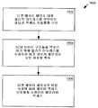
도 15는 복수의 메모리 페이지들내에 배열된 데이타를 저장하기 위해 사용된 메모리에 대한 엑세스 보안을 제공하는 방법(1500)의 한 실시예의 흐름도이다. 상기 방법(1500)은 도 4의 컴퓨터 시스템(400)이 상기 SEM에서 동작할 시에 CPU-개시(즉, 소프트웨어-개시) 메모리 엑세스들에 대한 표 1의 예시적인 룰들을 반영한다. 상기 방법(1500)은 상기 MMU(602, 도 6-7)내에서 실시될 수도 있다. 상기 방법(1500)의 단계(1502) 동안, 명령의 실행 동안 생성된 선형 어드레스가 상기 명령의 보안 속성들(예를 들어, 상기 명령을 포함하는 과업의 CPL)과 함께 수신된다. 상기 명령은 메모리 페이지에 상주한다. 단계(1504) 동안, 선형 어드레스가 상기 메모리에 위치된 적어도 하나의 페이지 메모리 데이타 구조(예를 들어, 페이지 디렉토리 및 페이지 테이블)에 엑세스하는데 사용되어, 상기 선택된 메모리 페이지의 기준 어드레스 및 상기 선택된 메모리 페이지의 보안 속성들을 획득한다. 상기 선택된 메모리 페이지의 상기 보안 속성들은 예를 들어, 페이지 디렉토리 엔트리의 U/S 비트 및 R/W 비트와 페이지 테이블 엔트리의 U/S 비트 및 R/W 비트를 포함한다.15 is a flow diagram of one embodiment of a
결정 단계(1506) 동안, 상기 명령의 상기 보안 속성 및 상기 선택된 메모리 페이지의 상기 보안 속성들은 엑세스가 허가되었는 지의 여부를 결정하는데 사용된다. 만약 상기 엑세스가 허가되었다면, 상기 선택된 메모리 페이지의 기준 어드레스 및 오프셋이 단계(1508) 동안 조합되어 상기 선택된 메모리 페이지 내의 물리적 어드레스를 생성한다. 만약 상기 엑세스가 허가되지 않았다면, 장애 신호(예를 들어, 페이지 장애 신호)가 단계(1510) 동안 발생된다.During decision step 1506, the security attributes of the command and the security attributes of the selected memory page are used to determine whether access is granted. If the access is granted, the reference address and offset of the selected memory page are combined during step 1508 to generate a physical address within the selected memory page. If the access is not granted, a fault signal (eg, a page fault signal) is generated during
단계(1508)에 뒤이은 단계(1512) 동안, 상기 메모리에 위치된 적어도 하나의 보안 속성 데이타 구조(도 9의 상기 SAT 디렉토리(904) 및 SAT)가 선택된 메모리 페이지의 물리적 어드레스를 사용하여 엑세스되어, 상기 제 1 메모리 페이지의 추가의 보안 속성 및 상기 선택된 메모리 페이지의 추가의 보안 속성을 획득한다. 상기 제 1 메모리 페이지의 추가의 보안 속성은 예를 들어, 전술된 바와같은 보안 페이지(SP) 비트를 포함하며, 여기서 상기 SP 비트는 상기 제 1 메모리 페이지가 보안 페이지인 지의 여부를 나타낸다. 마찬가지로, 상기 선택된 메모리 페이지의 추가의 보안 속성은 보안 페이지(SP) 비트를 포함하며, 여기서 상기 SP 비트는 상기 선택된 메모리 페이지가 보안 페이지인 지의 여부를 나타낸다.During
장애 신호는 명령의 보안 속성과, 제 1 메모리 페이지의 추가의 보안 속성과, 선택된 메모리 페이지의 보안 속성들과, 그리고 선택된 메모리 페이지의 추가의 보안 속성에 따라 단계(1514) 동안 발생된다. 방법(1500)의 단계들(1512 및 1514)이 CPU SCU(416, 도 4-8)내에서 실시될 수도 있다는 것에 주목해야 한다.The fault signal is generated during
이하 표 2는 도 4의 컴퓨터 시스템(400)이 SEM에서 동작할 시에, 디바이스 하드웨어 유닛들(414A-414D)에 의해 개시된 메모리 페이지 엑세스들(즉, 하드웨어-개시 메모리 엑세스들)에 대한 예시적인 룰들을 도시한다. 이러한 하드웨어-개시 메모리 엑세스들은 디바이스 하드웨어 유닛들(414A-414D)내에서 버스 마스터 회로 소자에 의해서나 또는 디바이스 하드웨어 유닛들(414A-414D)의 요구로 DMA 디바이스에 의해서 개시될 수도 있다. 보안 체크 논리(1400)는 도 4의 컴퓨터 시스템(400)이 SEM에서 동작할 시에, 표 2의 룰들을 구현하여, 오퍼레이팅 시스템(502, 도 5)에 의해 제공된 데이타 보안 이상으로 메모리(406)에 저장된 데이타에 대한 추가의 보안을 제공한다. 이하 표 2에서, "타겟" 메모리 페이지는 메모리 엑세스의 메모리 엑세스 신호들에 의해 운반된 물리적 어드레스가 상주하는 메모리 페이지이다.Table 2 below illustrates exemplary memory page accesses (ie, hardware-initiated memory accesses) initiated by the
표 2, 도 4의 컴퓨터 시스템(400)이 SEM 에서 동작할 때Table 2, when the
하드웨어-개시 메모리 엑세스에 대한 예시적인 룰들Example Rules for Hardware-Initiated Memory Access
상기 표 2에서, 타겟 메모리 페이지의 SP 비트는 메모리 엑세스의 물리적 어드레스 및 대응하는 메모리 페이지들의 SAT 엔트리들을 획득하기 위한 도 9의 전술된 매카니즘(900)을 사용하여 호스트 브리지 SCU(418)에 의해 획득된다.In Table 2 above, the SP bits of the target memory page are obtained by the
도 2에 도시된 바와같이, 타겟 메모리 페이지를 나타내는 SP=1이 보안 페이지일 시에, 메모리 엑세스가 허가되지 않는다. 상기 상황에서, 보안 체크 논리(1400, 도 14)는 메모리 제어기에 메모리 엑세스 신호들을 제공하지 않는다. 상기 메모리 엑세스 신호들(예를 들어, 제어 신호들)의 일부가 메모리 엑세스 형태를 나타내고, 상기 메모리 엑세스 형태는 판독 엑세스나 또는 기록 엑세스 중 어느 하나이다. SP=1이고 메모리 엑세스 신호들이 메모리 엑세스 형태가 판독 엑세스임을 나타낼 때, 상기 메모리 엑세스는 허가되지 않은 판독 엑세스이고, 보안 체크 논리(1400)는 실제 메모리 내용들 대신에 모두 "F"(즉, 가짜(bogus) 판독 데이타)를 제공함으로써 허가되지 않은 판독 엑세스에 응답한다. 보안 체크 논리(1400)는 또한 전술된 바와같은 허가되지 않은 판독 엑세스를 로깅함으로써 허가되지 않은 판독 엑세스에 응답할 수도 있다.As shown in Fig. 2, when SP = 1 indicating a target memory page is a secure page, memory access is not permitted. In this situation, security check logic 1400 (FIG. 14) does not provide memory access signals to the memory controller. Some of the memory access signals (e.g., control signals) represent a memory access form, and the memory access form is either a read access or a write access. When SP = 1 and the memory access signals indicate that the memory access type is a read access, the memory access is an unauthorized read access, and the
SP=1이고 메모리 엑세스 신호들이 메모리 엑세스 형태가 기록 엑세스임을 나타낼 때, 상기 메모리 엑세스는 허가되지 않은 기록 엑세스이다. 이 상황에서, 보안 체크 논리(1400)는 메모리 엑세스 신호들에 의해 운반된 기록 데이타를 버림으로써 허가되지 않은 기록 엑세스에 응답한다. 보안 체크 논리(1400)는 또한 전술된 바와같은 허가되지 않은 기록 엑세스를 로깅함으로써 허가되지 않은 기록 엑세스에 응답할 수도 있다.When SP = 1 and the memory access signals indicate that the memory access type is a write access, the memory access is an unauthorized write access. In this situation,
도 16은 다수의 메모리 페이지들내에 배치된 데이타를 저장하는데 사용된 메모리에 대한 엑세스 보안을 제공하기 위한 방법(1600)의 한 실시예의 흐름도이다. 방법(1600)은 도 4의 컴퓨터 시스템(400)이 SEM에서 동작할 시에, 하드웨어-개시 메모리 엑세스들에 대한 표 2의 예시적인 룰들을 반영한다. 방법(1600)은 호스트 브리지(404)(도 4 및 도 13-14)내에서 실시될 수도 있다. 방법(1600)의 단계(1602) 동안, 메모리 엑세스의 메모리 엑세스 신호들이 수신되는바, 여기서 상기 메모리 엑세스 신호들은 타겟 메모리 페이지 내의 물리적 어드레스를 운반한다. 전술된 바와같이, 상기 메모리 엑세스 신호들은 디바이스 하드웨어 유닛에 의해 생성될 수도 있다. 상기 물리적 어드레스는 상기 메모리에 위치된 적어도 하나의 보안 속성 데이타 구조에 엑세스하는데 사용되어, 단계(1604) 동안 상기 타겟 메모리 페이지의 보안 속성을 획득한다. 상기 적어도 하나의 보안 속성 데이타 구조는 예를 들어, SAT 디렉토리(예를 들어, 도 9의 SAT 디렉토리(904))와, 적어도 하나의 SAT(예를 들어, 도 9의 SAT(906))를 포함하고, 그리고 타겟 메모리 페이지의 추가적인 보안 속성은 상기 타겟 메모리 페이지가 보안 페이지인 지의 여부를 나타내는 전술된 바와같은 보안 페이지(SP) 비트를 포함할 수도 있다. 단계(1606) 동안, 상기 메모리는 상기 타겟 메모리 페이지의 보안 속성에 따른 상기 메모리 엑세스 신호들을 사용하여 엑세스된다. 방법(1600)의 단계들(1600 및 1602)이 호스트 브리지 SCU (418)(도 4 및 도 13-14)내에서 실시될 수도 있다는 것에 주목해야 한다.16 is a flow diagram of one embodiment of a
전술된 상기 특정 실시예들은 단지 설명만을 위한 것이며, 본원에 교시하는 잇점을 가진 이 분야의 기술에 숙련된 자에게는 본 발명이 상이하나 균등한 방식으로 변경 및 실시될 수 있음이 명백할 것이다. 또한, 본 발명은 본원에 나타낸 구성 및 설계에 제한 되지 않고 이하 청구범위에 설명된 바와같이 제한하고자 의도된다. 그러므로 전술된 상기 특정 실시예들은 변경 또는 변형될 수 있으며, 모든 이러한 변형들 은 본 발명의 범위와 정신내에서 고려될 수 있음은 당연하다. 따라서 본원에서 보호하고자 하는 것은 이하 청구범위에 설정된 바와같다.The specific embodiments described above are for illustrative purposes only, and it will be apparent to those skilled in the art having the benefit taught herein that the present invention may be modified and practiced in different but equivalent ways. In addition, the present invention is not intended to be limited to the construction and design shown herein but is to be limited as described in the claims below. Therefore, it is obvious that the specific embodiments described above may be changed or modified, and all such modifications may be considered within the scope and spirit of the present invention. Therefore, what is intended to be protected herein is as set forth in the claims below.
Claims (10)
Translated fromKoreanApplications Claiming Priority (2)
| Application Number | Priority Date | Filing Date | Title |
|---|---|---|---|
| US10/011,151US7426644B1 (en) | 2001-12-05 | 2001-12-05 | System and method for handling device accesses to a memory providing increased memory access security |
| US10/011,151 | 2001-12-05 |
Publications (2)
| Publication Number | Publication Date |
|---|---|
| KR20050027085A KR20050027085A (en) | 2005-03-17 |
| KR100995146B1true KR100995146B1 (en) | 2010-11-18 |
Family
ID=21749091
Family Applications (1)
| Application Number | Title | Priority Date | Filing Date |
|---|---|---|---|
| KR1020047008690AExpired - Fee RelatedKR100995146B1 (en) | 2001-12-05 | 2002-09-12 | System and method for controlling device access to memory providing improved memory access security |
Country Status (9)
| Country | Link |
|---|---|
| US (1) | US7426644B1 (en) |
| JP (1) | JP2005512228A (en) |
| KR (1) | KR100995146B1 (en) |
| CN (1) | CN1285038C (en) |
| AU (1) | AU2002336493A1 (en) |
| DE (1) | DE10297494T5 (en) |
| GB (1) | GB2399920B (en) |
| TW (1) | TWI262389B (en) |
| WO (1) | WO2003050688A2 (en) |
Families Citing this family (21)
| Publication number | Priority date | Publication date | Assignee | Title |
|---|---|---|---|---|
| EP1619572A1 (en)* | 2004-07-23 | 2006-01-25 | Texas Instruments Incorporated | System and method of identifying and preventing security violations within a computing system |
| DE102005014837B4 (en)* | 2004-08-02 | 2007-08-30 | Mahltig, Holger | Security module and method for controlling and controlling a data traffic of a personal computer |
| JP4794269B2 (en)* | 2004-11-08 | 2011-10-19 | パナソニック株式会社 | Secure device and relay terminal |
| JP4628149B2 (en)* | 2005-03-14 | 2011-02-09 | 株式会社エヌ・ティ・ティ・ドコモ | Access control apparatus and access control method |
| TWI310153B (en) | 2006-08-17 | 2009-05-21 | Quanta Comp Inc | Computer system and boot code accessing method thereof |
| TWI448902B (en)* | 2007-08-24 | 2014-08-11 | Cypress Semiconductor Corp | Bridge device with page access base processor interface |
| US8578483B2 (en)* | 2008-07-31 | 2013-11-05 | Carnegie Mellon University | Systems and methods for preventing unauthorized modification of an operating system |
| TWI484334B (en)* | 2009-12-24 | 2015-05-11 | Univ Nat Taiwan | Method for region-based management of non-volatile memory |
| US20110202740A1 (en)* | 2010-02-17 | 2011-08-18 | Arm Limited | Storing secure page table data in secure and non-secure regions of memory |
| US8935800B2 (en) | 2012-12-31 | 2015-01-13 | Intel Corporation | Enhanced security for accessing virtual memory |
| US8959576B2 (en)* | 2013-03-14 | 2015-02-17 | Intel Corporation | Method, apparatus, system for qualifying CPU transactions with security attributes |
| US9767044B2 (en)* | 2013-09-24 | 2017-09-19 | Intel Corporation | Secure memory repartitioning |
| CN104169891B (en)* | 2013-10-29 | 2017-07-21 | 华为技术有限公司 | A kind of method and apparatus for accessing internal memory |
| US9875189B2 (en) | 2015-06-12 | 2018-01-23 | Intel Corporation | Supporting secure memory intent |
| US20170109526A1 (en)* | 2015-10-20 | 2017-04-20 | Intel Corporation | Systems and methods for providing anti-malware protection and malware forensics on storage devices |
| US12248560B2 (en)* | 2016-03-07 | 2025-03-11 | Crowdstrike, Inc. | Hypervisor-based redirection of system calls and interrupt-based task offloading |
| US12339979B2 (en) | 2016-03-07 | 2025-06-24 | Crowdstrike, Inc. | Hypervisor-based interception of memory and register accesses |
| EP3534583B1 (en) | 2016-11-15 | 2021-01-06 | Huawei Technologies Co., Ltd. | Secure processor chip and terminal device |
| KR20200067633A (en)* | 2018-12-04 | 2020-06-12 | 삼성전자주식회사 | Memory device and security data processing method thereof |
| FR3100901B1 (en)* | 2019-09-12 | 2021-08-27 | Stmicroelectronics Grand Ouest Sas | Memory protection system |
| US20250307052A1 (en)* | 2024-03-26 | 2025-10-02 | Advanced Micro Devices, Inc. | Shared memory freedom from interference system |
Citations (2)
| Publication number | Priority date | Publication date | Assignee | Title |
|---|---|---|---|---|
| JPS63752A (en) | 1986-06-20 | 1988-01-05 | Nippon Telegr & Teleph Corp <Ntt> | Memory protection system |
| JPH10289158A (en) | 1997-04-11 | 1998-10-27 | Hitachi Ltd | Task management device |
Family Cites Families (8)
| Publication number | Priority date | Publication date | Assignee | Title |
|---|---|---|---|---|
| US5335334A (en) | 1990-08-31 | 1994-08-02 | Hitachi, Ltd. | Data processing apparatus having a real memory region with a corresponding fixed memory protection key value and method for allocating memories therefor |
| US5263147A (en)* | 1991-03-01 | 1993-11-16 | Hughes Training, Inc. | System for providing high security for personal computers and workstations |
| US5442704A (en)* | 1994-01-14 | 1995-08-15 | Bull Nh Information Systems Inc. | Secure memory card with programmed controlled security access control |
| US5729760A (en) | 1996-06-21 | 1998-03-17 | Intel Corporation | System for providing first type access to register if processor in first mode and second type access to register if processor not in first mode |
| US6516395B1 (en)* | 1997-11-20 | 2003-02-04 | Advanced Micro Devices, Inc. | System and method for controlling access to a privilege-partitioned address space with a fixed set of attributes |
| US6505279B1 (en)* | 1998-08-14 | 2003-01-07 | Silicon Storage Technology, Inc. | Microcontroller system having security circuitry to selectively lock portions of a program memory address space |
| US6745306B1 (en)* | 1999-07-29 | 2004-06-01 | Microsoft Corporation | Method and system for restricting the load of physical address translations of virtual addresses |
| US7624249B2 (en)* | 2005-11-10 | 2009-11-24 | O'connor Dennis | Processor multi-partition security architecture |
- 2001
- 2001-12-05USUS10/011,151patent/US7426644B1/ennot_activeExpired - Lifetime
- 2002
- 2002-09-12KRKR1020047008690Apatent/KR100995146B1/ennot_activeExpired - Fee Related
- 2002-09-12JPJP2003551676Apatent/JP2005512228A/enactivePending
- 2002-09-12GBGB0414778Apatent/GB2399920B/ennot_activeExpired - Fee Related
- 2002-09-12AUAU2002336493Apatent/AU2002336493A1/ennot_activeAbandoned
- 2002-09-12WOPCT/US2002/028981patent/WO2003050688A2/enactiveApplication Filing
- 2002-09-12DEDE10297494Tpatent/DE10297494T5/ennot_activeWithdrawn
- 2002-09-12CNCNB028241371Apatent/CN1285038C/ennot_activeExpired - Lifetime
- 2002-11-28TWTW091134576Apatent/TWI262389B/ennot_activeIP Right Cessation
Patent Citations (2)
| Publication number | Priority date | Publication date | Assignee | Title |
|---|---|---|---|---|
| JPS63752A (en) | 1986-06-20 | 1988-01-05 | Nippon Telegr & Teleph Corp <Ntt> | Memory protection system |
| JPH10289158A (en) | 1997-04-11 | 1998-10-27 | Hitachi Ltd | Task management device |
Also Published As
| Publication number | Publication date |
|---|---|
| KR20050027085A (en) | 2005-03-17 |
| US7426644B1 (en) | 2008-09-16 |
| GB0414778D0 (en) | 2004-08-04 |
| JP2005512228A (en) | 2005-04-28 |
| CN1285038C (en) | 2006-11-15 |
| TWI262389B (en) | 2006-09-21 |
| TW200300885A (en) | 2003-06-16 |
| CN1599902A (en) | 2005-03-23 |
| DE10297494T5 (en) | 2004-11-25 |
| WO2003050688A2 (en) | 2003-06-19 |
| WO2003050688A3 (en) | 2004-02-12 |
| GB2399920A (en) | 2004-09-29 |
| AU2002336493A1 (en) | 2003-06-23 |
| GB2399920B (en) | 2005-07-06 |
Similar Documents
| Publication | Publication Date | Title |
|---|---|---|
| KR100964000B1 (en) | Memory management system and linear address based memory access security method | |
| US6854039B1 (en) | Memory management system and method providing increased memory access security | |
| US6823433B1 (en) | Memory management system and method for providing physical address based memory access security | |
| KR100995146B1 (en) | System and method for controlling device access to memory providing improved memory access security | |
| US8135962B2 (en) | System and method providing region-granular, hardware-controlled memory encryption | |
| US7401358B1 (en) | Method of controlling access to control registers of a microprocessor | |
| US7043616B1 (en) | Method of controlling access to model specific registers of a microprocessor | |
| US7543293B2 (en) | Privelege level changing for virtual memory mapping | |
| US7130977B1 (en) | Controlling access to a control register of a microprocessor | |
| JP5581403B2 (en) | Store secure mode page table data in secure and non-secure areas of memory | |
| JP4688490B2 (en) | Trusted client using high security kernel in high security execution mode | |
| US7082507B1 (en) | Method of controlling access to an address translation data structure of a computer system | |
| JPS63502224A (en) | Paged storage management unit that can selectively support multiple address spaces | |
| JPS6248258B2 (en) | ||
| KR100972635B1 (en) | Systems and methods for controlling device-to-device access within a computer system | |
| KR100791815B1 (en) | Computer system and how to run instructions on it | |
| US6889308B1 (en) | Method and apparatus for protecting page translations | |
| JPS63240657A (en) | memory protection device | |
| JPH0368421B2 (en) | ||
| JPH024016B2 (en) | ||
| JPS6226490B2 (en) | ||
| JPH024017B2 (en) | ||
| JPS63752A (en) | Memory protection system |
Legal Events
| Date | Code | Title | Description |
|---|---|---|---|
| PA0105 | International application | St.27 status event code:A-0-1-A10-A15-nap-PA0105 | |
| PG1501 | Laying open of application | St.27 status event code:A-1-1-Q10-Q12-nap-PG1501 | |
| A201 | Request for examination | ||
| AMND | Amendment | ||
| P11-X000 | Amendment of application requested | St.27 status event code:A-2-2-P10-P11-nap-X000 | |
| P13-X000 | Application amended | St.27 status event code:A-2-2-P10-P13-nap-X000 | |
| PA0201 | Request for examination | St.27 status event code:A-1-2-D10-D11-exm-PA0201 | |
| E902 | Notification of reason for refusal | ||
| PE0902 | Notice of grounds for rejection | St.27 status event code:A-1-2-D10-D21-exm-PE0902 | |
| T11-X000 | Administrative time limit extension requested | St.27 status event code:U-3-3-T10-T11-oth-X000 | |
| AMND | Amendment | ||
| P11-X000 | Amendment of application requested | St.27 status event code:A-2-2-P10-P11-nap-X000 | |
| P13-X000 | Application amended | St.27 status event code:A-2-2-P10-P13-nap-X000 | |
| E601 | Decision to refuse application | ||
| PE0601 | Decision on rejection of patent | St.27 status event code:N-2-6-B10-B15-exm-PE0601 | |
| T11-X000 | Administrative time limit extension requested | St.27 status event code:U-3-3-T10-T11-oth-X000 | |
| AMND | Amendment | ||
| E13-X000 | Pre-grant limitation requested | St.27 status event code:A-2-3-E10-E13-lim-X000 | |
| J201 | Request for trial against refusal decision | ||
| P11-X000 | Amendment of application requested | St.27 status event code:A-2-2-P10-P11-nap-X000 | |
| P13-X000 | Application amended | St.27 status event code:A-2-2-P10-P13-nap-X000 | |
| PJ0201 | Trial against decision of rejection | St.27 status event code:A-3-3-V10-V11-apl-PJ0201 | |
| N231 | Notification of change of applicant | ||
| PN2301 | Change of applicant | St.27 status event code:A-3-3-R10-R13-asn-PN2301 St.27 status event code:A-3-3-R10-R11-asn-PN2301 | |
| PB0901 | Examination by re-examination before a trial | St.27 status event code:A-6-3-E10-E12-rex-PB0901 | |
| B701 | Decision to grant | ||
| PB0701 | Decision of registration after re-examination before a trial | St.27 status event code:A-3-4-F10-F13-rex-PB0701 | |
| GRNT | Written decision to grant | ||
| PR0701 | Registration of establishment | St.27 status event code:A-2-4-F10-F11-exm-PR0701 | |
| PR1002 | Payment of registration fee | St.27 status event code:A-2-2-U10-U12-oth-PR1002 Fee payment year number:1 | |
| PG1601 | Publication of registration | St.27 status event code:A-4-4-Q10-Q13-nap-PG1601 | |
| FPAY | Annual fee payment | Payment date:20131017 Year of fee payment:4 | |
| PR1001 | Payment of annual fee | St.27 status event code:A-4-4-U10-U11-oth-PR1001 Fee payment year number:4 | |
| FPAY | Annual fee payment | Payment date:20141023 Year of fee payment:5 | |
| PR1001 | Payment of annual fee | St.27 status event code:A-4-4-U10-U11-oth-PR1001 Fee payment year number:5 | |
| FPAY | Annual fee payment | Payment date:20151016 Year of fee payment:6 | |
| PR1001 | Payment of annual fee | St.27 status event code:A-4-4-U10-U11-oth-PR1001 Fee payment year number:6 | |
| FPAY | Annual fee payment | Payment date:20161019 Year of fee payment:7 | |
| PR1001 | Payment of annual fee | St.27 status event code:A-4-4-U10-U11-oth-PR1001 Fee payment year number:7 | |
| FPAY | Annual fee payment | Payment date:20171018 Year of fee payment:8 | |
| PR1001 | Payment of annual fee | St.27 status event code:A-4-4-U10-U11-oth-PR1001 Fee payment year number:8 | |
| LAPS | Lapse due to unpaid annual fee | ||
| PC1903 | Unpaid annual fee | St.27 status event code:A-4-4-U10-U13-oth-PC1903 Not in force date:20181112 Payment event data comment text:Termination Category : DEFAULT_OF_REGISTRATION_FEE | |
| PC1903 | Unpaid annual fee | St.27 status event code:N-4-6-H10-H13-oth-PC1903 Ip right cessation event data comment text:Termination Category : DEFAULT_OF_REGISTRATION_FEE Not in force date:20181112 |