KR100993420B1 - LCD Display - Google Patents
LCD DisplayDownload PDFInfo
- Publication number
- KR100993420B1 KR100993420B1KR1020060138722AKR20060138722AKR100993420B1KR 100993420 B1KR100993420 B1KR 100993420B1KR 1020060138722 AKR1020060138722 AKR 1020060138722AKR 20060138722 AKR20060138722 AKR 20060138722AKR 100993420 B1KR100993420 B1KR 100993420B1
- Authority
- KR
- South Korea
- Prior art keywords
- gate
- voltage
- line
- liquid crystal
- crystal display
- Prior art date
- Legal status (The legal status is an assumption and is not a legal conclusion. Google has not performed a legal analysis and makes no representation as to the accuracy of the status listed.)
- Active
Links
Images


Classifications
- G—PHYSICS
- G02—OPTICS
- G02F—OPTICAL DEVICES OR ARRANGEMENTS FOR THE CONTROL OF LIGHT BY MODIFICATION OF THE OPTICAL PROPERTIES OF THE MEDIA OF THE ELEMENTS INVOLVED THEREIN; NON-LINEAR OPTICS; FREQUENCY-CHANGING OF LIGHT; OPTICAL LOGIC ELEMENTS; OPTICAL ANALOGUE/DIGITAL CONVERTERS
- G02F1/00—Devices or arrangements for the control of the intensity, colour, phase, polarisation or direction of light arriving from an independent light source, e.g. switching, gating or modulating; Non-linear optics
- G02F1/01—Devices or arrangements for the control of the intensity, colour, phase, polarisation or direction of light arriving from an independent light source, e.g. switching, gating or modulating; Non-linear optics for the control of the intensity, phase, polarisation or colour
- G02F1/13—Devices or arrangements for the control of the intensity, colour, phase, polarisation or direction of light arriving from an independent light source, e.g. switching, gating or modulating; Non-linear optics for the control of the intensity, phase, polarisation or colour based on liquid crystals, e.g. single liquid crystal display cells
- G02F1/133—Constructional arrangements; Operation of liquid crystal cells; Circuit arrangements
- G02F1/136—Liquid crystal cells structurally associated with a semi-conducting layer or substrate, e.g. cells forming part of an integrated circuit
- G02F1/1362—Active matrix addressed cells
- G02F1/136204—Arrangements to prevent high voltage or static electricity failures
Landscapes
- Physics & Mathematics (AREA)
- Nonlinear Science (AREA)
- Mathematical Physics (AREA)
- Chemical & Material Sciences (AREA)
- Crystallography & Structural Chemistry (AREA)
- General Physics & Mathematics (AREA)
- Optics & Photonics (AREA)
- Engineering & Computer Science (AREA)
- Microelectronics & Electronic Packaging (AREA)
- Control Of Indicators Other Than Cathode Ray Tubes (AREA)
- Liquid Crystal Display Device Control (AREA)
Abstract
Translated fromKoreanDescription
Translated fromKorean도 1은 정전기 방지회로가 형성된 액정표시패널을 나타내는 평면도.1 is a plan view illustrating a liquid crystal display panel in which an antistatic circuit is formed.
도 2는 도 1의 정전기 방지회로의 구조를 상세히 나타내는 회로도.FIG. 2 is a circuit diagram showing in detail the structure of the antistatic circuit of FIG. 1. FIG.
도 3은 도 2의 정전기 방지회로의 I-V곡선을 나타내는 도면.3 is a diagram illustrating an I-V curve of the antistatic circuit of FIG. 2.
도 4는 본 발명의 실시예에 따른 액정표시장치의 액정표시패널을 나타내는 평면도.4 is a plan view showing a liquid crystal display panel of the liquid crystal display according to the embodiment of the present invention.
도 5는 도 4의 정전기 방지회로의 구조를 상세히 나타내는 회로도.5 is a circuit diagram showing in detail the structure of the antistatic circuit of FIG.
도 6은 도 5의 정전기 방지회로의 I-V곡선을 나타내는 도면.FIG. 6 is a diagram illustrating an I-V curve of the antistatic circuit of FIG. 5.
< 도면의 주요 부분에 대한 부호의 설명 ><Description of Symbols for Main Parts of Drawings>
2,102 : 게이트 라인 4,104 : 데이터 라인2,102: gate line 4,104: data line
80,180 : 박막 트랜지스터 어레이 기판80,180: thin film transistor array substrate
3,103 : 게이트 패드 5,105 : 데이터 패드3,103: Gate Pad 5,105: Data Pad
18,118 : 화소전극 6,106 : 박막 트랜지스터18,118: pixel electrode 6,106: thin film transistor
55 : 공통패드 57 : 공통라인55: common pad 57: common line
60,160 : 정전기 방지회로 177 : 제1 전압공급라인60,160
187 : 제2 전압공급라인 175 : 제1 전압공급패드187: second voltage supply line 175: first voltage supply pad
185 : 제2 전압공급패드185: second voltage supply pad
본 발명은 액정표시장치에 관한 것으로, 특히 액정표시장치의 정전기 방지회로에 관한 것이다.The present invention relates to a liquid crystal display device, and more particularly to an antistatic circuit of the liquid crystal display device.
최근의 정보화 사회에서 표시소자는 시각정보 전달매체로서 그 중요성이 어느 때보다 강조되고 있다. 현재 주류를 이루고 있는 음극선관(Cathode Ray Tube) 또는 브라운관은 무게와 부피가 큰 문제점이 있다. 이러한 음극선관의 한계를 극복할 수 있는 많은 종류의 평판표시소자(Flat Panel Display)가 개발되고 있다.In today's information society, display elements are more important than ever as visual information transfer media. Cathode ray tubes or cathode ray tubes, which are currently mainstream, have problems with weight and volume. Many kinds of flat panel displays have been developed to overcome the limitations of the cathode ray tube.
평판표시소자에는 액정표시장치(Liquid Crystal Display Device : LCD), 전계 방출 표시소자(Field Emission Display : FED), 플라즈마 디스플레이 패널(Plasma Display Panel : PDP) 및 일렉트로루미네센스(Electroluminescence : EL) 등이 있고 이들 대부분이 실용화되어 시판되고 있다.The flat panel display device includes a liquid crystal display device (LCD), a field emission display (FED), a plasma display panel (PDP), and an electroluminescence (EL). Most of these are commercially available and commercially available.
액정표시장치는 전자제품의 경박단소 추세를 만족할 수 있고 양산성이 향상되고 있어 많은 응용분야에서 음극선관을 빠른 속도로 대체하고 있다.Liquid crystal display devices can meet the trend of light and short and short of electronic products and mass production is improving, and are rapidly replacing cathode ray tubes in many applications.
이러한, 액정표시장치(Liquid Crystal Display; LCD)는 비디오신호에 따라 액정셀들의 광투과율을 조절함으로써 액정셀들이 매트릭스 형태로 배열되어진 액정 표시패널에 비디오신호에 해당하는 화상을 표시하게 된다. 이를 위하여, 액정표시장치는 게이트 라인 및 데이터 라인에 의해 정의되는 액정셀들이 액티브 매트릭스(Active Matrix) 형태로 배열된 액정표시패널과, 액정표시패널을 구동하기 위한 구동회로들을 포함하게 된다.Such a liquid crystal display (LCD) displays an image corresponding to a video signal on a liquid crystal display panel in which liquid crystal cells are arranged in a matrix by adjusting light transmittance of liquid crystal cells according to a video signal. To this end, the liquid crystal display device includes a liquid crystal display panel in which liquid crystal cells defined by gate lines and data lines are arranged in an active matrix form, and driving circuits for driving the liquid crystal display panel.
액정표시패널은 액정을 사이에 두고 합착된 박막 트랜지스터 어레이 기판과 컬러필터 어레이 기판으로 구성된다.The liquid crystal display panel includes a thin film transistor array substrate and a color filter array substrate bonded together with a liquid crystal interposed therebetween.
이러한, 액정표시장치의 액정표시패널에는 제조공정 과정에서 또는 기타 제조 환경 등에 의해 고압 정전기가 발생되어 액정표시패널 내의 게이트 라인 및 데이터 라인, 박막 트랜지스터 등에 손상을 가하게 된다.In the liquid crystal display panel of the liquid crystal display device, high voltage static electricity is generated during the manufacturing process or other manufacturing environment, thereby damaging the gate line, the data line, the thin film transistor, etc. in the liquid crystal display panel.
이에 따라, 액정표시패널 내에는 정전기 등으로부터 다수의 신호라인, 박막 트랜지스터 등을 보호하기 위해 정전기 방지회로가 내장되어 있다.Accordingly, an electrostatic prevention circuit is built in the liquid crystal display panel to protect a plurality of signal lines, thin film transistors, and the like from static electricity.
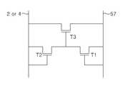
도 1은 정전기 방지회로(electrostatic discharge protection circuit)를 구비한 액정표시패턴의 박막 트랜지스터 어레이 기판을 나타내는 평면도이다.1 is a plan view illustrating a thin film transistor array substrate of a liquid crystal display pattern having an electrostatic discharge protection circuit.
도 1에 박막 트랜지스터 어레이 기판의 표시영역(P1)에는 서로 교차되게 형성된 게이트 라인(2) 및 데이터 라인(4), 게이트 라인(2) 및 데이터 라인(4)의 교차영역에 형성된 박막 트랜지스터(6), 박막 트랜지스터(6)와 접속된 화소전극(18)을 포함한다.In the display area P1 of the thin film transistor array substrate of FIG. 1, the
박막 트랜지스터 어레이 기판의 비표시영역(P2)에는 게이트 라인(2)과 접속되어 게이트 라인에 게이트 전압을 공급하는 게이트 패드(3), 데이터 라인(4)과 접속되어 데이터 라인(4)에 데이터 전압을 공급하는 데이터 패드(5), 게이트 라인(2) 과 공통라인(57) 사이 및 데이터 라인(4)과 공통라인(57) 사이에 형성된 정전기 방지회로(60)를 포함한다. 공통라인(57)은 공통패드(55)와 접속되어 공통패드(55)로부터 기준전압이 공급된다. 한편, 정전기 방지회로(60)는 공통라인(57) 대신 접지(grond) 전극과 연결될 수도 있다.]A
도 2는 도 1의 정전기 방지회로(60)를 상세히 나타내는 회로도이다.FIG. 2 is a circuit diagram illustrating the
도 2에 도시된 정전기 방지회로(60)는 공통라인(또는 접지전극)과 게이트 라인(2) 사이 또는 공통라인(또는 접지전극)과 데이터 라인(4) 사이에 형성된다. 도 2에서는 게이트 라인(2)과 공통라인(57) 사이에 형성된 경우를 나타내었다.The
정전기 방지회로(60)는 공통라인(57)과 데이터 라인(4) 사이에 접속된 제1 내지 제3 트랜지스터(T1 내지 T3)로 구성되어 있다.The
제1 트랜지스터(T1)는 공통라인(57)에 문턱전압(Vth) 이상이 인가되면 턴-온되어 제3 트랜지스터(T3)를 턴온시킴으로써 공통라인(57)으로부터의 전류가 제3 트랜지스터(T3)를 통해 게이트 라인(2)쪽으로 방전되게 한다. 제2 트랜지스터(T2)는 데이터 라인(4)에 문턱전압(Vth) 이상이 인가되면 턴-온되어 제3 트랜지스터(T3)를 턴-온시킴으로써 데이터 라인(4)으로부터의 전류가 제3 트랜지스터(T3)를 통해 공통라인(57)으로 방전되게 된다. 게이트 라인(2)과 공통라인(57) 또한 동일한 원리에 의해 구동된다.When the threshold voltage Vth or more is applied to the
도 3은 도 1에 도시된 정전기 방지회로의 트랜지스터들의 I-V곡선(curve)를 나타내는 도면이다.3 is a diagram illustrating an I-V curve of transistors of the antistatic circuit illustrated in FIG. 1.
도 3를 참조하면, 종래의 정전기 방지회로(60)를 구성하는 제1 내지 제3 트랜지스터(T1 내지 T3)들의 문턱전압(Vth)은 1~2V 정도임에 비하여 데이터 전압(또는 액정구동전압)은 10V 내외이다. 이에 따라, 제1 내지 제3 트랜지스터(T1 내지 T3)에 2Vth 정도의 전압 정도만 공급되면 제1 내지 제3 트랜지스터(T1 내지 T3)가 턴-온 되게 된다.Referring to FIG. 3, the threshold voltages Vth of the first to third transistors T1 to T3 constituting the conventional
그 결과, 통상 액정을 구동하여 화상을 구현하는 경우, 데이터 전압 등이 정전기 방지회로(60)로 소실됨에 따라 액정구동전압이 증가되어 소비전력이 증가되는 문제가 발생된다.As a result, when the image is typically driven by driving the liquid crystal, as the data voltage and the like are lost to the
따라서, 본 발명의 목적은 소비전력을 절감할 수 있는 액정표시장치를 제공함에 있다.Accordingly, an object of the present invention is to provide a liquid crystal display device which can reduce power consumption.
상기 목적을 달성하기 위하여, 본 발명에 따른 액정표시장치는 게이트 라인 및 데이터 라인에 의해 정의되는 액정셀들이 매트릭스 형태로 배열된 액정표시패널과; 상기 액정표시패널에 내장되며 상기 게이트 라인 및 데이터 라인 중 어느 하나와 접속된 정전기 방지회로와; 상기 게이트 라인에 공급되는 제1 게이트 전압과 동일한 전압을 상기 정전기 방지회로에 공급하는 제1 전압공급라인과; 상기 게이트 라인에 공급되는 제2 게이트 전압과 동일한 전압을 상기 정전기 방지회로에 공급하는 제2 전압공급라인을 구비한다.In order to achieve the above object, the liquid crystal display device according to the present invention includes a liquid crystal display panel in which the liquid crystal cells defined by the gate line and the data line are arranged in a matrix form; An antistatic circuit embedded in the liquid crystal display panel and connected to any one of the gate line and the data line; A first voltage supply line configured to supply a voltage equal to the first gate voltage supplied to the gate line to the antistatic circuit; And a second voltage supply line configured to supply a voltage equal to the second gate voltage supplied to the gate line to the antistatic circuit.
상기 정전기 방지회로는 상기 게이트 라인 및 데이터 라인 중 어느 하나와 연결됨과 아울러 상기 제1 전압공급라인과 접속된 제1 스위치부와; 상기 게이트 라인 및 데이터 라인 중 어느 하나와 연결됨과 아울러 상기 제1 전압공급라인과 접속된 제2 스위치부를 구비한다.The antistatic circuit includes: a first switch unit connected to any one of the gate line and the data line and connected to the first voltage supply line; And a second switch unit connected to any one of the gate line and the data line and connected to the first voltage supply line.
상기 제1 스위치부는, 상기 게이트 라인 및 데이터 라인 중 어느 하나에 상기 제1 게이트 전압보다 높은 전압이 공급될 때 턴-온 된다.The first switch unit is turned on when a voltage higher than the first gate voltage is supplied to any one of the gate line and the data line.
상기 제2 스위치부는, 제2 전압공급라인에 상기 제2 게이트 전압보다 낮은 전압이 공급될 때 턴-온 된다.The second switch unit is turned on when a voltage lower than the second gate voltage is supplied to a second voltage supply line.
상기 제1 스위치부는, 상기 데이터 라인 및 게이트 라인 중 어느 하나와 접속된 제1 트랜지스터와, 상기 제1 전압공급라인에 접속되며 상기 제1 트랜지스터와 직렬로 연결된 제2 트랜지스터를 구비하고;The first switch unit includes a first transistor connected to one of the data line and the gate line, and a second transistor connected to the first voltage supply line and connected in series with the first transistor;
상기 제2 스위치부는, 상기 데이터 라인 및 게이트 라인 중 어느 하나와 접속된 제3 트랜지스터와, 상기 제2 전압공급라인에 접속되며 상기 제3 트랜지스터와 직렬로 연결된 제4 트랜지스터를 구비한다.The second switch unit includes a third transistor connected to any one of the data line and the gate line, and a fourth transistor connected to the second voltage supply line and connected in series with the third transistor.
상기 제1 게이트 전압은 상기 액정셀의 박막 트랜지스터를 턴-온 시키는 게이트 하이전압이고, 상기 제2 게이트 전압은 상기 박막 트랜지스터를 턴-오프 시키는 게이트 로우전압인 것을 특징으로 한다.The first gate voltage is a gate high voltage for turning on the thin film transistor of the liquid crystal cell, and the second gate voltage is a gate low voltage for turning off the thin film transistor.
상기 목적 외에 본 발명의 다른 목적 및 특징들은 첨부한 도면들을 참조한 실시예에 대한 설명을 통하여 명백하게 드러나게 될 것이다.Other objects and features of the present invention in addition to the above object will become apparent from the description of the embodiments with reference to the accompanying drawings.
이하, 도 4 내지 도 6을 참조하여 본 발명의 바람직한 실시예에 대하여 설명 하기로 한다.Hereinafter, exemplary embodiments of the present invention will be described with reference to FIGS. 4 to 6.
본원발명의 액정표시장치는 액정셀들이 매트릭스 형태로 배열된 액정표시패널과, 액정표시패널에 구동전압을 공급하는 구동회로들을 포함하게 된다. 액정표시패널은 표시영역에 액정셀들이 매트릭스 형태로 배열되고 비표시영역에는 정전기 방지회로 및 패드 등이 형성된다.The liquid crystal display device of the present invention includes a liquid crystal display panel in which liquid crystal cells are arranged in a matrix, and driving circuits for supplying a driving voltage to the liquid crystal display panel. In a liquid crystal display panel, liquid crystal cells are arranged in a matrix in a display area, and an antistatic circuit and a pad are formed in a non-display area.
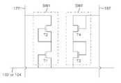
도 4는 본 발명의 실시예에 따른 액정표시장치의 액정표시패널을 나타내는 평면도이다. 특히, 도 4에서는 액정표시패널에서 박막 트랜지스터 어레이 기판을 중심으로 나타내었다.4 is a plan view illustrating a liquid crystal display panel of a liquid crystal display according to an exemplary embodiment of the present invention. In particular, in FIG. 4, the thin film transistor array substrate of the LCD panel is shown.
도 4에 도시된 박막 트랜지스터 어레이 기판의 표시영역(P1)에 형성된 각각의 액정셀들은 서로 교차되게 형성된 게이트 라인(102) 및 데이터 라인(104), 게이트 라인(102) 및 데이터 라인(104)의 교차영역에 형성된 박막 트랜지스터(106), 박막 트랜지스터(106)와 접속된 화소전극(118)을 포함한다.Each of the liquid crystal cells formed in the display area P1 of the thin film transistor array substrate illustrated in FIG. 4 is formed of the
박막 트랜지스터(106)는 게이트 라인(102)으로부터의 게이트 전압에 응답하여 데이터 라인(104)으로부터의 데이터 전압(또는 화소 전압)을 액정셀에 공급한다.The
게이트 라인(102)들에는 박막 트랜지스터(106)를 턴-온 시키기 위한 게이트 하이전압(Vgh)이 순차적으로 공급되고 게이트 하이전압(VGH)이 공급되는 기간을 제외한 나머지 기간에는 게이트 로우전압(Vgl)이 공급된다.The gate lines 102 are sequentially supplied with the gate high voltage Vgh for turning on the
박막 트랜지스터 어레이 기판의 비표시영역(P2)에는 게이트 라인(102)과 접속되어 게이트 라인(102)에 게이트 전압을 공급하는 게이트 패드(103), 데이터 라 인(104)과 접속되어 데이터 라인(104)에 데이터 전압을 공급하는 데이터 패드(105)을 구비한다. 게이트 하이전압(Vgh)이 공급되는 제1 전압공급라인(177)과 게이트 로우전압(Vgl)이 공급되는 제2 전압공급라인(187)과, 게이트 라인(102) 및 데이터 라인(104) 중 어느 하나와 연결된 정전기 방지회로(160)를 구비한다. 정전기 방지회로(160)는 제1 전압공급라인(177) 및 제2 전압공급라인(187)과 각각 접속된다. 또한, 비표시영역(P2)에는 제1 전압공급라인(177)에 게이트 하이전압(Vgh)을 공급하는 제1 전압공급패드(175), 제2 전압공급라인(187)에 게이트 로우전압(Vgl)을 공급하는 제2 전압공급패드(185)가 더 구비된다.In the non-display area P2 of the thin film transistor array substrate, the
도 5는 도 4의 정전기 방지회로(160)를 상세히 나타내는 회로도이다.FIG. 5 is a circuit diagram illustrating the antistatic circuit 160 of FIG. 4 in detail.
도 5에 도시된 정전기 방지회로(160)는 데이터 라인(104)과 제1 전압공급라인(187) 사이에 접속된 제1 스위치부(SW1), 데이터 라인(104)과 제2 전압공급라인(187) 사이에 접속된 제2 스위치부(SW2)로 구성된다.The antistatic circuit 160 shown in FIG. 5 includes a first switch unit SW1, a
제1 스위치부(SW1)는 데이터 라인(104)과 접속된 제1 트랜지스터(T1) 및 제1 전압공급라인(177)에 접속된 제2 트랜지스터(T2)로 구성되고, 제1 및 제2 트랜지스터(T1,T2)는 직렬로 연결된다. 제2 스위치부(SW2)는 데이터 라인(104)과 접속된 제3 트랜지스터(T3) 및 제2 전압공급라인(187)에 접속된 제4 트랜지스터(T4)로 구성되고, 제3 및 제4 트랜지스터(T3,T4)는 직렬로 연결된다.The first switch unit SW1 includes a first transistor T1 connected to the
도 5에서는 데이터 라인(104)과 연결된 정전기 방지회로(160)를 나타내었지만 게이트 라인(102)에 대한 정전기 방지회로 또한 동일한 구조를 나타내게 된다.Although FIG. 5 shows an antistatic circuit 160 connected to the
제1 전압공급라인(187)에는 +20V 정도의 게이트 하이전압(Vgh)이 공급되고, 제2 전압공급라인(177)에는 -5V 정도의 게이트 로우전압(Vgl)이 공급된다.A gate high voltage Vgh of about +20 V is supplied to the first
이러한, 정전기 방지회로(160)의 구동을 살펴보면, 정전기로 인하여 게이트 라인(102)을 통해 게이트 하이전압(Vgh) 보다높은 전압이 인가되면 제1 스위치부(SW1)는 스위칭(턴-온)된다. 이에 따라, 정전기는 데이터 라인(104) 및 제1 스위치부(SW1)을 경유하여 제1 전압공급라인(187)으로 방전될 수 있게 된다. 이와 달리, 제2 전압공급라인(177)에 게이트 로우전압(Vgl) 보다낮은 전압이 인가되면 제2 스위치부(SW2)가 스위칭(턴-온)된다. 이에 따라, 정전기는 제2 전압공급라인(177) 및 제2 스위치부(SW2)를 경유하여 데이터 라인(104)으로 방전될 수 있게 된다.Referring to the driving of the antistatic circuit 160, when a voltage higher than the gate high voltage Vgh is applied through the
그리고, 정전기 방지회로(160)에 게이트 하이전압(Vgh)과 게이트 로운전압(Vgl) 사이의 전압이 공급되는 경우에는 제1 및 제2 스위치부(SW1,SW2)는 턴-오프 상태를 유지하게 된다.When the voltage between the gate high voltage Vgh and the gate blow voltage Vgl is supplied to the antistatic circuit 160, the first and second switch units SW1 and SW2 maintain the turn-off state. do.
이러한 정전기 방지회로의 I-V곡선(curve)을 나타내는 도 6을 참조하면, 통상의 데이터 전압(또는 액정구동전압)은 10V 내외임에 비하여 게이트 하이전압(Vgh)과 게이트 로운전압(Vgl) 사이의 전압은 20V 이상이다. 이에 따라, 화상 구현을 위한 데이터 전압이 공급되더라도 정전기 방지회로(160)로 데이터 전압에 의한 전류가 흐르지 않게 된다. 그 결과, 정전기 방지회로(160)로의 전류 손실을 방지할 수 있게 됨에 따라 액정표시장치 구동을 위한 전체 소비전력을 절감할 수 있게 된다.Referring to FIG. 6, which shows an IV curve of the antistatic circuit, the voltage between the gate high voltage Vgh and the gate low voltage Vgl is about 10V, compared to a typical data voltage (or liquid crystal driving voltage). Is more than 20V. Accordingly, even when a data voltage for image realization is supplied, current due to the data voltage does not flow to the antistatic circuit 160. As a result, it is possible to prevent current loss to the antistatic circuit 160, thereby reducing the overall power consumption for driving the liquid crystal display.
상술한 바와 같이, 본 발명의 실시 예에 따른 액정표시장치는 정전기 방지회로에 게이트 라인에 공급되는 게이트 하이 전압 및 게이트 로우 전압을 공급한다. 이에 따라, 액정 구동을 위한 데이터 전류가 정전기 방지회로로 유입되는 것을 차단할 수 있게 됨으로써 액정 구동을 위한 소비전력을 절감할 수 있게 된다.As described above, the liquid crystal display according to the exemplary embodiment of the present invention supplies the gate high voltage and the gate low voltage supplied to the gate line to the antistatic circuit. Accordingly, the data current for driving the liquid crystal can be blocked from flowing into the antistatic circuit, thereby reducing power consumption for driving the liquid crystal.
이상 설명한 내용을 통해 당업자라면 본 발명의 기술사상을 일탈하지 아니하는 범위에서 다양한 변경 및 수정이 가능함을 알 수 있을 것이다. 예컨대 본 발명의 기술적 사상은 실시예에서 액정표시패널의 전기적 검사를 중심으로 설명되었지만 그와 다른 평판표시장치에 형성된 신호배선들에 대한 전기적 검사에도 동일하게 적용될 수 있을 것이다. 따라서, 본 발명의 기술적 범위는 명세서의 상세한 설명에 기재된 내용으로 한정되는 것이 아니라 특허 청구의 범위에 의해 정하여 져야만 할 것이다.Those skilled in the art will appreciate that various changes and modifications can be made without departing from the technical spirit of the present invention. For example, although the technical concept of the present invention has been described with reference to the electrical inspection of the liquid crystal display panel in the embodiment, the same may also be applied to the electrical inspection of signal wires formed on the other flat panel display device. Therefore, the technical scope of the present invention should not be limited to the contents described in the detailed description of the specification, but should be defined by the claims.
Claims (6)
Translated fromKoreanPriority Applications (2)
| Application Number | Priority Date | Filing Date | Title |
|---|---|---|---|
| KR1020060138722AKR100993420B1 (en) | 2006-12-29 | 2006-12-29 | LCD Display |
| US12/005,618US8947332B2 (en) | 2006-12-29 | 2007-12-28 | Liquid crystal display device having an electrostatic discharge protection circuit |
Applications Claiming Priority (1)
| Application Number | Priority Date | Filing Date | Title |
|---|---|---|---|
| KR1020060138722AKR100993420B1 (en) | 2006-12-29 | 2006-12-29 | LCD Display |
Publications (2)
| Publication Number | Publication Date |
|---|---|
| KR20080062668A KR20080062668A (en) | 2008-07-03 |
| KR100993420B1true KR100993420B1 (en) | 2010-11-09 |
Family
ID=39741247
Family Applications (1)
| Application Number | Title | Priority Date | Filing Date |
|---|---|---|---|
| KR1020060138722AActiveKR100993420B1 (en) | 2006-12-29 | 2006-12-29 | LCD Display |
Country Status (2)
| Country | Link |
|---|---|
| US (1) | US8947332B2 (en) |
| KR (1) | KR100993420B1 (en) |
Families Citing this family (17)
| Publication number | Priority date | Publication date | Assignee | Title |
|---|---|---|---|---|
| TWI334044B (en)* | 2008-04-23 | 2010-12-01 | Au Optronics Corp | Liquid crystal display device having esd protection functionality |
| CN102160103B (en) | 2008-09-19 | 2013-09-11 | 株式会社半导体能源研究所 | Display device |
| EP2172804B1 (en) | 2008-10-03 | 2016-05-11 | Semiconductor Energy Laboratory Co, Ltd. | Display device |
| KR101652693B1 (en) | 2008-10-03 | 2016-09-01 | 가부시키가이샤 한도오따이 에네루기 켄큐쇼 | Display device |
| US8673426B2 (en)* | 2011-06-29 | 2014-03-18 | Semiconductor Energy Laboratory Co., Ltd. | Driver circuit, method of manufacturing the driver circuit, and display device including the driver circuit |
| KR101905779B1 (en) | 2011-10-24 | 2018-10-10 | 삼성디스플레이 주식회사 | Display device |
| US10002968B2 (en) | 2011-12-14 | 2018-06-19 | Semiconductor Energy Laboratory Co., Ltd. | Semiconductor device and display device including the same |
| US9250489B2 (en)* | 2012-11-16 | 2016-02-02 | Shenzhen China Star Optoelectronics Technology Co., Ltd. | LCD panel with anti-electrostatic discharge function and LCD device using same |
| KR102028326B1 (en)* | 2012-12-28 | 2019-11-14 | 엘지디스플레이 주식회사 | Display device |
| KR102105369B1 (en)* | 2013-09-25 | 2020-04-29 | 삼성디스플레이 주식회사 | Mother substrate for a display substrate, array testing method thereof and display substrate |
| KR102134119B1 (en)* | 2013-12-27 | 2020-07-16 | 엘지디스플레이 주식회사 | Liquid crystal display device |
| US9966000B2 (en)* | 2015-01-16 | 2018-05-08 | Apple Inc. | Electro-static discharge and electric overstress protection strategy for micro-chip array on panel |
| CN204667021U (en) | 2015-06-15 | 2015-09-23 | 京东方科技集团股份有限公司 | Array base palte and display device |
| KR102600695B1 (en)* | 2016-12-23 | 2023-11-09 | 엘지디스플레이 주식회사 | Display device |
| CN106950775A (en)* | 2017-05-16 | 2017-07-14 | 京东方科技集团股份有限公司 | A kind of array base palte and display device |
| CN107479283B (en)* | 2017-08-30 | 2020-07-07 | 厦门天马微电子有限公司 | Array substrate, display panel and display device |
| JP2020161678A (en)* | 2019-03-27 | 2020-10-01 | シャープ株式会社 | Imaging panel and board for imaging panel |
Family Cites Families (13)
| Publication number | Priority date | Publication date | Assignee | Title |
|---|---|---|---|---|
| US6587160B2 (en)* | 1997-10-14 | 2003-07-01 | Samsung Electronics Co., Ltd. | Liquid crystal displays |
| JP3396620B2 (en)* | 1998-03-20 | 2003-04-14 | シャープ株式会社 | Active matrix substrate and inspection method thereof |
| KR100386849B1 (en)* | 2001-07-10 | 2003-06-09 | 엘지.필립스 엘시디 주식회사 | Circuit for electro static dischrging of tft-lcd |
| GB0119299D0 (en)* | 2001-08-08 | 2001-10-03 | Koninkl Philips Electronics Nv | Electrostatic discharge protection for pixellated electronic device |
| JP2004246202A (en)* | 2003-02-14 | 2004-09-02 | Koninkl Philips Electronics Nv | Electronic device having an electrostatic discharge protection circuit |
| KR100491560B1 (en)* | 2003-05-06 | 2005-05-27 | 엘지.필립스 엘시디 주식회사 | Method and Apparatus for Testing Liquid Crystal Display Device |
| JP2005115049A (en) | 2003-10-08 | 2005-04-28 | Sharp Corp | Active matrix substrate |
| KR20060086178A (en)* | 2005-01-26 | 2006-07-31 | 삼성전자주식회사 | Liquid crystal display |
| KR101133763B1 (en)* | 2005-02-02 | 2012-04-09 | 삼성전자주식회사 | Driving device of liquid crystal display device and liquid crystal display device including the same |
| TWI270191B (en)* | 2005-09-30 | 2007-01-01 | Innolux Display Corp | Electro static discharge protection circuit |
| JP4586739B2 (en)* | 2006-02-10 | 2010-11-24 | セイコーエプソン株式会社 | Semiconductor integrated circuit and electronic equipment |
| TWI352963B (en)* | 2006-11-08 | 2011-11-21 | Chunghwa Picture Tubes Ltd | Active device array substrate having electrostatic |
| US7795684B2 (en)* | 2006-11-24 | 2010-09-14 | Chunghwa Picture Tubes, Ltd. | Active device array substrate |
- 2006
- 2006-12-29KRKR1020060138722Apatent/KR100993420B1/enactiveActive
- 2007
- 2007-12-28USUS12/005,618patent/US8947332B2/enactiveActive
Also Published As
| Publication number | Publication date |
|---|---|
| US8947332B2 (en) | 2015-02-03 |
| KR20080062668A (en) | 2008-07-03 |
| US20080218652A1 (en) | 2008-09-11 |
Similar Documents
| Publication | Publication Date | Title |
|---|---|---|
| KR100993420B1 (en) | LCD Display | |
| KR101995714B1 (en) | Display device | |
| KR100924222B1 (en) | Electrostatic discharge circuit and liquid crystal display device having same | |
| KR102034112B1 (en) | Liquid crystal display device and method of driving the same | |
| CN100476912C (en) | Semiconductor device, display device, and electronic apparatus | |
| JP5973123B2 (en) | Gate driving device and display device including the same | |
| US8089445B2 (en) | Display apparatus | |
| US12124141B2 (en) | Array substrate, liquid crystal display panel and display device | |
| CN112582382B (en) | Display panel and display device | |
| KR101420444B1 (en) | Liquid crystal display | |
| US8400437B2 (en) | Display device | |
| KR101233145B1 (en) | Liquid crystal display device | |
| US5596342A (en) | Display device having separate short circuit wires for data and gate lines for protection against static discharges | |
| KR102342327B1 (en) | Display device | |
| US20250234650A1 (en) | Array substrate and display apparatus | |
| KR102706388B1 (en) | Display Device Including Static Discharging Unit | |
| US7957110B2 (en) | Display apparatus current discharging method | |
| KR20160092592A (en) | Display substrate | |
| EP1989700B1 (en) | Active-matrix electronic display comprising diode based matrix driving circuit | |
| KR20080084526A (en) | Active Matrix Devices and Flat Panel Displays with Static Protection | |
| KR20190013395A (en) | Gate driving circuit and display device using the same | |
| WO2023155063A1 (en) | Scan circuit and display apparatus | |
| KR20070071705A (en) | LCD Display | |
| US20060018065A1 (en) | Display device and protection circuits thereof | |
| CN120417670A (en) | Display substrate, display panel and display device |
Legal Events
| Date | Code | Title | Description |
|---|---|---|---|
| PA0109 | Patent application | Patent event code:PA01091R01D Comment text:Patent Application Patent event date:20061229 | |
| A201 | Request for examination | ||
| PA0201 | Request for examination | Patent event code:PA02012R01D Patent event date:20080618 Comment text:Request for Examination of Application Patent event code:PA02011R01I Patent event date:20061229 Comment text:Patent Application | |
| PG1501 | Laying open of application | ||
| E902 | Notification of reason for refusal | ||
| PE0902 | Notice of grounds for rejection | Comment text:Notification of reason for refusal Patent event date:20100125 Patent event code:PE09021S01D | |
| E90F | Notification of reason for final refusal | ||
| PE0902 | Notice of grounds for rejection | Comment text:Final Notice of Reason for Refusal Patent event date:20100514 Patent event code:PE09021S02D | |
| E701 | Decision to grant or registration of patent right | ||
| PE0701 | Decision of registration | Patent event code:PE07011S01D Comment text:Decision to Grant Registration Patent event date:20101027 | |
| GRNT | Written decision to grant | ||
| PR0701 | Registration of establishment | Comment text:Registration of Establishment Patent event date:20101103 Patent event code:PR07011E01D | |
| PR1002 | Payment of registration fee | Payment date:20101103 End annual number:3 Start annual number:1 | |
| PG1601 | Publication of registration | ||
| FPAY | Annual fee payment | Payment date:20130930 Year of fee payment:4 | |
| PR1001 | Payment of annual fee | Payment date:20130930 Start annual number:4 End annual number:4 | |
| FPAY | Annual fee payment | Payment date:20141021 Year of fee payment:5 | |
| PR1001 | Payment of annual fee | Payment date:20141021 Start annual number:5 End annual number:5 | |
| FPAY | Annual fee payment | Payment date:20151028 Year of fee payment:6 | |
| PR1001 | Payment of annual fee | Payment date:20151028 Start annual number:6 End annual number:6 | |
| FPAY | Annual fee payment | Payment date:20161012 Year of fee payment:7 | |
| PR1001 | Payment of annual fee | Payment date:20161012 Start annual number:7 End annual number:7 | |
| FPAY | Annual fee payment | Payment date:20171016 Year of fee payment:8 | |
| PR1001 | Payment of annual fee | Payment date:20171016 Start annual number:8 End annual number:8 | |
| FPAY | Annual fee payment | Payment date:20181015 Year of fee payment:9 | |
| PR1001 | Payment of annual fee | Payment date:20181015 Start annual number:9 End annual number:9 | |
| PR1001 | Payment of annual fee | Payment date:20201019 Start annual number:11 End annual number:11 | |
| PR1001 | Payment of annual fee | Payment date:20211101 Start annual number:12 End annual number:12 | |
| PR1001 | Payment of annual fee | Payment date:20221017 Start annual number:13 End annual number:13 | |
| PR1001 | Payment of annual fee | Payment date:20231016 Start annual number:14 End annual number:14 | |
| PR1001 | Payment of annual fee | Payment date:20241015 Start annual number:15 End annual number:15 |