KR100992120B1 - Silicon Crystallization System and Silicon Crystallization Method - Google Patents
Silicon Crystallization System and Silicon Crystallization MethodDownload PDFInfo
- Publication number
- KR100992120B1 KR100992120B1KR1020030015741AKR20030015741AKR100992120B1KR 100992120 B1KR100992120 B1KR 100992120B1KR 1020030015741 AKR1020030015741 AKR 1020030015741AKR 20030015741 AKR20030015741 AKR 20030015741AKR 100992120 B1KR100992120 B1KR 100992120B1
- Authority
- KR
- South Korea
- Prior art keywords
- laser beam
- laser
- chamber
- crystallization process
- sub
- Prior art date
- Legal status (The legal status is an assumption and is not a legal conclusion. Google has not performed a legal analysis and makes no representation as to the accuracy of the status listed.)
- Expired - Lifetime
Links
Images


Classifications
- B—PERFORMING OPERATIONS; TRANSPORTING
- B23—MACHINE TOOLS; METAL-WORKING NOT OTHERWISE PROVIDED FOR
- B23K—SOLDERING OR UNSOLDERING; WELDING; CLADDING OR PLATING BY SOLDERING OR WELDING; CUTTING BY APPLYING HEAT LOCALLY, e.g. FLAME CUTTING; WORKING BY LASER BEAM
- B23K26/00—Working by laser beam, e.g. welding, cutting or boring
- B23K26/02—Positioning or observing the workpiece, e.g. with respect to the point of impact; Aligning, aiming or focusing the laser beam
- B23K26/06—Shaping the laser beam, e.g. by masks or multi-focusing
- B23K26/0604—Shaping the laser beam, e.g. by masks or multi-focusing by a combination of beams
- C—CHEMISTRY; METALLURGY
- C30—CRYSTAL GROWTH
- C30B—SINGLE-CRYSTAL GROWTH; UNIDIRECTIONAL SOLIDIFICATION OF EUTECTIC MATERIAL OR UNIDIRECTIONAL DEMIXING OF EUTECTOID MATERIAL; REFINING BY ZONE-MELTING OF MATERIAL; PRODUCTION OF A HOMOGENEOUS POLYCRYSTALLINE MATERIAL WITH DEFINED STRUCTURE; SINGLE CRYSTALS OR HOMOGENEOUS POLYCRYSTALLINE MATERIAL WITH DEFINED STRUCTURE; AFTER-TREATMENT OF SINGLE CRYSTALS OR A HOMOGENEOUS POLYCRYSTALLINE MATERIAL WITH DEFINED STRUCTURE; APPARATUS THEREFOR
- C30B29/00—Single crystals or homogeneous polycrystalline material with defined structure characterised by the material or by their shape
- C30B29/02—Elements
- C30B29/06—Silicon
- B—PERFORMING OPERATIONS; TRANSPORTING
- B23—MACHINE TOOLS; METAL-WORKING NOT OTHERWISE PROVIDED FOR
- B23K—SOLDERING OR UNSOLDERING; WELDING; CLADDING OR PLATING BY SOLDERING OR WELDING; CUTTING BY APPLYING HEAT LOCALLY, e.g. FLAME CUTTING; WORKING BY LASER BEAM
- B23K26/00—Working by laser beam, e.g. welding, cutting or boring
- B23K26/02—Positioning or observing the workpiece, e.g. with respect to the point of impact; Aligning, aiming or focusing the laser beam
- B23K26/06—Shaping the laser beam, e.g. by masks or multi-focusing
- B23K26/067—Dividing the beam into multiple beams, e.g. multifocusing
- B23K26/0673—Dividing the beam into multiple beams, e.g. multifocusing into independently operating sub-beams, e.g. beam multiplexing to provide laser beams for several stations
- H—ELECTRICITY
- H01—ELECTRIC ELEMENTS
- H01L—SEMICONDUCTOR DEVICES NOT COVERED BY CLASS H10
- H01L21/00—Processes or apparatus adapted for the manufacture or treatment of semiconductor or solid state devices or of parts thereof
- H01L21/02—Manufacture or treatment of semiconductor devices or of parts thereof
- H01L21/02104—Forming layers
- H01L21/02365—Forming inorganic semiconducting materials on a substrate
- H01L21/02367—Substrates
- H01L21/0237—Materials
- H01L21/02422—Non-crystalline insulating materials, e.g. glass, polymers
- H—ELECTRICITY
- H01—ELECTRIC ELEMENTS
- H01L—SEMICONDUCTOR DEVICES NOT COVERED BY CLASS H10
- H01L21/00—Processes or apparatus adapted for the manufacture or treatment of semiconductor or solid state devices or of parts thereof
- H01L21/02—Manufacture or treatment of semiconductor devices or of parts thereof
- H01L21/02104—Forming layers
- H01L21/02365—Forming inorganic semiconducting materials on a substrate
- H01L21/02518—Deposited layers
- H01L21/02521—Materials
- H01L21/02524—Group 14 semiconducting materials
- H01L21/02532—Silicon, silicon germanium, germanium
- H—ELECTRICITY
- H01—ELECTRIC ELEMENTS
- H01L—SEMICONDUCTOR DEVICES NOT COVERED BY CLASS H10
- H01L21/00—Processes or apparatus adapted for the manufacture or treatment of semiconductor or solid state devices or of parts thereof
- H01L21/02—Manufacture or treatment of semiconductor devices or of parts thereof
- H01L21/02104—Forming layers
- H01L21/02365—Forming inorganic semiconducting materials on a substrate
- H01L21/02656—Special treatments
- H01L21/02664—Aftertreatments
- H01L21/02667—Crystallisation or recrystallisation of non-monocrystalline semiconductor materials, e.g. regrowth
- H01L21/02675—Crystallisation or recrystallisation of non-monocrystalline semiconductor materials, e.g. regrowth using laser beams
- H01L21/02678—Beam shaping, e.g. using a mask
- H—ELECTRICITY
- H01—ELECTRIC ELEMENTS
- H01L—SEMICONDUCTOR DEVICES NOT COVERED BY CLASS H10
- H01L21/00—Processes or apparatus adapted for the manufacture or treatment of semiconductor or solid state devices or of parts thereof
- H01L21/02—Manufacture or treatment of semiconductor devices or of parts thereof
- H01L21/02104—Forming layers
- H01L21/02365—Forming inorganic semiconducting materials on a substrate
- H01L21/02656—Special treatments
- H01L21/02664—Aftertreatments
- H01L21/02667—Crystallisation or recrystallisation of non-monocrystalline semiconductor materials, e.g. regrowth
- H01L21/02675—Crystallisation or recrystallisation of non-monocrystalline semiconductor materials, e.g. regrowth using laser beams
- H01L21/02686—Pulsed laser beam
- H—ELECTRICITY
- H01—ELECTRIC ELEMENTS
- H01L—SEMICONDUCTOR DEVICES NOT COVERED BY CLASS H10
- H01L21/00—Processes or apparatus adapted for the manufacture or treatment of semiconductor or solid state devices or of parts thereof
- H01L21/02—Manufacture or treatment of semiconductor devices or of parts thereof
- H01L21/02104—Forming layers
- H01L21/02365—Forming inorganic semiconducting materials on a substrate
- H01L21/02656—Special treatments
- H01L21/02664—Aftertreatments
- H01L21/02667—Crystallisation or recrystallisation of non-monocrystalline semiconductor materials, e.g. regrowth
- H01L21/02691—Scanning of a beam
- H—ELECTRICITY
- H01—ELECTRIC ELEMENTS
- H01L—SEMICONDUCTOR DEVICES NOT COVERED BY CLASS H10
- H01L21/00—Processes or apparatus adapted for the manufacture or treatment of semiconductor or solid state devices or of parts thereof
- H01L21/02—Manufacture or treatment of semiconductor devices or of parts thereof
- H01L21/04—Manufacture or treatment of semiconductor devices or of parts thereof the devices having potential barriers, e.g. a PN junction, depletion layer or carrier concentration layer
- H01L21/18—Manufacture or treatment of semiconductor devices or of parts thereof the devices having potential barriers, e.g. a PN junction, depletion layer or carrier concentration layer the devices having semiconductor bodies comprising elements of Group IV of the Periodic Table or AIIIBV compounds with or without impurities, e.g. doping materials
- H01L21/26—Bombardment with radiation
- H01L21/263—Bombardment with radiation with high-energy radiation
- H01L21/268—Bombardment with radiation with high-energy radiation using electromagnetic radiation, e.g. laser radiation
Landscapes
- Physics & Mathematics (AREA)
- Engineering & Computer Science (AREA)
- Optics & Photonics (AREA)
- Power Engineering (AREA)
- Condensed Matter Physics & Semiconductors (AREA)
- General Physics & Mathematics (AREA)
- Manufacturing & Machinery (AREA)
- Computer Hardware Design (AREA)
- Microelectronics & Electronic Packaging (AREA)
- Chemical & Material Sciences (AREA)
- Crystallography & Structural Chemistry (AREA)
- Plasma & Fusion (AREA)
- Mechanical Engineering (AREA)
- Materials Engineering (AREA)
- High Energy & Nuclear Physics (AREA)
- Electromagnetism (AREA)
- Health & Medical Sciences (AREA)
- Toxicology (AREA)
- Metallurgy (AREA)
- Organic Chemistry (AREA)
- Recrystallisation Techniques (AREA)
Abstract
Translated fromKoreanDescription
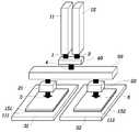
Translated fromKorean도 1은 본 발명의 제1 실시예에 따른 규소 결정화 시스템을 도시한 개략도이고,1 is a schematic diagram showing a silicon crystallization system according to a first embodiment of the present invention,
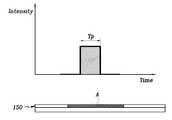
도 2a는 하나의 레이저빔 발생 장치에서 발생한 레이저빔의 펄스 듀레이션 타임에 따른 액상 영역을 도시한 도면이고,FIG. 2A is a diagram illustrating a liquid phase region according to a pulse duration time of a laser beam generated by one laser beam generator.
도 2b는 2개의 레이저빔 발생 장치에서 발생한 레이저빔을 합성한 합성 레이저빔의 펄스 듀레이션 타임에 따른 액상 영역을 도시한 도면이고,FIG. 2B is a view showing a liquid phase region according to a pulse duration time of a synthesized laser beam obtained by synthesizing the laser beams generated by two laser beam generators.
도 3은 도 1에 도시된 레이저빔 분할기의 개략도이고,3 is a schematic diagram of the laser beam splitter shown in FIG. 1,
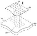
도 4는 레이저를 조사하여 비정질 규소를 다결정 규소로 결정화하는 순차적 측면 결정화 공정을 개략적으로 도시한 도면이고,4 is a view schematically showing a sequential side crystallization process of crystallizing amorphous silicon into polycrystalline silicon by irradiation with a laser,
도 5는 순차적 측면 결정화 공정을 통하여 비정질 규소가 다결정 규소로 결정화되는 과정에서 다결정 규소의 미세 구조를 도시한 도면이고,5 is a view showing the microstructure of polycrystalline silicon in the process of crystallizing amorphous silicon into polycrystalline silicon through a sequential side crystallization process,
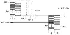
도 6은 순차적 측면 결정화 공정에서 마스크의 이동 위치와 그에 따른 조사 영역을 도시한 도면이고,6 is a view showing a moving position of the mask in the sequential side crystallization process and the corresponding irradiation area,
도 7은 본 발명의 제2 실시예에 따른 규소 결정화 시스템을 도시한 개략도이고,7 is a schematic diagram showing a silicon crystallization system according to a second embodiment of the present invention,
도 8은 도 7에 도시된 레이저빔 분할기의 개략도이고,8 is a schematic diagram of the laser beam splitter shown in FIG. 7,
도 9는 도 9에 도시된 규소 결정화 시스템의 규소 결정화 단계를 도시한 도면이다.9 is a view showing the silicon crystallization step of the silicon crystallization system shown in FIG.
<도면의 주요부분에 대한 부호의 설명><Description of the symbols for the main parts of the drawings>
11 ; 제1 레이저 발생 장치 12 ; 제2 레이저 발생장치11;
21 ; 제1 광계 22 ; 제2 광계21;
31 ; 제1 스테이지 32 ; 제2 스테이지31;
40 ; 레이저빔 합성기 50 ; 레이저빔 분할기40;
210 ; 액상 영역 220 ; 고상 영역210;
300 ; 마스크 310 ; 슬릿 패턴300;
본 발명은 다결정 규소(poly silicon)를 형성하는 시스템 및 다결정 규소를 형성하는 방법에 관한 것으로서, 특히, 박막 트랜지스터 표시판의 다결정 규소층을 형성하는 시스템 및 그 방법에 관한 것이다.The present invention relates to a system for forming polycrystalline silicon and a method for forming polycrystalline silicon, and more particularly, to a system for forming a polycrystalline silicon layer of a thin film transistor array panel and a method thereof.
일반적으로 규소는 결정상태에 따라 비정질 규소(amorphous silicon)와 결정질 규소(crystalline silicon)로 나눌 수 있다. 비정질 규소는 낮은 온도에서 증착하여 박막(thin film)을 형성하는 것이 가능하여, 주로 낮은 용융점을 가지는 유리를 기판으로 사용하는 액정 패널(liquid crystal panel)의 스위칭 소자에 많이 사 용한다.Generally, silicon may be classified into amorphous silicon and crystalline silicon according to the crystal state. Amorphous silicon can be deposited at a low temperature to form a thin film, and is mainly used for switching elements of liquid crystal panels using glass having a low melting point as a substrate.
그러나, 비정질 규소 박막은 낮은 전계 효과 이동도 등의 문제점으로 표시소자의 대면적화에 어려움이 있다. 그래서, 높은 전계 효과 이동도(30㎠/VS)와 고주파 동작특성 및 낮은 누설전류(leakage current)의 전기적 특성을 가진 다결정 규소(poly crystalline silicon)의 응용이 요구되고 있다.However, the amorphous silicon thin film has difficulty in large area of the display device due to problems such as low field effect mobility. Therefore, there is a demand for the application of polycrystalline silicon having high field effect mobility (30
특히, 다결정 규소 박막의 전기적 특성은 그레인(grain)의 크기에 큰 영향을 받는다. 즉, 그레인의 크기가 증가함에 따라 전계 효과 이동도도 따라 증가한다.In particular, the electrical properties of the polycrystalline silicon thin film are greatly influenced by the grain size. That is, as the grain size increases, the field effect mobility also increases.
따라서, 이러한 점을 고려하여 규소를 다결정화 하는 방법이 큰 이슈로 떠오르고 있으며, 최근 들어 에너지원을 레이저로 하여 규소 결정의 측면성장을 유도하여 거대한 다결정 규소를 제조하는 SLS(sequential lateral solidification)(연속적 측면 고상화)기술이 제안되었다.Therefore, the method of polycrystallization of silicon has become a big issue in consideration of this point, and in recent years, the sequential lateral solidification (SLS) (sequential lateral solidification) which induces lateral growth of silicon crystal by using an energy source as a laser to produce huge polycrystalline silicon Lateral solidification techniques have been proposed.
이러한 SLS 기술은 규소 그레인이 액상 규소와 고상 규소의 경계면에서 그 경계면에 대하여 수직 방향으로 성장한다는 사실을 이용한 것으로, 레이저빔(laser beam) 에너지의 크기와 레이저빔의 조사범위의 이동을 광계(optic system) 및 마스크를 이용하여 적절하게 조절하여 규소 그레인을 소정의 길이만큼 측면성장 시킴으로서 비정질 규소층을 결정화시키는 것이다.This SLS technology takes advantage of the fact that silicon grain grows at the interface between liquid silicon and solid silicon in a direction perpendicular to the interface, and shifts the magnitude of the laser beam energy and the shift of the irradiation range of the laser beam. system) and a mask to appropriately control the silicon grains to grow laterally by a predetermined length to crystallize the amorphous silicon layer.
이때, 레이저빔은 슬릿 모양을 가지는 마스크의 투과 영역을 통과하여 비정질 규소를 완전히 녹이고, 비정질 규소층에 슬릿 모양의 액상 영역을 형성한다. 이어서, 액상의 비정질 규소는 냉각되면서 결정화가 이루어지는데, 결정은 레이저가 조사되지 않은 고상 영역과 액상 영역의 경계면에서부터 성장하고, 그 경계면에 대하여 수직 방향으로 성장한다. 그리고, 그레인들의 성장은 액상 영역의 중앙에서 서로 만나면 멈추게 된다. 이러한 공정은 마스크의 슬릿 패턴을 그레인의 성장 방향에 대해 수직으로 이동하면서 진행된다. 그리고, 이러한 공정을 비정질 규소층의 전 영역을 통하여 진행하며, 이때 그레인의 크기는 슬릿 패턴의 폭만큼 성장한다. 비정질 규소층의 전 영역이 결정화 되도록 하기 위해 슬릿 패턴은 마스크 내의 둘 이상의 영역에서 슬릿 패턴의 폭만큼 어긋나게 배치되어 있다. At this time, the laser beam passes through the transmission region of the mask having a slit shape to completely dissolve the amorphous silicon, and forms a slit-shaped liquid region in the amorphous silicon layer. Subsequently, the liquid amorphous silicon is crystallized while cooling, and the crystal grows from the interface between the solid and liquid regions where the laser is not irradiated, and grows in a direction perpendicular to the interface. And the growth of grains stops when they meet each other in the center of the liquid region. This process proceeds by moving the slit pattern of the mask perpendicular to the growth direction of the grain. Then, this process proceeds through the entire region of the amorphous silicon layer, where the grain size grows by the width of the slit pattern. In order to allow the entire region of the amorphous silicon layer to crystallize, the slit patterns are arranged to be shifted by the width of the slit pattern in two or more regions in the mask.
그러나, 이러한 순차적 고상 결정 시스템은 일반적으로 하나의 레이저 발생 장치, 하나의 광계(optic system) 및 하나의 스테이지가 일대일로 대응한다. 이 경우 하나의 레이저 발생 장치에서 발생한 레이저빔은 일반적으로 펄스의 형태이며, 펄스 듀레이션 타임(Pulse duration time)이 짧기 때문에 큰 슬릿 패턴을 가지는 마스크를 이용하는 순차적 고상 결정화 공정을 진행하기 어렵다. 따라서, 이 경우에는 펄스 듀레이션 타임을 연장시켜주는 PDE(Pulse duration extension) 장비가 필수적이므로 비용이 증가된다는 문제점이 있다.However, such a sequential solid-state crystal system generally corresponds one to one laser generating device, one optical system and one stage. In this case, the laser beam generated in one laser generator is generally in the form of a pulse, and since the pulse duration time is short, it is difficult to perform a sequential solid crystallization process using a mask having a large slit pattern. Therefore, in this case, since a PDE (Pulse duration extension) equipment is required to extend the pulse duration time, there is a problem in that the cost is increased.
본 발명은 상기 문제점을 해결하기 위한 것으로서, 양산성을 향상시키고 생산 비용이 절감되는 규소 결정화 시스템 및 규소 결정화 방법을 제공하는 데 목적이 있다.The present invention has been made to solve the above problems, and an object of the present invention is to provide a silicon crystallization system and a silicon crystallization method in which mass production is improved and production cost is reduced.
상기 목적을 달성하기 위한 본 발명의 규소 결정화 시스템은 m은 2 이상의 정수, n은 1 이상의 정수라 할 때, m개의 레이저 발생 장치; 상기 m개의 레이저 발 생 장치에서 발생한 m개의 레이저빔을 합성한 합성 레이저빔을 n개의 서브 레이저빔으로 분할하는 레이저빔 분할기; 상기 분할된 n개의 서브 레이저빔의 각각을 제어하는 n개의 광계; 상기 n개의 광계를 통과한 n개의 서브 레이저빔을 조사함으로써 다결정 규소층으로 결정화되는 비정질 규소층이 증착된 절연 기판을 장착할 수 있는 n개의 스테이지를 포함하는 것이 바람직하다.Silicon crystallization system of the present invention for achieving the above object is m laser generating apparatus when m is an integer of 2 or more, n is an integer of 1 or more; A laser beam splitter for dividing a composite laser beam, which is synthesized with m laser beams generated by the m laser generators, into n sub laser beams; N light systems for controlling each of the divided n sub laser beams; It is preferable to include n stages for mounting an insulating substrate on which an amorphous silicon layer crystallized into a polycrystalline silicon layer is deposited by irradiating n sub laser beams passing through the n optical systems.
또한, 상기 m개의 레이저빔의 각각의 빔펄스가 연속되어 상기 합성 레이저빔의 펄스 듀레이션 타임이 연장되는 것이 바람직하다.In addition, it is preferable that each pulse of the m laser beams is continuous so that the pulse duration time of the composite laser beam is extended.
또한, 상기 레이저빔 분할기는 상기 합성 레이저빔을 동일한 에너지의 n개의 서브 레이저빔으로 분할하는 것이 바람직하다.In addition, the laser beam splitter preferably splits the composite laser beam into n sub laser beams of the same energy.
또한, 상기 합성 레이저빔은 상기 m개의 레이저 발생 장치와 상기 레이저빔 분할기 간의 경로 사이에 위치하는 레이저빔 합성기에 의해 합성되는 것이 바람직하다.Further, the composite laser beam is preferably synthesized by a laser beam synthesizer located between the paths between the m laser generating devices and the laser beam splitter.
또한, 상기 목적을 달성하기 위한 본 발명의 다른 규소 결정화 시스템은 m은 2 이상의 정수, n과 k는 1 이상의 정수라 할 때, m개의 레이저 발생 장치; 상기 m개의 레이저 발생 장치에서 발생한 레이저빔을 합성한 합성 레이저빔을 n개의 서브 레이저빔으로 분할하는 레이저빔 분할기; 상기 서브 레이저빔을 제어하기 위한 광학계를 포함하며 처리 대상물을 로딩할 수 있는 스테이지를 포함하는 k개의 챔버를 포함하고, 상기 k개의 챔버 중 일부의 챔버에서 레이저 조사를 통한 순차적 측면 결정화 공정을 진행하는 동안, 나머지 챔버에서는 처리 대상물을 상기 스테이지 위에 로딩하는 것이 바람직하다.In addition, another silicon crystallization system of the present invention for achieving the above object is m laser generating devices when m is an integer of 2 or more, n and k is an integer of 1 or more; A laser beam splitter for dividing the synthesized laser beam synthesized with the laser beams generated by the m laser generators into n sub laser beams; A k chamber including an optical system for controlling the sub-laser beam and including a stage capable of loading an object to be processed, and performing a sequential lateral crystallization process through laser irradiation in some of the k chambers. During the rest of the chamber, it is desirable to load the treatment object onto the stage.
또한, 상기 m개의 레이저빔의 각각의 빔펄스가 연속되어 상기 합성 레이저빔의 펄스 듀레이션 타임이 연장되는 것이 바람직하다.In addition, it is preferable that each pulse of the m laser beams is continuous so that the pulse duration time of the composite laser beam is extended.
또한, 상기 k개의 챔버 중 일부의 챔버에서 순차적 측면 결정화 공정이 진행되는 시간이 일부 중첩되는 것이 바람직하다.In addition, it is preferable that a part of the k chambers partially overlap a time period during which the sequential side crystallization process proceeds.
또한, 상기 k개의 챔버는 상기 n개의 서브 레이저빔 중 어느 하나가 통과하는 제k 광계; 상기 제k 광계에 대응하는 제k 스테이지를 포함하는 것이 바람직하다.The k chambers may include a k th optical system through which any one of the n sub laser beams passes; It is preferable to include a k-th stage corresponding to the k-th optical system.
또한, 상기 목적을 달성하기 위한 본 발명의 규소 결정화 방법은 2개의 레이저 발생 장치에서 발생한 레이저빔을 합성한 합성 레이저빔을 3개의 서브 레이저빔으로 분할하여 조사하는 각각의 챔버를 제1 챔버, 제2 챔버 및 제3 챔버라 할 때, 상기 제1 챔버에서 비정질 규소층이 증착된 제1 절연 기판을 제1 스테이지 위에 로딩하는 제1 단계; 상기 제1 챔버에서 초기 순차적 측면 결정화 공정을 진행하는 동안, 상기 제2 챔버에서 비정질 규소층이 증착된 제2 절연 기판을 제2 스테이지 위에 로딩하는 제2 단계; 상기 제1 챔버에서 후기 순차적 측면 결정화 공정을 진행하는 동안, 상기 제2 챔버에서 초기 순차적 측면 결정화 공정을 진행하고, 상기 제3 챔버에서 비정질 규소층이 증착된 제3 절연 기판을 제3 스테이지 위에 로딩하는 제3 단계; 상기 제1 챔버에서 비정질 규소층이 증착된 제1 절연 기판을 제1 스테이지 위에 로딩하는 동안, 상기 제2 챔버에서 후기 순차적 측면 결정화 공정을 진행하고, 상기 제3 챔버에서 초기 순차적 측면 결정화 공정을 진행하는 제4 단계; 상기 제1 챔버에서 초기 순차적 측면 결정화 공정을 진행하는 동안, 상기 제2 챔버에 서 비정질 규소층이 증착된 제2 절연 기판을 제2 스테이지 위에 로딩하고, 상기 제3 챔버에서 후기 순차적 측면 결정화 공정을 진행하는 제5 단계를 포함하고, 상기 제3 단계, 제4 단계 및 제5 단계는 반복되는 것이 바람직하다.In addition, the silicon crystallization method of the present invention for achieving the above object is the first chamber, the first chamber, each chamber for irradiating by dividing the synthetic laser beam synthesized with the laser beams generated in the two laser generating apparatus into three sub laser beams; A first step of loading a first insulating substrate, on which a amorphous silicon layer is deposited, in the first chamber, referred to as a second chamber and a third chamber; During the initial sequential lateral crystallization process in the first chamber, a second step of loading a second insulating substrate on which the amorphous silicon layer is deposited in the second chamber onto the second stage; During the later sequential side crystallization process in the first chamber, the initial sequential side crystallization process in the second chamber, and loading a third insulating substrate on which the amorphous silicon layer is deposited in the third chamber on the third stage. Performing a third step; While loading the first insulating substrate on which the amorphous silicon layer is deposited in the first chamber on the first stage, a later sequential side crystallization process is performed in the second chamber, and an initial sequential side crystallization process is performed in the third chamber. A fourth step of doing; During the initial sequential side crystallization process in the first chamber, a second insulating substrate having an amorphous silicon layer deposited thereon is loaded on the second stage, and a later sequential side crystallization process is performed in the third chamber. It includes a fifth step that proceeds, the third step, the fourth step and the fifth step is preferably repeated.
또한, 상기 합성 레이저빔은 레이저빔 분할기에 의해 3개의 서브 레이저빔으로 분할되는 것이 바람직하다.In addition, the composite laser beam is preferably divided into three sub laser beams by a laser beam splitter.
또한, 상기 제3 단계, 제4 단계 및 제5 단계는 상기 3개의 챔버 중 어느 2개의 챔버에서 동시에 순차적 측면 결정화 공정을 진행하는 동안, 상기 3개의 챔버 중 다른 하나의 챔버에서는 비정질 규소층이 증착된 절연 기판을 스테이지 위에 로딩하는 것이 바람직하다.In addition, in the third, fourth and fifth steps, a sequential lateral crystallization process is simultaneously performed in any two chambers of the three chambers, an amorphous silicon layer is deposited in the other one of the three chambers. It is preferable to load the prepared insulating substrate onto the stage.
또한, 상기 제3 단계, 제4 단계 및 제5 단계는 상기 어느 2개의 챔버 중 어느 하나의 챔버에서 초기 순차적 측면 결정화 공정을 진행하는 동안, 상기 어느 2개의 챔버 중 다른 하나의 챔버에서 후기 순차적 측면 결정화 공정을 진행하는 것이 바람직하다.Further, the third, fourth and fifth steps may be performed during the initial sequential side crystallization process in any one of the two chambers, and in the later sequential side in the other one of the two chambers. It is preferable to proceed with the crystallization process.
본 발명의 제1 실시예에 따른 규소 결정화 시스템에 대하여 도면을 참고로 하여 상세하게 설명한다.The silicon crystallization system according to the first embodiment of the present invention will be described in detail with reference to the drawings.
본 발명의 제1 실시예에 따른 규소 결정화 시스템은 m개의 레이저 발생 장치와, m개의 레이저 발생 장치 아래에 배치되는 레이저빔 분할기를 포함한다. 레이저빔 분할기는 m개의 레이저 발생 장치에서 발생한 m개의 레이저빔을 합성한 합성 레이저빔을 동일한 에너지의 n개의 서브 레이저빔으로 분할한다. 레이저빔 분할기의 아래에는 분할된 n개의 서브 레이저빔의 각각을 제어하는 n개의 광계가 위치하고 있다. 그리고, n개의 광계 아래에는 n개의 스테이지가 위치하고 있다. n개의 스테이지는 n개의 광계를 통과한 n개의 서브 레이저빔의 조사에 의해 다결정 규소층으로 결정화되는 비정질 규소층이 증착된 절연 기판을 장착하고 있다. 그리고, 합성 레이저빔은 n개의 레이저 발생 장치와 레이저빔 분할기 사이에 위치하고 있는 레이저빔 합성기에 의해 합성된다. 레이저빔 분할기의 내부에는 n개의 미러가 배치되어 있다. 합성 레이저빔의 에너지를 1이라 할 때, 제1 미러(M1)는 레이저빔 에너지의 1/n만 투과시키고 나머지인 1-(1/n)은 반사한다. 따라서, 제1 미러(M1)에서 반사된 레이저빔 에너지인 1-(1/n)은 제2 미러(M2)로 입사되어 제2 미러(M2)에서 1/n이 반사되고, 1-(2/n)이 투과된다. 그리고, 제2 미러(M2)에서 투과된 1-(2/n)은 제3 미러(M3)로 입사되어 제3 미러(M3)에서 1/n이 반사되고, 1-(3/n)이 투과된다. 여기서, m과 n은 2 이상의 정수이다.The silicon crystallization system according to the first embodiment of the present invention includes m laser generators and a laser beam splitter disposed under the m laser generators. The laser beam splitter divides the synthesized laser beam, which is composed of m laser beams generated by the m laser generators, into n sub laser beams of the same energy. Below the laser beam splitter, n light systems are positioned to control each of the n sub-laser beams. And n stages are located under n optical systems. The n stages are equipped with an insulating substrate on which an amorphous silicon layer is deposited, which is crystallized into a polycrystalline silicon layer by irradiation of n sub laser beams passing through n optical systems. The synthesized laser beam is then synthesized by a laser beam synthesizer located between the n laser generators and the laser beam splitter. N mirrors are arranged inside the laser beam splitter. When the energy of the synthetic laser beam is 1, the first mirror M1 transmits only 1 / n of the laser beam energy and reflects the remaining 1- (1 / n). Therefore, 1- (1 / n), which is the laser beam energy reflected from the first mirror M1, is incident on the second mirror M2, and 1 / n is reflected by the second mirror M2, and 1- (2 / n) is transmitted. Then, 1- (2 / n) transmitted by the second mirror M2 is incident on the third mirror M3, and 1 / n is reflected by the third mirror M3, and 1- (3 / n) is Permeate. Here m and n are integers of 2 or more.
도 1에는 m과 n이 모두 2인 경우의 본 발명의 제1 실시예에 따른 규소 결정화 시스템이 도시되어 있다.1 shows a silicon crystallization system according to a first embodiment of the present invention where both m and n are two.
도 1에 도시된 바와 같이, 제1 실시예에 따른 규소 결정화 시스템은 제1 레이저 발생 장치(11) 및 제2 레이저 발생 장치(12)와, 레이저빔의 형상 및 에너지를 제어하는 제1 광계(21) 및 제2 광계(22), 그리고 제1 광계(21) 및 제2 광계(22)의 각각의 아래에 위치하는 제1 스테이지(31) 및 제2 스테이지(32)를 포함한다.As shown in FIG. 1, the silicon crystallization system according to the first embodiment includes a
제1 레이저 발생 장치(11)에서 발생한 제1 레이저빔(1) 및 제2 레이저 발생 장치(12)에서 발생한 제2 레이저빔(2)은 레이저빔 합성기(40)에 의해 합성된다. 그리고, 레이저빔 합성기(40)는 레이저 발생 장치(11, 12)와 레이저빔 분할기(50) 사 이의 경로상에 위치한다.The
이러한 레이저빔 합성기(40)에 의해 합성된 합성 레이저빔(4)은 하나의 레이저빔 발생 장치에서 발생한 레이저빔과는 달리 펄스 듀레이션 타임(Pulse Duration Time)이 길다.The synthesized
그러나, 도 2a에 도시된 바와 같이, 하나의 레이저빔 발생 장치에서 발생한 레이저빔은 펄스 듀레이션 타임(Pulse Duration Time)이 매우 짧다. 따라서, 레이저빔의 펄스에 의해 비정질 규소층(150)에서 액상화되어 결정화되는 영역(A)이 작다. 그러므로, 큰 슬릿 패턴의 순차적 측면 결정화 공정을 진행하기 어렵다. 따라서 이를 연장시켜주는 PDE(Pulse Duration Extension)장비가 필수적이다.However, as shown in FIG. 2A, the laser beam generated by one laser beam generator has a very short pulse duration time. Therefore, the area A to be liquefied and crystallized in the
그러나, 본 발명의 제1 실시예와 같이 두 개의 레이저빔 발생 장치(11, 12), 두 개의 광계(21, 22) 및 두 개의 스테이지(31, 32)로 이루어진 규소 결정화 시스템은 도 2b에 도시된 바와 같이, 두 개의 레이저빔 발생 장치(11, 12)에서 발생한 두개의 레이저빔(1, 2)을 합치는 과정에서 각각의 레이저빔의 빔 펄스(beam pulse)간에 빔 펄스가 이어질 수 있는 정도의 시차를 두면 펄스 듀레이션 타임(Pulse Duration Time, Tp)이 증가되는 효과를 가져온다. 즉, 2개의 레이저빔(1, 2)의 각각의 빔 펄스가 연속되어 합성 레이저빔(4)의 펄스 듀레이션 타임(Tp)이 연장된다. 따라서, 레이저빔의 펄스에 의해 비정질 규소층(151, 152)에서 액상화되어 결정화되는 영역(B)이 넓어진다. 따라서, PDE없이도 큰 슬릿 패턴의 순차적 측면 결정화 공정이 가능하므로 양산성이 향상된다.However, a silicon crystallization system composed of two
그리고, 레이저빔 합성기(40)의 아래에는 레이저빔 합성기(40)에 의해 합성 된 합성 레이저빔(4)을 2개의 서브 레이저빔(5, 6) 즉, 제1 서브 레이저빔(5) 및 제2 서브 레이저빔(6)으로 분할하는 레이저빔 분할기(50)를 포함한다. Under the
도 3에는 레이저빔 분할기(50)의 개략도가 도시되어 있다.3 shows a schematic diagram of a
도 3에 도시된 바와 같이, 레이저빔 분할기(50)의 내부에는 2개의 미러가 배치되어 있다. 합성 레이저빔(4)의 에너지를 1이라 할 때, 제1 미러(M1)는 합성 레이저빔 에너지의 1/2만 투과시키고 나머지인 1/2은 반사한다. 따라서, 제1 미러(M1)에서 반사된 합성 레이저빔 에너지인 1/2은 제2 미러(M2)로 입사되어 제2 미러(M2)에서 모두 반사된다.As shown in FIG. 3, two mirrors are disposed in the
즉, 제1 미러(M1)는 합성 레이저빔 에너지의 1/2만 투과시키는 렌즈를 사용하고, 제2 미러(M2)는 합성 레이저빔 에너지를 투과시키지 않는 렌즈를 사용한다면 모든 서브 레이저빔(5, 6)의 에너지가 합성 레이저빔 에너지의 1/2로 동일하게 분할된다. 따라서, 펄스 듀레이션 타임(Tp)이 연장되고, 합성 레이저빔 에너지의 1/2로 분할된 두 개의 서브 레이저빔(5, 6)이 제1 광계(21) 및 제2 광계(22)로 각각 입사된다. That is, if the first mirror M1 uses a lens that transmits only half of the synthetic laser beam energy, and the second mirror M2 uses a lens that does not transmit the synthetic laser beam energy, all the
레이저빔 분할기(50)를 통과한 서브 레이저빔(5, 6)의 아래에는 레이저빔의 형상 및 에너지를 제어하는 제1 광계(21)및 제2 광계(22)가 위치하고 있다. 그리고, 제1 광계(21)의 아래에는 제1 스테이지(31)가 위치하고 있고, 제2 광계(22)의 아래에는 제2 스테이지(32)가 위치하고 있다. 이러한 스테이지(31, 32) 위에는 제1 절연 기판(111) 및 제2 절연 기판(112)이 장착되어 있으며, 제1 광계(21) 및 제2 광계(22)를 통과한 서브 레이저빔(5, 6)이 조사되는 비정질 규소층(151, 152)이 제1 절연 기판(111) 및 제2 절연 기판(112) 위에 증착되어 있다.Below the
이러한 비정질 규소층(151, 152)에 서브 레이저빔(5, 6)을 조사하여 다결정 규소층으로 결정화한다. 광계(21, 22)의 아래는 마스크(미도시)가 위치하고 있어 서브 레이저빔은 슬릿 모양을 가지는 마스크의 투과 영역을 통과하여 비정질 규소를 완전히 녹이고, 비정질 규소층에 슬릿 모양의 액상 영역을 형성한 후 고상화시킴으로써 다결정 규소로 결정화하는 순차적 측면 결정화 공정을 진행한다.The amorphous silicon layers 151 and 152 are irradiated with the
이하에서 순차적 측면 결정화 공정에 대해 상세히 설명한다. Hereinafter, the sequential side crystallization process will be described in detail.
도 4는 레이저빔을 조사하여 비정질 규소를 다결정 규소로 결정화하는 순차적 고상 결정 공정을 개략적으로 도시한 개략도이고, 도 5는 순차적 측면 결정화 공정을 통하여 비정질 규소가 다결정 규소로 결정화되는 과정에서 다결정 규소의 미세 구조 및 마스크의 이동을 도시한 도면이다.FIG. 4 is a schematic diagram illustrating a sequential solid phase crystallization process of crystallizing amorphous silicon into polycrystalline silicon by irradiating a laser beam, and FIG. 5 is a diagram of polycrystalline silicon in a process in which amorphous silicon is crystallized into polycrystalline silicon through a sequential side crystallization process. It is a figure which shows the movement of a microstructure and a mask.
도 4에서 보는 바와 같이, 순차적 측면 결정화 공정은 슬릿 패턴(310)으로 형성되어 있는 투과 영역(310)을 가지는 마스크(300)를 통하여 레이저빔을 조사한다. 그리고, 절연 기판(110)의 상부에 형성되어 있는 비정질 규소층(150)을 국부적으로 완전히 녹여 투과 영역(310)에 대응하는 비정질 규소층(150)에 액상 영역(210)을 형성한다. 이때, 다결정 규소의 그레인은 레이저가 조사된 액상 영역(210)과 레이저가 조사되지 않은 고상 영역(220)의 경계면(230)에서 각각 그 경계면에 대하여 수직 방향(도 5 참조, A방향)으로 성장한다. 그레인들의 성장은 액상 영역(210)의 중앙(231)에서 서로 만나면 멈추게 된다.As shown in FIG. 4, the sequential side crystallization process irradiates a laser beam through a
도 5는 슬릿 패턴이 형성되어 있는 마스크를 이용하여 순차적 측면 결정화 공정을 진행하였을 경우 형성되는 다결정 규소의 그레인 구조를 나타낸 것으로 그레인은 A 방향으로 성장하였음을 알 수 있다. FIG. 5 illustrates a grain structure of polycrystalline silicon formed when a sequential side crystallization process is performed using a mask on which a slit pattern is formed, and it can be seen that grain has grown in the A direction.
여기서, 도 4 및 도 5에 도시된 바와 같이, 수평 방향이 긴 형상의 슬릿 패턴(310)을 가지는 마스크를 이용하여 그레인의 크기를 슬릿 패턴의 폭(W)만큼 성장시키기 위해서는 투과 영역(310)을 정의하는 슬릿 패턴이 그레인의 성장 방향(A 방향)으로 슬릿 패턴의 폭(w)만큼 엇갈리도록 배치되어 있는 마스크를 이용한다. 그리고, 이러한 마스크를 이용하여 비정질 규소층에 레이저를 조사하는 결정화 공정을 진행할 때, 슬릿 패턴의 길이 방향(B 방향)으로 마스크(300)의 1/2 크기만큼 마스크(300)를 이동하여 레이저빔을 조사한다. 이때 슬릿 패턴의 폭 방향(A 방향)으로 이웃하는 비정질 규소층에 연속적으로 레이저가 조사되어 그레인의 성장은 슬릿 패턴의 폭 방향(A 방향)으로 연속적으로 이루어진다. 따라서, 슬릿 패턴의 폭(w) 크기의 그레인이 연속적으로 성장된다.4 and 5, in order to grow the grain size by the width W of the slit pattern using a mask having a
이 경우 레이저빔을 한번 조사하는 단위 공정을 샷(Shot)이라 한다. 도 5에 도시된 바와 같이, 제1 차 샷을 진행한 후 마스크를 마스크 가로 길이의 반만큼 이동하여 제2 차 샷을 진행함으로써 마스크에 해당되는 크기의 비정질 규소층이 모두 결정화된다.In this case, a unit process of irradiating a laser beam once is called a shot. As shown in FIG. 5, the amorphous silicon layer having a size corresponding to the mask is crystallized by moving the mask by half of the mask width after the first shot and proceeding the second shot.
그리고, 이러한 샷을 반복해서 진행하며 레이저빔과 마스크(300)를 슬릿 패턴의 길이 방향(B 방향)으로 수평 이동하는 것을 스캐닝이라 한다. 그리고, 이러한 수평 방향으로의 스캐닝의 마지막 지점에서 수직방향으로 레이저빔을 이동하는 것을 스텝핑이라 한다. 이러한 스텝핑 후에 B 방향의 반대 방향으로 스캐닝을 다시 진행한다. 이러한 공정을 반복함으로써 비정질 규소층의 모든 부분이 균일하게 결정화된다.In addition, the laser beam and the
도 6은 순차적 측면 결정화 공정에서 마스크의 이동 과정을 도시한 도면이다.6 is a diagram illustrating a mask movement process in a sequential side crystallization process.
우선, 도 6에서 보는 바와 같이, 다결정 규소용 마스크(300)는 투과 영역(310)을 정의하는 슬릿 패턴들로 이루어진 제1 및 제2 슬릿 영역(G, H)을 가진다. 이때, 제1 및 제2 슬릿 영역(G, H)에 형성되어 있는 슬릿 패턴(310)들은 모두 가로 방향이 긴 형상이며, 각 영역(G, H)에서 동일한 간격을 두고 세로 방향으로 배열되어 있으며, 두 영역(G, H)의 슬릿 패턴(310)은 서로 일정한 간격만큼 어긋나게 배치되어 있다.First, as shown in FIG. 6, the
이러한 마스크를 이용한 순차적 측면 결정화 공정에서는, 도 6에서 보는 바와 같이 제1 차 샷(shot) 공정을 진행할 때, 마스크(300)를 제1 차 샷의 마스크 위치로 이동하여 레이저빔을 조사한다. 이어, 제2 차 샷(shot) 공정을 진행할 때, 마스크(300)를 제2 차 샷의 마스크 위치로 이동하여 레이저빔을 조사한다. 이 때, 제1 차 샷의 마스크의 제2 슬릿 영역(H)과 제2 차 샷의 마스크의 제1 슬릿 영역(G)이 중첩되도록 마스크(300)를 마스크 가로 크기의 반만큼 이동한다.In the sequential side crystallization process using the mask, as shown in FIG. 6, when the first shot process is performed, the
이렇게 여러 차례의 샷을 반복하며 오른쪽 방향으로 스캐닝하며 레이저빔을 조사하여 비정질 규소층(150)의 어느 하나의 수평 라인을 다결정 규소층으로 결정화한다. 그리고, 레이저빔의 제1 차 스캐닝의 오른쪽 마지막 지점에서 레이저빔을 아래쪽으로 스텝핑한다. 이러한 레이저빔을 오른쪽에서 왼쪽으로 제2 차 스캐닝하 며 조사한다. 따라서, 제1 차 스캐닝에 의해 다결정 규소층으로 결정화된 수평 라인에 인접한 다른 하나의 수평 라인을 다결정 규소층으로 결정화한다. 이러한 공정을 반복함으로써 모든 수평 라인이 다결정 규소층으로 결정화되어 모든 비정질 규소층(150)이 결정화된다.The shot is repeated several times, scanning in the right direction, and irradiating a laser beam to crystallize any one horizontal line of the
본 발명의 제2 실시예에 따른 규소 결정화 시스템 및 규소 결정화 방법이 도 7 및 도 8에 도시되어 있다. 여기서, 앞서 도시된 도면에서와 동일한 참조부호는 동일한 기능을 하는 동일한 부재를 가리킨다.Silicon crystallization system and silicon crystallization method according to a second embodiment of the present invention is shown in Figs. Here, the same reference numerals as in the above-described drawings indicate the same members having the same function.
m은 2 이상의 정수, n과 k는 1 이상의 정수라 할 때, 본 발명의 제2 실시예에 따른 규소 결정화 시스템은 m개의 레이저 발생 장치와, m개의 레이저 발생 장치에서 발생한 레이저빔을 합성한 합성 레이저빔을 n개의 서브 레이저빔으로 분할하는 레이저빔 분할기와, 서브 레이저빔을 제어하기 위한 광학계를 포함하며 처리 대상물을 로딩할 수 있는 스테이지를 포함하는 k개의 챔버를 포함한다. 그리고, k개의 챔버 중 일부의 챔버에서 레이저 조사를 통한 순차적 측면 결정화 공정을 진행하는 동안, 나머지 챔버에서는 처리 대상물을 상기 스테이지 위에 로딩한다. 그리고, m개의 레이저빔의 각각의 빔펄스가 연속되어 상기 합성 레이저빔의 펄스 듀레이션 타임이 연장된다. 그리고, k개의 챔버 중 일부의 챔버에서 순차적 측면 결정화 공정이 진행되는 시간이 일부 중첩된다. k개의 챔버는 상기 n개의 서브 레이저빔 중 어느 하나가 통과하는 제k 광계와, 제k 광계에 대응하는 제k 스테이지를 포함한다.When m is an integer of 2 or more, and n and k are an integer of 1 or more, the silicon crystallization system according to the second embodiment of the present invention is a synthetic laser obtained by synthesizing m laser generators and laser beams generated by m laser generators. A laser beam splitter for dividing the beam into n sub laser beams, and k chambers including an optical system for controlling the sub laser beam, and a stage capable of loading an object to be processed. Then, while the sequential side crystallization process through laser irradiation is performed in some of the k chambers, the remaining chamber is loaded with the object on the stage. Each pulse of the m laser beams is successively extended to extend the pulse duration time of the composite laser beam. In addition, the time at which the sequential side crystallization process proceeds in some of the k chambers partially overlaps. The k chambers include a kth optical system through which one of the n sub laser beams passes, and a kth stage corresponding to the kth optical system.
도 7에는 m이 2이고, n 및 k가 3인 경우의 본 발명의 제2 실시예에 따른 규 소 결정화 시스템이 도시되어 있다. 도 7에 도시된 바와 같이, 제2 실시예에 따른 규소 결정화 시스템은 2개의 레이저 발생 장치(11, 12)와, 2개의 레이저 발생 장치(11, 12)에 의해 발생한 레이저빔이 통과하는 레이저빔 분할기(50) 및 레이저빔 분할기(50)에 의해 분할된 3개의 서브 레이저빔(5, 6, 7)의 각각을 제어하는 3개의 챔버(60, 70, 80)를 포함한다.FIG. 7 shows a silicon crystallization system according to a second embodiment of the present invention when m is 2 and n and k are 3. FIG. As shown in FIG. 7, the silicon crystallization system according to the second embodiment includes two
제1 레이저 발생 장치(11)에서 발생한 제1 레이저빔(1) 및 제2 레이저 발생 장치(12)에서 발생한 제2 레이저빔(2)은 레이저빔 합성기(40)에 의해 합성된다. 그리고, 레이저빔 합성기(40)는 레이저 발생 장치(11, 12)와 레이저빔 분할기(50) 사이에 위치한다.The
이러한 레이저빔 합성기(40)에 의해 합성된 합성 레이저빔(4)은 하나의 레이저빔 발생 장치에서 발생한 레이저빔과는 달리 펄스 듀레이션 타임(Pulse Duration Time)이 길다.The synthesized
두 개의 레이저빔 발생 장치(11, 12)에서 발생한 두개의 레이저빔(1, 2)을 합치는 과정에서 각각의 레이저빔의 빔 펄스(beam pulse)간에 빔 펄스가 이어질 수 있는 정도의 시차를 두면 펄스 듀레이션 타임(Pulse Duration Time, Tp)이 증가되는 효과를 가져온다. 즉, 2개의 레이저빔(1, 2)의 각각의 빔 펄스가 연속되어 합성 레이저빔(4)의 펄스 듀레이션 타임(Tp)이 연장된다. 따라서, 레이저빔의 펄스에 의해 비정질 규소층(151, 152, 153)에서 액상화되어 결정화되는 영역(B)이 넓어진다.When the two
레이저빔 분할기(50)는 레이저빔 합성기(40)에 의해 합성된 합성 레이저빔(4)을 3개의 서브 레이저빔(5, 6, 7)으로 분할한다. The
도 8에는 레이저빔 분할기(50)의 개략도가 도시되어 있다.8 shows a schematic diagram of a
도 8에 도시된 바와 같이, 레이저빔 분할기의 내부에는 3개의 미러가 배치되어 있다. 합성 레이저빔(4)의 에너지를 1이라 할 때, 제1 미러(M1)는 레이저빔 에너지의 1/3만 투과시키고 나머지인 2/3는 반사한다. 제1 미러(M1)에서 투과된 레이저빔 이 제1 서브 레이저빔(5)이다. 따라서, 제1 미러(M1)에서 반사된 레이저빔 에너지인 2/3는 제2 미러(M2)로 입사되어 제2 미러(M2)에서 1/3이 반사되고, 1/3이 투과된다. 제2 미러(M1)에서 반사된 레이저빔이 제2 서브 레이저빔(6)이다. 그리고, 제2 미러(M2)에서 투과된 1/3은 제3 미러(M3)로 입사되어 제3 미러(M3)에서 전부 반사된다. 제3 미러(M3)에서 반사된 레이저빔이 제3 서브 레이저빔(7)이다.As shown in FIG. 8, three mirrors are disposed in the laser beam splitter. When the energy of the
즉, 제1 미러(M1)는 레이저빔 에너지의 1/3만 투과시키는 렌즈를 사용하고, 제2 미러(M2)는 레이저빔 에너지의 1/3만 투과시키는 렌즈를 사용하고, 제3 미러(M3)는 레이저빔 에너지의 1/3만 반사시키는 렌즈를 사용한다면 모든 서브 레이저빔(2)의 에너지가 전제 레이저빔 에너지의 1/3로 동일하게 분할된다. That is, the first mirror M1 uses a lens that transmits only one third of the laser beam energy, and the second mirror M2 uses a lens that transmits only one third of the laser beam energy, and the third mirror ( If M3) uses a lens that reflects only one third of the laser beam energy, the energy of all the
따라서, 펄스 듀레이션 타임(Tp)이 연장되고, 합성 레이저빔 에너지의 1/3로 분할된 3개의 서브 레이저빔(5, 6, 7)이 제1 광계(21), 제2 광계(22) 및 제3 광계(23)로 각각 입사된다.Therefore, the pulse duration time Tp is extended, and the three
3개의 챔버(50, 60, 70)는 3개의 서브 레이저빔 중 제1 서브 레이저빔(5)이 통과하는 제1 광계(21) 및 제1 광계(21) 아래에 위치하는 제1 스테이지(31)를 포함하는 제1 챔버(60)를 포함한다. 그리고, 제2 서브 레이저빔(6)이 통과하는 제2 광계(22) 및 제2 광계(22) 아래에 위치하는 제2 스테이지(32)를 포함하는 제2 챔버(70)를 포함한다. 그리고, 제3 서브 레이저빔(7)이 통과하는 제3 광계(23) 및 제3 광계(23) 아래에 위치하는 제3 스테이지(33)를 포함하는 제3 챔버(80)를 포함한다.The three
3개의 챔버 중 어느 2개의 챔버에서 동시에 순차적 측면 결정화 공정을 진행하는 동안, 나머지 다른 하나의 챔버에서는 비정질 규소층이 증착된 절연 기판을 스테이지 위에 로딩한다. 즉, 3개의 챔버 중 어느 2개의 챔버에서 순차적 측면 결정화 공정이 진행되는 시간이 일부 중첩된다. 자세히 설명하면, 순차적 측면 결정화 공정을 초기 순차적 측면 결정화 공정과 후기 순차적 측면 결정화 공정으로 나눌 때, 어느 2개의 챔버 중 어느 하나의 챔버에서 초기 순차적 측면 결정화 공정을 진행하는 동안, 어느 2개의 챔버 중 다른 하나의 챔버에서 후기 순차적 측면 결정화 공정을 진행한다.While the sequential side crystallization process is simultaneously performed in any two of the three chambers, the other chamber is loaded with an insulating substrate on which an amorphous silicon layer is deposited on the stage. That is, some of the three chambers overlap in time for the sequential side crystallization process to proceed. In detail, when the sequential side crystallization process is divided into an initial sequential side crystallization process and a late sequential side crystallization process, the other one of the two chambers is different during the initial sequential side crystallization process in any one of the two chambers. The late sequential side crystallization process is carried out in one chamber.
따라서, 스테이지 위에 절연 기판을 로딩하는 시간이 줄어든다. 즉, 3개의 챔버 중 순차적 측면 결정화 공정이 진행하는 동안 레이저빔이 조사되지 않는 스테이지 위에는 절연 기판을 로딩한다. 따라서, 종래와 달리 절연 기판을 로딩하는 시간을 줄일 수 있다. 로딩 시간을 최소화하게 되면 연속적인 순차적 측면 결정화 공정이 가능하게 된다. 종래의 순차적 고상 결정 시스템에서는 광계의 온도 안정화를 위하여 공정 진행 전에 더미 샷(dummy shot)을 조사하였다. 그러나, 연속적인 순차적 측면 결정화 공정이 가능해지면 이러한 더미 샷들은 최초 레이저빔 발생시에만 필요하게 된다. 따라서, 본 발명의 제2 실시예에서는 PDE 설비비용절감 및 양산성 향상이 가능하다. 그리고, 더미 샷을 줄일 수 있으므로 생산단가를 낮출 수 있다.Thus, the time for loading the insulating substrate on the stage is reduced. That is, the insulating substrate is loaded on the stage where the laser beam is not irradiated during the sequential side crystallization process among the three chambers. Therefore, unlike the related art, it is possible to reduce the time for loading the insulating substrate. Minimizing loading time enables a continuous sequential side crystallization process. In the conventional sequential solid-state crystal system, a dummy shot was irradiated before proceeding to stabilize the temperature of the light system. However, if successive sequential side crystallization processes are possible, these dummy shots are only needed upon initial laser beam generation. Therefore, in the second embodiment of the present invention, it is possible to reduce the cost of PDE equipment and improve mass productivity. In addition, since the dummy shot can be reduced, the production cost can be lowered.
한편, 본 발명의 제1 실시예의 규소 결정화 시스템에 챔버 2개를 추가하여 2개의 챔버에서 순차적 측면 결정화 공정을 진행하는 동안 나머지 2개의 챔버에서는 스테이지 위에 절연 기판을 로딩하는 시스템도 가능하다. 이 경우에도 로딩 시간을 줄일 수 있다는 장점이 있다.On the other hand, the addition of two chambers to the silicon crystallization system of the first embodiment of the present invention, while the sequential side crystallization process in the two chambers is possible, the system for loading the insulating substrate on the stage in the remaining two chambers. Even in this case, there is an advantage that the loading time can be reduced.
이러한 본 발명의 제2 실시예에 따른 규소 결정화 시스템에 의한 규소 결정화 방법을 이하에서 상세히 설명한다.The silicon crystallization method by the silicon crystallization system according to the second embodiment of the present invention will be described in detail below.
도 9에는 본 발명의 제2 실시예에 따른 규소 결정화 시스템에 의한 규소 결정화 방법을 나타내었다.9 shows a silicon crystallization method by a silicon crystallization system according to a second embodiment of the present invention.
도 9에 도시된 바와 같이, 우선 제1 챔버(60)에서는 비정질 규소층(151)이 증착된 제1 절연 기판(111)을 제1 스테이지(31) 위에 로딩한다. 이 경우에 제1 챔버(60)는 입구가 열려지며, 제2 챔버(70) 및 제3 챔버(80)는 입구가 닫혀있다. (제1 단계, P1)As shown in FIG. 9, in the
다음으로, 제1 챔버(60)에서 초기 순차적 측면 결정화 공정을 진행하는 동안, 제2 챔버(70)에서는 비정질 규소층(152)이 증착된 제2 절연 기판(112)을 제2 스테이지(32) 위에 로딩한다. 이 경우에 제2 챔버(70)의 입구가 열려지며, 제3 챔버(80)는 여전히 닫혀있다. 따라서, 제1 챔버(60)에 제1 서브 레이저빔(5)이 조사된다.(제2 단계, P2)Next, while the initial sequential lateral crystallization process is performed in the
다음으로, 제1 챔버(60)에서 후기 순차적 측면 결정화 공정을 진행하는 동안, 제2 챔버(70)에서는 초기 순차적 측면 결정화 공정을 진행하고, 제3 챔버(80) 에서는 비정질 규소층(153)이 증착된 제3 절연 기판(113)을 제3 스테이지(33) 위에 로딩한다. 이 경우에 제3 챔버(80)의 입구가 열려지고, 후기 순차적 측면 결정화 공정이 완료된 제1 챔버(60)의 입구가 닫혀진다. 따라서, 제1 챔버(60) 및 제2 챔버(70)에 각각 제1 서브 레이저빔(5) 및 제2 서브 레이저빔(6)이 조사된다. (제3 단계, P3)Next, while the later sequential side crystallization process is performed in the
다음으로, 제1 챔버(60)에서 비정질 규소층(151)이 증착된 제1 절연 기판(111)을 제1 스테이지(31) 위에 로딩하는 동안, 제2 챔버(70)에서는 후기 순차적 측면 결정화 공정을 진행하고, 제3 챔버(80)에서는 초기 순차적 측면 결정화 공정을 진행한다. 이 경우 후기 순차적 측면 결정화 공정이 완료된 제2 챔버(70)의 입구가 닫혀진다. 따라서, 제2 챔버(70) 및 제3 챔버(80)에 각각 제2 서브 레이저빔(6) 및 제3 서브 레이저빔(7)이 조사된다. (제4 단계, P4)Next, while loading the first insulating
다음으로, 제1 챔버(60)에서 초기 순차적 측면 결정화 공정을 진행하는 동안, 제2 챔버(70)에서는 비정질 규소층(152)이 증착된 제2 절연 기판(112)을 제2 스테이지(32) 위에 로딩하고, 제3 챔버(80)에서는 후기 순차적 측면 결정화 공정을 진행한다. 이 경우 후기 순차적 측면 결정화 공정이 완료된 제3 챔버(80)의 입구가 닫혀진다. 따라서, 제1 챔버(60) 및 제3 챔버(80)에 각각 제1 서브 레이저빔(5) 및 제3 서브 레이저빔(7)이 조사된다. (제5 단계, P5)Next, while the initial sequential lateral crystallization process is performed in the
다음으로, 제3 단계, 제4 단계 및 제5 단계가 반복되며 순차적 측면 결정화 공정이 진행되어 로딩 시간이 줄어들게 된다.Next, the third step, the fourth step and the fifth step are repeated and the sequential side crystallization process is performed to reduce the loading time.
본 발명에 따른 규소 결정화 시스템 및 그 방법은 다수개의 레이저 발생 장치에서 발생한 레이저빔을 합성하여 펄스 듀레이션 타임을 증가시킴으로써, 큰 슬릿 패턴을 가지는 마스크를 이용하는 순차적 고상 결정화 공정에 유리하다. The silicon crystallization system and method thereof according to the present invention are advantageous for a sequential solid phase crystallization process using a mask having a large slit pattern by synthesizing a laser beam generated in a plurality of laser generators and increasing the pulse duration time.
또한, 3개의 챔버를 이용하는 경우에는 로딩 시간을 줄일 수 있으므로 양산성 이 향상되며, 레이저빔의 샷을 줄일 수 있기 때문에 생산 단가를 낮출 수 있다는 장점이 있다.In addition, in the case of using three chambers, since the loading time can be reduced, the productivity is improved, and since the shot of the laser beam can be reduced, there is an advantage of lowering the production cost.
Claims (12)
Translated fromKoreanPriority Applications (4)
| Application Number | Priority Date | Filing Date | Title |
|---|---|---|---|
| KR1020030015741AKR100992120B1 (en) | 2003-03-13 | 2003-03-13 | Silicon Crystallization System and Silicon Crystallization Method |
| TW093106776ATW200507114A (en) | 2003-03-13 | 2004-03-12 | System and method of silicon crystallization |
| US10/549,334US20070042575A1 (en) | 2003-03-13 | 2004-03-12 | Crystallization apparatus and method of amophous silicon |
| PCT/KR2004/000520WO2004086489A1 (en) | 2003-03-13 | 2004-03-12 | System and method of silicon crystallization |
Applications Claiming Priority (1)
| Application Number | Priority Date | Filing Date | Title |
|---|---|---|---|
| KR1020030015741AKR100992120B1 (en) | 2003-03-13 | 2003-03-13 | Silicon Crystallization System and Silicon Crystallization Method |
Publications (2)
| Publication Number | Publication Date |
|---|---|
| KR20040080774A KR20040080774A (en) | 2004-09-20 |
| KR100992120B1true KR100992120B1 (en) | 2010-11-04 |
Family
ID=33095548
Family Applications (1)
| Application Number | Title | Priority Date | Filing Date |
|---|---|---|---|
| KR1020030015741AExpired - LifetimeKR100992120B1 (en) | 2003-03-13 | 2003-03-13 | Silicon Crystallization System and Silicon Crystallization Method |
Country Status (4)
| Country | Link |
|---|---|
| US (1) | US20070042575A1 (en) |
| KR (1) | KR100992120B1 (en) |
| TW (1) | TW200507114A (en) |
| WO (1) | WO2004086489A1 (en) |
Cited By (1)
| Publication number | Priority date | Publication date | Assignee | Title |
|---|---|---|---|---|
| KR20210094681A (en)* | 2020-01-21 | 2021-07-30 | 삼성디스플레이 주식회사 | Laser apparatus and manufacturing method of display device using same |
Families Citing this family (5)
| Publication number | Priority date | Publication date | Assignee | Title |
|---|---|---|---|---|
| KR100956339B1 (en)* | 2003-02-25 | 2010-05-06 | 삼성전자주식회사 | Silicon Crystallization System and Silicon Crystallization Method |
| JP2005167084A (en)* | 2003-12-04 | 2005-06-23 | Fujitsu Ltd | Laser crystallization apparatus and laser crystallization method |
| KR20120008345A (en)* | 2010-07-16 | 2012-01-30 | 삼성모바일디스플레이주식회사 | Laser irradiation device |
| KR101817101B1 (en)* | 2011-03-25 | 2018-01-11 | 삼성디스플레이 주식회사 | Selective crystallization method and laser crystallization apparatus for thereof |
| CN103600170B (en)* | 2013-04-28 | 2015-08-26 | 宝山钢铁股份有限公司 | A kind of longitudinal metal plate loading and unloading and cutting method and system thereof |
Citations (1)
| Publication number | Priority date | Publication date | Assignee | Title |
|---|---|---|---|---|
| JP2000012460A (en) | 1998-06-24 | 2000-01-14 | Matsushita Electric Ind Co Ltd | Thin film forming method and thin film forming apparatus |
Family Cites Families (25)
| Publication number | Priority date | Publication date | Assignee | Title |
|---|---|---|---|---|
| US4701591A (en)* | 1983-11-07 | 1987-10-20 | Matsushita Electric Industrial Co., Ltd | Apparatus for processing multiple workpieces utilizing a single laser beam source |
| US4820899A (en)* | 1987-03-03 | 1989-04-11 | Nikon Corporation | Laser beam working system |
| JPH05226275A (en)* | 1992-02-12 | 1993-09-03 | Nippondenso Co Ltd | Laser annealing device |
| JPH07249591A (en)* | 1994-03-14 | 1995-09-26 | Matsushita Electric Ind Co Ltd | Laser annealing method for semiconductor thin film and thin film semiconductor device |
| US6300176B1 (en)* | 1994-07-22 | 2001-10-09 | Semiconductor Energy Laboratory Co., Ltd. | Laser processing method |
| US5488619A (en)* | 1994-10-06 | 1996-01-30 | Trw Inc. | Ultracompact Q-switched microlasers and related method |
| GB9614037D0 (en)* | 1996-07-04 | 1996-09-04 | Secr Defence | An harmonic generator |
| WO2000025322A1 (en)* | 1998-10-27 | 2000-05-04 | Jmar Technology Co. | Shaped source of soft x-ray, extreme ultraviolet and ultraviolet radiation |
| JP2001023918A (en)* | 1999-07-08 | 2001-01-26 | Nec Corp | Semiconductor thin film forming equipment |
| EP1275036B1 (en)* | 2000-01-11 | 2005-10-26 | Electro Scientific Industries, Inc. | Abbe error correction system and method |
| JP2001326190A (en)* | 2000-05-17 | 2001-11-22 | Nec Corp | Method and apparatus for processing thin film |
| US6362919B1 (en)* | 2000-08-22 | 2002-03-26 | Axsun Technologies, Inc. | Laser system with multi-stripe diode chip and integrated beam combiner |
| JP2002141301A (en)* | 2000-11-02 | 2002-05-17 | Mitsubishi Electric Corp | Laser annealing optical system and laser annealing device using the same |
| MY127193A (en)* | 2000-12-26 | 2006-11-30 | Semiconductor Energy Lab | Laser irradiation apparatus and method of laser irradiation |
| WO2002086954A1 (en)* | 2001-04-19 | 2002-10-31 | The Trustee Of Columbia University In The City Of New York | Method and system for providing a single-scan, continuous motion sequential lateral solidification |
| US6791596B2 (en)* | 2001-06-28 | 2004-09-14 | Ricoh Company, Ltd. | Method and apparatus for image forming capable of effectively generating pixel clock pulses |
| TW552645B (en)* | 2001-08-03 | 2003-09-11 | Semiconductor Energy Lab | Laser irradiating device, laser irradiating method and manufacturing method of semiconductor device |
| JP2003059858A (en)* | 2001-08-09 | 2003-02-28 | Sony Corp | Laser annealing apparatus and thin film transistor manufacturing method |
| US6750423B2 (en)* | 2001-10-25 | 2004-06-15 | Semiconductor Energy Laboratory Co., Ltd. | Laser irradiation method, laser irradiation apparatus, and method of manufacturing a semiconductor device |
| US20040097103A1 (en)* | 2001-11-12 | 2004-05-20 | Yutaka Imai | Laser annealing device and thin-film transistor manufacturing method |
| CA2428187C (en)* | 2002-05-08 | 2012-10-02 | National Research Council Of Canada | Method of fabricating sub-micron structures in transparent dielectric materials |
| US6977775B2 (en)* | 2002-05-17 | 2005-12-20 | Sharp Kabushiki Kaisha | Method and apparatus for crystallizing semiconductor with laser beams |
| US20030227602A1 (en)* | 2002-06-07 | 2003-12-11 | Alberto Scarasso | Image laser projector that using a laser source and a digital or analog mask projects an image in particles suspended in the air |
| CN100352005C (en)* | 2002-07-11 | 2007-11-28 | 株式会社液晶先端技术开发中心 | Crystallization apparatus and crystallization method |
| US6816535B2 (en)* | 2002-09-17 | 2004-11-09 | Northrop Grumman Corporation | Co-alignment of time-multiplexed pulsed laser beams to a single reference point |
- 2003
- 2003-03-13KRKR1020030015741Apatent/KR100992120B1/ennot_activeExpired - Lifetime
- 2004
- 2004-03-12WOPCT/KR2004/000520patent/WO2004086489A1/ennot_activeCeased
- 2004-03-12TWTW093106776Apatent/TW200507114A/enunknown
- 2004-03-12USUS10/549,334patent/US20070042575A1/ennot_activeAbandoned
Patent Citations (1)
| Publication number | Priority date | Publication date | Assignee | Title |
|---|---|---|---|---|
| JP2000012460A (en) | 1998-06-24 | 2000-01-14 | Matsushita Electric Ind Co Ltd | Thin film forming method and thin film forming apparatus |
Cited By (2)
| Publication number | Priority date | Publication date | Assignee | Title |
|---|---|---|---|---|
| KR20210094681A (en)* | 2020-01-21 | 2021-07-30 | 삼성디스플레이 주식회사 | Laser apparatus and manufacturing method of display device using same |
| KR102750609B1 (en) | 2020-01-21 | 2025-01-09 | 삼성디스플레이 주식회사 | Laser apparatus and manufacturing method of display device using same |
Also Published As
| Publication number | Publication date |
|---|---|
| WO2004086489A1 (en) | 2004-10-07 |
| WO2004086489A8 (en) | 2006-01-19 |
| US20070042575A1 (en) | 2007-02-22 |
| KR20040080774A (en) | 2004-09-20 |
| TW200507114A (en) | 2005-02-16 |
Similar Documents
| Publication | Publication Date | Title |
|---|---|---|
| JP3860444B2 (en) | Silicon crystallization method and laser annealing equipment | |
| US7164152B2 (en) | Laser-irradiated thin films having variable thickness | |
| JP4263403B2 (en) | Silicon crystallization method | |
| JP4099767B2 (en) | Polycrystalline silicon forming method and mask for laser device for forming polycrystalline silicon | |
| US9087696B2 (en) | Systems and methods for non-periodic pulse partial melt film processing | |
| WO2007022302A2 (en) | High throughput crystallization of thin films | |
| TWI575571B (en) | Non-periodic pulse processing system and method for partially melted film | |
| KR20120101087A (en) | Systems and methods for non-periodic pulse sequential lateral solidification | |
| KR100303138B1 (en) | Method of crystallizing silicon thin film and manufacturing method of thin film transistor using the same | |
| KR100992120B1 (en) | Silicon Crystallization System and Silicon Crystallization Method | |
| US20030148566A1 (en) | Production method for flat panel display | |
| JP2014075562A (en) | Method of manufacturing crystalline semiconductor, and device of manufacturing crystalline semiconductor | |
| KR100708365B1 (en) | Crystallized semiconductor thin film manufacturing method and its manufacturing apparatus | |
| KR100956339B1 (en) | Silicon Crystallization System and Silicon Crystallization Method | |
| KR20150060746A (en) | Method and apparatus for manufacturing crystal semiconductor film | |
| KR101108169B1 (en) | Continuous side crystallization mask and continuous side crystallization apparatus having the same | |
| JP2007221062A (en) | Semiconductor device manufacturing method and manufacturing apparatus | |
| JP2008147429A (en) | Laser annealer and laser anneal method | |
| JP2020181923A (en) | Manufacturing method of semiconductor film | |
| JPH09213651A (en) | Semiconductor thin film manufacturing apparatus and semiconductor thin film manufacturing method | |
| KR100544438B1 (en) | Mask and Crystallization Method Using the Same | |
| KR20080060876A (en) | Mask pattern and crystallization method using the same. | |
| JP2004103782A (en) | Crystal growth method, crystal growth apparatus, beam branching apparatus, and display apparatus | |
| JP2005167007A (en) | Semiconductor thin film manufacturing method and thin film semiconductor device | |
| EP2497105A1 (en) | Systems and methods for non-periodic pulse partial melt film processing |
Legal Events
| Date | Code | Title | Description |
|---|---|---|---|
| PA0109 | Patent application | Patent event code:PA01091R01D Comment text:Patent Application Patent event date:20030313 | |
| PG1501 | Laying open of application | ||
| A201 | Request for examination | ||
| PA0201 | Request for examination | Patent event code:PA02012R01D Patent event date:20080228 Comment text:Request for Examination of Application Patent event code:PA02011R01I Patent event date:20030313 Comment text:Patent Application | |
| E902 | Notification of reason for refusal | ||
| PE0902 | Notice of grounds for rejection | Comment text:Notification of reason for refusal Patent event date:20100226 Patent event code:PE09021S01D | |
| E701 | Decision to grant or registration of patent right | ||
| PE0701 | Decision of registration | Patent event code:PE07011S01D Comment text:Decision to Grant Registration Patent event date:20100903 | |
| GRNT | Written decision to grant | ||
| PR0701 | Registration of establishment | Comment text:Registration of Establishment Patent event date:20101029 Patent event code:PR07011E01D | |
| PR1002 | Payment of registration fee | Payment date:20101029 End annual number:3 Start annual number:1 | |
| PG1601 | Publication of registration | ||
| FPAY | Annual fee payment | Payment date:20130930 Year of fee payment:4 | |
| PR1001 | Payment of annual fee | Payment date:20130930 Start annual number:4 End annual number:4 | |
| FPAY | Annual fee payment | Payment date:20141001 Year of fee payment:5 | |
| PR1001 | Payment of annual fee | Payment date:20141001 Start annual number:5 End annual number:5 | |
| FPAY | Annual fee payment | Payment date:20170928 Year of fee payment:8 | |
| PR1001 | Payment of annual fee | Payment date:20170928 Start annual number:8 End annual number:8 | |
| FPAY | Annual fee payment | Payment date:20181001 Year of fee payment:9 | |
| PR1001 | Payment of annual fee | Payment date:20181001 Start annual number:9 End annual number:9 | |
| PR1001 | Payment of annual fee | Payment date:20201005 Start annual number:11 End annual number:11 | |
| PR1001 | Payment of annual fee | Payment date:20210927 Start annual number:12 End annual number:12 | |
| PC1801 | Expiration of term | Termination date:20230913 Termination category:Expiration of duration |