KR100989166B1 - LCD and its manufacturing method - Google Patents
LCD and its manufacturing methodDownload PDFInfo
- Publication number
- KR100989166B1 KR100989166B1KR1020030058306AKR20030058306AKR100989166B1KR 100989166 B1KR100989166 B1KR 100989166B1KR 1020030058306 AKR1020030058306 AKR 1020030058306AKR 20030058306 AKR20030058306 AKR 20030058306AKR 100989166 B1KR100989166 B1KR 100989166B1
- Authority
- KR
- South Korea
- Prior art keywords
- reflective
- irregularities
- liquid crystal
- crystal display
- display device
- Prior art date
- Legal status (The legal status is an assumption and is not a legal conclusion. Google has not performed a legal analysis and makes no representation as to the accuracy of the status listed.)
- Expired - Fee Related
Links
Images


Classifications
- G—PHYSICS
- G02—OPTICS
- G02F—OPTICAL DEVICES OR ARRANGEMENTS FOR THE CONTROL OF LIGHT BY MODIFICATION OF THE OPTICAL PROPERTIES OF THE MEDIA OF THE ELEMENTS INVOLVED THEREIN; NON-LINEAR OPTICS; FREQUENCY-CHANGING OF LIGHT; OPTICAL LOGIC ELEMENTS; OPTICAL ANALOGUE/DIGITAL CONVERTERS
- G02F1/00—Devices or arrangements for the control of the intensity, colour, phase, polarisation or direction of light arriving from an independent light source, e.g. switching, gating or modulating; Non-linear optics
- G02F1/01—Devices or arrangements for the control of the intensity, colour, phase, polarisation or direction of light arriving from an independent light source, e.g. switching, gating or modulating; Non-linear optics for the control of the intensity, phase, polarisation or colour
- G02F1/13—Devices or arrangements for the control of the intensity, colour, phase, polarisation or direction of light arriving from an independent light source, e.g. switching, gating or modulating; Non-linear optics for the control of the intensity, phase, polarisation or colour based on liquid crystals, e.g. single liquid crystal display cells
- G02F1/133—Constructional arrangements; Operation of liquid crystal cells; Circuit arrangements
- G02F1/1333—Constructional arrangements; Manufacturing methods
- G02F1/1343—Electrodes
- G02F1/134309—Electrodes characterised by their geometrical arrangement
- G—PHYSICS
- G02—OPTICS
- G02F—OPTICAL DEVICES OR ARRANGEMENTS FOR THE CONTROL OF LIGHT BY MODIFICATION OF THE OPTICAL PROPERTIES OF THE MEDIA OF THE ELEMENTS INVOLVED THEREIN; NON-LINEAR OPTICS; FREQUENCY-CHANGING OF LIGHT; OPTICAL LOGIC ELEMENTS; OPTICAL ANALOGUE/DIGITAL CONVERTERS
- G02F1/00—Devices or arrangements for the control of the intensity, colour, phase, polarisation or direction of light arriving from an independent light source, e.g. switching, gating or modulating; Non-linear optics
- G02F1/01—Devices or arrangements for the control of the intensity, colour, phase, polarisation or direction of light arriving from an independent light source, e.g. switching, gating or modulating; Non-linear optics for the control of the intensity, phase, polarisation or colour
- G02F1/13—Devices or arrangements for the control of the intensity, colour, phase, polarisation or direction of light arriving from an independent light source, e.g. switching, gating or modulating; Non-linear optics for the control of the intensity, phase, polarisation or colour based on liquid crystals, e.g. single liquid crystal display cells
- G02F1/133—Constructional arrangements; Operation of liquid crystal cells; Circuit arrangements
- G02F1/1333—Constructional arrangements; Manufacturing methods
- G02F1/1335—Structural association of cells with optical devices, e.g. polarisers or reflectors
- G02F1/133553—Reflecting elements
- G02F1/133555—Transflectors
- G—PHYSICS
- G02—OPTICS
- G02F—OPTICAL DEVICES OR ARRANGEMENTS FOR THE CONTROL OF LIGHT BY MODIFICATION OF THE OPTICAL PROPERTIES OF THE MEDIA OF THE ELEMENTS INVOLVED THEREIN; NON-LINEAR OPTICS; FREQUENCY-CHANGING OF LIGHT; OPTICAL LOGIC ELEMENTS; OPTICAL ANALOGUE/DIGITAL CONVERTERS
- G02F1/00—Devices or arrangements for the control of the intensity, colour, phase, polarisation or direction of light arriving from an independent light source, e.g. switching, gating or modulating; Non-linear optics
- G02F1/01—Devices or arrangements for the control of the intensity, colour, phase, polarisation or direction of light arriving from an independent light source, e.g. switching, gating or modulating; Non-linear optics for the control of the intensity, phase, polarisation or colour
- G02F1/13—Devices or arrangements for the control of the intensity, colour, phase, polarisation or direction of light arriving from an independent light source, e.g. switching, gating or modulating; Non-linear optics for the control of the intensity, phase, polarisation or colour based on liquid crystals, e.g. single liquid crystal display cells
- G02F1/133—Constructional arrangements; Operation of liquid crystal cells; Circuit arrangements
- G02F1/136—Liquid crystal cells structurally associated with a semi-conducting layer or substrate, e.g. cells forming part of an integrated circuit
- G02F1/1362—Active matrix addressed cells
- H—ELECTRICITY
- H10—SEMICONDUCTOR DEVICES; ELECTRIC SOLID-STATE DEVICES NOT OTHERWISE PROVIDED FOR
- H10D—INORGANIC ELECTRIC SEMICONDUCTOR DEVICES
- H10D86/00—Integrated devices formed in or on insulating or conducting substrates, e.g. formed in silicon-on-insulator [SOI] substrates or on stainless steel or glass substrates
- H10D86/40—Integrated devices formed in or on insulating or conducting substrates, e.g. formed in silicon-on-insulator [SOI] substrates or on stainless steel or glass substrates characterised by multiple TFTs
- H10D86/441—Interconnections, e.g. scanning lines
Landscapes
- Physics & Mathematics (AREA)
- Nonlinear Science (AREA)
- Mathematical Physics (AREA)
- Chemical & Material Sciences (AREA)
- Crystallography & Structural Chemistry (AREA)
- General Physics & Mathematics (AREA)
- Optics & Photonics (AREA)
- Liquid Crystal (AREA)
- Geometry (AREA)
- Engineering & Computer Science (AREA)
- Microelectronics & Electronic Packaging (AREA)
Abstract
Translated fromKoreanDescription
Translated fromKorean도 1은 일반적인 액정표시소자의 평면도.1 is a plan view of a general liquid crystal display device.
도 2a 내지 도 2d는 도 1의 Ⅰ-Ⅰ' 선상을 나타낸 액정표시소자의 공정단면도.2A to 2D are cross-sectional views of a liquid crystal display device taken along the line II ′ of FIG. 1.
도 3은 종래 기술에 따른 반사형 액정표시소자의 평면도.3 is a plan view of a reflective liquid crystal display device according to the prior art.
도 4a 내지 도 4e는 도 3의 Ⅱ-Ⅱ' 선상을 나타낸 액정표시소자의 공정단면도.4A to 4E are cross-sectional views of a liquid crystal display device, taken along the line II-II 'of FIG. 3;
도 5는 종래 기술에 의한 반사전극의 반사요철 배치 구조도.5 is a structure of arrangement of reflective irregularities of the reflective electrode according to the prior art;
도 6은 종래 기술에 의한 액정표시소자의 시야각에 따른 반사율을 나타낸 그래프.6 is a graph showing reflectance according to a viewing angle of a liquid crystal display according to the related art.
도 7은 종래 기술에 의한 액정표시소자의 반사각에 따른 반사율을 나타낸 그래프.7 is a graph showing reflectance according to a reflection angle of a liquid crystal display device according to the related art.
도 8은 본 발명에 따른 액정표시소자의 평면도.8 is a plan view of a liquid crystal display device according to the present invention;
도 9는 도 6의 Ⅲ-Ⅲ' 선상을 나타낸 액정표시소자의 단면구조도.FIG. 9 is a cross-sectional structure diagram of a liquid crystal display device on a line III-III ′ of FIG. 6. FIG.
도 10a 내지 도 10d는 본 발명에 따른 액정표시소자의 공정단면도.10A to 10D are cross-sectional views of a liquid crystal display device according to the present invention.
도 11은 본 발명에 의한 반사전극의 반사요철 배치 구조도.11 is a structure of arrangement of reflective irregularities of the reflective electrode according to the present invention;
도 12는 본 발명에 의한 액정표시소자의 시야각에 따른 반사율을 나타낸 그래프.12 is a graph showing the reflectance according to the viewing angle of the liquid crystal display device according to the present invention.
도 13은 본 발명에 의한 액정표시소자의 반사각에 따른 반사율을 나타낸 그래프.13 is a graph showing the reflectance according to the reflection angle of the liquid crystal display device according to the present invention.
도 14의 (a)는 종래 기술에 의한 패널의 반사율 특성을 나타낸 그래프이고, (b)는 본 발명에 의한 패널의 반사율 특성을 나타낸 그래프.(A) is a graph which shows the reflectance characteristic of the panel by a prior art, (b) is a graph which shows the reflectance characteristic of the panel by this invention.
*도면의 주요 부분에 대한 부호설명* Explanation of symbols on the main parts of the drawings
511 : 하부 기판 512 : 게이트 배선511: lower substrate 512: gate wiring
512a : 게이트 전극 513 : 게이트 절연막512a: gate electrode 513: gate insulating film
514 : 반도체층 515 : 데이터 배선514: semiconductor layer 515: data wiring
515a : 소스 전극 515b : 드레인 전극515a:
516 :보호막 517 : 반사전극516: protective film 517: reflective electrode
517a : 반사요철 526 : 포토 레지스트517a: uneven reflection 526: photoresist
526a : 요철패턴 527 : 무기 절연막526a: uneven pattern 527: inorganic insulating film
529 : 포토 마스크 538 : 콘택홀529
본 발명은 액정표시소자에 관한 것으로 특히, 반사 휘도를 확보하기 위한 액정표시소자 및 그 제조방법에 관한 것이다.BACKGROUND OF THE INVENTION 1. Field of the Invention The present invention relates to a liquid crystal display device, and more particularly, to a liquid crystal display device and a method of manufacturing the same for securing reflection luminance.
최근, 계속해서 주목받고 있는 평판표시소자 중 하나인 액정표시소자는 액체의 유동성과 결정의 광학적 성질을 겸비하는 액정에 전계를 가하여 광학적 이방성을 변화시키는 소자로서, 종래 음극선관(Cathod Ray Tube)에 비해 소비전력이 낮고 부피가 작으며 대형화 및 고정세가 가능하여 널리 사용하고 있다.Recently, the liquid crystal display device, one of the flat panel display devices that are attracting attention, is an element that changes the optical anisotropy by applying an electric field to a liquid crystal that combines the liquidity and the optical properties of the crystal, which is applied to a conventional cathode ray tube. Compared with its low power consumption, small volume, large size, and high definition, it is widely used.
이와 같은 액정표시소자는 신호를 선택적으로 인가하기 위한 박막트랜지스터와 화소전극이 구비된 박막트랜지스터 기판과, 색상 구현을 위한 컬러필터층이 구비된 컬러필터 기판과, 상기 두 기판 사이에 봉입된 액정층으로 구성되어 각종 외부신호에 의해 화상을 표시한다.Such a liquid crystal display device includes a thin film transistor substrate having a thin film transistor and a pixel electrode for selectively applying a signal, a color filter substrate having a color filter layer for implementing colors, and a liquid crystal layer enclosed between the two substrates. The image is displayed by various external signals.
이러한 액정표시소자는 백라이트를 광원으로 이용하는 투과형 액정표시소자와, 백라이트를 광원으로 이용하지 않고 외부 자연광을 이용하는 반사형 액정표시소자와, 상기 백라이트 사용으로 인한 전력소모가 큰 투과형 액정표시소자의 단점과 외부 자연광이 어두울 때 사용이 불가능한 반사형 액정표시소자의 단점을 극복하기 위한 반투과형 액정표시소자로 구분될 수 있다.The liquid crystal display device is characterized by a transmissive liquid crystal display device using a backlight as a light source, a reflective liquid crystal display device using external natural light without using the backlight as a light source, and a transmissive liquid crystal display device with high power consumption due to the backlight. It can be classified into a transflective liquid crystal display device for overcoming the disadvantages of the reflective liquid crystal display device that cannot be used when the external natural light is dark.
상기 반투과형 액정표시소자는 단위 화소영역 내에 반사부와 투과부를 동시에 가지므로 필요에 따라 반사형 및 투과형의 양용이 가능하다.Since the transflective liquid crystal display device has a reflecting portion and a transmitting portion at the same time in the unit pixel area, both of the transmissive type and the transmissive type can be used as necessary.
따라서, 액정표시소자에 따라 화소전극은 투과전극 또는 반사전극으로 형성되는데, 투과형 액정표시소자와 반투과형 액정표시소자의 투과부에는 투과전극이 형성되고 반사형 액정표시소자와 반투과형 액정표시소자의 반사부에는 반사전극이 형성된다.Accordingly, the pixel electrode may be formed as a transmissive electrode or a reflective electrode according to the liquid crystal display device. A transmissive electrode is formed in the transmissive portion of the transmissive liquid crystal display device and the transflective liquid crystal display device, and the reflection of the reflective liquid crystal display device and the transflective liquid crystal display device is reflected. The reflection electrode is formed in the portion.
여기서, 투과형 및 반투과형 액정표시소자의 투과전극은 하부기판을 통해 입 사하는 백라이트에 의한 광을 액정층으로 입사시켜 휘도를 밝게 하고, 반사형 및 반투과형 액정표시소자의 반사전극은 외부 자연광이 밝을 때 상부기판을 통해 입사하는 외부 광을 반사시켜 휘도를 밝게 한다.Here, the transmissive electrodes of the transmissive and semi-transmissive liquid crystal display elements emit light from the backlight incident through the lower substrate into the liquid crystal layer to brighten the brightness, and the reflecting electrodes of the reflective and semi-transmissive liquid crystal display elements exhibit external natural light. When it is bright, it reflects the external light incident through the upper substrate to brighten the brightness.
이 때, 반사형 또는 반투과형의 반사전극의 면적을 넓히면 그 만큼 자연광을 많이 받아들일 수 있기 때문에 휘도가 향상된다.At this time, when the area of the reflective or semi-transmissive reflective electrode is enlarged, the natural light can be received as much as it is, so that the luminance is improved.
이하, 반사전극을 가지는 종래의 액정표시소자를 첨부된 도면을 참조하여 설명하면 다음과 같다.Hereinafter, a conventional liquid crystal display having a reflective electrode will be described with reference to the accompanying drawings.
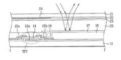
도 1은 일반적인 액정표시소자의 평면도이고, 도 2a 내지 도 2d는 도 1의 Ⅰ-Ⅰ' 선상을 나타낸 액정표시소자의 공정단면도이다.1 is a plan view of a general liquid crystal display device, and FIGS. 2A to 2D are cross-sectional views of a liquid crystal display device showing a line II ′ of FIG. 1.
액정표시소자는 도 1 및 도 2d에서와 같이, 하부기판(11)에 화소영역을 정의하기 위해 게이트 배선(12)과 데이터 배선(15)이 서로 교차하여 배열되고, 상기 게이트 배선(12)과 데이터 배선(15)의 교차 부위에 박막트랜지스터(TFT:Thin Film Transistor)가 형성되며, 상기 박막트랜지스터와 전기적으로 연결되어 각 화소영역에 화소전극(17)이 형성된다.1 and 2D, the
상기 박막트랜지스터는 게이트 전극, 반도체층, 소스/드레인 전극의 적층막으로 구성된다.The thin film transistor includes a stacked film of a gate electrode, a semiconductor layer, and a source / drain electrode.
그리고, 상부기판(21)에는 상기 화소영역을 제외한 부분에서 빛을 차단하기 위한 블랙 매트릭스층(24)과, 각 화소영역에 색상을 구현하기 위한 컬러필터층(22)과, 상기 컬러필터층(22)을 포함한 전면에 공통전극(23)이 형성된다.In addition, the
상기 상,하부 기판(11,21)은 일정한 갭을 갖고 합착되며 그 사이에 액정층(25)이 형성된다.The upper and
상기와 같은 액정표시소자가 반사형 액정표시소자일 경우 상기 화소전극(17)은 고반사율의 금속 일예로 알루미늄, 구리 등으로 형성된다.When the liquid crystal display device as described above is a reflective liquid crystal display device, the
참고로, 투과형 액정표시소자일 경우, 상기 화소전극(17)은 투명한 도전 물질인 ITO 등으로 형성되고, 반사부와 투과부로 정의한 뒤 반사부에 고반사율의 금속을 이용하여 반사전극을 형성하고, 투과부에 상기 반사전극과 연결되는 투과전극을 형성하면 반투과형 액정표시소자가 된다.For reference, in the case of a transmissive liquid crystal display device, the
이와같은 액정표시소자의 제조방법을 설명하면 다음과 같다.Referring to the manufacturing method of such a liquid crystal display device as follows.
먼저, 도 2a에서와 같이, 하부 기판(11) 상에 저저항의 도전성 있는 금속을 스퍼터링 방법으로 증착한 후 포토식각 공정을 통하여 게이트 배선(도 1의 12) 및 게이트 전극(12a)을 형성한다.First, as shown in FIG. 2A, a low resistance conductive metal is deposited on the
다음, 상기 게이트 전극(12a)을 포함한 전면에 게이트 절연막(13)을 형성하고, 상기 게이트 전극(12a) 상부의 게이트 절연막(13) 상에 반도체층(14)을 형성한다.Next, the
그리고, 도 2b에서와 같이, 상기 게이트 절연막(13)을 포함한 전면에 다시 저저항의 금속을 증착하여 포토식각 공정으로써 데이터 배선(도 1의 15) 및 소스/드레인 전극(15a/15b)을 형성한다.As shown in FIG. 2B, a low-resistance metal is again deposited on the entire surface including the
이 때, 데이터 배선(15)은 상기 게이트 배선(12)과 교차되도록 형성하여 단위 화소영역을 정의하고, 상기 소스/드레인 전극(15a/15b)은 상기 반도체층(14) 상에 형성하여 박막트랜지스터를 완성한다.In this case, the
계속하여, 도 2c에서와 같이, 상기 박막트랜지스터를 포함한 전면에 유기 절연물질 또는 무기 절연물질을 소정 두께로 증착하여 보호막(16)을 형성하고, 상기 박막트랜지스터의 드레인 전극(15b)의 소정 부분이 노출되도록 보호막(16)을 제거하여 콘택홀(19)을 형성한다.Subsequently, as shown in FIG. 2C, a
이후, 상기 보호막(16) 상부에 콘택홀(Contact Hole)(19)을 통하여 드레인 전극(15b)과 연결되도록 각 화소영역에 화소전극(17)을 형성한다. 여기서 반사형 액정표시소자일 경우, 화소전극(17)을 고반사율의 금속막인 반사전극으로 한다.Thereafter, a
마지막으로, 도 2d에서와 같이, 블랙 매트릭스층(24), 컬러필터층(24), 및 공통전극(23)이 형성된 상부 기판(21)을 준비한 후, 상부기판(21) 또는 하부기판(11)의 표시영역 가장자리에 씨일 패턴(미도시)을 형성하여 상,하부 기판(11,21)을 대향되도록 합착한 뒤, 두 기판 사이에 액정층(25)을 형성함으로써 소정의 액정표시소자를 완성한다.Finally, as shown in FIG. 2D, after preparing the
이와같이 형성된 반사형 액정표시소자는 상부기판을 통해 입사하는 외부광에 의해 디스플레이된다.The reflective liquid crystal display device thus formed is displayed by external light incident through the upper substrate.
하지만, 반사형 액정표시소자의 경우 일반적으로 광 입사각을 30도 정도로 고려하는데, 이 경우 입사광은 출사각 30도에 대부분 집중되어, 사용자의 주시야각 환경에 해당하는 정면쪽으로는 반사광이 출사되지 못하는 문제점이 있었다.(도 2d참고)However, in the case of the reflective liquid crystal display device, the incident angle of light is generally considered to be about 30 degrees. In this case, the incident light is mostly concentrated at the exit angle of 30 degrees, so that the reflected light cannot be emitted to the front side corresponding to the user's viewing angle. This was (see Figure 2d).
이와 같은 문제점을 해결하고자 사용자의 주시야각 환경인 정면쪽으로 반사광을 출사시키는 기술이 대두되었다.In order to solve this problem, a technology for emitting reflected light toward the front of the user's field of view angle has emerged.
즉, 정면쪽으로 반사광을 출사시키기 위해 상부기판에 산란입자층을 형성하는 방법과, 또는 컬러필터층 내에 산란층을 형성하는 방법과, 반사전극에 반사요철을 형성하는 방법 등이 있다.In other words, there is a method of forming a scattering particle layer on the upper substrate to emit reflected light toward the front, a method of forming a scattering layer in the color filter layer, a method of forming reflective irregularities in the reflective electrode, and the like.
이 중, 반사전극(화소전극)에 반사요철을 이용하는 방법을 구체적으로 살펴보면 다음과 같다.Among them, a method of using reflective irregularities for the reflective electrode (pixel electrode) will be described in detail as follows.
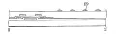
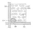
도 3은 종래 기술에 따른 반사형 액정표시소자의 평면도이고, 도 4a 내지 도 4e는 도 3의 Ⅱ-Ⅱ' 선상을 나타낸 액정표시소자의 공정단면도이며, 도 5는 종래 기술에 의한 반사전극의 반사요철 배치 구조도이다.3 is a plan view of a reflection type liquid crystal display device according to the prior art, FIGS. 4A to 4E are cross-sectional views of a liquid crystal display device showing a line II-II 'of FIG. 3, and FIG. 5 is a view of a reflection electrode according to the prior art. It is a structure of arrangement of reflection irregularities.
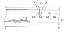
종래 기술에 의한 반사전극은 기존의 편평한 구조가 아니라, 도 4d에서와 같이, 반사전극(117)에 반사요철(117a)을 주어 국부적으로 반사각을 변화시켜서 정면의 반사광량을 확보하는 것이다.The reflective electrode according to the prior art is not a conventional flat structure, but as shown in FIG. 4D, the
상기 요철패턴(129)이 형성된 보호막(116) 위에 반사전극(117)을 형성하여, 상기 하부기판의 보호막(116) 상에 요철패턴(129)이 형성되고, 외부에서 입사하는 광이 반사되어 출사될 때 요철패턴이 형성된 반사전극이 여러 각도로 입사한 빛을 일정한 각도로 결집하여 출사시키는 역할을 한다.The
상기 반사요철(117a)을 형성하는 방법을 구체적으로 살펴보면, 도 4a에서와 같이, 박막트랜지스터(TFT)를 포함한 전면에 보호막(116)을 형성하고, 상기 보호막(116) 상에 포토아크릴 수지(119)를 도포한다.Looking at the method of forming the reflective concave-convex 117a in detail, as shown in Figure 4a, a
다음, 도 4b에서와 같이, 포토식각 공정으로 상기 포토아크릴 수지(119)를 패터닝하여 일정한 간격의 포토아크릴 수지 패턴(119a)을 복수개 형성하고, 도 4c 에서와 같이, 포토아크릴 수지 패턴(119a)을 리플로우(reflow)시켜 반구형의 요철패턴(129)을 형성한다. 상기 요철패턴(129)은 반구형 형태로 소정 간격 이격시켜 형성한다.Next, as shown in FIG. 4B, the
이후, 도 4d에서와 같이, 박막트랜지스터의 드레인 전극(115b)이 노출되도록 상기 보호막(116)을 선택적으로 제거하여 콘택홀(138)을 형성한다.Thereafter, as shown in FIG. 4D, the
상기 콘택홀(138)을 포함한 하부 기판(111) 전면에 반사특성이 우수한 도전성 불투명 금속을 증착하고 패터닝하여 반사전극(117)을 형성한다. 이 때, 상기 요철패턴(129)의 표면을 따라 반사전극(117)에 반사요철(117a)이 형성된다.The
상기 반사요철(117a)은 도 3 및 도 5에서와 같이, 독립된 반구형 형태로 복수개 형성되는데, 반사요철과 반사요철 사이의 거리가 거의 균일하여 시야각에 따른 반사율이 거의 같아 반사광이 대칭적인 특성을 나타낸다.As shown in FIGS. 3 and 5, a plurality of
도 6은 종래 기술에 의한 액정표시소자의 시야각에 따른 반사율을 나타낸 그래프로서, 반사 시야각에 따른 반사율이 거의 같음을 볼 수 있다.6 is a graph showing reflectance according to a viewing angle of a liquid crystal display according to the related art, and it can be seen that the reflectance according to the reflecting viewing angle is about the same.
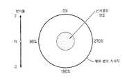
그리고, 도 7은 종래 기술에 의한 액정표시소자의 반사각에 따른 반사율을 나타낸 그래프로서, 대체로 반사각 20도 사이에서 출사각이 집결되어 있음을 알 수 있다. 이는 정면에 대해서 상,하,좌,우 모두에서 동일하게 나타났다.7 is a graph showing reflectance according to the reflection angle of the liquid crystal display according to the related art, and it can be seen that the emission angles are generally collected between the reflection angles of 20 degrees. This was the same for the front, bottom, left and right.
상기와 같은 종래의 액정표시소자 및 그 제조방법은 다음과 같은 문제점이 있다.The conventional liquid crystal display device and its manufacturing method as described above have the following problems.
즉, 반사요철 사이의 거리가 균일하고 그 형태도 동일하여 반사요철의 배치 가 대칭적 구조를 이루어 어느 방향에서나 빛을 반사시키는 반사면의 밀도와 면적이 같아지는데, 이는 반사광을 일정각으로만 출사시키므로 반사율을 증가시키는데 한계가 있었다.That is, the distance between the reflective irregularities is uniform and the shape is the same, so the arrangement of the reflective irregularities forms a symmetrical structure so that the density and the area of the reflective surface reflecting the light in any direction are the same, which emits the reflected light only at a certain angle. As a result, there was a limit to increasing the reflectance.
본 발명은 상기와 같은 문제점을 해결하기 위하여 안출한 것으로, 반사요철의 밀도를 비대칭적으로 조절하여 반사 시야각의 반사율을 증가시켜 반사휘도를 확보하고자 하는 액정표시소자 및 그 제조방법을 제공하는데 그 목적이 있다.The present invention has been made to solve the above problems, to provide a liquid crystal display device and a method of manufacturing the same to secure the reflection brightness by increasing the reflectance of the reflection viewing angle by asymmetrically adjusting the density of the reflection irregularities There is this.
상기와 같은 목적을 달성하기 위한 본 발명의 액정표시소자는 화소영역을 정의하기 위해 서로 수직한 방향으로 형성되는 게이트 배선 및 데이터 배선과, 상기 게이트 배선과 데이터 배선이 교차하는 부분에 형성되는 박막트랜지스터와, 상기 박막트랜지스터를 포함한 전면에 형성된 보호막과, 상기 보호막 상의 상기 화소영역 내에 형성되고, 복수의 원형 요철이 서로 부분적으로 오버랩된 형태를 각각 가지는 반사요철들을 포함하며, 상기 박막트랜지스터와 연결되는 반사전극을 포함한다. 여기서, 상기 반사요철들 간의 거리가 불규칙적으로 되어, 상기 반사요철들은 상기 화소영역 내에서 비대칭적으로 배치되는 것을 특징으로 한다.In order to achieve the above object, a liquid crystal display device according to an embodiment of the present invention includes a gate line and a data line formed in a direction perpendicular to each other to define a pixel region, and a thin film transistor formed at a portion where the gate line and the data line cross. And a protective film formed on the front surface including the thin film transistor, and reflective irregularities formed in the pixel area on the protective film and having a plurality of circular irregularities partially overlapping each other, and connected to the thin film transistor. An electrode. Here, the distance between the reflective irregularities is irregular, the reflective irregularities are characterized in that the asymmetrical arrangement in the pixel area.
또한, 상기와 같은 목적을 달성하기 위한 본 발명의 액정표시소자의 제조방법은 기판 상에 복수개의 배선 및 박막트랜지스터를 형성하는 단계와, 상기 박막트랜지스터를 포함한 전면에 보호막을 형성하는 단계와, 상기 보호막 상에, 복수의 원형 요철이 서로 부분적으로 오버랩된 형태를 가지는 요철패턴을 형성하는 단계와, 상기 보호막 상에, 상기 박막트랜지스터와 전기적으로 연결되고, 상기 요철패턴에 대응하는 반사요철들을 가지는 반사전극을 형성하는 단계를 포함한다. 여기서, 상기 반사요철들은 상기 요철패턴과 같이, 복수의 원형 요철이 서로 부분적으로 오버랩된 형태를 갖고, 상기 반사요철들 간의 거리가 불규칙적으로 되어 비대칭적으로 배치되는 것을 특징으로 한다.In addition, the manufacturing method of the liquid crystal display device of the present invention for achieving the above object comprises the steps of forming a plurality of wiring and a thin film transistor on the substrate, forming a protective film on the entire surface including the thin film transistor, Forming a concave-convex pattern having a form in which a plurality of circular concave-convex portions are partially overlapped with each other on the passivation layer, and a reflection having the concave-convex concave-convex pattern electrically connected to the thin film transistor on the passivation layer and corresponding to the concave-convex pattern Forming an electrode. Here, the reflective irregularities have a form in which a plurality of circular irregularities are partially overlapped with each other, as in the irregular pattern, and the distances between the reflective irregularities are irregular and arranged asymmetrically.
이 때, 상기 반사전극은 상기 요철패턴의 표면을 따라 형성된다.In this case, the reflective electrode is formed along the surface of the uneven pattern.
이러한 본 발명은 반사형 및 반투과형 액정표시소자 모두에 적용 가능한 것으로써, 반사요철이 복수의 원형 요철이 오버랩된 형태를 지니는바, 반사면의 크기와 면적이 증가되고 일방향에 대한 반사광의 휘도가 향상되는 것을 특징으로 한다.The present invention is applicable to both reflective and semi-transmissive liquid crystal display devices, and the reflection irregularities have a form in which a plurality of circular irregularities overlap, so that the size and area of the reflective surface are increased and the luminance of the reflected light in one direction is increased. It is characterized by being improved.
이하, 첨부된 도면을 참조하여 본 발명에 의한 액정표시소자 및 그 제조방법을 살펴보면 다음과 같다.Hereinafter, a liquid crystal display and a manufacturing method thereof according to the present invention will be described with reference to the accompanying drawings.
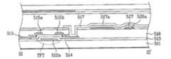
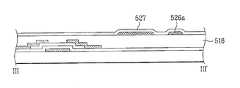
도 8은 본 발명에 따른 액정표시소자의 평면도이고, 도 9은 도 8의 Ⅲ-Ⅲ' 선상을 나타낸 액정표시소자의 단면 구조도이다. 그리고, 도 10a 내지 도 10d는 본 발명에 따른 액정표시소자의 공정단면도이고, 도 11은 본 발명에 의한 반사요철의 배치 구조도이다.FIG. 8 is a plan view of the liquid crystal display device according to the present invention, and FIG. 9 is a cross-sectional structure diagram of the liquid crystal display device shown along the line III-III ′ of FIG. 8. 10A to 10D are cross-sectional views of a liquid crystal display device according to the present invention, and FIG. 11 is a layout diagram of arrangement of reflective irregularities according to the present invention.
도 8 및 도 9에서와 같이, 본 발명에 의한 액정표시소자의 하부 기판(511)은 서로 수직한 방향으로 배열되어 단위 화소영역을 구분짓는 게이트 배선(512) 및 데이터 배선(515)과, 상기 게이트 배선(512)과 데이터 배선(515)의 교차 부위에 형성된 박막트랜지스터(TFT)와, 원형 요철이 일방향으로 부분적으로 오버랩된 형태의 반사요철(517a)을 갖고, 상기 박막트랜지스터와 전기적으로 연결되어 각 화소영역에 형성되는 반사전극(517)이 구비된다.8 and 9, the
이 때, 상기 박막트랜지스터는 상기 게이트 배선에서 분기된 게이트 전극(512a)과, 상기 게이트 전극(512a) 상부에 적층된 게이트 절연막(513)과, 상기 게이트 전극(512a) 상부에 섬(island) 모양으로 형성된 반도체층(514)과, 상기 데이터 배선에서 분기되어 상기 반도체층(514) 상부에 형성된 소스/드레인 전극(515a, 515b)으로 구성된다.In this case, the thin film transistor has a
상기 요철패턴(526a)과 반사전극(517) 사이에는 요철패턴(526a)의 곡률을 제어하고 내화학성 및 내열성이 약한 점을 보완하기 위해 무기 절연막(527)이 더 구성되기도 한다.An inorganic insulating
상기 반사요철(517a)은 반사요철간 거리가 불규칙적이어서 한 화소영역에 대해서 비대칭적인 배치 구조를 가진다.The
이로써, 일방향으로의 빛을 반사시키는 반사면의 면적이 켜져 당해 방향으로의 반사율이 증가하고 또한, 반사요철의 형태가 약간씩 상이해져 반사광의 출사각이 국부적으로 달라짐으로써 사용자의 주사용 환경에 해당하는 정면쪽으로의 반사광도 증가한다.As a result, the area of the reflecting surface reflecting light in one direction is turned on, the reflectance in the direction is increased, and the shape of the reflecting irregularities is slightly different, so that the emission angle of the reflected light is locally changed to correspond to the user's scanning environment. The reflected light toward the front also increases.
각 반사요철의 형태가 다소 상이해지는 이유는 원형 요철이 오버랩되는 면적이 다르거나, 또는 오버랩되는 원형 요철의 개수가 다르기 때문이다.The reason why the shape of each reflective irregularity is slightly different is that the area of overlapping circular irregularities is different or the number of overlapping circular irregularities is different.
도 8에서와 같이 좌우방향으로 복수의 원형 요철이 오버랩되는 반사요철을 가지는 경우 빛을 입사하고 반사하는 반사면의 크기와 면적이 좌우방향으로 증가하므로 결국, 상부기판을 통해 출사하는 반사광은 상하방향으로 증가하게 된다.As shown in FIG. 8, when the plurality of circular irregularities are overlapped in the left and right directions, the size and the area of the reflecting surface incident and reflecting light increase in the left and right directions, so that the reflected light emitted through the upper substrate is vertically To increase.
이와같은 본 발명에 따른 액정표시소자의 제조방법을 설명하면 다음과 같다.Referring to the manufacturing method of the liquid crystal display device according to the present invention as follows.
도 10a에서와 같이, 우선 하부 기판(511) 상에 복수개의 게이트 배선(도 8의 512) 및 게이트 전극(512a)을 형성하고, 상기 게이트 전극(512a)을 포함한 전면에 실리콘질화물(SiNx) 또는 실리콘산화물(SiOx) 등의 무기절연막을 증착하여 게이트 절연막(513)을 형성한다.As shown in FIG. 10A, first, a plurality of
그리고, 상기 게이트 전극(512a) 상부의 게이트 절연막(513)에 비정질 실리 콘(armophous silicon)을 증착하고 섬모양으로 패터닝하여 반도체층(514)을 형성한다. 이때, 도시하지는 않았지만 불순물이온이 주입된 반도체층을 증착하여 오믹콘택층(Ohmic Contact layer)을 형성하기도 한다.In addition, amorphous silicon (armophous silicon) is deposited on the
계속해서, 상기 게이트 배선과 교차하여 화소 영역을 이루도록 복수개의 데이터 배선(도 8의 515)을 형성하고, 이와 동시에 반도체층 양 끝에 소스 전극(515a)과 드레인 전극(515b)을 각각 형성하여 게이트 전극(512a), 게이트 절연막(513), 반도체층(514), 소스/드레인 전극(515a,515b)으로 이루어지는 박막트랜지스터(TFT)를 완성한다.Subsequently, a plurality of data lines (515 in FIG. 8) are formed to intersect the gate lines to form pixel regions, and at the same time,
여기서, 상기 게이트 배선, 게이트 전극, 데이터 배선, 소스/드레인 전극은 크롬(Cr), 몰리브덴(Mo), 알루미늄(Al), 주석(Sn), 구리(Cu)등의 저저항 도전물질을 사용하여 스퍼터링 방법으로 증착한 후 포토식각 공정을 이용하여 패터닝한다.Here, the gate wiring, the gate electrode, the data wiring, and the source / drain electrode are made of low resistance conductive materials such as chromium (Cr), molybdenum (Mo), aluminum (Al), tin (Sn), and copper (Cu). After the deposition by the sputtering method is patterned using a photoetch process.
다음, 상기 박막트랜지스터가 형성된 기판 전면에 보호막(516)을 증착하고, 상기 보호막(516) 상에 포토 레지스트(526)를 도포한다. 이 때, 상기 보호막(516)은 BCB(Benzocyclobutene), 폴리이미드, 아크릴 수지 등의 유기 절연막 또는 SiNx, SiOx 등의 무기 절연막 중 어느 하나로 형성하고 상기 포토 레지스트(526)는 포토 아크릴과 같은 감광특성이 있는 저유전 물질로 한다.Next, a
계속해서, 상기 포토 레지스트(526) 상부에 포토 마스크(529)를 씌우고 광선, 일반적으로 UV 또는 x-선을 조사하여 포토 마스크(529)에 형성된 패턴을 포토 레지스트(526)에 노광시킨 뒤, 현상액을 이용하여 노광된 부분을 현상한다.Subsequently, a
다음, 도 10b에서와 같이, 현상된 포토 레지스트(526)를 리플로우시키는 일 련의 과정을 통해 포토 레지스트를 패터닝하여 요철패턴(526a)을 형성한다.Next, as shown in FIG. 10B, the
이와같이 형성된 요철패턴은 원형 요철이 오버랩되어 다수의 아령 형태, 타원 형태로 다양하게 형성할 수 있으며, 원형 요철이 주시야각 방향에 대한 90도 방향으로 오버랩되도록 한다. 이 때, 원형 요철의 직경은 대체로 5㎛정도로 한다.The concave-convex pattern formed as described above may be variously formed in the form of a plurality of dumbbells and ellipses by overlapping the circular concave-convex, so that the circular concave-convex overlaps in a 90 degree direction with respect to the viewing angle. At this time, the diameter of the circular irregularities is approximately 5 탆.
상기 포토 마스크(529)는 복수의 원이 일방향으로 부분적으로 오버랩된 형태의 광차단막이 형성된 것으로 한다. 이 때, 원들이 오버랩되는 정도나 오버랩되는 개수는 무관하나, 원들 각각을 섬 형태로 독립적으로 배치하고 원들 사이의 거리만 불규칙하게 형성할 경우 모아레 현상이 발생하므로 주의한다.The
이후, 도 10c에서와 같이, 상기 요철패턴(526a)을 포함한 전면에 요철패턴과 동일한 재료를 0.8㎛정도의 두께로 도포하여 무기 절연막(527)을 형성한다. 이는 요철패턴의 곡률을 제어하기 위한 것으로, 요철패턴 형성시 자체적으로 곡률 제어가 가능한 경우에는 무기 절연막 형성 단계를 생략할 수 있다.Thereafter, as shown in FIG. 10C, an inorganic
계속하여, 도 10d에서와 같이, 상기 보호막(516) 및 무기 절연막(527)을 동시 식각하여 박막트랜지스터의 드레인 전극(515b)이 노출되는 콘택홀(538)을 형성한다.Subsequently, as shown in FIG. 10D, the
그리고, 상기 콘택홀을 통해 무기 절연막(527) 상에 상기 드레인 전극(515b)과 전기적으로 연결되도록 상기 무기 절연막(527) 상에 반사전극(517)을 포토식각 공정을 이용하여 형성한다.In addition, a
상기 반사전극(517)은 외부 자연광을 잘 반사시킬 수 있도록 고반사율 금속 일예로, 알루미늄, 알루미늄 합금, 티타늄 등을 재료로 하여 형성하며, 상기 요철 패턴(526a)의 표면을 따라 형성되는 반사요철(517a)을 가지게 된다.The
이와 같이 형성된 반사요철(517a)은 복수의 원형 요철이 부분적으로 오버랩된 형태로서, 오버랩된 위치의 반사전극 면적이 종래보다 넓어져 개구율이 증가한다. 또한, 반사광의 출사각이 한 방향으로 집결되어서 주시야각에서의 반사광의 밝기 조절에 한계가 있었던 종래와 달리, 일방향으로 불규칙한 패턴으로 형성된 반사요철에 의해 반사광의 출사각이 보상되어 일방향에 대한 반사휘도가 향상된다.(도 11 참고)The reflective recesses and
실험결과, 좌우방향으로 오버랩된 형태의 반사요철을 가지는 경우 상하방향으로의 반사휘도가 향상되었다.As a result of the experiment, the reflection luminance in the vertical direction was improved when the reflective irregularities were overlapped in the left and right directions.
도 12는 본 발명에 의한 액정표시소자의 시야각에 따른 반사율을 나타낸 그래프로서, 좌우방향(0도-180도 방향)의 시야각에서 반사광의 강도가 커졌음을 알 수 있다.12 is a graph showing reflectance according to the viewing angle of the liquid crystal display according to the present invention, and it can be seen that the intensity of reflected light is increased at the viewing angle in the left and right directions (0 ° to 180 ° direction).
도 13은 본 발명에 의한 액정표시소자의 반사각에 따른 반사율을 나타낸 그래프로서, 일정각도에서만 반사광이 집결되었던 종래와 달리, 반사광이 고루 출사됨을 알 수 있다.FIG. 13 is a graph showing reflectance according to a reflection angle of a liquid crystal display according to the present invention, and it can be seen that the reflected light is emitted evenly, unlike the conventional case in which the reflected light is collected only at a certain angle.
이 때, 좌우 방향의 반사율의 수치는 종래와 비슷하나, 상하 방향의 반사율의 수치는 급격히 증가하였음을 알 수 있다.In this case, the numerical values of the reflectance in the left and right directions are similar to those of the related art, but it can be seen that the numerical values of the reflectance in the vertical direction are rapidly increased.
도 14는 반사각 0도, 5도, 10도 각각의 위치에서 반사율의 특성을 나타낸 것으로 (a)는 종래 기술에 의한 패널의 반사율 특성을 나타낸 것이고 (b)는 본 발명에 의한 패널의 반사율 특성을 나타낸 것이다. 이와 같이 일방향으로 반사광이 증가하는 특성은 반사각 0도, 5도, 10도에서 모두 마찬가지였다.14 shows reflectance characteristics at positions of 0 degrees, 5 degrees, and 10 degrees of reflection angle, (a) shows reflectance characteristics of the panel according to the prior art, and (b) shows reflectance characteristics of the panel according to the present invention. It is shown. Thus, the characteristic that the reflected light increased in one direction was the same at the reflection angle of 0 degree, 5 degree, and 10 degree.
반투과형 액정표시소자에 있어서는, 화소영역을 반사부와 투과부로 나누어 투과부에는 투명한 도전물질인 산화인듐(ITO: Indium Tin Oxide)을 사용하여 투과전극을 형성하고 반사부에는 고반사율 물질을 사용하여 일방향으로의 비대칭적 패턴의 반사요철을 가지는 반사전극을 형성하여 화소전극을 구성한다.In the transflective liquid crystal display device, a pixel electrode is divided into a reflective part and a transmissive part to form a transmissive electrode using indium tin oxide (ITO), which is a transparent conductive material, and a high reflectivity material is used for the reflective part in one direction. The pixel electrode is formed by forming a reflective electrode having an uneven pattern of reflection irregularities.
이 때, 요철패턴과 반사전극 사이의 무기 절연막은 투과부엔 형성하지 않아도 된다. 이는 백라이트에서 분광되는 빛의 휘도를 떨어지지 않게 하기 위함이다.At this time, the inorganic insulating film between the uneven pattern and the reflective electrode does not need to be formed in the transmission portion. This is to ensure that the luminance of light spectroscopy in the backlight does not fall.
다른 견지에서의 본 발명에 의한 액정표시소자에서는 제 1 ,제 2 보호막을 차례로 적층하여 제 2 보호막을 패터닝하여 요철패턴을 형성할 수 있다.In another aspect, in the liquid crystal display device according to the present invention, the first and second protective films may be stacked in order to pattern the second protective film to form an uneven pattern.
또 다른 견지에서의 본 발명에 의한 액정표시소자에서는 제 1 ,제 2 보호막을 별도로 적층하지 않고 한층의 보호막을 도포하여 상층부분을 부분 패터닝하여 요철패턴을 형성할 수도 있다.In still another aspect, the liquid crystal display device according to the present invention may form a concave-convex pattern by partially patterning the upper layer portion by applying one layer of the protective film without separately stacking the first and second protective films.
이 때, 보호막을 패터닝하여 요철패턴을 형성하기 위해서는 보호막 상에 감광 물질인 포토 레지스트를 도포하고, 상기 포토 레지스트에 포토 마스크를 씌운 후 포토 마스크에 형성된 패턴을 포토 레지스트 위에 노광시키고, 노광된 포토 레지스트를 현상하여 식각해낸 뒤, 식각된 포토 레지스트를 마스크로 하여 보호막을 패터닝하고, 상기 포토 레지스트를 제거하는 일련의 과정을 수행한다.At this time, in order to form a concave-convex pattern by patterning the protective film, a photoresist, which is a photosensitive material, is coated on the protective film, a photo mask is covered on the photoresist, and the pattern formed on the photomask is exposed on the photoresist, and the exposed photoresist is exposed. After developing by etching, the protective film is patterned using the etched photoresist as a mask, and a series of processes of removing the photoresist are performed.
상기 포토 마스크에 형성된 패턴도 아령 형태 또는 타원 형태 등과 같이, 다수의 원이 일방향으로 부분 오버랩된 형태를 갖도록 한다.The pattern formed on the photo mask also has a form in which a plurality of circles partially overlap in one direction, such as a dumbbell shape or an ellipse shape.
한편, 이상에서 설명한 본 발명은 상술한 실시예 및 첨부된 도면에 한정되는 것이 아니고, 본 발명의 기술적 사상을 벗어나지 않는 범위내에서 여러 가지 치환, 변형 및 변경이 가능하다는 것이 본 발명이 속하는 기술분야에서 통상의 지식을 가진 자에게 있어 명백할 것이다.On the other hand, the present invention described above is not limited to the above-described embodiment and the accompanying drawings, it is possible that various substitutions, modifications and changes within the scope without departing from the technical spirit of the present invention. It will be apparent to those of ordinary skill in Esau.
상기와 같은 본 발명에 따른 액정표시소자 및 그 제조방법은 다음과 같은 효과가 있다.The liquid crystal display device and the method of manufacturing the same according to the present invention as described above have the following effects.
첫째, 본 발명의 반사요철에 의해 일방향으로의 빛을 반사시키는 반사면의 면적을 크게 할 수 있으므로 고반사율의 액정표시소자를 얻을 수 있다.First, since the reflective surface of the present invention can increase the area of the reflective surface reflecting light in one direction, a liquid crystal display device having a high reflectance can be obtained.
둘째, 반사요철의 형태를 이루는 원형 요철의 오버랩되는 정도를 달리하여 한 화소내의 반사요철을 비대칭적으로 형성할 수 있는바, 이는 반사광의 출사각을 국부적으로 다르게 함으로써 사용자의 주사용 환경에 해당하는 정면쪽의 반사광을 증가시킨다.Second, the reflection irregularities in one pixel can be formed asymmetrically by varying the overlapping degree of the circular irregularities forming the reflective irregularities, which is equivalent to the scanning environment of the user by locally varying the exit angle of the reflected light. Increase the reflected light from the front side.
따라서, 반사형 및 반투과형 액정표시소자의 반사휘도를 최대한 확보할 수 있다.Therefore, the reflected luminance of the reflective and semi-transmissive liquid crystal display elements can be secured to the maximum.
Claims (16)
Translated fromKoreanPriority Applications (1)
| Application Number | Priority Date | Filing Date | Title |
|---|---|---|---|
| KR1020030058306AKR100989166B1 (en) | 2003-08-22 | 2003-08-22 | LCD and its manufacturing method |
Applications Claiming Priority (1)
| Application Number | Priority Date | Filing Date | Title |
|---|---|---|---|
| KR1020030058306AKR100989166B1 (en) | 2003-08-22 | 2003-08-22 | LCD and its manufacturing method |
Publications (2)
| Publication Number | Publication Date |
|---|---|
| KR20050020391A KR20050020391A (en) | 2005-03-04 |
| KR100989166B1true KR100989166B1 (en) | 2010-10-20 |
Family
ID=37229315
Family Applications (1)
| Application Number | Title | Priority Date | Filing Date |
|---|---|---|---|
| KR1020030058306AExpired - Fee RelatedKR100989166B1 (en) | 2003-08-22 | 2003-08-22 | LCD and its manufacturing method |
Country Status (1)
| Country | Link |
|---|---|
| KR (1) | KR100989166B1 (en) |
Citations (4)
| Publication number | Priority date | Publication date | Assignee | Title |
|---|---|---|---|---|
| JPH04243226A (en)* | 1991-01-18 | 1992-08-31 | Sharp Corp | Reflection type liquid crystal display device and production thereof |
| KR19990003237A (en)* | 1997-06-25 | 1999-01-15 | 구자홍 | Reflecting plate of reflective liquid crystal display device and manufacturing method of reflecting plate |
| KR20010002924A (en)* | 1999-06-18 | 2001-01-15 | 윤종용 | Method for fabricating a reflective LCD |
| KR20010060808A (en)* | 1999-12-28 | 2001-07-07 | 구본준, 론 위라하디락사 | Transflective liquid crystal display device |
- 2003
- 2003-08-22KRKR1020030058306Apatent/KR100989166B1/ennot_activeExpired - Fee Related
Patent Citations (4)
| Publication number | Priority date | Publication date | Assignee | Title |
|---|---|---|---|---|
| JPH04243226A (en)* | 1991-01-18 | 1992-08-31 | Sharp Corp | Reflection type liquid crystal display device and production thereof |
| KR19990003237A (en)* | 1997-06-25 | 1999-01-15 | 구자홍 | Reflecting plate of reflective liquid crystal display device and manufacturing method of reflecting plate |
| KR20010002924A (en)* | 1999-06-18 | 2001-01-15 | 윤종용 | Method for fabricating a reflective LCD |
| KR20010060808A (en)* | 1999-12-28 | 2001-07-07 | 구본준, 론 위라하디락사 | Transflective liquid crystal display device |
Also Published As
| Publication number | Publication date |
|---|---|
| KR20050020391A (en) | 2005-03-04 |
Similar Documents
| Publication | Publication Date | Title |
|---|---|---|
| KR100531410B1 (en) | Arrau Substrate for Trans-Reflection type Liquid Crystal Display Device and the Method of Manufacturing the same | |
| US7372531B2 (en) | Reflective plate of LCD and fabrication method thereof | |
| JP3284187B2 (en) | Liquid crystal display device and manufacturing method thereof | |
| WO2004027498A1 (en) | Liquid crystal display device | |
| CN1988163B (en) | Array substrate, method of manufacturing same, and display panel having same | |
| KR100491258B1 (en) | method for fabricating a Transflective liquid crystal display device and the same | |
| CN101211862A (en) | Transflective liquid crystal display device and manufacturing method thereof | |
| US8241935B2 (en) | Method of fabricating liquid crystal display device having concave reflector | |
| KR20050068852A (en) | A substrate for transflective lcd and method for fabricating of the same | |
| KR100813027B1 (en) | Method for forming irregularities of photosensitive insulating film and reflective electrode and manufacturing method of liquid crystal display having reflective electrode of uneven structure using the same | |
| US6919943B2 (en) | Substrate for a liquid crystal device, method of manufacturing a substrate for a liquid crystal device, a liquid crystal device, a method of manufacturing a liquid crystal device, and an electronic apparatus | |
| KR100594664B1 (en) | Manufacturing method of substrate for electro-optic apparatus, and manufacturing method of electro-optic apparatus | |
| KR100989166B1 (en) | LCD and its manufacturing method | |
| KR20070042615A (en) | Array substrate and its manufacturing method | |
| US20030179329A1 (en) | Array substrate for a reflective liquid crystal display device and fabricating method thereof | |
| JP2004145024A (en) | Tft array substrate, semi-transmissive or reflective liquid crystal display using the same, and method of manufacturing tft array substrate | |
| US7365818B2 (en) | Liquid crystal display device comprising a refraction layer formed between one of the data and gate bus lines and the pixel electrode and method of fabricating the same | |
| KR20070072299A (en) | LCD and its manufacturing method | |
| KR101213823B1 (en) | liquid crystal display device and the fabrication method the same | |
| US20030161940A1 (en) | Method for forming a reflection-type light diffuser | |
| KR101340993B1 (en) | Method For Fabricating Transflective Type Liquid Crystal Display Device | |
| KR100916601B1 (en) | Method for manufacturing array substrate for reflective transmissive liquid crystal display device | |
| KR101117977B1 (en) | method for fabricating trans-reflective liquid crystal display device | |
| KR20070037014A (en) | Reflective Liquid Crystal Display and Manufacturing Method Thereof | |
| JP5790978B2 (en) | Transflective liquid crystal display device and manufacturing method thereof |
Legal Events
| Date | Code | Title | Description |
|---|---|---|---|
| PA0109 | Patent application | St.27 status event code:A-0-1-A10-A12-nap-PA0109 | |
| PG1501 | Laying open of application | St.27 status event code:A-1-1-Q10-Q12-nap-PG1501 | |
| PN2301 | Change of applicant | St.27 status event code:A-3-3-R10-R13-asn-PN2301 St.27 status event code:A-3-3-R10-R11-asn-PN2301 | |
| A201 | Request for examination | ||
| PA0201 | Request for examination | St.27 status event code:A-1-2-D10-D11-exm-PA0201 | |
| D13-X000 | Search requested | St.27 status event code:A-1-2-D10-D13-srh-X000 | |
| D14-X000 | Search report completed | St.27 status event code:A-1-2-D10-D14-srh-X000 | |
| E902 | Notification of reason for refusal | ||
| PE0902 | Notice of grounds for rejection | St.27 status event code:A-1-2-D10-D21-exm-PE0902 | |
| E13-X000 | Pre-grant limitation requested | St.27 status event code:A-2-3-E10-E13-lim-X000 | |
| P11-X000 | Amendment of application requested | St.27 status event code:A-2-2-P10-P11-nap-X000 | |
| P13-X000 | Application amended | St.27 status event code:A-2-2-P10-P13-nap-X000 | |
| E701 | Decision to grant or registration of patent right | ||
| PE0701 | Decision of registration | St.27 status event code:A-1-2-D10-D22-exm-PE0701 | |
| GRNT | Written decision to grant | ||
| PR0701 | Registration of establishment | St.27 status event code:A-2-4-F10-F11-exm-PR0701 | |
| PR1002 | Payment of registration fee | St.27 status event code:A-2-2-U10-U11-oth-PR1002 Fee payment year number:1 | |
| PG1601 | Publication of registration | St.27 status event code:A-4-4-Q10-Q13-nap-PG1601 | |
| R18-X000 | Changes to party contact information recorded | St.27 status event code:A-5-5-R10-R18-oth-X000 | |
| R18-X000 | Changes to party contact information recorded | St.27 status event code:A-5-5-R10-R18-oth-X000 | |
| R18-X000 | Changes to party contact information recorded | St.27 status event code:A-5-5-R10-R18-oth-X000 | |
| FPAY | Annual fee payment | Payment date:20130930 Year of fee payment:4 | |
| PR1001 | Payment of annual fee | St.27 status event code:A-4-4-U10-U11-oth-PR1001 Fee payment year number:4 | |
| FPAY | Annual fee payment | Payment date:20140918 Year of fee payment:5 | |
| PR1001 | Payment of annual fee | St.27 status event code:A-4-4-U10-U11-oth-PR1001 Fee payment year number:5 | |
| FPAY | Annual fee payment | Payment date:20150930 Year of fee payment:6 | |
| PR1001 | Payment of annual fee | St.27 status event code:A-4-4-U10-U11-oth-PR1001 Fee payment year number:6 | |
| PR1001 | Payment of annual fee | St.27 status event code:A-4-4-U10-U11-oth-PR1001 Fee payment year number:7 | |
| P22-X000 | Classification modified | St.27 status event code:A-4-4-P10-P22-nap-X000 | |
| PR1001 | Payment of annual fee | St.27 status event code:A-4-4-U10-U11-oth-PR1001 Fee payment year number:8 | |
| FPAY | Annual fee payment | Payment date:20180917 Year of fee payment:9 | |
| PR1001 | Payment of annual fee | St.27 status event code:A-4-4-U10-U11-oth-PR1001 Fee payment year number:9 | |
| PC1903 | Unpaid annual fee | St.27 status event code:A-4-4-U10-U13-oth-PC1903 Not in force date:20191015 Payment event data comment text:Termination Category : DEFAULT_OF_REGISTRATION_FEE | |
| PC1903 | Unpaid annual fee | St.27 status event code:N-4-6-H10-H13-oth-PC1903 Ip right cessation event data comment text:Termination Category : DEFAULT_OF_REGISTRATION_FEE Not in force date:20191015 | |
| P22-X000 | Classification modified | St.27 status event code:A-4-4-P10-P22-nap-X000 |