KR100989064B1 - Multiple resonant antenna - Google Patents
Multiple resonant antennaDownload PDFInfo
- Publication number
- KR100989064B1 KR100989064B1KR1020070107738AKR20070107738AKR100989064B1KR 100989064 B1KR100989064 B1KR 100989064B1KR 1020070107738 AKR1020070107738 AKR 1020070107738AKR 20070107738 AKR20070107738 AKR 20070107738AKR 100989064 B1KR100989064 B1KR 100989064B1
- Authority
- KR
- South Korea
- Prior art keywords
- antenna
- parasitic element
- conductor
- parasitic
- feed
- Prior art date
- Legal status (The legal status is an assumption and is not a legal conclusion. Google has not performed a legal analysis and makes no representation as to the accuracy of the status listed.)
- Expired - Fee Related
Links
Images
Classifications
- H—ELECTRICITY
- H01—ELECTRIC ELEMENTS
- H01Q—ANTENNAS, i.e. RADIO AERIALS
- H01Q9/00—Electrically-short antennas having dimensions not more than twice the operating wavelength and consisting of conductive active radiating elements
- H01Q9/04—Resonant antennas
- H01Q9/06—Details
- H01Q9/14—Length of element or elements adjustable
- H—ELECTRICITY
- H01—ELECTRIC ELEMENTS
- H01Q—ANTENNAS, i.e. RADIO AERIALS
- H01Q5/00—Arrangements for simultaneous operation of antennas on two or more different wavebands, e.g. dual-band or multi-band arrangements
- H—ELECTRICITY
- H01—ELECTRIC ELEMENTS
- H01Q—ANTENNAS, i.e. RADIO AERIALS
- H01Q1/00—Details of, or arrangements associated with, antennas
- H01Q1/12—Supports; Mounting means
- H01Q1/22—Supports; Mounting means by structural association with other equipment or articles
- H01Q1/24—Supports; Mounting means by structural association with other equipment or articles with receiving set
- H01Q1/241—Supports; Mounting means by structural association with other equipment or articles with receiving set used in mobile communications, e.g. GSM
- H01Q1/242—Supports; Mounting means by structural association with other equipment or articles with receiving set used in mobile communications, e.g. GSM specially adapted for hand-held use
- H01Q1/243—Supports; Mounting means by structural association with other equipment or articles with receiving set used in mobile communications, e.g. GSM specially adapted for hand-held use with built-in antennas
- H—ELECTRICITY
- H01—ELECTRIC ELEMENTS
- H01Q—ANTENNAS, i.e. RADIO AERIALS
- H01Q1/00—Details of, or arrangements associated with, antennas
- H01Q1/36—Structural form of radiating elements, e.g. cone, spiral, umbrella; Particular materials used therewith
- H01Q1/38—Structural form of radiating elements, e.g. cone, spiral, umbrella; Particular materials used therewith formed by a conductive layer on an insulating support
- H—ELECTRICITY
- H01—ELECTRIC ELEMENTS
- H01Q—ANTENNAS, i.e. RADIO AERIALS
- H01Q3/00—Arrangements for changing or varying the orientation or the shape of the directional pattern of the waves radiated from an antenna or antenna system
- H01Q3/24—Arrangements for changing or varying the orientation or the shape of the directional pattern of the waves radiated from an antenna or antenna system varying the orientation by switching energy from one active radiating element to another, e.g. for beam switching
- H—ELECTRICITY
- H01—ELECTRIC ELEMENTS
- H01Q—ANTENNAS, i.e. RADIO AERIALS
- H01Q5/00—Arrangements for simultaneous operation of antennas on two or more different wavebands, e.g. dual-band or multi-band arrangements
- H01Q5/30—Arrangements for providing operation on different wavebands
- H01Q5/307—Individual or coupled radiating elements, each element being fed in an unspecified way
- H01Q5/342—Individual or coupled radiating elements, each element being fed in an unspecified way for different propagation modes
- H01Q5/357—Individual or coupled radiating elements, each element being fed in an unspecified way for different propagation modes using a single feed point
- H—ELECTRICITY
- H01—ELECTRIC ELEMENTS
- H01Q—ANTENNAS, i.e. RADIO AERIALS
- H01Q5/00—Arrangements for simultaneous operation of antennas on two or more different wavebands, e.g. dual-band or multi-band arrangements
- H01Q5/30—Arrangements for providing operation on different wavebands
- H01Q5/378—Combination of fed elements with parasitic elements
- H—ELECTRICITY
- H01—ELECTRIC ELEMENTS
- H01Q—ANTENNAS, i.e. RADIO AERIALS
- H01Q9/00—Electrically-short antennas having dimensions not more than twice the operating wavelength and consisting of conductive active radiating elements
- H01Q9/04—Resonant antennas
- H01Q9/06—Details
- H01Q9/14—Length of element or elements adjustable
- H01Q9/145—Length of element or elements adjustable by varying the electrical length
- H—ELECTRICITY
- H01—ELECTRIC ELEMENTS
- H01Q—ANTENNAS, i.e. RADIO AERIALS
- H01Q9/00—Electrically-short antennas having dimensions not more than twice the operating wavelength and consisting of conductive active radiating elements
- H01Q9/04—Resonant antennas
- H01Q9/30—Resonant antennas with feed to end of elongated active element, e.g. unipole
- H01Q9/42—Resonant antennas with feed to end of elongated active element, e.g. unipole with folded element, the folded parts being spaced apart a small fraction of the operating wavelength
Landscapes
- Engineering & Computer Science (AREA)
- Computer Networks & Wireless Communication (AREA)
- Variable-Direction Aerials And Aerial Arrays (AREA)
Abstract
Translated fromKoreanDescription
Translated fromKorean본 발명은 다중 공진 소형 안테나에 관한 것으로, 보다 상세하게는, 기생소자 및 다중 급전단자를 동시에 이용하여, 공진주파수를 크게 가변하고, 임의로 선택된 공진주파수 내에서 미세하게 주파수 조절할 수 있는 광대역 특성의 다중 공진 소형 안테나에 관한 것이다.The present invention relates to a multi-resonance miniature antenna, and more particularly, by using a parasitic element and a multi-feed terminal at the same time, a large resonant frequency is largely variable, and the multi-band multi-band characteristics that can finely adjust the frequency within a randomly selected resonant frequency A resonant small antenna.
본 발명은 과학기술부의 사업의 일환으로 수행한 연구로부터 도출된 것이다[과제명: 안테나 측정 시스템 고도화 기술개발(Development of Antenna Measurement System Technology)].The present invention is derived from a study performed as a part of the project of the Ministry of Science and Technology (task name: Development of Antenna Measurement System Technology).
일반적으로 안테나는 협대역 특성을 가지며, 소형화할 경우 효율이 떨어진다. 즉, 안테나를 소형화 시키면 안테나 복사 패턴은 무지향성 특성을 갖게 되고, 안테나 이득도 낮아진다. 또한 안테나의 입력 저항은 매우 작아지고 리액턴스는 매우 커져서 안테나의 대역폭이 매우 좁아지게 된다.In general, antennas have narrow-band characteristics and are less efficient when miniaturized. In other words, if the antenna is made smaller, the antenna radiation pattern has a non-directional characteristic, and the antenna gain is lowered. In addition, the input resistance of the antenna is very small and the reactance is very large, resulting in a very narrow antenna bandwidth.
한편, 최근에 디지털텔레비젼(digital television, DTV)에 이어 지상파 DMB(Terrestrial Digital Multimedia Broadcasting, T-DMB), DVB-H(Digital Video Broadcasting-Handheld), 위성 DMB(Satellite Digital Multimedia Broadcasting, S-DMB), DAB(digital audio broadcasting) 등과 같은 극초단파(ultrahigh frequency, UHF) 대역을 이용한 음성, 영상 및 방송 서비스가 있는데, 상기 서비스의 사용주파수 대역은 저주파 신호로서 파장이 휴대폰보다 크다. 따라서, 종래 1/4파장의 모노폴 안테나(예를 들어, T-DMB는 약40cm)가 이용되는 경우, 안테나가 휴대폰보다 매우 커서, 이용이 불편할 뿐만 아니라, 휴대폰 내부에 안테나가 설치되기 어려운 문제점이 발생한다.Recently, terrestrial Digital Multimedia Broadcasting (T-DMB), Digital Video Broadcasting-Handheld (DVB-H), and Satellite Digital Multimedia Broadcasting (S-DMB), followed by digital television (DTV) There are voice, video, and broadcast services using ultrahigh frequency (UHF) bands, such as digital audio broadcasting (DAB). The frequency band of the service is a low frequency signal, which has a larger wavelength than a mobile phone. Therefore, when a conventional 1 / 4-wavelength monopole antenna (for example, T-DMB is about 40 cm) is used, the antenna is much larger than the mobile phone, which is not only inconvenient to use, but also difficult to install the antenna inside the mobile phone. Occurs.
따라서, 상기 문제점을 해결하기 위해 소형 안테나 개발이 가속화되고 있다.Therefore, in order to solve the above problem, the development of a small antenna has been accelerated.
그러나, 소형안테나는 물리적으로 차지하는 공간이 작기 때문에, 안테나효율(antenna efficiency)을 좋게 유지하기 위해서 소형안테나의 대역폭이 제한된다. 여기서, 안테나효율이란, 안테나로부터 복사되는 전력과 안테나로 공급되는 전력의 비를 의미한다.However, since the small antenna occupies a small space, the bandwidth of the small antenna is limited in order to maintain the antenna efficiency. Here, the antenna efficiency means the ratio of the power radiated from the antenna and the power supplied to the antenna.
따라서, 상기 음성, 영상 및 방송 서비스의 경우, 이용 주파수 대역폭이 넓어, 하나의 소형안테나로 수신하기에는 RF신호가 너무 넓은 주파수 대역을 지니는 문제점이 있다. 즉, 소형안테나의 최대 대역폭은 한정되므로, 하나의 소형안테나가 상기 RF 신호의 전체 대역을 수신할 수 없는 문제점이 발생된다.Therefore, in the case of the voice, video and broadcast services, the use frequency bandwidth is wide, and there is a problem in that the RF signal has a frequency band too wide to be received by one small antenna. That is, since the maximum bandwidth of the small antenna is limited, a problem arises in that one small antenna cannot receive the entire band of the RF signal.
예를 들어, 안테나효율을 좋게 유지하면서 1/25파장 길이의 소형 안테나가 얻을 수 있는 최대의 대역폭은 중심주파수를 기준으로 약 3% 이내에 있는데 반해, T-DMB(174MHz~216MHz)에서 대역폭은 중심주파수를 기준으로약 22%로 하나의 안테나로 주파수를 수신할 수 없다.For example, while maintaining good antenna efficiency, the maximum bandwidth that a small 1 / 25-wavelength antenna can achieve is within about 3% of the center frequency, whereas in T-DMB (174 MHz to 216 MHz), the bandwidth is centered. About 22% of the frequency, one antenna cannot receive the frequency.
또한, 최근 휴대폰은 T-DMB, DVB-H, S-DMB, DAB 외에도 코드분할다중접속(code division multiple access, CDMA), GSM(Global System for Mobile Telecommunication), PCS(personal communication services), 음성 통신, 능동형 수동형 RFID 리더기 기능, FM 방송 수신, 블루투스 서비스 등 다양한 무선통신 서비스가 동시에 지원되는 추세이다. 상기한 바와 같이 다양한 기술을 지원하기 위해서는 다중 대역의 송수신이 가능한 안테나가 요구된다.In addition, in recent years, mobile phones are not only T-DMB, DVB-H, S-DMB, DAB, but also code division multiple access (CDMA), Global System for Mobile Telecommunication (GSM), personal communication services (PCS), and voice communication. It is a trend that various wireless communication services such as active passive RFID reader function, FM broadcast reception and Bluetooth service are simultaneously supported. As described above, in order to support various technologies, an antenna capable of transmitting and receiving multiple bands is required.
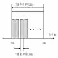
도 1은 현재 이용되는 T-DMB 주파수 대역폭 및 채널 대역폭을 나타내는 도면이다.1 is a diagram illustrating T-DMB frequency bandwidth and channel bandwidth currently used.
도 1에 도시된 바와 같이, T-DMB 주파수 대역폭에는 다수의 채널 대역폭이 포함된다. T-DMB 주파수 대역폭은 42MHz 이지만, 1개 채널 대역폭은 1.536MHz로 매우 좁다. 따라서, 1개 채널이 수신되는 경우, 다른 채널의 채널 대역폭은 이용되지 않으므로, 1개의 소형 안테나를 이용하여 여러 채널을 이용할 수 있는 광대역 수신이 가능하다.As shown in FIG. 1, the T-DMB frequency bandwidth includes a plurality of channel bandwidths. The T-DMB frequency bandwidth is 42MHz, but one channel bandwidth is very narrow at 1.536MHz. Therefore, when one channel is received, since the channel bandwidth of the other channel is not used, wideband reception capable of using multiple channels is possible using one small antenna.
즉, 다수의 공진 주파수를 독립적으로 발생시킴으로써, 1개의 소형 안테나에 서 다수의 채널 수신이 가능하다. 따라서, 소형안테나를 이용한 광대역 수신이 가능하다. 다만, 소형안테나의 대역폭은 도 1의 채널 대역폭 이상이어야 한다.That is, by generating a plurality of resonant frequencies independently, it is possible to receive a plurality of channels in one small antenna. Therefore, broadband reception using a small antenna is possible. However, the bandwidth of the small antenna should be greater than or equal to the channel bandwidth of FIG.
일반적으로, 안테나의 공진 주파수를 조절하는 종래기술은 기생소자 혹은 RF소자를 설치하여 인덕턴스(Inductance) 또는 캐패시턴스(Capacitance)를 변화시킴으로써, 안테나의 리액턴스(Reactance) 값을 0으로 만드는 기술이다.In general, the related art of controlling the resonance frequency of an antenna is a technique of changing a inductance or capacitance by installing a parasitic element or an RF element to zero the reactance value of the antenna.
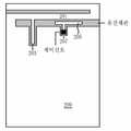
도 2는 종래 기생소자를 이용하는 소형안테나를 나타내는 구성도이다.2 is a block diagram showing a small antenna using a conventional parasitic element.
도 2에 도시된 바와 같이, 기생소자를 이용하는 소형안테나는 바렉터 다이오드, 가변 캐패시턴스를 이용하여 인덕턴스 또는 캐패시턴스를 변화시킴으로써, 공진 주파수를 조절한다.As shown in FIG. 2, the small antenna using the parasitic element adjusts the resonant frequency by changing the inductance or the capacitance by using the varactor diode and the variable capacitance.
상기 기생소자를 이용하는 소형안테나는 도체부(201), 회로 출력부(203), 기생소자(205), 기생소자 스위치부(207) 및 PCB(printed circuit board) 에지 평판(미도시)으로 구성된다. 여기서, PCB 에지 평판(미도시)은 안테나에서 일반적으로 구현되는 회로를 포함하며, 접지선을 포함한다.The small antenna using the parasitic element includes a
상기 도체부(201)는 안테나 엘리먼트로서, 외부로 신호를 송신하거나, 외부로부터 신호를 수신받는 역할을 한다.The
상기 회로 출력부(203)는 상기 PCB 에지 평판(미도시)으로부터 상기 도체부(201)로 전원을 공급한다.The
상기 기생소자(205)는 예를 들어, 바렉터 다이오드, 가변 캐패시턴스 등이 이용될 수 있다.For example, the
상기 기생소자 스위치부(207)는 상기 PCB 에지 평판(미도시)에 의해 제어된 제어신호를 이용하여 상기 기생소자(205)를 상기 PCB 에지 평판(미도시)에 포함된 접지면과 연결한다. 즉, 기생소자 스위치부(207)의 켜짐/꺼짐(on/off)에 따라, 기생소자(205)가 안테나 회로에 연결되거나, 끊어진다.The parasitic
그러나, 바렉터 다이오드 또는 가변 캐패시턴스는 주변 환경(예를 들어, 손, 머리카락에 의한 정전기, 주변 회로 등)에 민감하게 반응하고, 바렉터 다이오드처럼 매 제품마다 바이어스 전압을 일정하게 공급받아야 하는 소자는 일정한 캐패시턴스 값을 유지하기 어려우므로, 일정한 공진 주파수가 발생되기 어렵다. 또한, 기생소자를 접지와 연결하거나 끊을 경우, 리액턴스 값의 변화가 커서, T-DMB, S-DMB, DVB-H, D-TV 등의 모든 채널이 포함되도록 공진주파수를 미세하게 조절하기 어렵다. 게다가, 기생소자의 리액턴스 값은 기생소자의 위치, 모양, 간극, 캐패시턴스, 인던턴스 등을 종합하여 결정되므로, 공진 주파수 변화에 대한 예측이 어렵다.However, the varistor diode or variable capacitance is sensitive to the surrounding environment (for example, static electricity caused by hands, hair, peripheral circuits, etc.), and a device such as a varistor diode that needs to be supplied with a constant bias voltage for each product Since it is difficult to maintain a constant capacitance value, it is difficult to generate a constant resonance frequency. In addition, when the parasitic element is connected to or disconnected from the ground, it is difficult to finely adjust the resonance frequency to include all channels such as T-DMB, S-DMB, DVB-H, and D-TV, because the change in reactance value is large. In addition, the reactance value of the parasitic element is determined by integrating the position, shape, gap, capacitance, inductance, and the like of the parasitic element, and thus it is difficult to predict the change of the resonance frequency.
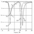
도 3은 도 2의 소형 안테나에서 기생소자 스위치의 on/off에 따른 S11 파라미터를 나타내는 그래프이다.FIG. 3 is a graph illustrating S11 parameters according to on / off of the parasitic element switch in the small antenna of FIG. 2.
안테나는 끊어진 선로로서, 그 끝 단이 특정 주파수에서 공진하도록 함으로 써, 신호가 전반사 되지 않고, 특정 자기장 에너지로 외부에 전송되도록 한다. 즉, 기본적으로 안테나는 입력 포트가 1개인 1 포트장치(1 port device)이다. 따라서, 안테나에서는 입력 반사계수를 의미하는 S11 값만을 가지며, 안테나가 동작되는 주파수에서의 S11 값(dB)이 최소가 되며, S11 값이 최소인 주파수에서는 안테나로 입력된 신호전력이 외부로 최대 복사된다. 즉, S11 값이 최소인 지점에서 임피던스 정합이 가장 잘된다.An antenna is a broken line that causes its end to resonate at a specific frequency so that the signal is not totally reflected but transmitted to the outside with a specific magnetic field energy. That is, the antenna is basically a one port device having one input port. Therefore, the antenna has only the S11 value representing the input reflection coefficient, the S11 value (dB) at the frequency at which the antenna is operated is minimum, and at the minimum S11 value, the signal power input to the antenna is maximum radiated to the outside. do. In other words, the impedance matching is best at the point where S11 is the minimum.
따라서, S11 값이 작을수록, 안테나의 복사 효율이 높고, S11의 첨예도가 작을수록, 안테나에서 이용되는 주파수 대역폭이 넓다는 의미이다.Therefore, the smaller the S11 value, the higher the radiation efficiency of the antenna, and the smaller the sharpness of S11, the wider the frequency bandwidth used in the antenna.
도 3에 도시된 바와 같이, A 그래프는 기생소자 스위치가 꺼진 경우(off)를 나타내며, B 그래프는 기생소자 스위치가 켜진 경우(on)를 나타낸다. A 그래프 및 B 그래프는 모두 제1공진주파수 영역(301a, 301b) 및 제2공진주파수 영역(303a, 303b)를 포함한다. 여기서, 수직축은 S11 값(dB 단위)을 나타내고, 수평축은 주파수(MHz 단위)를 나타낸다.As shown in FIG. 3, the A graph shows when the parasitic switch is turned off (off), and the B graph shows when the parasitic switch is turned on (on). The A graph and the B graph both include first
제1공진주파수 영역 및 제2공진주파수 영역에서 B 그래프(기생소자 스위치가 켜진 경우)가 A 그래프(기생소자 스위치가 꺼진 경우)에 비해 모두 더 작은 S11 값을 갖는다. 즉, 301a의 S11값이 301b의 S11값보다 크며, 303a의 S11값이 303b의 S11값보다 크다. 따라서, 기생소자 스위치가 켜진 경우가 임피던스 정합이 잘 이루어 지고, 안테나 복사 효율이 더 높다.In the first resonant frequency region and the second resonant frequency region, the B graph (when the parasitic element switch is turned on) has a smaller S11 value than the A graph (when the parasitic element switch is turned off). That is, S11 value of 301a is larger than S11 value of 301b, and S11 value of 303a is larger than S11 value of 303b. Therefore, when the parasitic switch is turned on, impedance matching is well achieved and antenna radiation efficiency is higher.
한편 기생소자 스위치의 on/off에 따라, 제1공진주파수 영역(301a와 301b 사이)의 주파수는 미세한 차이가 발생하나, 제2공진주파수 영역(303a와 303b 사이)의 주파수는 변화의 폭이 크다. 따라서, 제1공진주파수 영역 내에서 채널변화를 위한 미세조절은 가능하지만, 제2공진주파수 영역 내에서 채널변화를 위한 미세조절은 불가능하다.On the other hand, according to the on / off of the parasitic element switch, a minute difference occurs in the frequency of the first resonance frequency region (301a and 301b), but the frequency of the second resonance frequency region (303a and 303b) has a large range of change. . Therefore, fine adjustment for channel change in the first resonance frequency region is possible, but fine adjustment for channel change in the second resonance frequency region is impossible.
따라서, 도 2의 기생소자를 이용하는 소형안테나의 경우에는, 기생소자 스위치의 on/off에 따라, 제1공진주파수 영역의 변화는 미세하고, 제2공진주파수 영역의 변화가 커서, 제2공진주파수 영역 내의 송수신 신호에 대한 미세조절이 어려운 문제점이 발생한다.Therefore, in the case of the small antenna using the parasitic element of FIG. 2, the change in the first resonant frequency region is minute and the change in the second resonant frequency region is large due to the on / off of the parasitic element switch. It is difficult to finely adjust the transmission and reception signals in the region.
상기에서 설명한 바와 같이, 종래 기생소자를 이용하는 소형 안테나에서 발생하는 문제점을 해결하기 위해 다수의 공진주파수가 발생되고, 임의로 선택된 공진주파수에서 미세한 주파수 조절도 가능한 다중 공진 소형 안테나가 요구된다.As described above, in order to solve the problems occurring in the conventional small antenna using parasitic elements, a plurality of resonant frequencies are generated, and a multi-resonant small antenna capable of fine frequency adjustment at an arbitrarily selected resonant frequency is required.
본 발명은 상기 요구에 부응하기 위하여 제안된 것으로, 기생소자 및 다중 급전단자를 이용하여, 공진주파수를 크게 가변하고, 임의로 선택된 공진주파수 내에서 미세한 주파수 조절이 가능한 다중 공진 소형 안테나를 제공하는데 목적이 있 다.SUMMARY OF THE INVENTION The present invention has been proposed to meet the above requirements, and an object of the present invention is to provide a multi-resonant compact antenna capable of varying a resonant frequency with a parasitic element and a multi-feed terminal, and having a fine frequency control within a randomly selected resonant frequency. have.
상기 목적을 달성하기 위한 본 발명은, 안테나에 있어서, 안테나 소자부; 상기 안테나 소자부로 급전할 수 있는 복수의 급전부; 안테나 회로가 배치되는 기판과 상기 안테나 소자부 사이의 유전 영역 내에 배치되는 기생소자부; 상기 안테나 소자부로 급전하기 위해, 상기 복수의 급전부 중 어느 하나를 선택적으로 상기 안테나 소자부와 연결시키는 급전 스위치부; 및 상기 기생소자부를 제어하는 기생소자 스위치부를 포함하되, 상기 복수의 급전부는 각각 상기 안테나 소자부의 총 길이가 달라지도록 배치되는 안테나를 제공한다.The present invention for achieving the above object, the antenna, the antenna element unit; A plurality of feeders capable of feeding power to the antenna element portion; A parasitic element portion disposed in a dielectric region between the substrate on which the antenna circuit is disposed and the antenna element portion; A feed switch unit configured to selectively connect any one of the plurality of feed units with the antenna element unit to feed the antenna element unit; And a parasitic element switch unit for controlling the parasitic element unit, wherein the plurality of power supply units provide an antenna arranged such that the total length of the antenna element unit is different.
본 발명은 기생소자 및 다중 급전단자를 안테나 내부에 설치한 소형 안테나를 제공함으로써, 공진주파수를 크게 가변하고, 다중 대역, 즉 광대역 수신이 가능하고, 임의로 선택된 공진주파수 내에서 미세한 주파수 조절이 가능한 소형 안테나를 제공할 수 있다.The present invention provides a small antenna in which parasitic elements and multiple feed terminals are provided inside the antenna, whereby the resonance frequency is largely variable, multiband, that is, wideband reception is possible, and the fine frequency control is possible within the arbitrarily selected resonance frequency. An antenna can be provided.
상술한 목적, 특징들 및 장점은 첨부된 도면과 관련한 다음의 상세한 설명을 통하여 보다 분명해 질 것이다. 이하, 첨부된 도면을 참조하여 본 발명에 따른 바 람직한 일실시예를 상세히 설명한다.The above-mentioned objects, features and advantages will become more apparent from the following detailed description in conjunction with the accompanying drawings. Hereinafter, exemplary embodiments of the present invention will be described in detail with reference to the accompanying drawings.
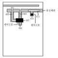
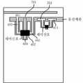
도 4는 본 발명에 따른 기생소자 및 다중 급전단자를 이용하는 소형안테나의 일실시예 구성도이다.4 is a configuration diagram of an embodiment of a small antenna using the parasitic element and the multi-feed terminal according to the present invention.
도 4에 도시된 바와 같이, 본 발명에 따른 소형 안테나는 도체부(401), 제1급전단자(403), 제2급전단자(405), RF 스위치부(407), 회로출력부(409), 기생소자(411), 기생소자 스위치부(413) 및 PCB 에지 평판(미도시)를 포함한다. 여기서, PCB 에지 평판(미도시)은 안테나에서 일반적으로 구현되는 회로(예를 들어, 증폭기, 믹서, AD변환기 등 RF소자와 연결되는 구조)를 포함하며, 접지선을 포함한다.As shown in FIG. 4, the small antenna according to the present invention includes a
상기 도체부(401)는 안테나 엘리먼트로서, 외부로 신호를 송신하거나, 외부로부터 신호를 수신받는다.The
상기 제1급전단자(403) 및 제2급전단자(405)는 상기 회로출력부(409)와 도체부(401)를 연결하며, 각 급전단자에 따라 도체부(401)의 총 길이(급전지점부터 안테나 끝단까지의 길이)가 변화될 수 있도록 설치된다.The
상기 RF 스위치부(407)는 상기 PCB 에지 평판(미도시)으로부터 전송된 제어신호를 이용하여 회로출력부(409)를 제1급전단자(403) 또는 제2급전단자(405) 중 하나와 선택적으로 연결한다. 회로출력부(409)가 제1급전단자(403) 또는 제2급전단자(405)와 연결됨으로써, 도체부(401)의 총 길이(급전지점부터 안테나끝단까지의 길이)가 바뀌어 안테나의 공진 길이도 바뀌게 된다.The
여기서, 상기 도 4는 제1급전단자(403) 및 제2급전단자(405) 2개의 급전단자를 나타내고 있으나, 급전단자는 실시예에 따라 3개, 4개, 5개 등 임의로 설치될 수 있다. 다만, 급전단자의 선택에 따라 도체부 총 길이가 변화되어야 한다. 하기 도 8에서 상세하게 설명한다.4 illustrates two feed terminals of the
상기 회로 출력부(409)는 급전지점으로서, 연결된 제1급전단자(403) 또는 제2급전단자(405)를 통해 상기 PCB 에지 평판(미도시)으로부터 상기 도체부(401)로 전원이 공급된다.The
상기 기생소자(411)는 예를 들어, 바렉터 다이오드, 가변 캐패시턴스 등이 이용될 수 있다. 또한, 상기 기생소자(411)는 도체부(401)와 PCB 에지 평판(미도시) 사이에 존재하는 유전체판 내부에 위치한다.For example, the
여기서, 상기 도 4는 하나의 기생소자(411)를 나타내고 있으나, 실시예에 따라 다수의 기생소자가 설치되고, 기생소자 스위치부(413)를 이용하여 제어될 수 있다. 하기 도 7에서 상세하게 설명한다.4 illustrates one
상기 기생소자 스위치부(413)는 상기 PCB 에지 평판(미도시)에 의해 제어된 제어신호를 이용하여 상기 기생소자(411)를 상기 PCB 에지 평판(미도시)에 포함된 접지면과 연결한다. 즉, 기생소자 스위치부(413)의 켜짐/꺼짐(on/off)에 따라, 기생소자(411)가 접지면에 연결되거나, 끊어진다.The parasitic
여기서, 기생소자 스위치부(413)가 켜지면(on), 도체부(401)와 PCB 에지 평판(미도시) 사이의 간격이 좁아지고, 따라서 캐패시턴스 성분이 증가하므로, 리액턴스 값이 감소한다. 반대로, 기생소자 스위치부(413)가 꺼지면(off), 도체부(401)와 PCB 에지 평판(미도시) 사이의 간격이 넓어지고, 따라서 캐패시턴스 성분이 감소하고, 리액턴스 값이 증가한다.Here, when the parasitic
즉, 기생소자 스위치 on/off에 따라 안테나의 리액턴스 값이 변화되어, 주파수의 미세조절이 가능하게 된다.That is, the reactance value of the antenna is changed according to the parasitic element switch on / off, thereby enabling fine adjustment of the frequency.
RF 스위치부(407) 또는 기생소자 스위치부(413)는 LC스위치의 공진주파수 정보 또는 중간주파수 변환장치에 의해 선택되어 믹서로 인가되는 국부 발진 주파수 정보에 기초하여, 제어된다. 또한 RF신호 또는 중간주파수 신호의 신호대잡음비(signal to noise ratio)를 궤환시켜 최대치가 되도록 스위칭될 수 있다.The
상기 RF 스위치부(407)가 동시에 다수의 급전단자와 연결되는 경우, 하나의 안테나로 볼 수 있으므로, 소형 안테나의 최대 대역폭에 의해서 대역폭이 제한을 받는다. 따라서, 본 발명에 따른 소형안테나에서 회로출력부(409)는 하나의 급전단자와 연결되고, 나머지 급전단자와는 모두 끊어진다.When the
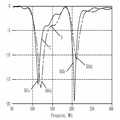
도 5는 도 4의 소형안테나의 기생소자 스위치부(413)가 켜진(on) 상태일 때, 급전단자에 따른 S11 파라미터를 나타내는 그래프이다.FIG. 5 is a graph illustrating S11 parameters according to a power supply terminal when the parasitic
도 5에 도시된 바와 같이, C 그래프는 기생소자 스위치가 켜진(on) 상태에서 회로출력부(409)가 제1급전단자(403)와 연결된 경우, 제1공진주파수 영역(501c) 및 제2공진주파수 영역(503c)를 나타내고, D 그래프는 기생소자 스위치가 켜진(on) 상태에서 회로출력부(409)가 제2급전단자(405)와 연결된 경우, 제1공진주파수 영역(501d) 및 제2공진주파수 영역(503d)를 나타낸다. 여기서 수직축은 S11 값(dB 단위)을 나타내고, 수평축은 주파수(MHz 단위)를 나타낸다.As shown in FIG. 5, the C graph shows the first
기생소자 스위치가 켜진(on) 경우, C 그래프 및 D 그래프 제1공진주파수 영역(501c, 501d) 사이의 변화의 폭이 작고, C 그래프 및 D 그래프 제2공진주파수 영역(503c, 503d) 사이의 변화의 폭이 작다. 또한, C 그래프 및 D 그래프 제1공진주파수 영역(501c, 501d)의 S11 값이 -10dB보다 훨씬 작은 값을 갖는다.When the parasitic element switch is turned on, the width of the change between the C graph and the D graph first
즉, 기생소자 스위치가 켜진(on) 경우, 도 4의 소형안테나에서 제1급전단자(403)에 연결된 경우와 제2급전단자(405)에 연결된 경우 공진주파수 변화의 폭이 작으므로, 주파수 미세 조절이 용이하다. 또한, 제1공진주파수(501c, 501d)에 대해서는 S11 값이 작으므로, 임피던스 정합이 잘 이루어져 임피던스 부정합으로 인한 반사손실을 최소화할 수 있고, 안테나의 효율이 높아진다.That is, when the parasitic element switch is turned on, when the parasitic element switch is connected to the
따라서, 기생소자 스위치가 켜진(on) 경우에는, 제1공진주파수에 해당되는 신호에 대해 주파수 미세조절이 가능하고, 안테나효율이 높다.Accordingly, when the parasitic element switch is turned on, frequency fine adjustment is possible for the signal corresponding to the first resonance frequency, and antenna efficiency is high.
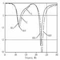
도 6은 도 4의 소형안테나의 기생소자 스위치가 꺼진(off) 상태일 때, 급전단자에 따른 S11 파라미터를 나타내는 그래프이다.FIG. 6 is a graph illustrating S11 parameters according to a power supply terminal when the parasitic element switch of the small antenna of FIG. 4 is turned off.
도 6에 도시된 바와 같이, E 그래프는 기생소자 스위치가 꺼진(off) 상태에서 회로출력부(409)가 제1급전단자(403)와 연결된 경우, 제1공진주파수 영역(601e) 및 제2공진주파수 영역(603e)를 나타내고, F 그래프는 기생소자 스위치가 꺼진(off) 상태에서 회로출력부(409)가 제2급전단자(405)와 연결된 경우, 제1공진주파수 영역(601f) 및 제2공진주파수 영역(603f)를 나타낸다. 여기서 수직축은 S11 값(dB 단위)을 나타내고, 수평축은 주파수(MHz 단위)를 나타낸다.As shown in FIG. 6, the E graph shows the first
기생소자 스위치가 꺼진(off) 경우, E 그래프 및 F 그래프 제1공진주파수 영역(601e, 601f) 사이의 변화의 폭이 작고, E 그래프 및 F 그래프 제2공진주파수 영역(603e, 603f) 사이의 변화의 폭이 작다. 또한, E 그래프 및 F 그래프 제2공진주파수 영역(603e, 603f)의 S11 값이 -10dB보다 훨씬 작은 값을 갖는다.When the parasitic element switch is off, the width of the change between the E graph and the F graph first
즉, 기생소자 스위치가 꺼진(off) 경우, 도 4의 소형안테나에서 제1급전단자(403)에 연결된 경우와 제2급전단자(405)에 연결된 경우 공진주파수 변화의 폭이 작으므로, 주파수 미세 조절이 용이하다. 또한, 제2공진주파수(603e, 603f)에 대해서는 S11 값이 작으므로, 임피던스 정합이 잘 이루어져 임피던스 부정합으로 인한 반사손실을 최소화할 수 있고, 안테나의 효율이 높아진다.That is, when the parasitic element switch is turned off, when the parasitic element switch is connected to the
따라서, 기생소자 스위치가 꺼진(off) 경우에는, 제2공진주파수에 해당되는 신호에 대해 주파수 미세조절이 가능하고, 안테나효율이 높다.Therefore, when the parasitic element switch is turned off, fine tuning of the signal corresponding to the second resonance frequency is possible and the antenna efficiency is high.
한편, 도 5 및 도 6에 도시된 바와 같이, 제1급전단자(403)에 연결된 경우, 기생소자 스위치 on/off에 따른 변화를 살펴보면, 제1공진주파수 사이(501c와 601e사이)의 변화 폭 및 제2공진주파수 사이(503c와 603e사이)의 변화 폭이 약 10~20MHz로 도 1에 도시된 채널변화 폭에 비해 매우 크다. 또한, 제2급전단자(405)에 연결된 경우도, 제1공진주파수 사이(501d와 601f사이)의 변화 폭 및 제2공진주파수 사이(503d와 603f사이)의 변화 폭이 매우 크다.On the other hand, as shown in Figure 5 and 6, when connected to the
즉, 기생소자 스위치 on/off에 따라 기생소자의 캐패시턴스 값이 변화되고, 안테나의 리액턴스가 변화되어, 공진 주파수를 큰 폭으로 가변할 수 있다.That is, the capacitance value of the parasitic element changes according to the parasitic element switch on / off, the reactance of the antenna changes, and the resonance frequency can be largely changed.
따라서, 기생소자를 이용하여, 큰 폭으로 주파수를 가변시킬 수 있고, 큰 폭으로 가변된 공진주파수내에서, 다수의 급전단자를 이용하여, 미세하게 채널을 변화시킬 수 있다. 따라서, 미세한 채널 변경은 물론, 큰 폭의 채널 변경도 가능하며, 기생소자의 선택에 따라 다른 서비스를 위한 주파수 대역으로의 변경도 가능하다.Therefore, the parasitic element can be used to vary the frequency by a large width, and the channel can be changed finely by using a plurality of feed terminals within the resonant frequency which is changed by the large width. Therefore, not only a minute channel change but also a large channel change is possible, and a change to a frequency band for another service can be made according to the selection of parasitic elements.
도 5 및 도 6에 도시된 바와 같이, 기생소자 스위치의 on/off에 따라 제1공진주파수 또는 제2공진주파수를 효과적으로 이용할 수 있다. 또한, 도 4에 도시된 안테나의 길이를 절반으로 줄이면, 사용주파수 대역이 2배가 되므로, T- DMB(174MHz~216MHz), DVB-H(400MHz~600MHz)을 수신할 수 있다.5 and 6, the first resonant frequency or the second resonant frequency may be effectively used according to on / off of the parasitic element switch. In addition, if the length of the antenna shown in FIG. 4 is cut in half, the frequency band used is doubled, so that T-DMB (174 MHz to 216 MHz) and DVB-H (400 MHz to 600 MHz) can be received.
도 4 내지 도 6에 도시된 바와 같이, 본 발명에 따른 소형안테나는 기생소자를 이용함으로써 공진주파수를 큰 폭으로 가변할 수 있고, 다수의 급전단자를 이용하여 안테나의 총 길이를 변화시킴으로써 공진주파수의 미세조절이 가능하다.4 to 6, the small antenna according to the present invention can vary the resonant frequency by using a parasitic element, and the resonant frequency by changing the total length of the antenna using a plurality of feed terminals Fine adjustment of is possible.
도 7은 본 발명에 따른 기생소자 및 다중 급전단자를 이용하는 소형안테나를 나타내는 또 다른 일실시예 구성도로서, 도 4의 소형안테나에 제3급전단자(701) 및 제2기생소자(703)가 추가된 경우이다.FIG. 7 is a diagram illustrating another embodiment of a small antenna using a parasitic element and a multi-feed terminal according to the present invention. In the small antenna of FIG. If it is added.
도 7에 도시된 바와 같이, 본 발명에 따른 소형 안테나는 하나의 안테나에 다수의 급전단자 및 다수의 기생소자를 포함한다. 여기서, 기생소자(411)는 제2기생소자와 구분하기 위하여 이하 제1기생소자(411)라고 칭한다.As shown in FIG. 7, the small antenna according to the present invention includes a plurality of feed terminals and a plurality of parasitic elements in one antenna. Herein, the
즉, RF 스위치부(407)는 회로출력부(409)를 제1급전단자(403), 제2급전단자(405) 및 제3근접단자(701) 중 하나와 선택적으로 연결하고, 기생소자 스위치부(413)는 제1기생소자(411) 및 제2기생소자(903)를 제어한다. 여기서, 총 안테나 길이 변화에 의해 공진주파수가 선택되는 특징에 따라, 급전단자 3개에 따른 안테나 총 길이의 변화에 따라 미세한 주파수 차이를 갖는 공진주파수가 3개 발생된다.That is, the
여기서, 상기 기생소자 스위치부(413)는 1개의 급전단자만 연결해야 하는 상 기 RF 스위치부(407)와 달리, 제1기생소자(411) 및 제2기생소자(703) 중 하나를 선택적으로 접지면과 연결할 수도 있고, 동시에 제1기생소자(411) 및 제2기생소자(703) 모두를 접지면에 연결할 수 있다. 이와 같이 기생소자를 선택적 또는 동시에 접지면에 연결하는 것은, 제1공진주파수(501c, 501d, 601e, 601f) 또는 제2공진주파수(503c, 503d, 603e, 603f)에 해당되는 신호를 선택적으로 송수신하고, 임피던스 정합을 유지하기 위함이다.Here, the parasitic
상기 도 4 내지 도 7에서 설명된, 본 발명에 따른 기생소자 및 다중 급전단자를 이용하는 소형안테나는 평판형 역 에프 안테나(Planar Inverted-F Antenna, PIFA) 등과 같은 역 F 안테나, 민더형 안테나, 헬리컬 안테나, 스프링 타입의 루프안테나 등에서 적용될 수 있다. 또한, 스파이럴 끝단 장하형 모노폴(Spiral Top Loaded Monopole Antenna: STLA) 안테나, 캐패시터 판 안테나(Capacitor-Plate Antenna), 다중소자 끝단 장하형 모노폴 안테나(Multi-Element Top-Loaded Monopole Antenna) 등 1/4파장 이하의 소형 안테나에서도 적용될 수 있다.4 to 7, the small antenna using the parasitic element and the multi-feed terminal according to the present invention is an inverted-F antenna such as a planar inverted-F antenna (PIFA), a meander antenna, a helical It can be applied to an antenna, a loop antenna of a spring type, or the like. In addition, quarter wavelengths include spiral top loaded monopole antennas (STLA) antennas, capacitor-plate antennas, and multi-element top-loaded monopole antennas. It can be applied to the following small antennas.
상술한 바와 같은 본 발명의 방법은 프로그램으로 구현되어 컴퓨터로 읽을 수 있는 형태로 기록매체(씨디롬, 램, 롬, 플로피 디스크, 하드 디스크, 광자기 디스크 등)에 저장될 수 있다. 이러한 과정은 본 발명이 속하는 기술 분야에서 통상의 지식을 가진 자가 용이하게 실시할 수 있으므로 더 이상 상세히 설명하지 않기로 한다.The method of the present invention as described above may be embodied as a program and stored in a computer-readable recording medium (such as a CD-ROM, a RAM, a ROM, a floppy disk, a hard disk, or a magneto-optical disk). Since this process can be easily implemented by those skilled in the art will not be described in more detail.
이상에서 설명한 본 발명은 전술한 실시예 및 첨부된 도면에 의해 한정되는 것이 아니고, 본 발명의 기술적 사상을 벗어나지 않는 범위 내에서 여러 가지 치환, 변형 및 변경이 가능하다는 것이 본 발명이 속하는 기술분야에서 통상의 지식을 가진 자에게 있어 명백할 것이다.The present invention described above is not limited to the above-described embodiments and the accompanying drawings, and various substitutions, modifications, and changes are possible in the art without departing from the technical spirit of the present invention. It will be clear to those of ordinary knowledge.
도 1은 현재 이용되는 T-DMB 주파수 대역폭 및 채널 대역폭을 나타내는 도면.1 is a diagram showing T-DMB frequency bandwidth and channel bandwidth currently used.
도 2는 종래 기생소자를 이용하는 소형안테나를 나타내는 일실시예 구성도.Figure 2 is a configuration diagram of an embodiment showing a small antenna using a conventional parasitic element.
도 3은 도 2의 소형 안테나에서 기생소자 스위치의 on/off에 따른 S11 파라미터를 나타내는 그래프.3 is a graph illustrating S11 parameters according to on / off of a parasitic element switch in the small antenna of FIG.
도 4는 본 발명에 따른 기생소자 및 다중 급전단자를 이용하는 소형안테나를 나타내는 일실시예 구성도.Figure 4 is a configuration diagram showing a small antenna using a parasitic element and a multi-feed terminal according to the present invention.
도 5는 도 4의 소형안테나의 기생소자 스위치부(413)가 켜진(on) 상태일 때, 급전단자에 따른 S11 파라미터를 나타내는 그래프.FIG. 5 is a graph illustrating S11 parameters according to a power supply terminal when the parasitic
도 6은 도 4의 소형안테나의 기생소자 스위치가 꺼진(off) 상태일 때, 급전단자에 따른 S11 파라미터를 나타내는 그래프.FIG. 6 is a graph illustrating S11 parameters according to a feed terminal when the parasitic element switch of the small antenna of FIG. 4 is turned off. FIG.
도 7은 본 발명에 따른 기생소자 및 다중 급전단자를 이용하는 소형안테나를 나타내는 또 다른 일실시예 구성도.Figure 7 is another embodiment configuration showing a small antenna using a parasitic element and a multi-feed terminal in accordance with the present invention.
Claims (16)
Translated fromKoreanPriority Applications (2)
| Application Number | Priority Date | Filing Date | Title |
|---|---|---|---|
| EP07833611AEP2087551A4 (en) | 2006-10-26 | 2007-10-26 | MULTI-RESONANT ANTENNA |
| PCT/KR2007/005302WO2008051044A1 (en) | 2006-10-26 | 2007-10-26 | Multi resonant antenna |
Applications Claiming Priority (2)
| Application Number | Priority Date | Filing Date | Title |
|---|---|---|---|
| KR20060104642 | 2006-10-26 | ||
| KR1020060104642 | 2006-10-26 |
Publications (2)
| Publication Number | Publication Date |
|---|---|
| KR20080038031A KR20080038031A (en) | 2008-05-02 |
| KR100989064B1true KR100989064B1 (en) | 2010-10-25 |
Family
ID=39646859
Family Applications (1)
| Application Number | Title | Priority Date | Filing Date |
|---|---|---|---|
| KR1020070107738AExpired - Fee RelatedKR100989064B1 (en) | 2006-10-26 | 2007-10-25 | Multiple resonant antenna |
Country Status (3)
| Country | Link |
|---|---|
| EP (1) | EP2087551A4 (en) |
| KR (1) | KR100989064B1 (en) |
| WO (1) | WO2008051044A1 (en) |
Cited By (144)
| Publication number | Priority date | Publication date | Assignee | Title |
|---|---|---|---|---|
| KR101393829B1 (en)* | 2012-10-04 | 2014-05-12 | 엘지이노텍 주식회사 | Communication terminal, antenna apparatus thereof, and driving method thereof |
| US9608740B2 (en) | 2015-07-15 | 2017-03-28 | At&T Intellectual Property I, L.P. | Method and apparatus for launching a wave mode that mitigates interference |
| US9615269B2 (en) | 2014-10-02 | 2017-04-04 | At&T Intellectual Property I, L.P. | Method and apparatus that provides fault tolerance in a communication network |
| US9628116B2 (en) | 2015-07-14 | 2017-04-18 | At&T Intellectual Property I, L.P. | Apparatus and methods for transmitting wireless signals |
| US9640850B2 (en) | 2015-06-25 | 2017-05-02 | At&T Intellectual Property I, L.P. | Methods and apparatus for inducing a non-fundamental wave mode on a transmission medium |
| US9667317B2 (en) | 2015-06-15 | 2017-05-30 | At&T Intellectual Property I, L.P. | Method and apparatus for providing security using network traffic adjustments |
| US9674711B2 (en) | 2013-11-06 | 2017-06-06 | At&T Intellectual Property I, L.P. | Surface-wave communications and methods thereof |
| US9685992B2 (en) | 2014-10-03 | 2017-06-20 | At&T Intellectual Property I, L.P. | Circuit panel network and methods thereof |
| US9692101B2 (en) | 2014-08-26 | 2017-06-27 | At&T Intellectual Property I, L.P. | Guided wave couplers for coupling electromagnetic waves between a waveguide surface and a surface of a wire |
| US9699785B2 (en) | 2012-12-05 | 2017-07-04 | At&T Intellectual Property I, L.P. | Backhaul link for distributed antenna system |
| US9705610B2 (en) | 2014-10-21 | 2017-07-11 | At&T Intellectual Property I, L.P. | Transmission device with impairment compensation and methods for use therewith |
| US9705561B2 (en) | 2015-04-24 | 2017-07-11 | At&T Intellectual Property I, L.P. | Directional coupling device and methods for use therewith |
| US9722318B2 (en) | 2015-07-14 | 2017-08-01 | At&T Intellectual Property I, L.P. | Method and apparatus for coupling an antenna to a device |
| US9729197B2 (en) | 2015-10-01 | 2017-08-08 | At&T Intellectual Property I, L.P. | Method and apparatus for communicating network management traffic over a network |
| US9735833B2 (en) | 2015-07-31 | 2017-08-15 | At&T Intellectual Property I, L.P. | Method and apparatus for communications management in a neighborhood network |
| US9742462B2 (en) | 2014-12-04 | 2017-08-22 | At&T Intellectual Property I, L.P. | Transmission medium and communication interfaces and methods for use therewith |
| US9742521B2 (en) | 2014-11-20 | 2017-08-22 | At&T Intellectual Property I, L.P. | Transmission device with mode division multiplexing and methods for use therewith |
| US9748626B2 (en) | 2015-05-14 | 2017-08-29 | At&T Intellectual Property I, L.P. | Plurality of cables having different cross-sectional shapes which are bundled together to form a transmission medium |
| US9749053B2 (en) | 2015-07-23 | 2017-08-29 | At&T Intellectual Property I, L.P. | Node device, repeater and methods for use therewith |
| US9749013B2 (en) | 2015-03-17 | 2017-08-29 | At&T Intellectual Property I, L.P. | Method and apparatus for reducing attenuation of electromagnetic waves guided by a transmission medium |
| US9762289B2 (en) | 2014-10-14 | 2017-09-12 | At&T Intellectual Property I, L.P. | Method and apparatus for transmitting or receiving signals in a transportation system |
| US9769020B2 (en) | 2014-10-21 | 2017-09-19 | At&T Intellectual Property I, L.P. | Method and apparatus for responding to events affecting communications in a communication network |
| US9768833B2 (en) | 2014-09-15 | 2017-09-19 | At&T Intellectual Property I, L.P. | Method and apparatus for sensing a condition in a transmission medium of electromagnetic waves |
| US9769128B2 (en) | 2015-09-28 | 2017-09-19 | At&T Intellectual Property I, L.P. | Method and apparatus for encryption of communications over a network |
| US9780834B2 (en) | 2014-10-21 | 2017-10-03 | At&T Intellectual Property I, L.P. | Method and apparatus for transmitting electromagnetic waves |
| US9787412B2 (en) | 2015-06-25 | 2017-10-10 | At&T Intellectual Property I, L.P. | Methods and apparatus for inducing a fundamental wave mode on a transmission medium |
| US9793955B2 (en) | 2015-04-24 | 2017-10-17 | At&T Intellectual Property I, Lp | Passive electrical coupling device and methods for use therewith |
| US9793951B2 (en) | 2015-07-15 | 2017-10-17 | At&T Intellectual Property I, L.P. | Method and apparatus for launching a wave mode that mitigates interference |
| US9793954B2 (en) | 2015-04-28 | 2017-10-17 | At&T Intellectual Property I, L.P. | Magnetic coupling device and methods for use therewith |
| US9800327B2 (en) | 2014-11-20 | 2017-10-24 | At&T Intellectual Property I, L.P. | Apparatus for controlling operations of a communication device and methods thereof |
| US9820146B2 (en) | 2015-06-12 | 2017-11-14 | At&T Intellectual Property I, L.P. | Method and apparatus for authentication and identity management of communicating devices |
| US9838078B2 (en) | 2015-07-31 | 2017-12-05 | At&T Intellectual Property I, L.P. | Method and apparatus for exchanging communication signals |
| US9838896B1 (en) | 2016-12-09 | 2017-12-05 | At&T Intellectual Property I, L.P. | Method and apparatus for assessing network coverage |
| US9847850B2 (en) | 2014-10-14 | 2017-12-19 | At&T Intellectual Property I, L.P. | Method and apparatus for adjusting a mode of communication in a communication network |
| US9847566B2 (en) | 2015-07-14 | 2017-12-19 | At&T Intellectual Property I, L.P. | Method and apparatus for adjusting a field of a signal to mitigate interference |
| US9853342B2 (en) | 2015-07-14 | 2017-12-26 | At&T Intellectual Property I, L.P. | Dielectric transmission medium connector and methods for use therewith |
| US9860075B1 (en) | 2016-08-26 | 2018-01-02 | At&T Intellectual Property I, L.P. | Method and communication node for broadband distribution |
| US9865911B2 (en) | 2015-06-25 | 2018-01-09 | At&T Intellectual Property I, L.P. | Waveguide system for slot radiating first electromagnetic waves that are combined into a non-fundamental wave mode second electromagnetic wave on a transmission medium |
| US9866309B2 (en) | 2015-06-03 | 2018-01-09 | At&T Intellectual Property I, Lp | Host node device and methods for use therewith |
| US9866276B2 (en) | 2014-10-10 | 2018-01-09 | At&T Intellectual Property I, L.P. | Method and apparatus for arranging communication sessions in a communication system |
| US9871283B2 (en) | 2015-07-23 | 2018-01-16 | At&T Intellectual Property I, Lp | Transmission medium having a dielectric core comprised of plural members connected by a ball and socket configuration |
| US9871282B2 (en) | 2015-05-14 | 2018-01-16 | At&T Intellectual Property I, L.P. | At least one transmission medium having a dielectric surface that is covered at least in part by a second dielectric |
| US9871558B2 (en) | 2014-10-21 | 2018-01-16 | At&T Intellectual Property I, L.P. | Guided-wave transmission device and methods for use therewith |
| US9876570B2 (en) | 2015-02-20 | 2018-01-23 | At&T Intellectual Property I, Lp | Guided-wave transmission device with non-fundamental mode propagation and methods for use therewith |
| US9876264B2 (en) | 2015-10-02 | 2018-01-23 | At&T Intellectual Property I, Lp | Communication system, guided wave switch and methods for use therewith |
| US9882257B2 (en) | 2015-07-14 | 2018-01-30 | At&T Intellectual Property I, L.P. | Method and apparatus for launching a wave mode that mitigates interference |
| US9887447B2 (en) | 2015-05-14 | 2018-02-06 | At&T Intellectual Property I, L.P. | Transmission medium having multiple cores and methods for use therewith |
| US9893795B1 (en) | 2016-12-07 | 2018-02-13 | At&T Intellectual Property I, Lp | Method and repeater for broadband distribution |
| US9906269B2 (en) | 2014-09-17 | 2018-02-27 | At&T Intellectual Property I, L.P. | Monitoring and mitigating conditions in a communication network |
| US9904535B2 (en) | 2015-09-14 | 2018-02-27 | At&T Intellectual Property I, L.P. | Method and apparatus for distributing software |
| US9913139B2 (en) | 2015-06-09 | 2018-03-06 | At&T Intellectual Property I, L.P. | Signal fingerprinting for authentication of communicating devices |
| US9911020B1 (en) | 2016-12-08 | 2018-03-06 | At&T Intellectual Property I, L.P. | Method and apparatus for tracking via a radio frequency identification device |
| US9912382B2 (en) | 2015-06-03 | 2018-03-06 | At&T Intellectual Property I, Lp | Network termination and methods for use therewith |
| US9912033B2 (en) | 2014-10-21 | 2018-03-06 | At&T Intellectual Property I, Lp | Guided wave coupler, coupling module and methods for use therewith |
| US9912419B1 (en) | 2016-08-24 | 2018-03-06 | At&T Intellectual Property I, L.P. | Method and apparatus for managing a fault in a distributed antenna system |
| US9912027B2 (en) | 2015-07-23 | 2018-03-06 | At&T Intellectual Property I, L.P. | Method and apparatus for exchanging communication signals |
| US9917341B2 (en) | 2015-05-27 | 2018-03-13 | At&T Intellectual Property I, L.P. | Apparatus and method for launching electromagnetic waves and for modifying radial dimensions of the propagating electromagnetic waves |
| US9930668B2 (en) | 2013-05-31 | 2018-03-27 | At&T Intellectual Property I, L.P. | Remote distributed antenna system |
| US9927517B1 (en) | 2016-12-06 | 2018-03-27 | At&T Intellectual Property I, L.P. | Apparatus and methods for sensing rainfall |
| US9948354B2 (en) | 2015-04-28 | 2018-04-17 | At&T Intellectual Property I, L.P. | Magnetic coupling device with reflective plate and methods for use therewith |
| US9948355B2 (en) | 2014-10-21 | 2018-04-17 | At&T Intellectual Property I, L.P. | Apparatus for providing communication services and methods thereof |
| US9948333B2 (en) | 2015-07-23 | 2018-04-17 | At&T Intellectual Property I, L.P. | Method and apparatus for wireless communications to mitigate interference |
| US9954287B2 (en) | 2014-11-20 | 2018-04-24 | At&T Intellectual Property I, L.P. | Apparatus for converting wireless signals and electromagnetic waves and methods thereof |
| US9954286B2 (en) | 2014-10-21 | 2018-04-24 | At&T Intellectual Property I, L.P. | Guided-wave transmission device with non-fundamental mode propagation and methods for use therewith |
| US9967173B2 (en) | 2015-07-31 | 2018-05-08 | At&T Intellectual Property I, L.P. | Method and apparatus for authentication and identity management of communicating devices |
| US9973940B1 (en) | 2017-02-27 | 2018-05-15 | At&T Intellectual Property I, L.P. | Apparatus and methods for dynamic impedance matching of a guided wave launcher |
| US9991580B2 (en) | 2016-10-21 | 2018-06-05 | At&T Intellectual Property I, L.P. | Launcher and coupling system for guided wave mode cancellation |
| US9999038B2 (en) | 2013-05-31 | 2018-06-12 | At&T Intellectual Property I, L.P. | Remote distributed antenna system |
| US9998870B1 (en) | 2016-12-08 | 2018-06-12 | At&T Intellectual Property I, L.P. | Method and apparatus for proximity sensing |
| US9997819B2 (en) | 2015-06-09 | 2018-06-12 | At&T Intellectual Property I, L.P. | Transmission medium and method for facilitating propagation of electromagnetic waves via a core |
| US10009063B2 (en) | 2015-09-16 | 2018-06-26 | At&T Intellectual Property I, L.P. | Method and apparatus for use with a radio distributed antenna system having an out-of-band reference signal |
| US10009067B2 (en) | 2014-12-04 | 2018-06-26 | At&T Intellectual Property I, L.P. | Method and apparatus for configuring a communication interface |
| US10009065B2 (en) | 2012-12-05 | 2018-06-26 | At&T Intellectual Property I, L.P. | Backhaul link for distributed antenna system |
| US10020844B2 (en) | 2016-12-06 | 2018-07-10 | T&T Intellectual Property I, L.P. | Method and apparatus for broadcast communication via guided waves |
| US10027398B2 (en) | 2015-06-11 | 2018-07-17 | At&T Intellectual Property I, Lp | Repeater and methods for use therewith |
| US10027397B2 (en) | 2016-12-07 | 2018-07-17 | At&T Intellectual Property I, L.P. | Distributed antenna system and methods for use therewith |
| US10033107B2 (en) | 2015-07-14 | 2018-07-24 | At&T Intellectual Property I, L.P. | Method and apparatus for coupling an antenna to a device |
| US10033108B2 (en) | 2015-07-14 | 2018-07-24 | At&T Intellectual Property I, L.P. | Apparatus and methods for generating an electromagnetic wave having a wave mode that mitigates interference |
| US10044409B2 (en) | 2015-07-14 | 2018-08-07 | At&T Intellectual Property I, L.P. | Transmission medium and methods for use therewith |
| US10069535B2 (en) | 2016-12-08 | 2018-09-04 | At&T Intellectual Property I, L.P. | Apparatus and methods for launching electromagnetic waves having a certain electric field structure |
| US10079661B2 (en) | 2015-09-16 | 2018-09-18 | At&T Intellectual Property I, L.P. | Method and apparatus for use with a radio distributed antenna system having a clock reference |
| US10090606B2 (en) | 2015-07-15 | 2018-10-02 | At&T Intellectual Property I, L.P. | Antenna system with dielectric array and methods for use therewith |
| US10090594B2 (en) | 2016-11-23 | 2018-10-02 | At&T Intellectual Property I, L.P. | Antenna system having structural configurations for assembly |
| US10103422B2 (en) | 2016-12-08 | 2018-10-16 | At&T Intellectual Property I, L.P. | Method and apparatus for mounting network devices |
| US10103801B2 (en) | 2015-06-03 | 2018-10-16 | At&T Intellectual Property I, L.P. | Host node device and methods for use therewith |
| US10135146B2 (en) | 2016-10-18 | 2018-11-20 | At&T Intellectual Property I, L.P. | Apparatus and methods for launching guided waves via circuits |
| US10135147B2 (en) | 2016-10-18 | 2018-11-20 | At&T Intellectual Property I, L.P. | Apparatus and methods for launching guided waves via an antenna |
| US10136434B2 (en) | 2015-09-16 | 2018-11-20 | At&T Intellectual Property I, L.P. | Method and apparatus for use with a radio distributed antenna system having an ultra-wideband control channel |
| US10135145B2 (en) | 2016-12-06 | 2018-11-20 | At&T Intellectual Property I, L.P. | Apparatus and methods for generating an electromagnetic wave along a transmission medium |
| US10142086B2 (en) | 2015-06-11 | 2018-11-27 | At&T Intellectual Property I, L.P. | Repeater and methods for use therewith |
| US10139820B2 (en) | 2016-12-07 | 2018-11-27 | At&T Intellectual Property I, L.P. | Method and apparatus for deploying equipment of a communication system |
| US10144036B2 (en) | 2015-01-30 | 2018-12-04 | At&T Intellectual Property I, L.P. | Method and apparatus for mitigating interference affecting a propagation of electromagnetic waves guided by a transmission medium |
| US10148016B2 (en) | 2015-07-14 | 2018-12-04 | At&T Intellectual Property I, L.P. | Apparatus and methods for communicating utilizing an antenna array |
| US10168695B2 (en) | 2016-12-07 | 2019-01-01 | At&T Intellectual Property I, L.P. | Method and apparatus for controlling an unmanned aircraft |
| US10170840B2 (en) | 2015-07-14 | 2019-01-01 | At&T Intellectual Property I, L.P. | Apparatus and methods for sending or receiving electromagnetic signals |
| US10178445B2 (en) | 2016-11-23 | 2019-01-08 | At&T Intellectual Property I, L.P. | Methods, devices, and systems for load balancing between a plurality of waveguides |
| US10205655B2 (en) | 2015-07-14 | 2019-02-12 | At&T Intellectual Property I, L.P. | Apparatus and methods for communicating utilizing an antenna array and multiple communication paths |
| US10224634B2 (en) | 2016-11-03 | 2019-03-05 | At&T Intellectual Property I, L.P. | Methods and apparatus for adjusting an operational characteristic of an antenna |
| US10225025B2 (en) | 2016-11-03 | 2019-03-05 | At&T Intellectual Property I, L.P. | Method and apparatus for detecting a fault in a communication system |
| US10243784B2 (en) | 2014-11-20 | 2019-03-26 | At&T Intellectual Property I, L.P. | System for generating topology information and methods thereof |
| US10243270B2 (en) | 2016-12-07 | 2019-03-26 | At&T Intellectual Property I, L.P. | Beam adaptive multi-feed dielectric antenna system and methods for use therewith |
| US10264586B2 (en) | 2016-12-09 | 2019-04-16 | At&T Mobility Ii Llc | Cloud-based packet controller and methods for use therewith |
| US10291334B2 (en) | 2016-11-03 | 2019-05-14 | At&T Intellectual Property I, L.P. | System for detecting a fault in a communication system |
| US10291311B2 (en) | 2016-09-09 | 2019-05-14 | At&T Intellectual Property I, L.P. | Method and apparatus for mitigating a fault in a distributed antenna system |
| US10298293B2 (en) | 2017-03-13 | 2019-05-21 | At&T Intellectual Property I, L.P. | Apparatus of communication utilizing wireless network devices |
| US10305190B2 (en) | 2016-12-01 | 2019-05-28 | At&T Intellectual Property I, L.P. | Reflecting dielectric antenna system and methods for use therewith |
| US10312567B2 (en) | 2016-10-26 | 2019-06-04 | At&T Intellectual Property I, L.P. | Launcher with planar strip antenna and methods for use therewith |
| US10320586B2 (en) | 2015-07-14 | 2019-06-11 | At&T Intellectual Property I, L.P. | Apparatus and methods for generating non-interfering electromagnetic waves on an insulated transmission medium |
| US10326494B2 (en) | 2016-12-06 | 2019-06-18 | At&T Intellectual Property I, L.P. | Apparatus for measurement de-embedding and methods for use therewith |
| US10326689B2 (en) | 2016-12-08 | 2019-06-18 | At&T Intellectual Property I, L.P. | Method and system for providing alternative communication paths |
| US10340983B2 (en) | 2016-12-09 | 2019-07-02 | At&T Intellectual Property I, L.P. | Method and apparatus for surveying remote sites via guided wave communications |
| US10340600B2 (en) | 2016-10-18 | 2019-07-02 | At&T Intellectual Property I, L.P. | Apparatus and methods for launching guided waves via plural waveguide systems |
| US10340573B2 (en) | 2016-10-26 | 2019-07-02 | At&T Intellectual Property I, L.P. | Launcher with cylindrical coupling device and methods for use therewith |
| US10340601B2 (en) | 2016-11-23 | 2019-07-02 | At&T Intellectual Property I, L.P. | Multi-antenna system and methods for use therewith |
| US10341142B2 (en) | 2015-07-14 | 2019-07-02 | At&T Intellectual Property I, L.P. | Apparatus and methods for generating non-interfering electromagnetic waves on an uninsulated conductor |
| US10340603B2 (en) | 2016-11-23 | 2019-07-02 | At&T Intellectual Property I, L.P. | Antenna system having shielded structural configurations for assembly |
| US10355367B2 (en) | 2015-10-16 | 2019-07-16 | At&T Intellectual Property I, L.P. | Antenna structure for exchanging wireless signals |
| US10361489B2 (en) | 2016-12-01 | 2019-07-23 | At&T Intellectual Property I, L.P. | Dielectric dish antenna system and methods for use therewith |
| US10359749B2 (en) | 2016-12-07 | 2019-07-23 | At&T Intellectual Property I, L.P. | Method and apparatus for utilities management via guided wave communication |
| US10374316B2 (en) | 2016-10-21 | 2019-08-06 | At&T Intellectual Property I, L.P. | System and dielectric antenna with non-uniform dielectric |
| US10382976B2 (en) | 2016-12-06 | 2019-08-13 | At&T Intellectual Property I, L.P. | Method and apparatus for managing wireless communications based on communication paths and network device positions |
| US10389037B2 (en) | 2016-12-08 | 2019-08-20 | At&T Intellectual Property I, L.P. | Apparatus and methods for selecting sections of an antenna array and use therewith |
| US10389029B2 (en) | 2016-12-07 | 2019-08-20 | At&T Intellectual Property I, L.P. | Multi-feed dielectric antenna system with core selection and methods for use therewith |
| US10411356B2 (en) | 2016-12-08 | 2019-09-10 | At&T Intellectual Property I, L.P. | Apparatus and methods for selectively targeting communication devices with an antenna array |
| US10439675B2 (en) | 2016-12-06 | 2019-10-08 | At&T Intellectual Property I, L.P. | Method and apparatus for repeating guided wave communication signals |
| US10446936B2 (en) | 2016-12-07 | 2019-10-15 | At&T Intellectual Property I, L.P. | Multi-feed dielectric antenna system and methods for use therewith |
| US10498044B2 (en) | 2016-11-03 | 2019-12-03 | At&T Intellectual Property I, L.P. | Apparatus for configuring a surface of an antenna |
| US10530505B2 (en) | 2016-12-08 | 2020-01-07 | At&T Intellectual Property I, L.P. | Apparatus and methods for launching electromagnetic waves along a transmission medium |
| US10535928B2 (en) | 2016-11-23 | 2020-01-14 | At&T Intellectual Property I, L.P. | Antenna system and methods for use therewith |
| US10547348B2 (en) | 2016-12-07 | 2020-01-28 | At&T Intellectual Property I, L.P. | Method and apparatus for switching transmission mediums in a communication system |
| US10601494B2 (en) | 2016-12-08 | 2020-03-24 | At&T Intellectual Property I, L.P. | Dual-band communication device and method for use therewith |
| US10637149B2 (en) | 2016-12-06 | 2020-04-28 | At&T Intellectual Property I, L.P. | Injection molded dielectric antenna and methods for use therewith |
| US10650940B2 (en) | 2015-05-15 | 2020-05-12 | At&T Intellectual Property I, L.P. | Transmission medium having a conductive material and methods for use therewith |
| US10665942B2 (en) | 2015-10-16 | 2020-05-26 | At&T Intellectual Property I, L.P. | Method and apparatus for adjusting wireless communications |
| US10694379B2 (en) | 2016-12-06 | 2020-06-23 | At&T Intellectual Property I, L.P. | Waveguide system with device-based authentication and methods for use therewith |
| US10727599B2 (en) | 2016-12-06 | 2020-07-28 | At&T Intellectual Property I, L.P. | Launcher with slot antenna and methods for use therewith |
| US10755542B2 (en) | 2016-12-06 | 2020-08-25 | At&T Intellectual Property I, L.P. | Method and apparatus for surveillance via guided wave communication |
| US10777873B2 (en) | 2016-12-08 | 2020-09-15 | At&T Intellectual Property I, L.P. | Method and apparatus for mounting network devices |
| US10797781B2 (en) | 2015-06-03 | 2020-10-06 | At&T Intellectual Property I, L.P. | Client node device and methods for use therewith |
| US10811767B2 (en) | 2016-10-21 | 2020-10-20 | At&T Intellectual Property I, L.P. | System and dielectric antenna with convex dielectric radome |
| US10819035B2 (en) | 2016-12-06 | 2020-10-27 | At&T Intellectual Property I, L.P. | Launcher with helical antenna and methods for use therewith |
| US10916969B2 (en) | 2016-12-08 | 2021-02-09 | At&T Intellectual Property I, L.P. | Method and apparatus for providing power using an inductive coupling |
| US10938108B2 (en) | 2016-12-08 | 2021-03-02 | At&T Intellectual Property I, L.P. | Frequency selective multi-feed dielectric antenna system and methods for use therewith |
| US11032819B2 (en) | 2016-09-15 | 2021-06-08 | At&T Intellectual Property I, L.P. | Method and apparatus for use with a radio distributed antenna system having a control channel reference signal |
Families Citing this family (7)
| Publication number | Priority date | Publication date | Assignee | Title |
|---|---|---|---|---|
| KR101470130B1 (en)* | 2013-03-13 | 2014-12-05 | 엘지이노텍 주식회사 | Antenna apparatus and feeding structure thereof |
| KR101449260B1 (en)* | 2013-03-28 | 2014-10-10 | 엘지이노텍 주식회사 | Antenna apparatus and feeding structure thereof |
| TW201503488A (en)* | 2013-07-02 | 2015-01-16 | Ming-Hao Yeh | Active antenna system with multiple feed ports and associated control met hod |
| WO2016071912A1 (en) | 2014-11-05 | 2016-05-12 | Insuline Medical Ltd. | Drug tracking device |
| WO2019012475A2 (en) | 2017-07-12 | 2019-01-17 | Insuline Medical Ltd. | Drug tracking device |
| KR20210087326A (en)* | 2020-01-02 | 2021-07-12 | 엘지이노텍 주식회사 | Communication device for vehicle and method for controlling of the same |
| CN112216992A (en)* | 2020-09-15 | 2021-01-12 | 南京航空航天大学 | Two-way type frequency reconfigurable meander line antenna |
Citations (4)
| Publication number | Priority date | Publication date | Assignee | Title |
|---|---|---|---|---|
| US6069587A (en) | 1998-05-15 | 2000-05-30 | Hughes Electronics Corporation | Multiband millimeterwave reconfigurable antenna using RF mem switches |
| JP2005005780A (en) | 2003-06-09 | 2005-01-06 | Hoko Denshi Kk | Multi-frequency modified T-type antenna and method of configuring the same |
| US20050162328A1 (en) | 2004-01-23 | 2005-07-28 | Sony Corporation | Antenna apparatus |
| US7050018B2 (en) | 2004-09-07 | 2006-05-23 | Machine Applications Corp. | Multi-band antenna system |
Family Cites Families (5)
| Publication number | Priority date | Publication date | Assignee | Title |
|---|---|---|---|---|
| JPH06224618A (en)* | 1993-01-28 | 1994-08-12 | Hitachi Ltd | Self-impedance variable active antenna |
| JPH11163620A (en)* | 1997-11-27 | 1999-06-18 | Sharp Corp | Frequency switching type antenna |
| US6662028B1 (en)* | 2000-05-22 | 2003-12-09 | Telefonaktiebolaget L.M. Ericsson | Multiple frequency inverted-F antennas having multiple switchable feed points and wireless communicators incorporating the same |
| US6700540B2 (en)* | 2002-02-14 | 2004-03-02 | Ericsson, Inc. | Antennas having multiple resonant frequency bands and wireless terminals incorporating the same |
| JP2005150937A (en)* | 2003-11-12 | 2005-06-09 | Murata Mfg Co Ltd | Antenna structure and communication apparatus provided with the same |
- 2007
- 2007-10-25KRKR1020070107738Apatent/KR100989064B1/ennot_activeExpired - Fee Related
- 2007-10-26WOPCT/KR2007/005302patent/WO2008051044A1/enactiveApplication Filing
- 2007-10-26EPEP07833611Apatent/EP2087551A4/ennot_activeCeased
Patent Citations (4)
| Publication number | Priority date | Publication date | Assignee | Title |
|---|---|---|---|---|
| US6069587A (en) | 1998-05-15 | 2000-05-30 | Hughes Electronics Corporation | Multiband millimeterwave reconfigurable antenna using RF mem switches |
| JP2005005780A (en) | 2003-06-09 | 2005-01-06 | Hoko Denshi Kk | Multi-frequency modified T-type antenna and method of configuring the same |
| US20050162328A1 (en) | 2004-01-23 | 2005-07-28 | Sony Corporation | Antenna apparatus |
| US7050018B2 (en) | 2004-09-07 | 2006-05-23 | Machine Applications Corp. | Multi-band antenna system |
Cited By (170)
| Publication number | Priority date | Publication date | Assignee | Title |
|---|---|---|---|---|
| KR101393829B1 (en)* | 2012-10-04 | 2014-05-12 | 엘지이노텍 주식회사 | Communication terminal, antenna apparatus thereof, and driving method thereof |
| US9699785B2 (en) | 2012-12-05 | 2017-07-04 | At&T Intellectual Property I, L.P. | Backhaul link for distributed antenna system |
| US9788326B2 (en) | 2012-12-05 | 2017-10-10 | At&T Intellectual Property I, L.P. | Backhaul link for distributed antenna system |
| US10009065B2 (en) | 2012-12-05 | 2018-06-26 | At&T Intellectual Property I, L.P. | Backhaul link for distributed antenna system |
| US10194437B2 (en) | 2012-12-05 | 2019-01-29 | At&T Intellectual Property I, L.P. | Backhaul link for distributed antenna system |
| US9999038B2 (en) | 2013-05-31 | 2018-06-12 | At&T Intellectual Property I, L.P. | Remote distributed antenna system |
| US10051630B2 (en) | 2013-05-31 | 2018-08-14 | At&T Intellectual Property I, L.P. | Remote distributed antenna system |
| US9930668B2 (en) | 2013-05-31 | 2018-03-27 | At&T Intellectual Property I, L.P. | Remote distributed antenna system |
| US10091787B2 (en) | 2013-05-31 | 2018-10-02 | At&T Intellectual Property I, L.P. | Remote distributed antenna system |
| US9674711B2 (en) | 2013-11-06 | 2017-06-06 | At&T Intellectual Property I, L.P. | Surface-wave communications and methods thereof |
| US9692101B2 (en) | 2014-08-26 | 2017-06-27 | At&T Intellectual Property I, L.P. | Guided wave couplers for coupling electromagnetic waves between a waveguide surface and a surface of a wire |
| US10096881B2 (en) | 2014-08-26 | 2018-10-09 | At&T Intellectual Property I, L.P. | Guided wave couplers for coupling electromagnetic waves to an outer surface of a transmission medium |
| US9768833B2 (en) | 2014-09-15 | 2017-09-19 | At&T Intellectual Property I, L.P. | Method and apparatus for sensing a condition in a transmission medium of electromagnetic waves |
| US9906269B2 (en) | 2014-09-17 | 2018-02-27 | At&T Intellectual Property I, L.P. | Monitoring and mitigating conditions in a communication network |
| US10063280B2 (en) | 2014-09-17 | 2018-08-28 | At&T Intellectual Property I, L.P. | Monitoring and mitigating conditions in a communication network |
| US9998932B2 (en) | 2014-10-02 | 2018-06-12 | At&T Intellectual Property I, L.P. | Method and apparatus that provides fault tolerance in a communication network |
| US9973416B2 (en) | 2014-10-02 | 2018-05-15 | At&T Intellectual Property I, L.P. | Method and apparatus that provides fault tolerance in a communication network |
| US9615269B2 (en) | 2014-10-02 | 2017-04-04 | At&T Intellectual Property I, L.P. | Method and apparatus that provides fault tolerance in a communication network |
| US9685992B2 (en) | 2014-10-03 | 2017-06-20 | At&T Intellectual Property I, L.P. | Circuit panel network and methods thereof |
| US9866276B2 (en) | 2014-10-10 | 2018-01-09 | At&T Intellectual Property I, L.P. | Method and apparatus for arranging communication sessions in a communication system |
| US9847850B2 (en) | 2014-10-14 | 2017-12-19 | At&T Intellectual Property I, L.P. | Method and apparatus for adjusting a mode of communication in a communication network |
| US9762289B2 (en) | 2014-10-14 | 2017-09-12 | At&T Intellectual Property I, L.P. | Method and apparatus for transmitting or receiving signals in a transportation system |
| US9973299B2 (en) | 2014-10-14 | 2018-05-15 | At&T Intellectual Property I, L.P. | Method and apparatus for adjusting a mode of communication in a communication network |
| US9769020B2 (en) | 2014-10-21 | 2017-09-19 | At&T Intellectual Property I, L.P. | Method and apparatus for responding to events affecting communications in a communication network |
| US9705610B2 (en) | 2014-10-21 | 2017-07-11 | At&T Intellectual Property I, L.P. | Transmission device with impairment compensation and methods for use therewith |
| US9948355B2 (en) | 2014-10-21 | 2018-04-17 | At&T Intellectual Property I, L.P. | Apparatus for providing communication services and methods thereof |
| US9780834B2 (en) | 2014-10-21 | 2017-10-03 | At&T Intellectual Property I, L.P. | Method and apparatus for transmitting electromagnetic waves |
| US9876587B2 (en) | 2014-10-21 | 2018-01-23 | At&T Intellectual Property I, L.P. | Transmission device with impairment compensation and methods for use therewith |
| US9912033B2 (en) | 2014-10-21 | 2018-03-06 | At&T Intellectual Property I, Lp | Guided wave coupler, coupling module and methods for use therewith |
| US9871558B2 (en) | 2014-10-21 | 2018-01-16 | At&T Intellectual Property I, L.P. | Guided-wave transmission device and methods for use therewith |
| US9954286B2 (en) | 2014-10-21 | 2018-04-24 | At&T Intellectual Property I, L.P. | Guided-wave transmission device with non-fundamental mode propagation and methods for use therewith |
| US9960808B2 (en) | 2014-10-21 | 2018-05-01 | At&T Intellectual Property I, L.P. | Guided-wave transmission device and methods for use therewith |
| US9954287B2 (en) | 2014-11-20 | 2018-04-24 | At&T Intellectual Property I, L.P. | Apparatus for converting wireless signals and electromagnetic waves and methods thereof |
| US9742521B2 (en) | 2014-11-20 | 2017-08-22 | At&T Intellectual Property I, L.P. | Transmission device with mode division multiplexing and methods for use therewith |
| US9800327B2 (en) | 2014-11-20 | 2017-10-24 | At&T Intellectual Property I, L.P. | Apparatus for controlling operations of a communication device and methods thereof |
| US9749083B2 (en) | 2014-11-20 | 2017-08-29 | At&T Intellectual Property I, L.P. | Transmission device with mode division multiplexing and methods for use therewith |
| US10243784B2 (en) | 2014-11-20 | 2019-03-26 | At&T Intellectual Property I, L.P. | System for generating topology information and methods thereof |
| US9742462B2 (en) | 2014-12-04 | 2017-08-22 | At&T Intellectual Property I, L.P. | Transmission medium and communication interfaces and methods for use therewith |
| US10009067B2 (en) | 2014-12-04 | 2018-06-26 | At&T Intellectual Property I, L.P. | Method and apparatus for configuring a communication interface |
| US10144036B2 (en) | 2015-01-30 | 2018-12-04 | At&T Intellectual Property I, L.P. | Method and apparatus for mitigating interference affecting a propagation of electromagnetic waves guided by a transmission medium |
| US9876571B2 (en) | 2015-02-20 | 2018-01-23 | At&T Intellectual Property I, Lp | Guided-wave transmission device with non-fundamental mode propagation and methods for use therewith |
| US9876570B2 (en) | 2015-02-20 | 2018-01-23 | At&T Intellectual Property I, Lp | Guided-wave transmission device with non-fundamental mode propagation and methods for use therewith |
| US9749013B2 (en) | 2015-03-17 | 2017-08-29 | At&T Intellectual Property I, L.P. | Method and apparatus for reducing attenuation of electromagnetic waves guided by a transmission medium |
| US9831912B2 (en) | 2015-04-24 | 2017-11-28 | At&T Intellectual Property I, Lp | Directional coupling device and methods for use therewith |
| US9793955B2 (en) | 2015-04-24 | 2017-10-17 | At&T Intellectual Property I, Lp | Passive electrical coupling device and methods for use therewith |
| US10224981B2 (en) | 2015-04-24 | 2019-03-05 | At&T Intellectual Property I, Lp | Passive electrical coupling device and methods for use therewith |
| US9705561B2 (en) | 2015-04-24 | 2017-07-11 | At&T Intellectual Property I, L.P. | Directional coupling device and methods for use therewith |
| US9948354B2 (en) | 2015-04-28 | 2018-04-17 | At&T Intellectual Property I, L.P. | Magnetic coupling device with reflective plate and methods for use therewith |
| US9793954B2 (en) | 2015-04-28 | 2017-10-17 | At&T Intellectual Property I, L.P. | Magnetic coupling device and methods for use therewith |
| US9871282B2 (en) | 2015-05-14 | 2018-01-16 | At&T Intellectual Property I, L.P. | At least one transmission medium having a dielectric surface that is covered at least in part by a second dielectric |
| US9748626B2 (en) | 2015-05-14 | 2017-08-29 | At&T Intellectual Property I, L.P. | Plurality of cables having different cross-sectional shapes which are bundled together to form a transmission medium |
| US9887447B2 (en) | 2015-05-14 | 2018-02-06 | At&T Intellectual Property I, L.P. | Transmission medium having multiple cores and methods for use therewith |
| US10650940B2 (en) | 2015-05-15 | 2020-05-12 | At&T Intellectual Property I, L.P. | Transmission medium having a conductive material and methods for use therewith |
| US9917341B2 (en) | 2015-05-27 | 2018-03-13 | At&T Intellectual Property I, L.P. | Apparatus and method for launching electromagnetic waves and for modifying radial dimensions of the propagating electromagnetic waves |
| US9967002B2 (en) | 2015-06-03 | 2018-05-08 | At&T Intellectual I, Lp | Network termination and methods for use therewith |
| US9912381B2 (en) | 2015-06-03 | 2018-03-06 | At&T Intellectual Property I, Lp | Network termination and methods for use therewith |
| US10103801B2 (en) | 2015-06-03 | 2018-10-16 | At&T Intellectual Property I, L.P. | Host node device and methods for use therewith |
| US10797781B2 (en) | 2015-06-03 | 2020-10-06 | At&T Intellectual Property I, L.P. | Client node device and methods for use therewith |
| US10050697B2 (en) | 2015-06-03 | 2018-08-14 | At&T Intellectual Property I, L.P. | Host node device and methods for use therewith |
| US9912382B2 (en) | 2015-06-03 | 2018-03-06 | At&T Intellectual Property I, Lp | Network termination and methods for use therewith |
| US9935703B2 (en) | 2015-06-03 | 2018-04-03 | At&T Intellectual Property I, L.P. | Host node device and methods for use therewith |
| US10812174B2 (en) | 2015-06-03 | 2020-10-20 | At&T Intellectual Property I, L.P. | Client node device and methods for use therewith |
| US9866309B2 (en) | 2015-06-03 | 2018-01-09 | At&T Intellectual Property I, Lp | Host node device and methods for use therewith |
| US9997819B2 (en) | 2015-06-09 | 2018-06-12 | At&T Intellectual Property I, L.P. | Transmission medium and method for facilitating propagation of electromagnetic waves via a core |
| US9913139B2 (en) | 2015-06-09 | 2018-03-06 | At&T Intellectual Property I, L.P. | Signal fingerprinting for authentication of communicating devices |
| US10142086B2 (en) | 2015-06-11 | 2018-11-27 | At&T Intellectual Property I, L.P. | Repeater and methods for use therewith |
| US10027398B2 (en) | 2015-06-11 | 2018-07-17 | At&T Intellectual Property I, Lp | Repeater and methods for use therewith |
| US10142010B2 (en) | 2015-06-11 | 2018-11-27 | At&T Intellectual Property I, L.P. | Repeater and methods for use therewith |
| US9820146B2 (en) | 2015-06-12 | 2017-11-14 | At&T Intellectual Property I, L.P. | Method and apparatus for authentication and identity management of communicating devices |
| US9667317B2 (en) | 2015-06-15 | 2017-05-30 | At&T Intellectual Property I, L.P. | Method and apparatus for providing security using network traffic adjustments |
| US9865911B2 (en) | 2015-06-25 | 2018-01-09 | At&T Intellectual Property I, L.P. | Waveguide system for slot radiating first electromagnetic waves that are combined into a non-fundamental wave mode second electromagnetic wave on a transmission medium |
| US9787412B2 (en) | 2015-06-25 | 2017-10-10 | At&T Intellectual Property I, L.P. | Methods and apparatus for inducing a fundamental wave mode on a transmission medium |
| US10069185B2 (en) | 2015-06-25 | 2018-09-04 | At&T Intellectual Property I, L.P. | Methods and apparatus for inducing a non-fundamental wave mode on a transmission medium |
| US9640850B2 (en) | 2015-06-25 | 2017-05-02 | At&T Intellectual Property I, L.P. | Methods and apparatus for inducing a non-fundamental wave mode on a transmission medium |
| US9882657B2 (en) | 2015-06-25 | 2018-01-30 | At&T Intellectual Property I, L.P. | Methods and apparatus for inducing a fundamental wave mode on a transmission medium |
| US10170840B2 (en) | 2015-07-14 | 2019-01-01 | At&T Intellectual Property I, L.P. | Apparatus and methods for sending or receiving electromagnetic signals |
| US9929755B2 (en) | 2015-07-14 | 2018-03-27 | At&T Intellectual Property I, L.P. | Method and apparatus for coupling an antenna to a device |
| US10033107B2 (en) | 2015-07-14 | 2018-07-24 | At&T Intellectual Property I, L.P. | Method and apparatus for coupling an antenna to a device |
| US10320586B2 (en) | 2015-07-14 | 2019-06-11 | At&T Intellectual Property I, L.P. | Apparatus and methods for generating non-interfering electromagnetic waves on an insulated transmission medium |
| US10205655B2 (en) | 2015-07-14 | 2019-02-12 | At&T Intellectual Property I, L.P. | Apparatus and methods for communicating utilizing an antenna array and multiple communication paths |
| US10148016B2 (en) | 2015-07-14 | 2018-12-04 | At&T Intellectual Property I, L.P. | Apparatus and methods for communicating utilizing an antenna array |
| US10341142B2 (en) | 2015-07-14 | 2019-07-02 | At&T Intellectual Property I, L.P. | Apparatus and methods for generating non-interfering electromagnetic waves on an uninsulated conductor |
| US9847566B2 (en) | 2015-07-14 | 2017-12-19 | At&T Intellectual Property I, L.P. | Method and apparatus for adjusting a field of a signal to mitigate interference |
| US9628116B2 (en) | 2015-07-14 | 2017-04-18 | At&T Intellectual Property I, L.P. | Apparatus and methods for transmitting wireless signals |
| US10033108B2 (en) | 2015-07-14 | 2018-07-24 | At&T Intellectual Property I, L.P. | Apparatus and methods for generating an electromagnetic wave having a wave mode that mitigates interference |
| US9853342B2 (en) | 2015-07-14 | 2017-12-26 | At&T Intellectual Property I, L.P. | Dielectric transmission medium connector and methods for use therewith |
| US9722318B2 (en) | 2015-07-14 | 2017-08-01 | At&T Intellectual Property I, L.P. | Method and apparatus for coupling an antenna to a device |
| US9882257B2 (en) | 2015-07-14 | 2018-01-30 | At&T Intellectual Property I, L.P. | Method and apparatus for launching a wave mode that mitigates interference |
| US10044409B2 (en) | 2015-07-14 | 2018-08-07 | At&T Intellectual Property I, L.P. | Transmission medium and methods for use therewith |
| US9608740B2 (en) | 2015-07-15 | 2017-03-28 | At&T Intellectual Property I, L.P. | Method and apparatus for launching a wave mode that mitigates interference |
| US10090606B2 (en) | 2015-07-15 | 2018-10-02 | At&T Intellectual Property I, L.P. | Antenna system with dielectric array and methods for use therewith |
| US9793951B2 (en) | 2015-07-15 | 2017-10-17 | At&T Intellectual Property I, L.P. | Method and apparatus for launching a wave mode that mitigates interference |
| US9749053B2 (en) | 2015-07-23 | 2017-08-29 | At&T Intellectual Property I, L.P. | Node device, repeater and methods for use therewith |
| US9912027B2 (en) | 2015-07-23 | 2018-03-06 | At&T Intellectual Property I, L.P. | Method and apparatus for exchanging communication signals |
| US9871283B2 (en) | 2015-07-23 | 2018-01-16 | At&T Intellectual Property I, Lp | Transmission medium having a dielectric core comprised of plural members connected by a ball and socket configuration |
| US10074886B2 (en) | 2015-07-23 | 2018-09-11 | At&T Intellectual Property I, L.P. | Dielectric transmission medium comprising a plurality of rigid dielectric members coupled together in a ball and socket configuration |
| US9806818B2 (en) | 2015-07-23 | 2017-10-31 | At&T Intellectual Property I, Lp | Node device, repeater and methods for use therewith |
| US9948333B2 (en) | 2015-07-23 | 2018-04-17 | At&T Intellectual Property I, L.P. | Method and apparatus for wireless communications to mitigate interference |
| US9838078B2 (en) | 2015-07-31 | 2017-12-05 | At&T Intellectual Property I, L.P. | Method and apparatus for exchanging communication signals |
| US9735833B2 (en) | 2015-07-31 | 2017-08-15 | At&T Intellectual Property I, L.P. | Method and apparatus for communications management in a neighborhood network |
| US9967173B2 (en) | 2015-07-31 | 2018-05-08 | At&T Intellectual Property I, L.P. | Method and apparatus for authentication and identity management of communicating devices |
| US9904535B2 (en) | 2015-09-14 | 2018-02-27 | At&T Intellectual Property I, L.P. | Method and apparatus for distributing software |
| US10009063B2 (en) | 2015-09-16 | 2018-06-26 | At&T Intellectual Property I, L.P. | Method and apparatus for use with a radio distributed antenna system having an out-of-band reference signal |
| US10136434B2 (en) | 2015-09-16 | 2018-11-20 | At&T Intellectual Property I, L.P. | Method and apparatus for use with a radio distributed antenna system having an ultra-wideband control channel |
| US10079661B2 (en) | 2015-09-16 | 2018-09-18 | At&T Intellectual Property I, L.P. | Method and apparatus for use with a radio distributed antenna system having a clock reference |
| US9769128B2 (en) | 2015-09-28 | 2017-09-19 | At&T Intellectual Property I, L.P. | Method and apparatus for encryption of communications over a network |
| US9729197B2 (en) | 2015-10-01 | 2017-08-08 | At&T Intellectual Property I, L.P. | Method and apparatus for communicating network management traffic over a network |
| US9876264B2 (en) | 2015-10-02 | 2018-01-23 | At&T Intellectual Property I, Lp | Communication system, guided wave switch and methods for use therewith |
| US10355367B2 (en) | 2015-10-16 | 2019-07-16 | At&T Intellectual Property I, L.P. | Antenna structure for exchanging wireless signals |
| US10665942B2 (en) | 2015-10-16 | 2020-05-26 | At&T Intellectual Property I, L.P. | Method and apparatus for adjusting wireless communications |
| US9912419B1 (en) | 2016-08-24 | 2018-03-06 | At&T Intellectual Property I, L.P. | Method and apparatus for managing a fault in a distributed antenna system |
| US9860075B1 (en) | 2016-08-26 | 2018-01-02 | At&T Intellectual Property I, L.P. | Method and communication node for broadband distribution |
| US10291311B2 (en) | 2016-09-09 | 2019-05-14 | At&T Intellectual Property I, L.P. | Method and apparatus for mitigating a fault in a distributed antenna system |
| US11032819B2 (en) | 2016-09-15 | 2021-06-08 | At&T Intellectual Property I, L.P. | Method and apparatus for use with a radio distributed antenna system having a control channel reference signal |
| US10135147B2 (en) | 2016-10-18 | 2018-11-20 | At&T Intellectual Property I, L.P. | Apparatus and methods for launching guided waves via an antenna |
| US10135146B2 (en) | 2016-10-18 | 2018-11-20 | At&T Intellectual Property I, L.P. | Apparatus and methods for launching guided waves via circuits |
| US10340600B2 (en) | 2016-10-18 | 2019-07-02 | At&T Intellectual Property I, L.P. | Apparatus and methods for launching guided waves via plural waveguide systems |
| US10811767B2 (en) | 2016-10-21 | 2020-10-20 | At&T Intellectual Property I, L.P. | System and dielectric antenna with convex dielectric radome |
| US9991580B2 (en) | 2016-10-21 | 2018-06-05 | At&T Intellectual Property I, L.P. | Launcher and coupling system for guided wave mode cancellation |
| US10374316B2 (en) | 2016-10-21 | 2019-08-06 | At&T Intellectual Property I, L.P. | System and dielectric antenna with non-uniform dielectric |
| US10312567B2 (en) | 2016-10-26 | 2019-06-04 | At&T Intellectual Property I, L.P. | Launcher with planar strip antenna and methods for use therewith |
| US10340573B2 (en) | 2016-10-26 | 2019-07-02 | At&T Intellectual Property I, L.P. | Launcher with cylindrical coupling device and methods for use therewith |
| US10225025B2 (en) | 2016-11-03 | 2019-03-05 | At&T Intellectual Property I, L.P. | Method and apparatus for detecting a fault in a communication system |
| US10291334B2 (en) | 2016-11-03 | 2019-05-14 | At&T Intellectual Property I, L.P. | System for detecting a fault in a communication system |
| US10224634B2 (en) | 2016-11-03 | 2019-03-05 | At&T Intellectual Property I, L.P. | Methods and apparatus for adjusting an operational characteristic of an antenna |
| US10498044B2 (en) | 2016-11-03 | 2019-12-03 | At&T Intellectual Property I, L.P. | Apparatus for configuring a surface of an antenna |
| US10090594B2 (en) | 2016-11-23 | 2018-10-02 | At&T Intellectual Property I, L.P. | Antenna system having structural configurations for assembly |
| US10340603B2 (en) | 2016-11-23 | 2019-07-02 | At&T Intellectual Property I, L.P. | Antenna system having shielded structural configurations for assembly |
| US10535928B2 (en) | 2016-11-23 | 2020-01-14 | At&T Intellectual Property I, L.P. | Antenna system and methods for use therewith |
| US10178445B2 (en) | 2016-11-23 | 2019-01-08 | At&T Intellectual Property I, L.P. | Methods, devices, and systems for load balancing between a plurality of waveguides |
| US10340601B2 (en) | 2016-11-23 | 2019-07-02 | At&T Intellectual Property I, L.P. | Multi-antenna system and methods for use therewith |
| US10361489B2 (en) | 2016-12-01 | 2019-07-23 | At&T Intellectual Property I, L.P. | Dielectric dish antenna system and methods for use therewith |
| US10305190B2 (en) | 2016-12-01 | 2019-05-28 | At&T Intellectual Property I, L.P. | Reflecting dielectric antenna system and methods for use therewith |
| US9927517B1 (en) | 2016-12-06 | 2018-03-27 | At&T Intellectual Property I, L.P. | Apparatus and methods for sensing rainfall |
| US10326494B2 (en) | 2016-12-06 | 2019-06-18 | At&T Intellectual Property I, L.P. | Apparatus for measurement de-embedding and methods for use therewith |
| US10439675B2 (en) | 2016-12-06 | 2019-10-08 | At&T Intellectual Property I, L.P. | Method and apparatus for repeating guided wave communication signals |
| US10755542B2 (en) | 2016-12-06 | 2020-08-25 | At&T Intellectual Property I, L.P. | Method and apparatus for surveillance via guided wave communication |
| US10020844B2 (en) | 2016-12-06 | 2018-07-10 | T&T Intellectual Property I, L.P. | Method and apparatus for broadcast communication via guided waves |
| US10727599B2 (en) | 2016-12-06 | 2020-07-28 | At&T Intellectual Property I, L.P. | Launcher with slot antenna and methods for use therewith |
| US10135145B2 (en) | 2016-12-06 | 2018-11-20 | At&T Intellectual Property I, L.P. | Apparatus and methods for generating an electromagnetic wave along a transmission medium |
| US10637149B2 (en) | 2016-12-06 | 2020-04-28 | At&T Intellectual Property I, L.P. | Injection molded dielectric antenna and methods for use therewith |
| US10819035B2 (en) | 2016-12-06 | 2020-10-27 | At&T Intellectual Property I, L.P. | Launcher with helical antenna and methods for use therewith |
| US10694379B2 (en) | 2016-12-06 | 2020-06-23 | At&T Intellectual Property I, L.P. | Waveguide system with device-based authentication and methods for use therewith |
| US10382976B2 (en) | 2016-12-06 | 2019-08-13 | At&T Intellectual Property I, L.P. | Method and apparatus for managing wireless communications based on communication paths and network device positions |
| US10446936B2 (en) | 2016-12-07 | 2019-10-15 | At&T Intellectual Property I, L.P. | Multi-feed dielectric antenna system and methods for use therewith |
| US10547348B2 (en) | 2016-12-07 | 2020-01-28 | At&T Intellectual Property I, L.P. | Method and apparatus for switching transmission mediums in a communication system |
| US10139820B2 (en) | 2016-12-07 | 2018-11-27 | At&T Intellectual Property I, L.P. | Method and apparatus for deploying equipment of a communication system |
| US10389029B2 (en) | 2016-12-07 | 2019-08-20 | At&T Intellectual Property I, L.P. | Multi-feed dielectric antenna system with core selection and methods for use therewith |
| US10168695B2 (en) | 2016-12-07 | 2019-01-01 | At&T Intellectual Property I, L.P. | Method and apparatus for controlling an unmanned aircraft |
| US9893795B1 (en) | 2016-12-07 | 2018-02-13 | At&T Intellectual Property I, Lp | Method and repeater for broadband distribution |
| US10359749B2 (en) | 2016-12-07 | 2019-07-23 | At&T Intellectual Property I, L.P. | Method and apparatus for utilities management via guided wave communication |
| US10243270B2 (en) | 2016-12-07 | 2019-03-26 | At&T Intellectual Property I, L.P. | Beam adaptive multi-feed dielectric antenna system and methods for use therewith |
| US10027397B2 (en) | 2016-12-07 | 2018-07-17 | At&T Intellectual Property I, L.P. | Distributed antenna system and methods for use therewith |
| US10601494B2 (en) | 2016-12-08 | 2020-03-24 | At&T Intellectual Property I, L.P. | Dual-band communication device and method for use therewith |
| US10916969B2 (en) | 2016-12-08 | 2021-02-09 | At&T Intellectual Property I, L.P. | Method and apparatus for providing power using an inductive coupling |
| US10530505B2 (en) | 2016-12-08 | 2020-01-07 | At&T Intellectual Property I, L.P. | Apparatus and methods for launching electromagnetic waves along a transmission medium |
| US10938108B2 (en) | 2016-12-08 | 2021-03-02 | At&T Intellectual Property I, L.P. | Frequency selective multi-feed dielectric antenna system and methods for use therewith |
| US10326689B2 (en) | 2016-12-08 | 2019-06-18 | At&T Intellectual Property I, L.P. | Method and system for providing alternative communication paths |
| US10103422B2 (en) | 2016-12-08 | 2018-10-16 | At&T Intellectual Property I, L.P. | Method and apparatus for mounting network devices |
| US9911020B1 (en) | 2016-12-08 | 2018-03-06 | At&T Intellectual Property I, L.P. | Method and apparatus for tracking via a radio frequency identification device |
| US10069535B2 (en) | 2016-12-08 | 2018-09-04 | At&T Intellectual Property I, L.P. | Apparatus and methods for launching electromagnetic waves having a certain electric field structure |
| US10411356B2 (en) | 2016-12-08 | 2019-09-10 | At&T Intellectual Property I, L.P. | Apparatus and methods for selectively targeting communication devices with an antenna array |
| US10777873B2 (en) | 2016-12-08 | 2020-09-15 | At&T Intellectual Property I, L.P. | Method and apparatus for mounting network devices |
| US9998870B1 (en) | 2016-12-08 | 2018-06-12 | At&T Intellectual Property I, L.P. | Method and apparatus for proximity sensing |
| US10389037B2 (en) | 2016-12-08 | 2019-08-20 | At&T Intellectual Property I, L.P. | Apparatus and methods for selecting sections of an antenna array and use therewith |
| US9838896B1 (en) | 2016-12-09 | 2017-12-05 | At&T Intellectual Property I, L.P. | Method and apparatus for assessing network coverage |
| US10264586B2 (en) | 2016-12-09 | 2019-04-16 | At&T Mobility Ii Llc | Cloud-based packet controller and methods for use therewith |
| US10340983B2 (en) | 2016-12-09 | 2019-07-02 | At&T Intellectual Property I, L.P. | Method and apparatus for surveying remote sites via guided wave communications |
| US9973940B1 (en) | 2017-02-27 | 2018-05-15 | At&T Intellectual Property I, L.P. | Apparatus and methods for dynamic impedance matching of a guided wave launcher |
| US10298293B2 (en) | 2017-03-13 | 2019-05-21 | At&T Intellectual Property I, L.P. | Apparatus of communication utilizing wireless network devices |
Also Published As
| Publication number | Publication date |
|---|---|
| EP2087551A1 (en) | 2009-08-12 |
| EP2087551A4 (en) | 2010-01-06 |
| KR20080038031A (en) | 2008-05-02 |
| WO2008051044A1 (en) | 2008-05-02 |
Similar Documents
| Publication | Publication Date | Title |
|---|---|---|
| KR100989064B1 (en) | Multiple resonant antenna | |
| US8618993B2 (en) | Loop antenna | |
| KR100627764B1 (en) | Printed Twin Spiral Dual Band Antenna | |
| US8339321B2 (en) | Antenna device and portable radio apparatus | |
| US6353443B1 (en) | Miniature printed spiral antenna for mobile terminals | |
| US20050264455A1 (en) | Actively tunable planar antenna | |
| US7616163B2 (en) | Multiband tunable antenna | |
| CN1747232B (en) | Multibeam antenna | |
| US6700540B2 (en) | Antennas having multiple resonant frequency bands and wireless terminals incorporating the same | |
| US8022888B2 (en) | Antenna device | |
| US20100214181A1 (en) | Multi-band antenna and wireless communication device including the same | |
| US6225951B1 (en) | Antenna systems having capacitively coupled internal and retractable antennas and wireless communicators incorporating same | |
| KR20110031983A (en) | Antenna device | |
| US20050017912A1 (en) | Dual-access monopole antenna assembly | |
| US6614399B2 (en) | Multi-band compact tunable directional antenna for wireless communication devices | |
| US7091908B2 (en) | Printed monopole multi-band antenna | |
| US20070290934A1 (en) | Antenna device having high reception sensitivity over wide band | |
| US9509047B2 (en) | Self-configurable resonance antenna | |
| KR101480555B1 (en) | Antenna device for portable terminal | |
| US20060290582A1 (en) | Tunable antenna control unit | |
| US20050024267A1 (en) | Single-mode antenna assembly | |
| US8149175B2 (en) | Multiple band antenna | |
| US7667659B2 (en) | Antenna system for receiving digital video broadcast signals | |
| US8421695B2 (en) | Multi-frequency, noise optimized active antenna | |
| Yoon et al. | Electrically small antenna with frequency tuning circuit for wideband applications |
Legal Events
| Date | Code | Title | Description |
|---|---|---|---|
| A201 | Request for examination | ||
| PA0109 | Patent application | St.27 status event code:A-0-1-A10-A12-nap-PA0109 | |
| PA0201 | Request for examination | St.27 status event code:A-1-2-D10-D11-exm-PA0201 | |
| PG1501 | Laying open of application | St.27 status event code:A-1-1-Q10-Q12-nap-PG1501 | |
| PN2301 | Change of applicant | St.27 status event code:A-3-3-R10-R13-asn-PN2301 St.27 status event code:A-3-3-R10-R11-asn-PN2301 | |
| E902 | Notification of reason for refusal | ||
| PE0902 | Notice of grounds for rejection | St.27 status event code:A-1-2-D10-D21-exm-PE0902 | |
| E13-X000 | Pre-grant limitation requested | St.27 status event code:A-2-3-E10-E13-lim-X000 | |
| P11-X000 | Amendment of application requested | St.27 status event code:A-2-2-P10-P11-nap-X000 | |
| P13-X000 | Application amended | St.27 status event code:A-2-2-P10-P13-nap-X000 | |
| E90F | Notification of reason for final refusal | ||
| PE0902 | Notice of grounds for rejection | St.27 status event code:A-1-2-D10-D21-exm-PE0902 | |
| P11-X000 | Amendment of application requested | St.27 status event code:A-2-2-P10-P11-nap-X000 | |
| P13-X000 | Application amended | St.27 status event code:A-2-2-P10-P13-nap-X000 | |
| E701 | Decision to grant or registration of patent right | ||
| PE0701 | Decision of registration | St.27 status event code:A-1-2-D10-D22-exm-PE0701 | |
| GRNT | Written decision to grant | ||
| PR0701 | Registration of establishment | St.27 status event code:A-2-4-F10-F11-exm-PR0701 | |
| PR1002 | Payment of registration fee | St.27 status event code:A-2-2-U10-U11-oth-PR1002 Fee payment year number:1 | |
| PG1601 | Publication of registration | St.27 status event code:A-4-4-Q10-Q13-nap-PG1601 | |
| FPAY | Annual fee payment | Payment date:20130923 Year of fee payment:4 | |
| PR1001 | Payment of annual fee | St.27 status event code:A-4-4-U10-U11-oth-PR1001 Fee payment year number:4 | |
| FPAY | Annual fee payment | Payment date:20140926 Year of fee payment:5 | |
| PR1001 | Payment of annual fee | St.27 status event code:A-4-4-U10-U11-oth-PR1001 Fee payment year number:5 | |
| PN2301 | Change of applicant | St.27 status event code:A-5-5-R10-R13-asn-PN2301 St.27 status event code:A-5-5-R10-R11-asn-PN2301 | |
| LAPS | Lapse due to unpaid annual fee | ||
| PC1903 | Unpaid annual fee | St.27 status event code:A-4-4-U10-U13-oth-PC1903 Not in force date:20151015 Payment event data comment text:Termination Category : DEFAULT_OF_REGISTRATION_FEE | |
| PC1903 | Unpaid annual fee | St.27 status event code:N-4-6-H10-H13-oth-PC1903 Ip right cessation event data comment text:Termination Category : DEFAULT_OF_REGISTRATION_FEE Not in force date:20151015 |