KR100987105B1 - Biosensor using organic field effect transistor and its manufacturing method - Google Patents
Biosensor using organic field effect transistor and its manufacturing methodDownload PDFInfo
- Publication number
- KR100987105B1 KR100987105B1KR1020080057916AKR20080057916AKR100987105B1KR 100987105 B1KR100987105 B1KR 100987105B1KR 1020080057916 AKR1020080057916 AKR 1020080057916AKR 20080057916 AKR20080057916 AKR 20080057916AKR 100987105 B1KR100987105 B1KR 100987105B1
- Authority
- KR
- South Korea
- Prior art keywords
- substrate
- field effect
- biosensor
- effect transistor
- organic
- Prior art date
- Legal status (The legal status is an assumption and is not a legal conclusion. Google has not performed a legal analysis and makes no representation as to the accuracy of the status listed.)
- Expired - Fee Related
Links
Images


Classifications
- G—PHYSICS
- G01—MEASURING; TESTING
- G01N—INVESTIGATING OR ANALYSING MATERIALS BY DETERMINING THEIR CHEMICAL OR PHYSICAL PROPERTIES
- G01N27/00—Investigating or analysing materials by the use of electric, electrochemical, or magnetic means
- G01N27/26—Investigating or analysing materials by the use of electric, electrochemical, or magnetic means by investigating electrochemical variables; by using electrolysis or electrophoresis
- G01N27/403—Cells and electrode assemblies
- G01N27/414—Ion-sensitive or chemical field-effect transistors, i.e. ISFETS or CHEMFETS
- G01N27/4145—Ion-sensitive or chemical field-effect transistors, i.e. ISFETS or CHEMFETS specially adapted for biomolecules, e.g. gate electrode with immobilised receptors
- G—PHYSICS
- G01—MEASURING; TESTING
- G01N—INVESTIGATING OR ANALYSING MATERIALS BY DETERMINING THEIR CHEMICAL OR PHYSICAL PROPERTIES
- G01N27/00—Investigating or analysing materials by the use of electric, electrochemical, or magnetic means
- G01N27/26—Investigating or analysing materials by the use of electric, electrochemical, or magnetic means by investigating electrochemical variables; by using electrolysis or electrophoresis
- G01N27/403—Cells and electrode assemblies
- G01N27/414—Ion-sensitive or chemical field-effect transistors, i.e. ISFETS or CHEMFETS
- G01N27/4141—Ion-sensitive or chemical field-effect transistors, i.e. ISFETS or CHEMFETS specially adapted for gases
- G01N27/4143—Air gap between gate and channel, i.e. suspended gate [SG] FETs
- G—PHYSICS
- G01—MEASURING; TESTING
- G01N—INVESTIGATING OR ANALYSING MATERIALS BY DETERMINING THEIR CHEMICAL OR PHYSICAL PROPERTIES
- G01N27/00—Investigating or analysing materials by the use of electric, electrochemical, or magnetic means
- G01N27/26—Investigating or analysing materials by the use of electric, electrochemical, or magnetic means by investigating electrochemical variables; by using electrolysis or electrophoresis
- G01N27/403—Cells and electrode assemblies
- G01N27/414—Ion-sensitive or chemical field-effect transistors, i.e. ISFETS or CHEMFETS
- G01N27/4146—Ion-sensitive or chemical field-effect transistors, i.e. ISFETS or CHEMFETS involving nanosized elements, e.g. nanotubes, nanowires
- G—PHYSICS
- G01—MEASURING; TESTING
- G01N—INVESTIGATING OR ANALYSING MATERIALS BY DETERMINING THEIR CHEMICAL OR PHYSICAL PROPERTIES
- G01N33/00—Investigating or analysing materials by specific methods not covered by groups G01N1/00 - G01N31/00
- G01N33/48—Biological material, e.g. blood, urine; Haemocytometers
- G01N33/50—Chemical analysis of biological material, e.g. blood, urine; Testing involving biospecific ligand binding methods; Immunological testing
- G01N33/53—Immunoassay; Biospecific binding assay; Materials therefor
- G01N33/543—Immunoassay; Biospecific binding assay; Materials therefor with an insoluble carrier for immobilising immunochemicals
- G01N33/54366—Apparatus specially adapted for solid-phase testing
- G01N33/54373—Apparatus specially adapted for solid-phase testing involving physiochemical end-point determination, e.g. wave-guides, FETS, gratings
- G01N33/5438—Electrodes
- H—ELECTRICITY
- H10—SEMICONDUCTOR DEVICES; ELECTRIC SOLID-STATE DEVICES NOT OTHERWISE PROVIDED FOR
- H10K—ORGANIC ELECTRIC SOLID-STATE DEVICES
- H10K10/00—Organic devices specially adapted for rectifying, amplifying, oscillating or switching; Organic capacitors or resistors having potential barriers
- H10K10/40—Organic transistors
- H10K10/46—Field-effect transistors, e.g. organic thin-film transistors [OTFT]
Landscapes
- Health & Medical Sciences (AREA)
- Life Sciences & Earth Sciences (AREA)
- Chemical & Material Sciences (AREA)
- Engineering & Computer Science (AREA)
- Immunology (AREA)
- Molecular Biology (AREA)
- Physics & Mathematics (AREA)
- General Health & Medical Sciences (AREA)
- Pathology (AREA)
- General Physics & Mathematics (AREA)
- Analytical Chemistry (AREA)
- Biochemistry (AREA)
- Microelectronics & Electronic Packaging (AREA)
- Chemical Kinetics & Catalysis (AREA)
- Electrochemistry (AREA)
- Hematology (AREA)
- Urology & Nephrology (AREA)
- Biomedical Technology (AREA)
- Nanotechnology (AREA)
- Cell Biology (AREA)
- Biotechnology (AREA)
- Microbiology (AREA)
- Spectroscopy & Molecular Physics (AREA)
- Food Science & Technology (AREA)
- Medicinal Chemistry (AREA)
- Thin Film Transistor (AREA)
Abstract
Translated fromKoreanDescription
Translated fromKorean본 발명은 바이오센서 제조방법에 관한 것으로, 더욱 자세하게는 유기 전계효과 트랜지스터를 적용한 바이오센서를 제조하는 방법에 관한 것이다.The present invention relates to a method for manufacturing a biosensor, and more particularly, to a method for manufacturing a biosensor using an organic field effect transistor.
많은 바이오물질 예를 들어 천연 발생 DNA, RNA, 단백질, 바이러스, 병원균 등 천연 발생 분자뿐 아니라 인공 압타머, 변형된 단백질, 독소 등을 빠르고 동시적으로 검출하는 바이오센서에 대한 관심이 높아지고 있다. 그리고 이러한 바이오센서 기술의 발달로 약제의 발견, 유전적 돌연변이 검출 및 유전자 치료 효과의 평가와 같은 다수의 의학적인 분야의 발전이 촉진되고 있다.Many biomaterials, such as naturally occurring DNA, RNA, proteins, viruses, pathogens, as well as biosensors for the rapid and simultaneous detection of artificial aptamers, modified proteins, toxins, etc. is increasing. The development of such biosensor technology has promoted the development of many medical fields such as drug discovery, genetic mutation detection, and evaluation of gene therapy effects.
1970년대에 처음 개발된 전계효과 트랜지스터(FET)를 이용한 바이오센서는 전계효과 트랜지스터의 소스, 드레인 및 게이트 전극을 사용하여 한 점을 기준으로 두 점 사이의 전류변화를 통하여 환경의 변화를 감지하는 것이다.Biosensors using field effect transistors (FETs), first developed in the 1970s, use the source, drain, and gate electrodes of field effect transistors to detect changes in the environment through current changes between two points. .
그 원리를 살펴보면, 용액과 감지막 계면의 전기화학적 전위차는 용액 중의 이온농도에 따라서 변하는데 이 전위차의 변화가 문턱전압의 변화에 따른 유효 게 이트 전압의 변화를 유발하고, 이 변화가 채널 전도도를 변화시켜 드레인 전류의 변화를 유발한다. 이 드레인 전류의 변화를 측정함으로써 용액에 존재하는 특정 이온의 농도 변화를 감지할 수 있으며, 특정 이온에 선택적으로 민감한 이온감지막을 형성함으로써 각종 이온을 감지할 수 있는 센서를 제작할 수 있다.The principle is that the electrochemical potential difference between the solution and the sensing membrane interface varies with the concentration of ions in the solution, and the change in the potential difference causes the effective gate voltage to change with the threshold voltage, which changes the channel conductivity. Change, causing a change in drain current. By measuring the change in the drain current, it is possible to detect a change in the concentration of specific ions present in the solution, and to fabricate a sensor capable of detecting various ions by forming an ion sensing film selectively sensitive to the specific ions.
전계효과 트랜지스터를 이용한 바이오센서는 하나의 칩 위에 많은 센서 소자를 집적할 수 있으므로, 같은 종류의 센서를 다수 배열함으로써 다차원화할 수 있고, 다른 종류의 센서를 여러 개 배열함으로써 다기능화할 수 있다. 또한 지능회로와 함께 집적하여 지능화하거나, 관련회로 및 장치들을 함께 집적함으로써 시스템화할 수 있기 때문에 최첨단 센서로 각광을 받고 있다.Biosensors using field effect transistors can integrate many sensor elements on a single chip, which can be multidimensional by arranging multiple sensors of the same type, and can be multifunctionalized by arranging several different types of sensors. In addition, it is being spotlighted as a state-of-the-art sensor because it can be integrated with intelligent circuits and intelligentized, or systemized by integrating related circuits and devices together.
하지만, 종래의 전계효과 트랜지스터를 이용한 바이오센서는 실리콘 기판을 사용하고 있기 때문에 실리콘 기판의 가격이 비싸고, 실리콘 기판의 크기가 제한되어 있기 때문에 바이오센서를 대면적으로 제작하기 어려우며, 소스 전극과 드레인 전극을 이온주입 공정을 이용하여 형성하기 때문에 생산 공정이 복잡한 문제가 있다. 또한, 실리콘 기판을 사용하는 경우 최근에 각광받고 있는 이동형, 부착형 센서를 위한 유연한 소자로 적용하기 어렵기 때문에, 다른 소재의 기판을 이용하여 바이오센서를 만들려는 노력이 계속되고 있다.However, conventional biosensors using field effect transistors are expensive because silicon substrates are used, and the size of silicon substrates is limited, making it difficult to fabricate large-scale biosensors. Is formed using an ion implantation process, so the production process is complicated. In addition, since the use of a silicon substrate is difficult to apply as a flexible device for a mobile, attached sensor that has recently been in the spotlight, efforts have been made to make biosensors using substrates of different materials.
본 발명은 상기 문제점을 해결하기 위하여 발명된 것으로, 유기 반도체를 증착하는 방법으로 제조된 유기 전계효과 트랜지스터를 이용하여 바이오센서를 제조하는 방법을 제공하는 것을 목적으로 한다.The present invention has been invented to solve the above problems, and an object of the present invention is to provide a method for manufacturing a biosensor using an organic field effect transistor manufactured by a method of depositing an organic semiconductor.
상기 목적을 달성하기 위하여 본 발명에 의한 유기 전계효과 트랜지스터를 적용한 바이오센서 제조방법은, 제1기판 밑면에 절연체 게이트를 형성하는 1단계; 반응조를 형성하기 위해 제1기판을 식각하는 2단계; 상기 절연체 게이트의 밑면에 유기반도체 층을 증착하는 3단계; 상기 유기 반도체 층 밑면에 소스 전극 및 드레인 전극을 형성하는 4단계; 및 기준전극을 제작하여 상기 반응조에 설치하는 5단계를 포함하는 것을 특징으로 한다.In order to achieve the above object, a biosensor manufacturing method using the organic field effect transistor according to the present invention includes a step of forming an insulator gate on a bottom surface of a first substrate; Etching the first substrate to form a reactor; Depositing an organic semiconductor layer on a bottom surface of the insulator gate; Forming a source electrode and a drain electrode on the bottom surface of the organic semiconductor layer; And five steps of preparing a reference electrode and installing the reference electrode in the reactor.
본 발명은 절연체 게이트, 유기반도체 및 전극을 증착하는 방법을 이용해서 형성하기 때문에 간단한 공정으로 대면적의 센서를 제작할 수 있다.Since the present invention is formed using a method of depositing an insulator gate, an organic semiconductor, and an electrode, a large area sensor can be manufactured by a simple process.
이때 기준전극을 제작 설치하는 방법은 제2기판에 기준전극을 제작하고 제1기판과 제2기판을 접합하는 방법이 좋으며, 기준전극은 제2기판에 은을 증착하고 은의 표면을 염소화하여 형성된 은/염화은 미세기준 전극이다.In this case, a method of manufacturing and installing the reference electrode is a method of manufacturing a reference electrode on a second substrate and bonding the first substrate and the second substrate, and the reference electrode is formed by depositing silver on the second substrate and chlorinating the surface of silver. Chloride is a micro reference electrode.
또한, 제1기판과 접합되는 제2기판 표면에는 미세유동채널이 형성된 미세유동채널벽을 감광성 고분자 또는 실리콘 중합체를 이용하여 형성함으로써 감지대상 용액이 반증조에 들어가는 것을 조절할 수 있다.In addition, by forming a microfluidic channel wall on which a microfluidic channel is formed on the surface of the second substrate to be bonded to the first substrate by using a photosensitive polymer or a silicone polymer, the solution to be detected may be controlled to enter semi-hypertension.
여기서, 제1기판과 제2기판은 플라스틱 기판 또는 글라스 기판일 수 있다.Here, the first substrate and the second substrate may be a plastic substrate or a glass substrate.
그리고 절연체 게이트는 SiO2, SiOxNy, Si3N4, Al2O3, Ta2O5, Al2O3-ZrO2, Al2O3-Ta2O5, SnO2, ZrO2, PbTiO2, WO3, AlN 중에서 선택된 하나 이상의 무기물을 재료로 하는 이온 민감성 절연체층이거나, 유기막과 무기막의 적층구조인 이온 민감성 절연체층, 또는 유기물과 무기물의 나노복합체로 구성된 이온 민감성 절연체층일 수 있다.And the insulator gate is SiO2 , SiOx Ny , Si3 N4 , Al2 O3 , Ta2 O5 , Al2 O3 -ZrO2 , Al2 O3 -Ta2 O5 , SnO2 , ZrO2 Or an ion-sensitive insulator layer made of at least one inorganic material selected from PbTiO2 , WO3 , and AlN, or an ion-sensitive insulator layer that is a laminated structure of an organic film and an inorganic film, or an ion-sensitive insulator layer composed of nanocomposites of organic and inorganic materials. have.
또 본 발명에서 사용하는 유기 반도체는 n형 올리고머, 또는 p형 올리고머가 사용될 수 있다. p형 올리고머의 예로는 펜타센(pentacene), 다이메틸 펜타센(Me2-pentacene), 비스-벤조디티오펜(bis-benzodithiophene), 비스-티오펜 다이머(bis-thiophene dimer), 섹시티펜(sexithiphene), 헥실 치환 티오펜 올리고머(hexyl-substituted thiophene oligomers), 믹스트 티오펜-페닐렌 올리고머(mixed thiophene-phenylene oligomers), 안트라디티오펜(anthradithiophene), 루벤(rubene), 카퍼 프탈로시아닌(copper phthalocyanine) 등이 있다. 또 n형 올리고머의 예로는 폴리(3-헥실티펜)(poly(3-hexylthiphene)), 폴리쿼터티오펜(polyquarterthiophenes), 폴리[9,9-디옥틸플루오렌-코-바이티오펜](poly[9,9-dioctylfluorene-co-bithiophene]), 9,9-디알킬플루오렌-알트-트리아릴아민(9,9-dialkylfluorene-alt-triarylamine), 카바졸(carbazole), 폴리트릴아릴아민(polytriarylamines) 폴리머 또는 퀴노이메탄 테르티오펜(quinoimethane terthiophene), 퍼플루오로아렌-티오펜 올리고머(perfluoroarene-thiophene oligomers) , 나프탈렌 카르보다이이미드(naphthalene carbodiimide) 단량체, 플러렌(fullerenes) 등이 있다.As the organic semiconductor used in the present invention, an n-type oligomer or a p-type oligomer may be used. Examples of p-type oligomers are pentacene, dimethyl pentacene (Me2 -pentacene), bis-benzodithiophene, bis-thiophene dimer, and sexithiphene. ), Hexyl-substituted thiophene oligomers, mixed thiophene-phenylene oligomers, anthradithiophene, rube, copper phthalocyanine have. Examples of n-type oligomers include poly (3-hexylthiphene), polyquarterthiophenes, poly [9,9-dioctylfluorene-co-bithiophene] (poly [9,9-dioctylfluorene-co-bithiophene]), 9,9-dialkylfluorene-alt-triarylamine, carbazole, polytriarylarylamine polytriarylamines polymers or quinoimethane terthiophene, perfluoroarene-thiophene oligomers, naphthalene carbodiimide monomers, fullerenes and the like.
나아가 본 발명의 소스 전극 및 드레인 전극은 재질이 금, 니켈, 알루미늄, 은 또는 크롬 중에 하나이다.Furthermore, the source electrode and the drain electrode of the present invention are made of gold, nickel, aluminum, silver or chromium.
본 발명에 의한 유기 전계효과 트랜지스터를 적용한 바이오센서는, 옆면은 제1기판을 식각하고 남은 벽으로 둘러싸이고, 밑면은 절연체 게이트이며, 윗면은 기준전극이 형성된 제2기판으로 덮인 반응조; 상기 절연체 게이트의 밑면에 증착된 유기 반도체층; 상기 유기 반도체층의 밑면에 형성된 소스 전극 및 드레인 전극; 및 상기 반응조의 옆면인 제1기판과 윗면인 제2기판의 접합부분이 미세유동채널이 형성된 미세유동채널벽인 것을 특징으로 한다. 이때 기준전극은 은/염화은 미세기준 전극일 수 있다.The biosensor using the organic field effect transistor according to the present invention comprises: a reaction vessel covered with a second substrate having a side surface surrounded by a wall remaining after etching the first substrate, an underside insulator gate, and a top surface formed with a second substrate on which a reference electrode is formed; An organic semiconductor layer deposited on a bottom surface of the insulator gate; A source electrode and a drain electrode formed on the bottom surface of the organic semiconductor layer; And a junction portion of the first substrate, which is a side surface of the reactor, and the second substrate, which is an upper surface, is a microfluidic channel wall on which a microfluidic channel is formed. In this case, the reference electrode may be a silver / silver chloride fine reference electrode.
전술한 본 발명의 제조방법에 따르면, 일반적인 전계효과 트랜지스터에 비하여 상대적으로 가격이 저렴한 유기반도체를 사용함으로써 생산비용을 줄일 수 있고, 유기반도체를 증착하는 방법을 사용하기 때문에 생산 공정이 간단해지는 효과가 있다. 또한, 본 발명의 바이오센서는 유연한 특성을 갖는 유기 반도체를 사용함으로써 이동형 또는 부착형 센서 등에 적용이 가능하고, 여러 개의 바이오센서를 집적한 바이오칩을 제작하기 쉬워지는 효과가 있다.According to the above-described manufacturing method of the present invention, the production cost can be reduced by using organic semiconductors which are relatively inexpensive compared to general field effect transistors, and the production process is simplified because the method of depositing organic semiconductors is used. have. In addition, the biosensor of the present invention can be applied to a mobile or attached sensor by using an organic semiconductor having a flexible characteristic, it is easy to manufacture a biochip integrated with a plurality of biosensors.
본 발명을 첨부된 도면을 참조하여 상세히 설명하면 다음과 같다.The present invention will now be described in detail with reference to the accompanying drawings.
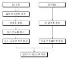
도 1은 본 발명의 유기 전계효과 트랜지스터를 적용한 바이오센서 제조방법을 나타내는 공정도이고, 도 2의 (a) 내지 (j)는 도 1의 공정에 따라 제조되는 바이오센서의 단면을 나타내는 도면이다.1 is a process chart showing a biosensor manufacturing method using the organic field effect transistor of the present invention, Figure 2 (a) to (j) is a view showing a cross section of the biosensor manufactured according to the process of FIG.
도 2의 (a)에 나타난 바와 같이 먼저 제1기판(110)을 준비한다. 제1기판(110)은 플라스틱 또는 글라스 재질의 기판이 가능하며, 폴리이미드(polyimide)를 사용하면 유연성이 뛰어난 바이오센서를 만들 수 있다.As shown in FIG. 2A, first, the
다음으로 도 2의 (b)와 같이 제1기판(110)의 밑면에 절연체 게이트(120)를 증착한다. 절연체(120)는 무기물 산화막이거나, 유기물과 무기물의 적층구조일 수 있으며, 또 유기물과 무기물의 나노복합체일 수도 있다.Next, as illustrated in FIG. 2B, an
이때 증착되는 무기물 산화막은 SiO2, SiOxNy, Si3N4, Al2O3, Ta2O5, Al2O3-ZrO2, Al2O3-Ta2O5, SnO2, ZrO2, PbTiO2, WO3, AlN의 무기물 중에 하나로 이온 민감성 절연체이다. 이 무기물을 증착하는 방법은 화학기상증착법, 물리기상증착법 및 원자층증착법 등을 사용할 수 있다.The inorganic oxide film deposited at this time is SiO2 , SiOx Ny , Si3 N4 , Al2 O3 , Ta2 O5 , Al2 O3 -ZrO2 , Al2 O3 -Ta2 O5 , SnO2 , One of the inorganic materials of ZrO2 , PbTiO2 , WO3 , AlN is an ion sensitive insulator. As the method for depositing the inorganic substance, chemical vapor deposition, physical vapor deposition, atomic layer deposition, or the like can be used.
그리고 유기물과 무기물의 적층구조는 유기물 절연막을 증착한 뒤에 Ta2O5, Al2O3 및 HfO2 박막을 증착하고, 다시 유기물 절연막을 증착하여 형성한다. 이러한 유기물과 무기물의 적층구조를 이용하면 저온에서 높은 품질의 이온 민감성 절연층을 형성할 수 있다. 또 유기물과 무기물의 나노복합체는 나노입자를 유기절연체에 복합화시킨 것으로, 나노입자가 높은 표면적 분율을 갖기 때문에 절연체 게이트(120)의 이온 민감성이 향상되고 저온 액상 공정이 가능하다.The organic and inorganic layered structure is formed by depositing an organic insulating film and then depositing a Ta2 O5 , Al2 O3, and HfO2 thin film, and then depositing an organic insulating film. By using the stacked structure of organic and inorganic materials, it is possible to form a high quality ion sensitive insulating layer at a low temperature. In addition, the nanocomposite of organic and inorganic materials is a composite of nanoparticles in an organic insulator. Since the nanoparticles have a high surface area fraction, ion sensitivity of the
도 2의 (c)는 절연체 게이트(120)가 증착된 제1기판(110)을 식각하여 반응조(300)를 형성한 모습을 나타낸다. 반응조(300)는 감지대상 용액이 고이는 우물형태의 공간으로, 제1기판(110)의 잔류부분이 옆면의 벽을 형성하고 바닥에는 절연체 게이트(120)가 드러나 있다. 제1기판(110)을 식각하는 방법은 노광공정을 포함하는 사진식각공정을 이용할 수 있다.2 (c) shows a state in which the
도 2의 (d)는 절연체 게이트(120) 밑면에 유기 반도체층(130)을 증착한 모습을 나타낸다. 실리콘 기판이 아닌 유기 반도체를 증착하여 유기 전계효과 트랜지스터를 제조하기 때문에 재료비가 매우 저렴하고 생산 공정이 간단해져 전체적인 생산비용을 절감할 수 있다. 또한 증착에 의하기 때문에 넓은 면적의 센서를 만들 수 있고, 유기 반도체의 특성상 유연한 센서를 만들 수 도 있다. 이러한 유기 반도체층(130)에 사용되는 유기 반도체는 n형 올리고머, 또는 p형 올리고머가 사용될 수 있다. p형 올리고머의 예로는 펜타센(pentacene), 다이메틸 펜타센(Me2-pentacene), 비스-벤조디티오펜(bis-benzodithiophene), 비스-티오펜 다이머(bis-thiophene dimer), 섹시티펜(sexithiphene), 헥실 치환 티오펜 올리고머(hexyl-substituted thiophene oligomers), 믹스트 티오펜-페닐렌 올리고머(mixed thiophene-phenylene oligomers), 안트라디티오펜(anthradithiophene), 루벤(rubene), 카퍼 프탈로시아닌(copper phthalocyanine) 등이 있다. 또 n형 올리고머의 예로는 폴리(3-헥실티펜)(poly(3-hexylthiphene)), 폴리쿼터티오펜(polyquarterthiophenes), 폴리[9,9-디옥틸플루오렌-코-바이티오펜](poly[9,9- dioctylfluorene-co-bithiophene]), 9,9-디알킬플루오렌-알트-트리아릴아민(9,9-dialkylfluorene-alt-triarylamine), 카바졸(carbazole), 폴리트릴아릴아민(polytriarylamines) 폴리머 또는 퀴노이메탄 테르티오펜(quinoimethane terthiophene), 퍼플루오로아렌-티오펜 올리고머(perfluoroarene-thiophene oligomers) , 나프탈렌 카르보다이이미드(naphthalene carbodiimide) 단량체, 플러렌(fullerenes) 등이 있다.2 (d) shows a state in which the
도 2의 (e)는 유기 반도체층(130)의 밑면에 소스 전극(140)과 드레인 전극(150)을 형성한 모습을 나타낸다. 유기 전계효과 트랜지스터를 완성하기 위하여 전극(140, 150)을 형성하는 과정이며, 이 전극(140, 150)은 금, 니켈, 알루미늄, 은, 크롬 중에서 선택될 수 있다.FIG. 2E illustrates the
도 2의 (f)는 본 발명의 유기 전계효과 트랜지스터를 이용한 바이오센서의 기준전극을 형성하기 위한 제2기판(210)을 나타낸다. 제2기판(210)도 역시 플라스틱 또는 글라스 재질의 기판이 가능하며, 폴리이미드(polyimide)를 사용하면 유연성이 뛰어난 바이오센서를 만들 수 있다.2 (f) shows a
도 2의 (g)는 제2기판(210)에 기준전극을 형성하기 위한 은 금속층(220)을 증착한 모습을 나타낸다.FIG. 2G illustrates a deposition of a
도 2의 (h)는 제2기판(210)에 미세유동채널벽(230)을 형성한 모습이다. 미세유동채널벽(230)은 미세유동채널이 형성된 부분으로서, 감광성 고분자 또는 실리콘 공중합체를 이용하여 형성할 수 있다. 실리콘 고분자의 일종인 PDMS(polydimethylsiloxane)를 이용할 수 있다.FIG. 2 (h) illustrates the formation of the
도 2의 (i)는 은 금속층(220)을 염소화하여 은/염화은 미세기준 전극(224)을 형성한 모습을 나타낸다. 은 금속층(220)의 표면을 습식 또는 건식 방법을 이용하여 염소화하여 염화은층(222)을 형성하며, 은/염화은 미세기준 전극(224)의 안정성을 위해서 표면을 코팅할 수 있다.FIG. 2 (i) shows the formation of the silver / silver chloride
도 2의 (j)는 제1기판(110)과 제2기판(210)을 접합한 모습을 나타낸다. 이때, 제1기판(110)의 잔류부분과 제2기판(210)에 형성된 미세유동채널벽(220)을 자외선 경화형(UV-curable) 에폭시 또는 열 경화형(thermal-curable) 에폭시를 이용하여 접합한다. 이로써, 내부에 반응조(300)가 형성된 바이오센서가 완성되며, 이러한 구조의 바이오센서는 다수 개의 센서가 집적된 바이오칩을 제작하기 쉽다.2 (j) shows a state in which the
상기 방법의 제조된 유기 전계효과 트랜지스터를 이용한 바이오센서의 작용을 설명하면 다음과 같다.Referring to the operation of the biosensor using the prepared organic field effect transistor of the method as follows.
미세유동채널벽(220)에 형성된 미세유동채널을 통하여 감지대상 물질이 포함된 용액이 반응조(300)에 유입되면, 용액이 접하는 절연체 게이트(120)가 감지대상 이온에 민감하기 때문에 절연체 게이트(120)와 용액 사이의 전기 화학적 전위차가 감지대상 이온의 농도에 따라 변화한다. 이 전위차의 변화는 문턱 전압(VT)의 변화를 가져오며, 문턱 전압의 변화는 유효 게이트 전압(Vgd)의 변화를 유발한다. 이때 발생하는 전계효과에 의해서 컨덕턴스가 게이트 전압에 비례하여 변화한다. 따라서 드레인 전류(Ids)의 변화는 이온 농도의 변화를 타나내므로, 이를 측정하여 이온 농도의 변화를 감지할 수 있는 것이다.When the solution containing the sensing material enters the
다른 측정방법은 다음과 같다. 일정한 드레인 전압(Vds)에서 용액 내의 이온 농도에 변화(ΔCi)가 생기면 일정한 드레인 전류(Ids)를 유지하기 위해서 게이트 전압(Vgs)이 변화한다. 이 게이트 전압의 변화량(ΔVgs)을 측정하여 이온 농도의 변화를 감지할 수 있다.Other measurement methods are as follows. When a change ΔCi occurs in the ion concentration in the solution at a constant drain voltage Vds , the gate voltage Vgs changes to maintain a constant drain current Ids . A change in the ion concentration can be detected by measuring the change amount ΔVgs of the gate voltage.
이때, 절연체 게이트(120)의 종류를 바꾸면 다양한 이온을 검출하는 바이오센서를 제조할 수 있다. 나아가 도 3에 나타낸 바와 같이 절연체 게이트(120)의 표면에 항체(122)를 고정하면, 항원-항체 반응에 따른 드레인 전류의 변화를 측정하여 항원(124)의 밀도를 측정할 수 있다.In this case, by changing the type of the
이상에서는 본 발명을 특정의 바람직한 실시예에 대해서 도시하고 설명하였다. 그러나 본 발명은 상술한 실시예에만 국한되는 것은 아니며, 본 발명이 속하는 기술분야에서 통상의 지식을 가진 자라면 본 발명의 기술적 사상을 벗어남이 없이 얼마든지 다양하게 변경 실시할 수 있을 것이다. 따라서 본 발명의 권리범위는 특정 실시예에 한정되는 것이 아니라, 첨부된 특허청구범위에 의해 정해지는 것으로 해석되어야 할 것이다.In the above, the present invention has been shown and described with respect to certain preferred embodiments. However, the present invention is not limited only to the above-described embodiment, and those skilled in the art to which the present invention pertains can make various changes without departing from the technical spirit of the present invention. Therefore, the scope of the present invention should not be limited to the specific embodiments, but should be construed as defined by the appended claims.
도 1은 본 발명의 유기 전계효과 트랜지스터를 적용한 바이오센서 제조방법을 나타내는 공정도이다.1 is a process chart showing a biosensor manufacturing method to which the organic field effect transistor of the present invention is applied.
도 2는 본 발명의 유기 전계효과 트랜지스터를 적용한 바이오센서의 기본 구조를 나타내는 도면이다.2 is a view showing the basic structure of the biosensor to which the organic field effect transistor of the present invention is applied.
< 도면의 주요부분에 대한 부호의 설명 >Description of the Related Art
110: 제1기판120: 절연체 게이트110: first substrate 120: insulator gate
130: 유기 반도체층140: 소스 전극130: organic semiconductor layer 140: source electrode
150: 드레인 전극210: 제2기판150: drain electrode 210: second substrate
220: 은 금속층224: 은/염화은 미세기준 전극220: silver metal layer 224: silver / silver chloride fine reference electrode
225: 염화은층230: 미세유동채널벽225: silver chloride layer 230: microfluidic channel wall
300: 반응조300: reactor
Claims (15)
Translated fromKoreanPriority Applications (1)
| Application Number | Priority Date | Filing Date | Title |
|---|---|---|---|
| KR1020080057916AKR100987105B1 (en) | 2008-06-19 | 2008-06-19 | Biosensor using organic field effect transistor and its manufacturing method |
Applications Claiming Priority (1)
| Application Number | Priority Date | Filing Date | Title |
|---|---|---|---|
| KR1020080057916AKR100987105B1 (en) | 2008-06-19 | 2008-06-19 | Biosensor using organic field effect transistor and its manufacturing method |
Publications (2)
| Publication Number | Publication Date |
|---|---|
| KR20090131918A KR20090131918A (en) | 2009-12-30 |
| KR100987105B1true KR100987105B1 (en) | 2010-10-11 |
Family
ID=41691037
Family Applications (1)
| Application Number | Title | Priority Date | Filing Date |
|---|---|---|---|
| KR1020080057916AExpired - Fee RelatedKR100987105B1 (en) | 2008-06-19 | 2008-06-19 | Biosensor using organic field effect transistor and its manufacturing method |
Country Status (1)
| Country | Link |
|---|---|
| KR (1) | KR100987105B1 (en) |
Cited By (3)
| Publication number | Priority date | Publication date | Assignee | Title |
|---|---|---|---|---|
| KR101420916B1 (en) | 2012-05-22 | 2014-07-17 | 한양대학교 산학협력단 | Device for cell counting and method for cell counting |
| KR101420917B1 (en) | 2012-05-22 | 2014-08-14 | 한양대학교 산학협력단 | Device for cell counting and method for manufacturing the same |
| KR101484822B1 (en) | 2012-12-07 | 2015-01-21 | 한양대학교 산학협력단 | Device for cell counting and method for manufacturing the same |
Families Citing this family (3)
| Publication number | Priority date | Publication date | Assignee | Title |
|---|---|---|---|---|
| KR101056467B1 (en)* | 2010-03-05 | 2011-08-12 | 한국과학기술원 | Biosensor using field effect transistor and its manufacturing method |
| KR20180057915A (en)* | 2016-11-23 | 2018-05-31 | 주식회사 엘지화학 | Biosensor |
| CN115501920B (en)* | 2022-09-16 | 2024-04-05 | 中国人民解放军陆军特色医学中心 | Preparation method of nucleic acid amplification detection micro-fluidic chip of organic electrochemical crystal Guan Zengmin |
Citations (4)
| Publication number | Priority date | Publication date | Assignee | Title |
|---|---|---|---|---|
| US20060016699A1 (en) | 2004-07-21 | 2006-01-26 | Masao Kamahori | Apparatus and method for measuring biological material |
| JP2006258661A (en) | 2005-03-17 | 2006-09-28 | Canon Inc | Organic transistor biosensor and biosensor measurement method |
| JP2008003058A (en)* | 2006-06-26 | 2008-01-10 | Canon Inc | Dual gate type sensor |
| KR20080027041A (en)* | 2006-09-22 | 2008-03-26 | 삼성전자주식회사 | Nucleic acid length measurement method using FET-based biosensor |
- 2008
- 2008-06-19KRKR1020080057916Apatent/KR100987105B1/ennot_activeExpired - Fee Related
Patent Citations (4)
| Publication number | Priority date | Publication date | Assignee | Title |
|---|---|---|---|---|
| US20060016699A1 (en) | 2004-07-21 | 2006-01-26 | Masao Kamahori | Apparatus and method for measuring biological material |
| JP2006258661A (en) | 2005-03-17 | 2006-09-28 | Canon Inc | Organic transistor biosensor and biosensor measurement method |
| JP2008003058A (en)* | 2006-06-26 | 2008-01-10 | Canon Inc | Dual gate type sensor |
| KR20080027041A (en)* | 2006-09-22 | 2008-03-26 | 삼성전자주식회사 | Nucleic acid length measurement method using FET-based biosensor |
Cited By (3)
| Publication number | Priority date | Publication date | Assignee | Title |
|---|---|---|---|---|
| KR101420916B1 (en) | 2012-05-22 | 2014-07-17 | 한양대학교 산학협력단 | Device for cell counting and method for cell counting |
| KR101420917B1 (en) | 2012-05-22 | 2014-08-14 | 한양대학교 산학협력단 | Device for cell counting and method for manufacturing the same |
| KR101484822B1 (en) | 2012-12-07 | 2015-01-21 | 한양대학교 산학협력단 | Device for cell counting and method for manufacturing the same |
Also Published As
| Publication number | Publication date |
|---|---|
| KR20090131918A (en) | 2009-12-30 |
Similar Documents
| Publication | Publication Date | Title |
|---|---|---|
| Knopfmacher et al. | Nernst limit in dual-gated Si-nanowire FET sensors | |
| KR101359735B1 (en) | Transparent ion detection sensor chip comprising field effect transistor signal transducer with extended gate electrode and preparation method thereof | |
| Vu et al. | Fabrication and application of silicon nanowire transistor arrays for biomolecular detection | |
| KR100987105B1 (en) | Biosensor using organic field effect transistor and its manufacturing method | |
| Tang et al. | Solution processed low power organic field-effect transistor bio-chemical sensor of high transconductance efficiency | |
| EP1085319B1 (en) | A device for detecting an analyte in a sample based on organic materials | |
| KR101257221B1 (en) | Cell based sensor with optical observation of cell capacity by real time, preparation method thereof and multianalyte-detectable sensor chip using the same | |
| CN107449812B (en) | Biochemical sensor under CMOS standard process | |
| Kumar et al. | thin-film transistors (TFTs) for highly sensitive biosensing applications: a review | |
| US20170336347A1 (en) | SiNW PIXELS BASED INVERTING AMPLIFIER | |
| Rashid et al. | Dielectrically modulated label free metal controlled organic thin film transistor for biosensing applications | |
| Soikkeli et al. | Wafer-scale graphene field-effect transistor biosensor arrays with monolithic CMOS readout | |
| Baruah et al. | Numerical assessment of dielectrically-modulated short-double-gate PNPN TFET-based label-free biosensor | |
| Hinnemo et al. | Protein sensing beyond the debye length using graphene field-effect transistors | |
| CN117825474B (en) | A planar extended gate organic field effect transistor and its preparation method and application | |
| Di Lauro et al. | The substrate is a pH-controlled second gate of electrolyte-gated organic field-effect transistor | |
| EP3180606A1 (en) | Electrolyte-gated transistors for detection of molecules | |
| Jain et al. | Dielectric modulated bilayer electrode top contact OTFT for label free biosensing | |
| Lee et al. | CMOS biosensors for the detection of DNA hybridization in high ionic-strength solutions | |
| JP5903872B2 (en) | Transistor type sensor and method for manufacturing transistor type sensor | |
| Vu et al. | Fabrication and application of a microfluidic‐embedded silicon nanowire biosensor chip | |
| Madhavi et al. | Design and analysis of 18 nm multichannel FinFET as biosensor for detection of biological species | |
| Chen et al. | Contacting versus insulated gate electrode for Si nanoribbon field-effect sensors operating in electrolyte | |
| KR101625705B1 (en) | Biosensor using single-electron transistors operating at room temperature, manufacturing method of the biosensor, analysis system having the biosensor and analysis method | |
| Rani et al. | Silicon nanowire field-effect biosensors |
Legal Events
| Date | Code | Title | Description |
|---|---|---|---|
| A201 | Request for examination | ||
| PA0109 | Patent application | St.27 status event code:A-0-1-A10-A12-nap-PA0109 | |
| PA0201 | Request for examination | St.27 status event code:A-1-2-D10-D11-exm-PA0201 | |
| D13-X000 | Search requested | St.27 status event code:A-1-2-D10-D13-srh-X000 | |
| D14-X000 | Search report completed | St.27 status event code:A-1-2-D10-D14-srh-X000 | |
| PG1501 | Laying open of application | St.27 status event code:A-1-1-Q10-Q12-nap-PG1501 | |
| E902 | Notification of reason for refusal | ||
| PE0902 | Notice of grounds for rejection | St.27 status event code:A-1-2-D10-D21-exm-PE0902 | |
| E13-X000 | Pre-grant limitation requested | St.27 status event code:A-2-3-E10-E13-lim-X000 | |
| P11-X000 | Amendment of application requested | St.27 status event code:A-2-2-P10-P11-nap-X000 | |
| P13-X000 | Application amended | St.27 status event code:A-2-2-P10-P13-nap-X000 | |
| E701 | Decision to grant or registration of patent right | ||
| PE0701 | Decision of registration | St.27 status event code:A-1-2-D10-D22-exm-PE0701 | |
| GRNT | Written decision to grant | ||
| PR0701 | Registration of establishment | St.27 status event code:A-2-4-F10-F11-exm-PR0701 | |
| PR1002 | Payment of registration fee | Fee payment year number:1 St.27 status event code:A-2-2-U10-U11-oth-PR1002 | |
| P14-X000 | Amendment of ip right document requested | St.27 status event code:A-5-5-P10-P14-nap-X000 | |
| PG1601 | Publication of registration | St.27 status event code:A-4-4-Q10-Q13-nap-PG1601 | |
| P16-X000 | Ip right document amended | St.27 status event code:A-5-5-P10-P16-nap-X000 | |
| Q16-X000 | A copy of ip right certificate issued | St.27 status event code:A-4-4-Q10-Q16-nap-X000 | |
| PN2301 | Change of applicant | St.27 status event code:A-5-5-R10-R11-asn-PN2301 St.27 status event code:A-5-5-R10-R13-asn-PN2301 | |
| PN2301 | Change of applicant | St.27 status event code:A-5-5-R10-R11-asn-PN2301 St.27 status event code:A-5-5-R10-R13-asn-PN2301 | |
| R18-X000 | Changes to party contact information recorded | St.27 status event code:A-5-5-R10-R18-oth-X000 | |
| FPAY | Annual fee payment | Payment date:20130930 Year of fee payment:4 | |
| PR1001 | Payment of annual fee | Fee payment year number:4 St.27 status event code:A-4-4-U10-U11-oth-PR1001 | |
| FPAY | Annual fee payment | Payment date:20140923 Year of fee payment:5 | |
| PR1001 | Payment of annual fee | Fee payment year number:5 St.27 status event code:A-4-4-U10-U11-oth-PR1001 | |
| LAPS | Lapse due to unpaid annual fee | ||
| PC1903 | Unpaid annual fee | Not in force date:20151006 Payment event data comment text:Termination Category : DEFAULT_OF_REGISTRATION_FEE St.27 status event code:A-4-4-U10-U13-oth-PC1903 | |
| R18-X000 | Changes to party contact information recorded | St.27 status event code:A-5-5-R10-R18-oth-X000 | |
| P22-X000 | Classification modified | St.27 status event code:A-4-4-P10-P22-nap-X000 | |
| PC1903 | Unpaid annual fee | Ip right cessation event data comment text:Termination Category : DEFAULT_OF_REGISTRATION_FEE Not in force date:20151006 St.27 status event code:N-4-6-H10-H13-oth-PC1903 | |
| R18-X000 | Changes to party contact information recorded | St.27 status event code:A-5-5-R10-R18-oth-X000 | |
| R18-X000 | Changes to party contact information recorded | St.27 status event code:A-5-5-R10-R18-oth-X000 | |
| PN2301 | Change of applicant | St.27 status event code:A-5-5-R10-R11-asn-PN2301 St.27 status event code:A-5-5-R10-R13-asn-PN2301 | |
| P22-X000 | Classification modified | St.27 status event code:A-4-4-P10-P22-nap-X000 | |
| R18-X000 | Changes to party contact information recorded | St.27 status event code:A-5-5-R10-R18-oth-X000 |