KR100985184B1 - Electrical element and its formation method - Google Patents
Electrical element and its formation methodDownload PDFInfo
- Publication number
- KR100985184B1 KR100985184B1KR1020080071755AKR20080071755AKR100985184B1KR 100985184 B1KR100985184 B1KR 100985184B1KR 1020080071755 AKR1020080071755 AKR 1020080071755AKR 20080071755 AKR20080071755 AKR 20080071755AKR 100985184 B1KR100985184 B1KR 100985184B1
- Authority
- KR
- South Korea
- Prior art keywords
- phase change
- change pattern
- fuse
- cell
- region
- Prior art date
- Legal status (The legal status is an assumption and is not a legal conclusion. Google has not performed a legal analysis and makes no representation as to the accuracy of the status listed.)
- Active
Links
Images


Classifications
- H—ELECTRICITY
- H10—SEMICONDUCTOR DEVICES; ELECTRIC SOLID-STATE DEVICES NOT OTHERWISE PROVIDED FOR
- H10N—ELECTRIC SOLID-STATE DEVICES NOT OTHERWISE PROVIDED FOR
- H10N70/00—Solid-state devices having no potential barriers, and specially adapted for rectifying, amplifying, oscillating or switching
- H10N70/20—Multistable switching devices, e.g. memristors
- H10N70/231—Multistable switching devices, e.g. memristors based on solid-state phase change, e.g. between amorphous and crystalline phases, Ovshinsky effect
- H—ELECTRICITY
- H10—SEMICONDUCTOR DEVICES; ELECTRIC SOLID-STATE DEVICES NOT OTHERWISE PROVIDED FOR
- H10B—ELECTRONIC MEMORY DEVICES
- H10B63/00—Resistance change memory devices, e.g. resistive RAM [ReRAM] devices
- H10B63/80—Arrangements comprising multiple bistable or multi-stable switching components of the same type on a plane parallel to the substrate, e.g. cross-point arrays
- H—ELECTRICITY
- H10—SEMICONDUCTOR DEVICES; ELECTRIC SOLID-STATE DEVICES NOT OTHERWISE PROVIDED FOR
- H10N—ELECTRIC SOLID-STATE DEVICES NOT OTHERWISE PROVIDED FOR
- H10N70/00—Solid-state devices having no potential barriers, and specially adapted for rectifying, amplifying, oscillating or switching
- H10N70/011—Manufacture or treatment of multistable switching devices
- H10N70/061—Shaping switching materials
- H10N70/066—Shaping switching materials by filling of openings, e.g. damascene method
- H—ELECTRICITY
- H10—SEMICONDUCTOR DEVICES; ELECTRIC SOLID-STATE DEVICES NOT OTHERWISE PROVIDED FOR
- H10N—ELECTRIC SOLID-STATE DEVICES NOT OTHERWISE PROVIDED FOR
- H10N70/00—Solid-state devices having no potential barriers, and specially adapted for rectifying, amplifying, oscillating or switching
- H10N70/011—Manufacture or treatment of multistable switching devices
- H10N70/061—Shaping switching materials
- H10N70/068—Shaping switching materials by processes specially adapted for achieving sub-lithographic dimensions, e.g. using spacers
- H—ELECTRICITY
- H10—SEMICONDUCTOR DEVICES; ELECTRIC SOLID-STATE DEVICES NOT OTHERWISE PROVIDED FOR
- H10N—ELECTRIC SOLID-STATE DEVICES NOT OTHERWISE PROVIDED FOR
- H10N70/00—Solid-state devices having no potential barriers, and specially adapted for rectifying, amplifying, oscillating or switching
- H10N70/801—Constructional details of multistable switching devices
- H10N70/821—Device geometry
- H10N70/826—Device geometry adapted for essentially vertical current flow, e.g. sandwich or pillar type devices
- H—ELECTRICITY
- H10—SEMICONDUCTOR DEVICES; ELECTRIC SOLID-STATE DEVICES NOT OTHERWISE PROVIDED FOR
- H10N—ELECTRIC SOLID-STATE DEVICES NOT OTHERWISE PROVIDED FOR
- H10N70/00—Solid-state devices having no potential barriers, and specially adapted for rectifying, amplifying, oscillating or switching
- H10N70/801—Constructional details of multistable switching devices
- H10N70/841—Electrodes
- H10N70/8413—Electrodes adapted for resistive heating
- H—ELECTRICITY
- H10—SEMICONDUCTOR DEVICES; ELECTRIC SOLID-STATE DEVICES NOT OTHERWISE PROVIDED FOR
- H10N—ELECTRIC SOLID-STATE DEVICES NOT OTHERWISE PROVIDED FOR
- H10N70/00—Solid-state devices having no potential barriers, and specially adapted for rectifying, amplifying, oscillating or switching
- H10N70/801—Constructional details of multistable switching devices
- H10N70/881—Switching materials
- H10N70/882—Compounds of sulfur, selenium or tellurium, e.g. chalcogenides
- H10N70/8825—Selenides, e.g. GeSe
- H—ELECTRICITY
- H10—SEMICONDUCTOR DEVICES; ELECTRIC SOLID-STATE DEVICES NOT OTHERWISE PROVIDED FOR
- H10N—ELECTRIC SOLID-STATE DEVICES NOT OTHERWISE PROVIDED FOR
- H10N70/00—Solid-state devices having no potential barriers, and specially adapted for rectifying, amplifying, oscillating or switching
- H10N70/801—Constructional details of multistable switching devices
- H10N70/881—Switching materials
- H10N70/882—Compounds of sulfur, selenium or tellurium, e.g. chalcogenides
- H10N70/8828—Tellurides, e.g. GeSbTe
Landscapes
- Engineering & Computer Science (AREA)
- Manufacturing & Machinery (AREA)
- Semiconductor Memories (AREA)
Abstract
Translated fromKorean
Description
Translated fromKorean본 발명은 전기 소자에 관한 것이며, 더 구체적으로, 상 변화 퓨즈 소자 및 상변화 기억 소자에 관한 것이다.The present invention relates to an electrical element, and more particularly, to a phase change fuse element and a phase change memory element.
이동 통신 및 컴퓨터 등과 같은 전자 산업의 발전에 따라, 빠른 읽기/쓰기 동작 속도, 비휘발성 및 낮은 동작 전압 등의 특성을 갖는 반도체 장치가 요구되고 있다. 하지만, 현재 사용되는 에스램(static random access memory; SRAM), 디램(Dynamic Random Access Memory; DRAM) 및 플래쉬 메모리(FLASH memory) 등과 같은 메모리 장치는 이러한 특성들을 모두 충족시키지 못하고 있다. 예를 들면, 상기 디램의 단위 셀은 한 개의 커패시터와 이를 제어하기 위한 한 개의 트랜지스터를 구비하기 때문에, 낸드 플래시 메모리에 비해 상대적으로 큰 단위 셀 면적을 갖는다. 디램은 커패시터에 정보를 저장하기 때문에, 알려진 것처럼, 리프레시 동작이 필요한 휘발성 메모리 장치이다. 상기 에스램은 빠른 동작 속도를 갖지만, 휘발성 메모리 장치의 하나이며, 특히 단위 셀은 여섯 개의 트랜지스터들로 구성되기 때문에 단위 셀 면적이 매우 큰 단점을 갖는다. 상기 플래시 메모리는 비휘발성 메모리 장치이면서, (특히 낸드형 플래시 메모리 장치의 경우) 현존하는 메모리 장치들 중의 가장 높은 집적도를 제공하지만, 알려진 것처럼 동작 속도가 느린 단점을 갖는다.BACKGROUND With the development of the electronics industry such as mobile communication and computers, semiconductor devices having characteristics such as high read / write operation speed, nonvolatile and low operating voltage are required. However, currently used memory devices such as static random access memory (SRAM), dynamic random access memory (DRAM), and flash memory do not meet all of these characteristics. For example, since the unit cell of the DRAM includes one capacitor and one transistor for controlling the DRAM, the unit cell has a relatively large unit cell area compared to the NAND flash memory. DRAMs are volatile memory devices that require refresh operations, as they are known, because they store information in capacitors. The SRAM has a high operating speed, but is one of volatile memory devices. In particular, the SRAM has a large unit cell area because the unit cell is composed of six transistors. The flash memory is a nonvolatile memory device and provides the highest degree of integration among existing memory devices (particularly in the case of NAND flash memory devices), but has the disadvantage of slow operation speed as is known.
이에 따라, 최근에는 빠른 읽기/쓰기 동작이 가능하며, 비휘발성을 갖고, 리프레쉬 동작이 불필요하며, 동작 전압이 낮은 메모리 장치에 대한 연구가 진행되고 있으며, 상변화 랜덤 억세스 메모리(phase random access memory; PRAM)는 이러한 기술적 요구들을 충족시킬 수 있을 것으로 기대되는 차세대 메모리 장치의 한가지이다. 예를 들면, PRAM은 대략 1013회 이상의 정보 변경이 가능하기 때문에 제품 수명이 길며, 대략 30ns의 고속 동작이 가능한 장점을 아울러 갖는다.Accordingly, in recent years, research has been conducted on memory devices capable of fast read / write operations, nonvolatile, refresh operations, and low operating voltages, and include phase random access memory; PRAM) is one of the next generation memory devices that are expected to meet these technical requirements. For example, a PRAM can change information more than 10 to13 times, so it has a long product life and has a high speed of about 30 ns.
PRAM의 상변화 패턴은 서로 구별 가능한 적어도 두 상태, 예컨대 결정질 상태, 비정질 상태 그리고 이들 사이의 적어도 하나 이상의 중간 상태들을 나타낼 수 있어 메모리 요소로 사용될 수 있다. 비정질 상태는 결정질 상태보다 상대적으로 높은 비저항을 나타내며, 중간상태들은 비정질 상태 및 결정질 상태 사이의 비저항을 나타낸다.The phase change pattern of the PRAM may represent at least two distinguishable states, such as a crystalline state, an amorphous state, and at least one or more intermediate states therebetween, and thus may be used as memory elements. Amorphous states exhibit a relatively higher resistivity than crystalline states, and intermediate states exhibit a resistivity between an amorphous state and a crystalline state.
본 발명이 해결하고자 하는 일 기술적 과제는 프로 그램 가능하면서 서로 다른 열적 특성 가진 셀 상변화 소자 및 퓨즈 상변화 소자를 제공하는 것이다.One technical problem to be solved by the present invention is to provide a cell phase change device and a fuse phase change device that can be programmed and have different thermal characteristics.
본 발명이 해결하고자 하는 일 기술적 과제는 프로 그램 가능하면서 서로 다른 열적 특성 가진 셀 상변화 소자 및 퓨즈 상변화 소자의 형성 방법을 제공하는 것이다. One technical problem to be solved by the present invention is to provide a method for forming a cell phase change device and a fuse phase change device that are programmable and have different thermal characteristics.
본 발명의 일 실시예에 따른 전기 소자는 기판에 형성된 하부 배선, 상기 하부 배선 상에 형성된 제1 상변화 패턴, 상기 제1 상변화 패턴 상에 형성된 제2 상변화 패턴, 및 상기 상변화 패턴 상에 형성된 상부 배선을 포함하되, 상기 제1 상변화 패턴의 결정화 온도는 상기 제2 상변화 패턴의 결정화 온도보다 높다.An electrical device according to an embodiment of the present invention includes a lower wiring formed on a substrate, a first phase change pattern formed on the lower wiring, a second phase change pattern formed on the first phase change pattern, and the phase change pattern phase Including an upper wiring formed in, the crystallization temperature of the first phase change pattern is higher than the crystallization temperature of the second phase change pattern.
본 발명의 일 실시예에 있어서, 상기 하부 배선과 상기 제1 상변화 패턴 사이에 개재된 하부 전극을 더 포함할 수 있다.In one embodiment of the present invention, the lower electrode may further include a lower electrode interposed between the first phase change pattern.
본 발명의 일 실시예에 있어서, 상기 하부 전극의 측면에 배치된 스페이서를 더 포함할 수 있다.In one embodiment of the present invention, it may further include a spacer disposed on the side of the lower electrode.
본 발명의 일 실시예에 있어서, 상기 제2 상변화 패턴과 상기 상부 배선 사이에 개재된 상부 전극을 더 포함할 수 있다.In one embodiment of the present invention, it may further include an upper electrode interposed between the second phase change pattern and the upper wiring.
본 발명의 일 실시예에 있어서, 상기 상부 전극과 상기 상부 배선 사이에 배치된 상부 콘택 플러그를 더 포함할 수 있다.In one embodiment of the present invention, it may further include an upper contact plug disposed between the upper electrode and the upper wiring.
본 발명의 일 실시예에 있어서, 상기 제1 상변화 패턴은 항아리 형태 또는 오목 요철을 가지는 라인 형태이고, 상기 제2 상변화 패턴은 상기 제1 상변화 패턴의 내부에 배치된 항아리 형태 또는 오목 요철을 가지는 라인 형태 이고, 상기 상부 전극은 상기 제2 상변화 패턴의 내부를 채우는 형상을 가질 수 있다.In one embodiment of the present invention, the first phase change pattern is a jar shape or a line shape having concave irregularities, the second phase change pattern is a jar shape or concave irregularities disposed inside the first phase change pattern The upper electrode may have a shape that fills the inside of the second phase change pattern.
본 발명의 일 실시예에 있어서, 상기 제1 상변화 패턴과 상기 제2 상변화 패 턴의 측면은 서로 정렬될 수 있다.In one embodiment of the present invention, side surfaces of the first phase change pattern and the second phase change pattern may be aligned with each other.
본 발명의 일 실시예에 있어서, 상기 제1 상변화 패턴은 항아리 형태 또는 오목 요철을 가지는 라인 형태이고, 상기 제2 상변화 패턴은 상기 제1 상변화 패턴의 내부를 채우는 형상을 가질 수 있다.In one embodiment of the present invention, the first phase change pattern may have a shape of a jar or a line having concave-convex irregularities, and the second phase change pattern may have a shape filling the inside of the first phase change pattern.
본 발명의 일 실시예에 있어서, 상기 제1 상변화 패턴의 측면에 스페이서를 더 포함할 수 있다.In one embodiment of the present invention, the spacer may further include a side surface of the first phase change pattern.
본 발명의 일 실시예에 있어서, 상기 제1 상변화 패턴의 결정화 온도는 섭씨 300 도 이상일 수 있다.In one embodiment of the present invention, the crystallization temperature of the first phase change pattern may be 300 degrees Celsius or more.
본 발명의 일 실시예에 있어서, 상기 제1 상변화 패턴은 InSbTe이고 상기 제2 상변화 패턴은 GeSbTe일 수 있다.In one embodiment of the present invention, the first phase change pattern may be InSbTe and the second phase change pattern may be GeSbTe.
본 발명의 일 실시예에 따른 전기 소자는 퓨즈 영역 및 셀 영역이 구비된 기판, 상기 퓨즈 영역의 상기 기판 상에 형성된 퓨즈 하부 배선, 상기 퓨즈 하부 배선 상에 형성된 퓨즈 상변화 패턴, 및 상기 퓨즈 상변화 패턴 상에 형성된 퓨즈 상부 배선을 포함하는 퓨즈 상변화 소자, 및 상기 셀 영역의 상기 기판 상에 형성된 셀 하부 배선, 상기 셀 하부 배선 상에 형성된 셀 상변화 패턴, 및 상기 셀 상변화 패턴 상에 형성된 셀 상부 배선을 포함하는 셀 상변화 소자를 포함하고, 상기 퓨즈 상변화 패턴의 결정화 온도는 상기 셀 상변화 패턴의 결정화 온도보다 높다.An electrical device according to an embodiment of the present invention is a substrate having a fuse region and a cell region, a fuse lower wiring formed on the substrate of the fuse region, a fuse phase change pattern formed on the fuse lower wiring, and the fuse phase A fuse phase change element including a fuse upper wiring formed on the change pattern, a cell lower wiring formed on the substrate of the cell region, a cell phase change pattern formed on the cell lower wiring, and a cell phase change pattern And a cell phase change element including a formed cell upper wiring, wherein the crystallization temperature of the fuse phase change pattern is higher than the crystallization temperature of the cell phase change pattern.
본 발명의 일 실시예에 있어서, 상기 퓨즈 상변화 패턴은 제1 퓨즈 상변화 패턴 및 제2 퓨즈 상변화 패턴을 포함하고, 상기 제1 퓨즈 상변화 패턴의 결정화 온도는 상기 제2 퓨즈 상변화 패턴의 결정화 온도보다 높을 수 있다.The fuse phase change pattern may include a first fuse phase change pattern and a second fuse phase change pattern, and the crystallization temperature of the first fuse phase change pattern may correspond to the second fuse phase change pattern. It may be higher than the crystallization temperature of.
본 발명의 일 실시예에 있어서, 상기 제2 퓨즈 상변화 패턴과 상기 셀 상변화 패턴은 같은 물질일 수 있다.In one embodiment of the present invention, the second fuse phase change pattern and the cell phase change pattern may be the same material.
본 발명의 일 실시예에 있어서, 상기 제1 퓨즈 상변화 패턴과 상기 제2 퓨즈 상변화 패턴의 측면은 서로 정렬될 수 있다.In an embodiment of the present disclosure, side surfaces of the first fuse phase change pattern and the second fuse phase change pattern may be aligned with each other.
본 발명의 일 실시예에 있어서, 상기 제1 퓨즈 상변화 패턴은 항아리 형태 또는 오목 요철을 가지는 라인 형태이고, 상기 제2 퓨즈 상변화 패턴은 상기 제1 퓨즈 상변화 패턴의 내부를 채우는 형상을 가질 수 있다.In one embodiment of the present invention, the first fuse phase change pattern is a line shape having a jar shape or concave irregularities, the second fuse phase change pattern has a shape to fill the inside of the first fuse phase change pattern. Can be.
본 발명의 일 실시예에 있어서, 상기 퓨즈 상변화 소자 및 상기 셀 상변화 소자는 각각 퓨즈 상부 전극, 및 셀 상부 전극을 더 포함하고, 상기 제1 퓨즈 상변화 패턴은 항아리 형태 또는 오목 요철을 가지는 라인 형태이고, 상기 제2 퓨즈 상변화 패턴은 상기 제1 퓨즈 상변화 패턴의 내부에 배치된 항아리 형태 또는 오목 요철을 가지는 라인 형태이고, 상기 퓨즈 상부 전극은 상기 제2 퓨즈 상변화 패턴의 내부를 채우는 형상을 가지고, 상기 셀 상변화 패턴은 항아리 형태이고, 상기 셀 상부 전극은 상기 셀 상변화 패턴의 내부를 채우는 형상을 가질 수 있다.In an embodiment, the fuse phase change element and the cell phase change element each further include a fuse upper electrode and a cell upper electrode, and the first fuse phase change pattern has a jar shape or concave irregularities. The second fuse phase change pattern is a line shape, and the second fuse phase change pattern is a line shape having a jar shape or concave irregularities disposed inside the first fuse phase change pattern, the fuse upper electrode is the inside of the second fuse phase change pattern The cell phase change pattern may have a shape of a jar, and the cell upper electrode may have a shape that fills the inside of the cell phase change pattern.
본 발명의 일 실시예에 따른 전기 소자의 형성 방법은 기판에 하부 배선을 형성하는 단계, 상기 하부 배선 상에 제1 상변화 패턴 및 제2 상변화 패턴을 형성하는 단계, 및 상기 상변화 패턴 상에 상부 배선을 형성하는 단계를 포함하되, 상기 제1 상변화 패턴의 결정화 온도는 상기 제2 상변화 패턴의 결정화 온도보다 높다.According to an embodiment of the present invention, a method of forming an electrical device includes forming a lower wiring on a substrate, forming a first phase change pattern and a second phase change pattern on the lower wiring, and the phase change pattern phase. And forming an upper wiring in the semiconductor device, wherein the crystallization temperature of the first phase change pattern is higher than the crystallization temperature of the second phase change pattern.
본 발명의 일 실시예에 있어서, 상기 제1 상변화 패턴의 결정화 온도는 섭씨 300 도 이상일 수 있다.In one embodiment of the present invention, the crystallization temperature of the first phase change pattern may be 300 degrees Celsius or more.
본 발명의 일 실시예에 있어서, 상기 하부 배선과 상기 제1 상변화 패턴 사이에 하부 전극을 형성하는 단계를 더 포함할 수 있다.In an exemplary embodiment, the method may further include forming a lower electrode between the lower wiring and the first phase change pattern.
본 발명의 실시예들에 따른 퓨즈 상변화 소자 및 셀 상변화 소자가 다른 열적 특성을 가지고 있어, 고온의 실장 공정에서 상기 퓨즈 상변화 소자의 프로그램 상태가 변하지 않을 수 있다.Since the fuse phase change device and the cell phase change device according to embodiments of the present invention have different thermal characteristics, the program state of the fuse phase change device may not change in a high temperature mounting process.
PRAM은 칼코게나이드 물질 계열을 사용할 수 있다. 집적도의 증가에 따라 불량의 발생 빈도가 증가할 수 있다. 상기 불량에 따른 수율 저하(yield reduction)를 향상시키기 위하여 PRAM은 리던던시 구조(redundancy structure)를 채용할 수 있다. 상기 리던던시 구조를 적용함에 있어서, 통상적으로 퓨즈 소자가 사용될 수 있다. 상기 퓨즈 소자는 레이저를 이용한 물리적 절단 방법(physical cutting ), 또는 전류를 이용한 전기적 절단 방법(electrical cutting)을 이용할 수 있다. 상기 물리적 절단 방법(physical cutting )은 집적도의 증가에 따라 퓨즈 박스의 면적 및 공정 단계가 증가할 수 있다. 본 발명의 실시예들에 따른 퓨즈 상변화 소자가 퓨즈 소자에 사용될 수 있다. 상기 퓨즈 상변화 소자는 프로그램이 가능하고, 실장(packaging) 후에 불량이 발생하더라도 반복하여 수리(repair)할 수 있다. 한편, PRAM의 실장 공정은 통상적으로 적외선 리플로우(Infra-red reflow: 적외선 리플로우)을 이용할 수 있다. 상기 적외선 리플로우 공정은 섭씨 220도 내지 270도의 온도에서 수행될 수 있다. 따라서, 상기 퓨즈 상변화 소자는 상기 적외선 리플로우 공정에서 상변화가 일어나지 않아야 한다. 셀 상변화 소자와 상기 퓨즈 상변화 소자의 온도 특성은 각각 다를 수 있다. 상기 셀 상변화 소자의 상변화 패턴은 GeSbTe(GST) 물질 등으로 형성하고, 상기 퓨즈 소자의 상변화 패턴은 결정화 온도가 상기 GST 물질보다 높은 InSbTe물질로 선택할 수 있다.PRAM may use a family of chalcogenide materials. As the degree of integration increases, the frequency of occurrence of defects may increase. In order to improve yield reduction due to the failure, the PRAM may adopt a redundancy structure. In applying the redundancy structure, a fuse device may be used. The fuse device may use a physical cutting method using a laser or an electrical cutting method using a current. In the physical cutting method, an area of a fuse box and a process step may increase as the degree of integration increases. A fuse phase change element according to embodiments of the present invention may be used in a fuse element. The fuse phase change element is programmable and can be repaired repeatedly even if a defect occurs after packaging. On the other hand, the mounting process of the PRAM can typically use Infra-red reflow (infrared reflow). The infrared reflow process may be performed at a temperature of 220 degrees Celsius to 270 degrees Celsius. Therefore, the fuse phase change element should not cause a phase change in the infrared reflow process. The temperature characteristics of the cell phase change element and the fuse phase change element may be different. The phase change pattern of the cell phase change device may be formed of a GeSbTe (GST) material or the like, and the phase change pattern of the fuse device may be selected as an InSbTe material having a higher crystallization temperature than the GST material.
이하, 첨부한 도면들을 참조하여 본 발명의 바람직한 실시예들을 상세히 설명하기로 한다. 그러나, 본 발명은 여기서 설명되어지는 실시예들에 한정되지 않고 다른 형태로 구체화될 수도 있다. 오히려, 여기서 소개되는 실시예는 개시된 내용이 철저하고 완전해질 수 있도록 그리고 당업자에게 본 발명의 사상이 충분히 전달될 수 있도록 하기 위해 제공되어지는 것이다. 도면들에 있어서, 층 및 영역들의 두께는 명확성을 기하기 위하여 과장되어진 것이다. 또한, 층이 다른 층 또는 기판 "상"에 있다고 언급되어지는 경우에 그것은 다른 층 또는 기판 상에 직접 형성될 수 있거나 또는 그들 사이에 제3의 층이 개재될 수도 있다. 명세서 전체에 걸쳐서 동일한 참조번호로 표시된 부분들은 동일한 구성요소들을 나타낸다.Hereinafter, exemplary embodiments of the present invention will be described in detail with reference to the accompanying drawings. However, the present invention is not limited to the embodiments described herein and may be embodied in other forms. Rather, the embodiments introduced herein are provided so that the disclosure may be made thorough and complete, and to fully convey the spirit of the invention to those skilled in the art. In the drawings, the thicknesses of the layers and regions are exaggerated for clarity. In addition, where a layer is said to be "on" another layer or substrate, it may be formed directly on the other layer or substrate, or a third layer may be interposed therebetween. Portions denoted by like reference numerals denote like elements throughout the specification.
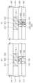
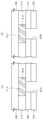
도 1은 본 발명의 일 실시예에 따른 전기 소자를 설명하는 단면도이다.1 is a cross-sectional view illustrating an electrical device according to an embodiment of the present invention.
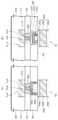
도 1를 참조하면, 기판(100)은 셀 영역(A)과 퓨즈 영역(B)을 포함할 수 있다. 퓨즈 상변화 소자(10f)는 상기 퓨즈 영역(B)에 배치되고, 셀 상변화 소자(10c)는 상기 셀 영역(A)에 배치될 수 있다. 상기 퓨즈 상변화 소자(10f)는 상기 퓨즈 영역(B)에 형성된 퓨즈 하부 배선(112f), 상기 퓨즈 하부 배선(112f) 상에 형성된 퓨즈 상변화 패턴(130f), 및 상기 퓨즈 상변화 패턴(130f) 상에 형성된 퓨즈 상부 배선(160f)을 포함할 수 있다. 상기 셀 상변화 소자(10c)는 상기 셀 영역(A)에 형성된 셀 하부 배선(112c), 상기 셀 하부 배선(112c) 상에 형성된 셀 상변화 패턴(130c), 및 상기 셀 상변화 패턴(130c) 상에 형성된 셀 상부 배선(160c)을 포함할 수 있다. 상기 퓨즈 상변화 패턴(130f)의 결정화 온도는 상기 셀 상변화 패턴(130c)의 결정화 온도보다 높을 수 있다.Referring to FIG. 1, the
상기 기판(100)은 반도체 기판 또는 유전체 기판일 수 있다. 상기 기판(100)은 실리콘 기판, 게르마늄 기판, SOI 기판 중에서 적어도 하나를 포함할 수 있다. 상기 기판(100)은 셀 영역(A)과 퓨즈 영역(B)을 포함할 수 있다. 상기 기판(100)은 하부 구조물(미도시)을 포함할 수 있다. 상기 하부 구조물은 다이오드 또는 트랜지스터를 포함할 수 있다. 상기 기판(100) 상에 하부 층간 절연막(110)이 배치될 수 있다. 상기 하부 층간 절연막(110)은 실리콘 산화막으로 형성될 수 있다. 상기 하부 층간 절연막(110)을 관통하는 하부 콘택홀(114c,114f) 내에 하부 배선(112c,112f)이 배치될 수 있다. 상기 하부 배선(112c,112f)은 도전성 패드를 포함할 수 있다. 상기 하부 배선(112c,112f)은 금속, 금속화합물, 도핑된 반도체 중에서 적어도 하나를 포함할 수 있다. 상기 하부 배선(112c,112f)은 상기 셀 영역(A)에 형성된 셀 하부 배선(112c), 및 상기 퓨즈 영역(B)에 형성된 퓨즈 하부 배선(112f)을 포함할 수 있다. 상기 하부 배선(112c,112f)은 상기 하부 구조물과 전기적으로 연결될 수 있다. 상기 하부 배선(112c,112f)의 상부면과 상기 하부 층간 절연막(110)의 상부면은 같은 높이일 수 있다.The
상기 하부 배선(112c,112f) 및/또는 상기 하부 층간 절연막(110) 상에 중간 층간 절연막(120)이 배치될 수 있다. 상기 중간 층간 절연막(120)을 관통하여 상기 하부 배선(112c,112f)을 노출하는 중간 콘택홀(126c,126f)이 배치될 수 있다. 상기 중간 콘택 홀(126c,126f)은 상기 셀 영역(A)에 형성된 셀 중간 콘택홀(126c) 및 상기 퓨즈 영역(B)에 형성된 퓨즈 중간 콘택홀(126f)을 포함할 수 있다. 상기 중간 층간 절연막(120)은 실리콘산화막일 수 있다.An intermediate
상기 중간 콘택홀(126c,126f)의 측벽에 하부 전극 스페이서(122c,122f)가 배치될 수 있다. 상기 하부 전극 스페이서(122c,122f)는 실리콘질화막 또는 실리콘산화질화막을 포함할 수 있다. 상기 하부 전극 스페이서(122c,122f)는 상기 셀 영역(A)에 형성된 셀 하부 전극 스페이서(122c) 및 상기 퓨즈 영역(B)에 형성된 퓨즈 하부 전극 스페이서(122f)를 포함할 수 있다. 상기 하부 전극 스페이서(122c,122f)의 열 전도도(thermal conductivity)는 상기 중간 층간 절연막(120)의 열 전도도보다 낮을 수 있다.
하부 전극(124c,124f)은 상기 중간 콘택홀(126c,126f) 내에 배치될 수 있다. 상기 하부 전극(124c,124f)은 상기 상변화 패턴(130c,130f)을 가열하는 수단일 수 있다. 상기 하부 전극(124c,124f)은 상기 셀 영역(A)에 형성된 셀 하부 전극(124c) 및 상기 퓨즈 영역(B)에 형성된 퓨즈 하부 전극(124f)을 포함할 수 있다. 상기 하부 전극(124c,124f)은 금속 질화물, 금속, 금속 산화질화물, 실리사이드, 도전성 카본 중에서 적어도 하나를 포함할 수 있다. 구체적으로, 상기 하부 전극(124c,124f)은 Ti, Ta, Mo,W, TiN,TaN,WN,MoN, NbN, TiSiN, TiAlN, TiBN, ZrSiN, WSiN,WBN, ZrAlN, MoSiN, TaSiN, TaAlN, TiW,TiSi,TaSi, TiON, TiAlON, WON, TaON 중에서 적어도 하나를 포함할 수 있다. 상기 하부 전극(124c,124f)의 단면적은 상기 상변화 패턴(130c,130f)의 단면적보다 작을 수 있다. 상기 하부 전극(124c,124f)의 크기의 감소는 접촉 면적을 감소시키어 접촉저항을 증가시킬 수 있다. 따라서, 상기 접촉저항이 큰 경우, 낮은 파워에서 상기 하부 전극(124c,124f)을 높은 온도로 올릴 수 있다. 상기 셀 하부 배선(112c)은 상기 셀 하부 전극(124c)과 전기적으로 연결될 수 있다. 상기 퓨즈 하부 배선(112f)은 상기 퓨즈 하부 전극(124f)과 전기적으로 연결될 수 있다.
상기 상변화 패턴(130c,130f)이 상기 하부 전극(124c,124f) 상에 배치될 수 있다. 상기 상변화 패턴(130c,130f)은 상기 셀 영역(A)에 형성된 셀 상변화 패턴(130c)과 상기 퓨즈 영역(B)에 형성된 퓨즈 상변화 패턴(130f)을 포함할 수 있다. 상기 상변화 패턴(130c,130f)은 상기 상부 배선(160c,160f)과 평행하게 연장될 수 있다.The
본 발명의 변형된 실시예에 따르면, 상기 상변화 패턴(130c,130f)은 아이랜드(island) 형태, 콘택 플러그(contact plug) 형태, 라인(line) 형태 중에서 하나일 수 있다. 상기 상변화 패턴(130c,130f)의 형태는 다양하게 변형될 수 있다.According to a modified embodiment of the present invention, the
상기 셀 영역(A)의 상기 셀 상변화 패턴(130c)은 Ge-Sb-Te, Sb-Te, As-Sb-Te, Sb-Se 중에서 적어도 하나를 포함할 수 있다. 구체적으로, 상기 셀 상변화 패턴(130c)은 Ge2Sb2Te5일 수 있다. 상기 셀 상변화 패턴(130c)은 As-Sb-Te-금속 화합물, As-Ge-Sb-Te-금속 화합물, 금속-Sb-Te-금속 화합물, 5A족 원소-Sb-Te-금속 화합물, 6A족 원소-Sb-Te-금속 화합물, 5A족 원소-Sb-Se-금속 화합물, 6A족 원소- Sb-Se-금속 화합물 중에서 적어도 하나를 포함할 수 있다. 상기 화합물들의 조성비는 다양하게 변할 수 있다. 구체적으로 상기 5A원소는 N(질소),P(인)일 수 있고, 상기 6A원소는 O(산소), S(황)일 수 있다.The cell
상기 퓨즈 영역(B)의 상기 퓨즈 상변화 패턴(130f)은 In-Sb-Te, 5A족 원소-In-Sb-Te 화합물, 6A족 원소-In-Sb-Te 화합물 중에서 적어도 하나를 포함할 수 있다. 상기 퓨즈 상변화 패턴(130f)의 결정화 온도는 상기 셀 상변화 패턴(130c)의 결정화 온도보다 높을 수 있다. 상기 퓨즈 상변화 패턴(130f)은 제1 퓨즈 상변화 패턴(132f) 및 제2 퓨즈 상변화 패턴(134f)을 포함할 수 있다. 상기 제1 퓨즈 상변화 패턴(132f)의 결정화 온도는 상기 제2 퓨즈 상변화 패턴(134f)의 결정화 온도보다 높을 수 있다. 상기 제1 퓨즈 상변화 패턴(132f)의 결정화 온도는 섭씨 300도 이상일 수 있다. 상기 퓨즈 상변화 패턴(130f)은 결정화 온도가 높은 물질로 선택되고, 상기 셀 상변화 패턴(130c)은 메모리 소자로서 특성이 좋은 물질로 선택될 수 있다. 상기 제2 퓨즈 상변화 패턴(134f)과 상기 셀 상변화 패턴(130c)은 같은 물질일 수 있다. 상기 제1 퓨즈 상변화 패턴(132f)과 상기 제2 퓨즈 상변화 패턴(134f)의 측면은 서로 정렬될 수 있다. 상기 퓨즈 하부 전극(124f)에 의하여 상기 제1 퓨즈 상변화 패턴(132f)이 가열되어 상변화될 수 있다. 상기 제1 퓨즈 상변화 패턴(132f)의 저항 상태는 적외선 리플로우 공정에 의하여 변하지 않을 수 있다. 상기 퓨즈 상변화 소자는 일회성 프로그램 셀(one time program cell)로 사용될 수 있다.The fuse
상부 전극(136c,136f)이 상기 셀 상변화 패턴(130c) 및 상기 퓨즈 상변화 패턴(130f) 상에 배치될 수 있다. 상기 상부 전극(136c,136f)은 상기 셀 영역(A)에 형성된 셀 상부 전극(136c) 및 상기 퓨즈 영역(B)에 형성된 퓨즈 상부 전극(136f)을 포함할 수 있다. 상기 상부 전극(136c,136f)은 금속, 금속 질화막, 금속 산화질화막 중에서 적어도 하나를 포함할 수 있다. 구체적으로, 상기 상부 전극(136c,136f)은 Ti, Ta, Mo,W, TiN,TaN,WN,MoN, NbN, TiSiN, TiAlN, TiBN, ZrSiN, WSiN,WBN, ZrAlN, MoSiN, TaSiN, TaAlN, TiW,TiSi,TaSi, TiON, TiAlON, WON, TaON 중에서 적어도 하나를 포함할 수 있다. 상기 상부 전극(136c,136f)의 측면과 상기 상변화 패턴(130c,130f)의 측면은 서로 정렬될 수 있다.
하드 마스크 패턴(138c,138f)이 상기 상부 전극(136c,136f) 상에 형성될 수 있다. 상기 하드 마스크 패턴(138c,138f)은 상기 셀 영역(A)에 형성된 셀 하드 마스크 패턴(138c) 및 상기 퓨즈 영역(B)에 형성된 퓨즈 하드 마스크 패턴(138f)을 포함할 수 있다. 상기 하드 마스크 패턴(138c,138f)은 실리콘 질화막, 실리콘 산화질화막 중에서 적어도 하나를 포함할 수 있다. 상기 셀 상변화 패턴(130c), 상기 셀 상부 전극(136c), 및 상기 셀 하드 마스크 패턴(138c)의 측면은 서로 정렬될 수 있다. 상기 퓨즈 상변화 패턴(130f), 상기 퓨즈 상부 전극(136f), 및 상기 퓨즈 하드 마스크 패턴(138f)의 측면은 서로 정렬될 수 있다. 상기 하드 마스크 패턴(138c,138f)은 식각 정지막으로 사용될 수 있다. 상기 하드 마스크 패턴은 확산 방지막, 산화 방지막, 열전달방지막 중에서 적어도 하나로 작용할 수 있다.
보호막(142)이 상기 하드 마스크 패턴(138c,138f)의 상부면, 상기 상부 전극(136c,136f), 상변화 패턴(130c,130f), 상부 전극(136c,136f)의 측면, 및 상기 중간 층간절연막(120)의 상부면을 컨포멀하게 덮도록 배치될 수 있다. 상기 보호 막(142)은 상기 상변화 패턴의 물질의 확산 또는 다른 물질과 반응을 차단할 수 있다. 상기 보호막(142)은 실리콘 질화막일 수 있다.The
상부 층간 절연막(140)이 상기 보호막(142) 상에 배치될 수 있다. 상기 상부 층간 절연막(140)은 실리콘 산화막일 수 있다. 상기 상부 층간 절연막(140)의 상부면은 상기 하드마스크 패턴(138c,138f)의 상부면 보다 높을 수 있다. 상기 상부 층간 절연막(140)의 상부면은 평탄화될 수 있다. 상기 상부 층간 절연막(140), 보호막(142), 및 하드 마스크 패턴(138c,138f)을 관통하여 상기 상부 전극(136c,136f)을 노출시키는 상부 콘택홀(156c,156f)이 형성될 수 있다. 상기 상부 콘택홀(156c,156f)은 상기 셀 영역(A)에 형성된 셀 상부 콘택홀(156c) 및 상기 퓨즈 영역(B)에 형성된 퓨즈 상부 콘택홀(156f)을 포함할 수 있다. 상부 콘택 플러그(150c,150f)는 상기 상부 콘택홀(156c,156f) 내에 배치될 수 있다. 상기 상부 콘택 플러그(150c,150f)는 상기 셀 상부 콘택홀(156c)을 채우는 셀 상부 콘택 플러그(150c) 및 상기 퓨즈 상부 콘택홀(156f)을 채우는 퓨즈 상부 콘택 플러그(150f)를 포함할 수 있다. 상기 상부 콘택 플러그(150c,150f)는 도전성 물질일 수 있다. 예를 들어, 상기 상부 콘택 플러그(150c,150f)는 텅스텐을 포함할 수 있다. 상기 상부 콘택 플러그(150c,150f)는 확산방지층(154c,154f)/도전층(152c,152c)의 복층 구조일 수 있다.An upper
상부 배선(160c,160f)이 상기 상부 층간 절연막(140) 상에 배치될 수 있다. 상기 상부 배선(160c,160f)은 상기 상부 콘택 플러그(150c,150f)와 전기적으로 연결될 수 있다. 상기 상부 배선(160c,160f)은 금속, 금속화합물, 도핑된 반도체 중 에서 적어도 하나를 포함할 수 있다. 상기 상부 배선(160c,160f)은 베리어 층(162)/도전층(164)/베리어층(166)의 복층 구조를 가질 수 있다. 상기 상부 배선(160c,160f)은 상기 셀 영역(A)에 형성된 셀 상부 배선(160c) 및 상기 퓨즈 영역(B)에 형성된 퓨즈 상부 배선(160f)을 포함할 수 있다. 상기 퓨즈 상부 배선은 퓨즈 제어부(미도시)와 전기적으로 연결될 수 있다.
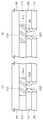
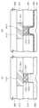
도 2은 본 발명의 다른 실시예에 따른 전기 소자를 설명하는 단면도이다.2 is a cross-sectional view illustrating an electrical device according to another embodiment of the present invention.
도 2를 참조하면, 기판(200)은 셀 영역(A) 과 퓨즈 영역(B)을 포함할 수 있다. 퓨즈 상변화 소자(10f)는 상기 퓨즈 영역(B)에 배치되고, 셀 상변화 소자(10c)는 상기 셀 영역(A)에 배치될 수 있다. 상기 퓨즈 상변화 소자(10f)는 상기 퓨즈 영역에 형성된 퓨즈 하부 배선(212f), 상기 퓨즈 하부 배선(212f) 상에 형성된 퓨즈 상변화 패턴(230f), 및 상기 퓨즈 상변화 패턴(230f) 상에 형성된 퓨즈 상부 배선(260f)을 포함할 수 있다. 상기 셀 상변화 소자(10c)는 상기 셀 영역(A)에 형성된 셀 하부 배선(212c), 상기 셀 하부 배선(212c) 상에 형성된 셀 상변화 패턴(230c), 및 상기 셀 상변화 패턴(230c) 상에 형성된 셀 상부 배선(260c)을 포함할 수 있다. 상기 퓨즈 상변화 패턴(230f)의 결정화 온도는 상기 셀 상변화 패턴(230c)의 결정화 온도보다 높을 수 있다. 셀 하부 전극(224c)은 상기 셀 상변화 패턴(230c)과 상기 셀 하부 배선(214c) 사이에 배치될 수 있다. 퓨즈 하부 전극(224f)은 상기 퓨즈 상변화 패턴(230f)과 상기 퓨즈 하부 배선(214f) 사이에 배치될 수 있다.Referring to FIG. 2, the
상기 기판(200)은 반도체 기판 또는 유전체 기판일 수 있다. 상기 기판(200) 은 실리콘(Si) 기판, 게루마늄(Ge) 기판, 및 SOI(silicon on insulator) 기판 중에서 적어도 하나를 포함할 수 있다. 상기 기판은 셀 영역(A) 과 퓨즈 영역(B)을 포함할 수 있다. 상기 기판(200)은 하부 구조물(미도시)을 포함할 수 있다. 상기 하부 구조물은 다이오드 또는 트랜지스터를 포함할 수 있다.The
하부 층간 절연막(210)이 상기 기판(200) 상에 배치될 수 있다. 상기 하부 층간 절연막(210)은 실리콘 산화막으로 형성될 수 있다. 상기 하부 층간 절연막(210)의 상부면은 평탄화될 수 있다. 상기 하부 층간 절연막(210)을 관통하는 하부 콘택홀(214c,214f) 내에 하부 배선(212c,212f)이 배치될 수 있다. 상기 하부 배선(212c,212f)은 도전성 패드를 포함할 수 있다. 상기 하부 배선(212c,212f)은 금속, 금속화합물, 도핑된 반도체 중에서 적어도 하나를 포함할 수 있다. 상기 하부 배선(212c,212f)은 상기 셀 영역(A)에 형성된 셀 하부 배선(212c), 및 상기 퓨즈 영역(B)에 형성된 퓨즈 하부 배선(212f)을 포함할 수 있다. 상기 하부 층간 절연막(210)의 상부면과 상기 하부 배선(212c,212f)의 상부면의 높이는 같을 수 있다.A lower
중간 층간 절연막(220)이 상기 하부 배선(212c,212f) 및/또는 상기 하부 층간 절연막(210) 상에 배치될 수 있다. 상기 중간 층간 절연막(220)은 실리콘 산화막일 수 있다. 상기 중간 층간 절연막(220)을 관통하여 상기 하부 배선(212c,212f)을 노출하는 중간 콘택홀(226c,226f)이 배치될 수 있다. 상기 중간 콘택 홀(226c,226f)은 상기 셀 영역(A)에 형성된 셀 중간 콘택홀(226c) 및 상기 퓨즈 영역(B)에 형성된 퓨즈 중간 콘택홀(226f)을 포함할 수 있다. 상기 중간 층간 절연막(220)은 실리콘산화막일 수 있다. 상기 중간 콘택홀(226c,226f)의 측벽에 하부 전극 스페이서(222c,222f)가 배치될 수 있다. 상기 하부 전극 스페이서(222c,222f)는 실리콘질화막 또는 실리콘산화질화막을 포함할 수 있다. 상기 하부 전극 스페이서(222c,222f)는 상기 셀 영역(A)에 형성된 셀 하부 전극 스페이서(222c) 및 상기 퓨즈 영역(B)에 형성된 퓨즈 하부 전극 스페이서(222f)를 포함할 수 있다. 하부 전극(224c,224f)은 상기 중간 콘택홀(226c,226f) 내에 배치될 수 있다. 상기 하부 전극(224c,224f)은 상기 상변화 패턴(230c,230f)을 가열하는 수단일 수 있다. 상기 하부 전극(224c,224f)은 상기 셀 영역(A)에 형성된 셀 하부 전극(224c) 및 상기 퓨즈 영역(B)에 형성된 퓨즈 하부 전극(224f)을 포함할 수 있다. 상기 하부전극(224c,224f)의 상부면과 상기 중간 층간 절연막(220)의 상부면은 같은 높이일 수 있다. 상기 하부 전극(224c,224f)은 금속 질화물, 금속, 금속 산화질화물, 실리사이드, 도전성 카본 중에서 적어도 하나를 포함할 수 있다. 구체적으로, 상기 하부 전극(224c,224f)은 Ti, Ta, Mo,W, TiN,TaN,WN,MoN, NbN, TiSiN, TiAlN, TiBN, ZrSiN, WSiN,WBN, ZrAlN, MoSiN, TaSiN, TaAlN, TiW,TiSi,TaSi, TiON, TiAlON, WON, TaON 중에서 적어도 하나를 포함할 수 있다. 상기 하부 전극 스페이스(222c,222f)의 열 전도도는 상기 중간 층간 절연막(220)의 열 전도도 보다 작을 수 있다.An intermediate
상부 층간 절연막(240)이 상기 중간 층간 절연막(220) 상에 배치될 수 있다. 상기 상부 층간 절연막(240)은 실리콘산화막일 수 있다. 상기 상부 층간 절연막(240)을 관통하여 상기 하부 전극(224c,224f)을 노출하는 상변화 콘택홀(236c,236f)이 배치될 수 있다. 상기 상변화 콘택 홀(236c,236f)은 상기 셀 영 역(A)에 형성된 셀 상변화 콘택홀(236c) 및 상기 퓨즈 영역(B)에 형성된 퓨즈 상변화 콘택홀(236f)을 포함할 수 있다. 상기 상변화 콘택홀(236c,236f)의 측벽에 상변화 스페이서(231c,231f)가 배치될 수 있다. 상기 상변화 스페이서(231c,231f)는 실리콘질화막 또는 실리콘산화질화막을 포함할 수 있다. 상기 상변화 스페이서(231c,231f)의 열 전도도는 상기 상부 층간 절연막(240)의 열 전도도 보다 작을 수 있다. 상기 상변화 스페이서(231c,231f)는 확산 방지막으로 작용할 수 있다. 상기 상변화 스페이서(231c,231f)는 상기 셀 영역(A)에 형성된 셀 상변화 스페이서(231c) 및 상기 퓨즈 영역에 형성된 퓨즈 상변화 스페이서(231f)를 포함할 수 있다. 상기 상변화 패턴(230c,230f)은 상기 상변화 콘택홀(236c,236f) 내에 배치될 수 있다. 상기 상변화 패턴(230c,230f)은 상기 셀 영역(A)에 형성된 셀 상변화 패턴(230c) 및 상기 퓨즈 영역(B)에 형성된 퓨즈 상변화 패턴(230f)을 포함할 수 있다.An upper
본 발명의 변형된 실시예에 따르면, 상기 상변화 패턴(230c,230f)은 콘택 플러그 형태에 한정되는 것은 아니다. 상기 상변화 패턴(230c,230f)은 상기 라인 형태를 가질 수 있다. 상기 상변화 패턴(230c,230f)은 상기 상부 배선(260c,260f)과 평행하게 연장될 수 있다.According to a modified embodiment of the present invention, the
상기 셀 상변화 패턴(230c)은 Ge-Sb-Te, Sb-Te, As-Sb-Te, Sb-Se 중에서 적어도 하나를 포함할 수 있다. 구체적으로, 상기 셀 상변화 패턴(230c)은 Ge2Sb2Te5일 수 있다. 상기 셀 상변화 패턴(230c)은 As-Sb-Te-금속 화합물, As-Ge-Sb-Te-금속 화합물, 금속-Sb-Te-금속 화합물, 5A족 원소-Sb-Te-금속 화합물, 6A족 원소- Sb-Te-금속 화합물, 5A족 원소-Sb-Se-금속 화합물, 6A족 원소-Sb-Se-금속 화합물 중에서 적어도 하나를 포함할 수 있다. 상기 화합물들의 조성비는 다양하게 변할 수 있다. 구체적으로 상기 5A원소는 N(질소),P(인)일 수 있고, 상기 6A원소는 O(산소), S(황)일 수 있다. 상기 셀 상변화 패턴(230c)은 역절두 원뿔형(inverse truncated cone)일 수 있다.The cell
상기 퓨즈 상변화 패턴(230f)은 제1 퓨즈 상변화 패턴(232f) 및 제2 퓨즈 상변화 패턴(234f)을 포함할 수 있다. 상기 제1 퓨즈 상변화 패턴(232f)의 결정화 온도는 상기 제2 퓨즈 상변화 패턴(234f)의 결정화 온도보다 높을 수 있다. 상기 제1 퓨즈 상변화 패턴(232f)의 결정화 온도는 섭씨 300도 이상일 수 있다. 상기 제1 퓨즈 상변화 패턴(232f)은 결정화 온도가 높은 물질을 사용하고, 상기 셀 상변화 패턴(230c)은 메모리 특성이 좋은 물질을 사용할 수 있다. 상기 제1 퓨즈 상변화 패턴(232f)은 항아리 모양일 수 있다. 상기 제1 퓨즈 상변화 패턴(232f)은 상기 퓨즈 상변화 스페이서(231f)의 측면과 접촉할 수 있다. 상기 제1 퓨즈 상변화 패턴(232f)의 하부면은 상기 퓨즈 하부 전극(224f)의 상부면과 접촉할 수 있다. 상기 제2 퓨즈 상변화 패턴(234f)은 상기 제1 퓨즈 상변화 패턴(232f)의 내부를 채울 수 있다. 상기 제2 퓨즈 상변화 패턴(234f)은 역절두 원뿔형일 수 있다. 상기 제1 퓨즈 상변화 패턴(232f) 및 상기 제2 퓨즈 상변화 패턴(234f)의 상부면은 동일한 높이를 가질 수 있다.The fuse
상기 제1 퓨즈 상변화 패턴(232f)은 In-Sb-Te, 5A족 원소-In-Sb-Te 화합물, 6A족 원소-In-Sb-Te 화합물 중에서 적어도 하나를 포함할 수 있다. 상기 제1 퓨즈 상변화 패턴(232f)의 결정화 온도는 상기 셀 상변화 패턴(230c)의 결정화 온도보다 높을 수 있다. 상기 제2 퓨즈 상변화 패턴(234f)과 상기 셀 상변화 패턴(230c)은 같은 물질일 수 있다. 상기 퓨즈 하부 전극(224f)에 흐르는 전류에 의하여 상기 제1 퓨즈 상변화 패턴(232f)이 상변화될 수 있다. 상기 제1 퓨즈 상변화 패턴(232f)의 저항 상태는 적외선 리플로우 공정에 의하여 변하지 않을 수 있다. 상기 퓨즈 상변화 소자는 일회성 플로그램 셀(one time program cell)로 사용될 수 있다.The first fuse
상기 상변화 패턴(230c,230f) 상에 상부 배선(260c,260f)이 배치될 수 있다. 상기 상부 배선(260c,260f)은 상기 셀 영역(A)에 형성된 셀 상부 배선(260c) 및 상기 퓨즈 영역(B)에 형성된 퓨즈 상부 배선(260f)을 포함할 수 있다. 상기 상부 배선(260c,260f)은 상기 상변화 패턴(230c,230f)과 전기적으로 연결될 수 있다. 상기 상부 배선(260c,260f)은 금속, 금속화합물, 도핑된 반도체 중에서 적어도 하나를 포함할 수 있다. 상기 상부 배선(260c,260f)은 상기 셀 영역에 형성된 셀 상부 배선(260c) 및 상기 퓨즈 영역(B)에 형성된 퓨즈 상부 배선(260f)을 포함할 수 있다. 상기 셀 상부 배선(260c)은 확산방지층(262c)/금속층(264c)/확산방지층(266c)의 복층 구조를 가질 수 있다. 상기 퓨즈 상부 배선(260f)은 확산방지층(262f)/금속층(264f)/확산방지층(266f)의 복층 구조를 가질 수 있다.
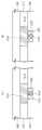
도 3은 본 발명의 또 다른 실시예에 따른 전기 소자를 설명하는 단면도이다.3 is a cross-sectional view illustrating an electrical device according to still another embodiment of the present invention.
도 3를 참조하면, 상기 전기 소자는 도 2에서 설명한 전기 소자와 유사한 구조를 가진다. 따라서, 중복되는 설명은 생략한다. 기판(300)은 셀 영역(A) 과 퓨즈 영역(B)을 포함할 수 있다. 퓨즈 상변화 소자(10f)는 상기 퓨즈 영역(B)에 배치되 고, 셀 상변화 소자(10c)는 상기 셀 영역(A)에 배치될 수 있다. 상기 퓨즈 상변화 소자(10f)는 상기 퓨즈 영역(B)에 형성된 퓨즈 하부 배선(312f), 상기 퓨즈 하부 배선(312f) 상에 형성된 퓨즈 상변화 패턴(330f), 및 상기 퓨즈 상변화 패턴(330f) 상에 형성된 퓨즈 상부 배선(360f)을 포함할 수 있다. 상기 셀 상변화 소자(10c)는 상기 셀 영역(A)에 형성된 셀 하부 배선(312c), 상기 셀 하부 배선(312c) 상에 형성된 셀 상변화 패턴(330c), 및 상기 셀 상변화 패턴(330c) 상에 형성된 셀 상부 배선(360c)을 포함할 수 있다. 상기 퓨즈 상변화 패턴(330f)의 결정화 온도는 상기 셀 상변화 패턴(330c)의 결정화 온도보다 높을 수 있다.Referring to FIG. 3, the electric element has a structure similar to that of the electric element described with reference to FIG. 2. Therefore, redundant description is omitted. The
상기 하부 층간 절연막(310)은 기판(300) 상에 배치될 수 있다. 상기 하부 배선(312c,312f)은 상기 하부 층간 절연막(310)의 내부에 배치될 수 있다. 상기 하부 층간 절연막(310) 상에 중간 층간 절연막(320)이 배치될 수 있다. 상기 중간 층간 절연막 내에 하부 전극(324c,324f)이 배치될 수 있다. 하부 전극(324c,324f)은 상기 하부 배선(312c,312f)과 전기적으로 연결될 수 있다. 상기 하부 전극(324c,324f)은 상기 셀 영역(A)에 배치된 셀 하부 전극(324c) 및 상기 퓨즈 영역(B)에 배치된 퓨즈 하부 전극(324f)을 포함할 수 있다. 하부 전극 스페이서(322c,322f)는 상기 하부 전극과 상기 중간 층간 절연막 사이에 배치될 수 있다. 상기 하부 전극 스페이서(322c,322f)는 상기 셀 영역(A)에 배치된 셀 하부 전극 스페이서(322c)와 상기 퓨즈 영역(B)에 배치된 퓨즈 하부 전극 스페이서(322f)를 포함할 수 있다.The lower
상기 중간 층간 절연막 상에 상부 층간 절연막(340)이 배치될 수 있다. 상기 상부 층간 절연막(340) 내에 상변화 패턴(330c,330f)이 배치될 수 있다. 상기 상변화 패턴(330c,330f)은 상기 셀 영역(A)에 배치된 셀 상변화 패턴 (330c) 및 상기 퓨즈 영역(B)에 배치된 퓨즈 상변화 패턴(330f)을 포함할 수 있다.An upper
상기 셀 상변화 패턴(330c)은 항아리 모양일 수 있다. 상기 셀 상변화 패턴(330c)의 내부는 셀 상부 전극(336c)으로 채워질 수 있다. 상기 셀 상변화 패턴(330c) 및 상기 셀 상부 전극(336c)의 상부면은 같은 높이일 수 있다.The cell
상기 퓨즈 상변화 패턴(330f)은 제1 퓨즈 상변화 패턴(332f) 및 상기 제2 퓨즈 상변화 패턴(334f)을 포함할 수 있다. 항아리 모양의 상기 제2 퓨즈 상변화 패턴(334f)은 항아리 모양의 상기 제1 퓨즈 상변화 패턴(332f) 내에 배치될 수 있다. 상기 퓨즈 상부 전극(336f)은 항아리 모양의 상기 제2 퓨즈 상변화 패턴(334f)의 내부에 배치될 수 있다. 상기 퓨즈 상변화 패턴(330f) 및 상기 퓨즈 상부 전극(336f)의 상부면은 같은 높이일 수 있다. 상기 제1 퓨즈 상변화 패턴(332f)의 결정화 온도는 상기 제2 퓨즈 상변화 패턴(334f)의 결정화 온도보다 높을 수 있다. 또한, 상기 제2 퓨즈 상변화 패턴(334f)은 상기 셀 상변화 패턴(330c)과 같은 물질일 수 있다.The fuse
본 발명의 변형된 실시예에 따르면, 상기 상변화 패턴(330c,330f)은 상기 상부 배선(360c,360f) 방향으로 연장될 수 있다. 상기 상변화 패턴의 형태는 다양하게 변형될 수 있다.According to a modified embodiment of the present invention, the
상기 상부 배선(360c,360f)은 상기 상부 전극(336c,336f) 및 상기 상변화 패턴(330c,330f) 상에 배치될 수 있다. 상기 상부 배선(360c,360f)은 상기 셀 영 역(A)에 배치된 셀 상부 배선(360c) 및 상기 퓨즈 영역(B)에 배치된 퓨즈 상부 배선(360f)을 포함할 수 있다. 상기 셀 상부 배선(360c)은 확산방지층(362c)/금속층(364c)/확산방지층(366c)의 복층 구조를 가질 수 있다. 상기 퓨즈 상부 배선(360f)은 확산방지층(362f)/금속층(364f)/확산방지층(366f)의 복층 구조를 가질 수 있다.The
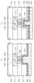
도 4은 본 발명의 또 다른 실시예에 따른 전기 소자를 설명하는 단면도이다.4 is a cross-sectional view illustrating an electrical device according to still another embodiment of the present invention.
도 4를 참조하면, 상기 전기 소자는 도 3에서 설명한 전기 소자와 유사한 구조를 가진다. 기판(400)은 셀 영역(A) 과 퓨즈 영역(B)을 포함할 수 있다. 퓨즈 상변화 소자(10f)는 상기 퓨즈 영역(B)에 배치되고, 셀 상변화 소자(10c)는 상기 셀 영역(A)에 배치될 수 있다. 상기 퓨즈 상변화 소자(10f)는 상기 퓨즈 영역(B)에 형성된 퓨즈 하부 배선(412f), 상기 퓨즈 하부 배선(412f) 상에 형성된 퓨즈 상변화 패턴(432f), 및 상기 퓨즈 상변화 패턴(432f) 상에 형성된 퓨즈 상부 배선(460f)을 포함할 수 있다. 상기 셀 상변화 소자(10c)는 상기 셀 영역(A)에 형성된 셀 하부 배선(412c), 상기 셀 하부 배선(412c) 상에 형성된 셀 상변화 패턴(434c), 및 상기 셀 상변화 패턴(434c) 상에 형성된 셀 상부 배선(460c)을 포함할 수 있다. 상기 퓨즈 상변화 패턴(432f)의 결정화 온도는 상기 셀 상변화 패턴(434c)의 결정화 온도보다 높을 수 있다.Referring to FIG. 4, the electric element has a structure similar to that of the electric element described with reference to FIG. 3. The
상기 하부 층간 절연막(410)은 기판(400) 상에 배치될 수 있다. 상기 하부 배선(412c,412f)은 상기 하부 층간 절연막(410)의 내부에 배치될 수 있다. 상기 하부 층간 절연막(410) 상에 중간 층간 절연막(420)이 배치될 수 있다.The lower
상기 중간 층간 절연막(430) 내에 상기 상변화 패턴(430c,430f)이 배치될 수 있다. 상기 셀 상변화 패턴(430c)의 측면에는 셀 상변화 스페이서(432c)가 배치될 수 있고, 상기 퓨즈 상변화 패턴(430f)의 측면에는 퓨즈 상변화 스페이서(432f)가 배치될 수 있다. 상기 상변화 패턴(430c,430f)은 별도의 가열 소자에 의하여 열을 전달받아 상변화하지 않을 수 있다. 상기 상변화 패턴((430c,430f))에 흐르는 전류에 의하여 상변화할 수 있다. 상기 셀 상변화 패턴(430c)은 Ge-Sb-Te, Sb-Te, As-Sb-Te, Sb-Se 중에서 적어도 하나를 포함할 수 있다. 상기 퓨즈 상변화 패턴(430f)은 In-Sb-Te, 5A족 원소-In-Sb-Te 화합물, 6A족 원소-In-Sb-Te 화합물 중에서 적어도 하나를 포함할 수 있다.The
상기 상부 배선(460c,460f)은 상기 셀 영역(A)에 배치된 셀 상부 배선(460c) 및 상기 퓨즈 영역(B)에 배치된 퓨즈 상부 배선(460f)을 포함할 수 있다. 상기 셀 상부 배선(460c)은 확산방지층(462c)/금속층(464c)/확산방지층(466c)의 복층 구조를 가질 수 있다. 상기 퓨즈 상부 배선(460f)은 확산방지층(462f)/금속층(464f)/확산방지층(466f)의 복층 구조를 가질 수 있다. The
도 5는 본 발명의 또 다른 실시예에 따른 전기 소자를 설명하는 단면도들이다.5 is a cross-sectional view illustrating an electrical device according to still another embodiment of the present invention.
도 5를 참조하면, 상기 전기 소자는 도 2에서 설명한 전기 소자와 유사한 구조를 가진다. 기판(500)은 셀 영역(A) 과 퓨즈 영역(B)을 포함할 수 있다. 퓨즈 상변화 소자(10f)는 상기 퓨즈 영역(B)에 배치되고, 셀 상변화 소자(10c)는 상기 셀 영역(A)에 배치될 수 있다. 상기 퓨즈 상변화 소자(10f)는 상기 퓨즈 영역(B)에 형성된 퓨즈 하부 배선(512f), 상기 퓨즈 하부 배선(512f) 상에 형성된 퓨즈 하부 전극(524f), 상기 퓨즈 하부 전극(524f) 상에 형성된 퓨즈 상변화 패턴(530f), 및 상기 퓨즈 상변화 패턴(530f) 상에 형성된 퓨즈 상부 배선(560f)을 포함할 수 있다. 상기 셀 상변화 소자(10c)는 상기 셀 영역(A)에 형성된 셀 하부 배선(512c), 상기 셀 하부 배선(512c) 상에 형성된 셀 하부 전극(524c), 상기 셀 하부 전극(524c) 상에 형성된 셀 상변화 패턴(530c), 및 상기 셀 상변화 패턴(530c) 상에 형성된 셀 상부 배선(560c)을 포함할 수 있다. 상기 퓨즈 상변화 패턴(530f)의 결정화 온도는 상기 셀 상변화 패턴(530c)의 결정화 온도보다 높을 수 있다.Referring to FIG. 5, the electric element has a structure similar to that of the electric element described with reference to FIG. 2. The
상기 하부 층간 절연막(510)은 기판(500) 상에 배치될 수 있다. 하부 배선(512c,512f)은 상기 하부 층간 절연막(510)의 내부에 배치될 수 있다. 상기 하부 배선(512c,512f)은 상기 셀 영역(A)에 형성된 상기 셀 하부 배선(512c) 및 상기 퓨즈 영역(B)에 형성된 상기 퓨즈 하부 배선(512f)을 포함할 수 있다.The lower
상기 하부 층간 절연막(510) 상에 상부 층간 절연막(540)이 배치될 수 있다.An upper
상기 상부 층간 절연막(540) 내에 하부 전극(524c,524f) 및 상기 상변화 패턴(530c,530f)이 차례로 적층될 수 있다. 상기 하부 전극(524c,524f)은 상기 셀 영역(A)에 형성된 셀 하부 전극(524c) 및 상기 퓨즈 영역(B)에 형성된 퓨즈 하부 전극(524f)을 포함할 수 있다. 상기 상변화 패턴(530c,530f)은 상기 셀 영역(A)에 형성된 셀 상변화 패턴(530c) 및 상기 퓨즈 영역(B)에 형성된 퓨즈 상변화 패턴(530f)을 포함할 수 있다.
상기 셀 상변화 패턴(530c) 및 상기 셀 하부 전극(524c)의 측면에는 셀 상변 화 스페이서(531c)가 배치될 수 있다. 상기 퓨즈 상변화 패턴(530f) 및 상기 퓨즈 하부 전극(524c)의 측면에는 퓨즈 상변화 스페이서(531f)가 배치될 수 있다. 상기 상변화 패턴(530c,530f)은 상기 하부 전극(524c,525f)에 의하여 열을 전달받아 상변화할 수 있다.A cell
상기 상부 배선(560c,560f)은 상기 셀 영역(A)에 배치된 셀 상부 배선(560c) 및 상기 퓨즈 영역(B)에 배치된 퓨즈 상부 배선(560f)을 포함할 수 있다. 상기 셀 상부 배선(560c)은 확산방지층(562c)/금속층(564c)/확산방지층(566c)의 복층 구조를 가질 수 있다. 상기 퓨즈 상부 배선(560f)은 확산방지층(562f)/금속층(564f)/확산방지층(566f)의 복층 구조를 가질 수 있다. The
도 6a 내지 도 6d는 본 발명의 일 실시예에 따른 전기 소자의 형성 방법을 설명하는 도면들이다.6A to 6D are diagrams illustrating a method of forming an electrical device according to an embodiment of the present invention.
도 6a를 참조하면, 기판(100)은 퓨즈 영역(B)과 셀 영역(A)을 포함할 수 있다. 상기 기판(100) 상에 하부 층간 절연막(110)이 형성된다. 상기 하부 층간 절연막(110)은 화학 기상 증착법 또는 스핀 코팅법에 의하여 형성될 수 있다. 상기 하부 층간 절연막(110)은 실리콘 산화막일 수 있다. 상기 하부 층간 절연막(110)의 상부면은 평탄화될 수 있다. 상기 하부 층간 절연막(110)을 패터닝하여 하부 콘택홀(114c,114f)을 형성할 수 있다. 상기 하부 콘택홀(114c,114f)은 상기 셀 영역(A)에 형성되는 셀 하부 콘택홀(114c) 및 상기 퓨즈 영역(B)에 형성되는 퓨즈 하부 콘택홀(114f)을 포함할 수 있다. 상기 셀 하부 콘택홀(114c)과 상기 퓨즈 하부 콘택홀(114f)은 동시에 형성될 수 있다. 하부 배선막(미도시)이 상기 하부 콘택홀(114c,114f) 및 상기 하부 층간 절연막(110)을 덮을 수 있다. 상기 하부 배선막이 증착된 상기 기판(100)을 평탄화하여 하부 배선(112c,112f)을 형성할 수 있다. 상기 하부 배선(112c,112f)은 상기 셀 영역(A)에 형성된 셀 하부 배선(112c) 및 상기 퓨즈 영역(B)에 형성된 퓨즈 하부 배선(112f)을 포함할 수 있다. 상기 평탄화는 화학 기계적 연마(chemical mechanical polishing) 공정 또는 에치백(etch back) 공정을 이용할 수 있다.Referring to FIG. 6A, the
도 6b를 참조하면, 상기 하부 배선(114f,114c) 및 하부 층간 절연막(110) 상에 제1 중간 층간 절연막(120) 및 제2 중간 층간 절연막(122)이 차례로 적층될 수 있다. 상기 제1 중간 층간 절연막(120)은 실리콘 산화막일 수 있다. 상기 제2 중간 층간 절연막(122)은 실리콘 질화막, 실리콘 산화질화막일 수 있다. 상기 제2 중간 층간 절연막(122) 및 제1 중간 층간 절연막(120)을 패터닝하여 상기 하부 배선(122c,112f)을 노출하는 중간 콘택홀(126c,126f)을 형성할 수 있다. 상기 중간 콘택홀(126c,126f)은 상기 셀 영역(A)에 형성된 셀 중간 콘택홀(126c) 및 상기 퓨즈 영역(B)에 형성된 퓨즈 중간 콘택홀(126f)을 포함할 수 있다.Referring to FIG. 6B, a first intermediate
도 6c를 참조하면, 하부 전극 스페이서막(미도시)이 상기 중간 콘택홀(126c,126f) 및 상기 제2 중간 층간 절연막(122) 상에 콘퍼멀하게 형성될 수 있다. 상기 하부 전극 스페이서막은 실리콘 질화막일 수 있다. 상기 하부 전극 스페이서막을 이방성 식각하여 상기 중간 콘택홀(126c,126f)의 측벽에 하부 전극 스페이서(122c,122f)를 형성할 수 있다. 상기 하부 전극 스페이서(122c,122f)는 상기 셀 영역(A)에 형성되는 셀 하부 전극 스페이서(122c)와 상기 퓨즈 영역(B)에 형성 되는 퓨즈 하부 전극 스페이서(122f)를 포함할 수 있다.Referring to FIG. 6C, a lower electrode spacer layer (not shown) may be formed on the intermediate contact holes 126c and 126f and the second intermediate
도 6d를 참조하면, 하부 전극막(미도시)이 상기 중간 콘택홀(126c,126f)을 채우도록 증착된다. 이어서, 상기 기판(100)은 상기 제1 중간 층간 절연막(120)이 노출될 때까지 평탄화될 수 있다. 이에 따라, 하부 전극(124c,124f)이 형성될 수 있다. 상기 하부 전극(124c,124f)은 상기 셀 영역(A)에 형성되는 셀 하부 전극(124c) 및 상기 퓨즈 영역(B)에 형성되는 퓨즈 하부 전극(124f)을 포함할 수 있다. 상기 하부 전극 스페이서(122c,122f)와 상기 하부 전극(124c,124f)의 상부면은 같은 높이를 가질 수 있다.Referring to FIG. 6D, a lower electrode film (not shown) is deposited to fill the intermediate contact holes 126c and 126f. Subsequently, the
다시 도 1을 참조하면, 상기 기판(100) 상에 제1 상변화막(미도시)을 증착한다. 이어서, 상기 셀 영역(A)의 제1 상변화막을 패터닝하여 제거한다. 이어서, 제2 상변화막(미도시), 상부 전극막(미도시), 및 하드 마스크막(미도시)을 차례로 적층할 수 있다. 상기 셀 영역(A)에서 상기 하드 마스크막, 상부 전극막, 제2 상변화막을 연속적으로 패터닝하여 셀 하드 마스크 패턴(138c), 셀 상부 전극(136c), 셀 상변화 패턴(130c)을 형성할 수 있다. 상기 퓨즈 영역(B)에서 상기 하드 마스크막, 상부 전극막, 제2 상변화막, 및 제1 상변화막을 연속적으로 패터닝하여 퓨즈 하드 마스크 패턴(138f), 퓨즈 상부 전극(136f), 퓨즈 상변화 패턴(130f)을 형성할 수 있다. 상기 퓨즈 상변화 패턴(130f)은 제1 퓨즈 상변화 패턴(132f) 및 제2 퓨즈 상변화 패턴(134f)을 포함할 수 있다.Referring back to FIG. 1, a first phase change film (not shown) is deposited on the
상기 하드 마스크 패턴(138c,138f) 및 상기 제1 중간 층간 절연막(120) 상에 보호막(142)을 콘퍼멀하게 형성할 수 있다. 상기 보호막(142)은 실리콘 질화막일 수 있다. 상기 보호막(142)이 형성된 상기 기판(100) 상에 상부 층간 절연막(140)을 형성할 수 있다. 상기 상부 층간 절연막(140)의 상부면은 평탄화될 수 있다. 상기 상부 층간 절연막(140)의 상부면은 상기 하드 마스크 패턴(138c,138c)의 상부면 보다 높을 수 있다. 상기 상부 층간 절연막(140)을 상기 상부 전극(136c,136f)이 노출되도록 패터닝하여 상부 콘택홀(156c,156f)을 형성할 수 있다. 상기 상부 콘택홀(156c,156f)은 상기 셀 영역(A)에 형성되는 셀 상부 콘택홀(156c) 및 상기 퓨즈 영역(B)에 형성되는 퓨즈 상부 콘택홀(156f)을 포함할 수 있다. 도전막(미도시)은 상기 상부 콘택홀(156c,156f) 및 상기 상부 층간 절연막(140) 상에 형성될 수 있다. 상기 도전막은 상기 상부 콘택홀(156c,156f)을 채울 수 있다. 이어서, 상기 도전막이 증착된 상기 기판(100)을 평탄화하여 상부 콘택 플러그(150c,150f)를 형성할 수 있다. 상기 상부 콘택 플러그(150c,150f)는 상기 셀 영역(A)에 형성된 셀 상부 콘택 플러그(150c)와 상기 퓨즈 영역(B)에 형성된 퓨즈 상부 콘택 플러그(150f)를 포함할 수 있다. 상기 셀 상부 콘택 플러그(150c)는 확산방지층(154c)과 도전층(152c)의 복층 구조를 포함할 수 있다. 상기 퓨즈 상부 콘택 플러그(150f)는 확산방지층(154f)과 도전층(152f)의 복층 구조를 포함할 수 있다.The
상기 상부 콘택 플러그(150c,150f)가 형성된 상기 기판(100) 상에 상부 배선막(미도시)이 형성될 수 있다. 상기 상부 배선막을 패터닝하여 상부 배선(160c,160f)을 형성할 수 있다. 상기 상부 배선(160c,160f)은 상기 셀 영역(A)에 형성되는 셀 상부 배선(160c) 및 상기 퓨즈 영역(B)에 형성되는 퓨즈 상부 배선(160f)을 포함할 수 있다. 상기 셀 상부 배선(160c) 및 상기 퓨즈 상부 배 선(160f)은 확산방지층(162)/배선층(164)/확산방지층(166)의 복층구조를 포함할 수 있다.An upper wiring layer (not shown) may be formed on the
도 7a 내지 도 7f는 본 발명의 다른 실시예에 따른 전기 소자의 형성 방법을 설명하는 단면도들이다. 7A to 7F are cross-sectional views illustrating a method of forming an electrical device according to another embodiment of the present invention.
도 7a를 참조하면, 기판(200)은 퓨즈 영역(B)과 셀 영역(A)을 포함할 수 있다. 상기 기판(200) 상에 하부 층간 절연막(210)이 형성될 수 있다. 상기 하부 층간 절연막(210)은 화학 기상 증착법 또는 스핀 코팅법에 의하여 형성될 수 있다. 상기 하부 층간 절연막(210)은 실리콘 산화막일 수 있다. 상기 하부 층간 절연막(210)의 상부면은 평탄화될 수 있다. 상기 하부 층간 절연막(210)을 패터닝하여 하부 콘택홀(214c,214f)을 형성할 수 있다. 상기 하부 콘택홀(214c)은 상기 셀 영역(A)에 형성되는 셀 하부 콘택홀(214c) 및 상기 퓨즈 영역(B)에 형성되는 퓨즈 콘택홀(214f)을 포함할 수 있다. 상기 셀 하부 콘택홀(214c)과 상기 퓨즈 하부 콘택홀(214f)은 동시에 형성될 수 있다. 하부 배선막(미도시)이 상기 하부 콘택홀(214c,214f) 및 상기 하부 층간 절연막(210)을 덮을 수 있다. 상기 하부 배선막이 증착된 상기 기판(200)을 평탄화하여 하부 배선(212c,212f)을 형성할 수 있다. 상기 하부 배선(212c,212f)은 상기 셀 영역(A)에 형성된 셀 하부 배선(212c) 및 상기 퓨즈 영역(B)에 형성된 퓨즈 하부 배선(212f)을 포함할 수 있다. 상기 평탄화는 화학 기계적 연마(chemical mechanical polishing) 공정 또는 에치백(etch back) 공정을 이용할 수 있다.Referring to FIG. 7A, the
도 7b를 참조하면, 상기 하부 배선(214f,214c) 및 하부 층간 절연막(210) 상 에 제1 중간 층간 절연막(220) 및 제2 중간 층간 절연막(222)이 차례로 적층될 수 있다. 상기 제1 중간 층간 절연막(220)은 실리콘 산화막일 수 있다. 상기 제2 중간 층간 절연막(222)은 실리콘 질화막, 실리콘 산화질화막일 수 있다. 상기 제2 중간 층간 절연막(222) 및 제1 중간 층간 절연막(220)을 패터닝하여 상기 하부 배선(212c,212f)을 노출하는 중간 콘택홀(226c,226f)을 형성할 수 있다. 상기 중간 콘택홀(226c,226f)은 상기 셀 영역(A)에 형성된 셀 중간 콘택홀(226c) 및 상기 퓨즈 영역(B)에 형성된 퓨즈 중간 콘택홀(226f)을 포함할 수 있다.Referring to FIG. 7B, a first intermediate
하부 전극 스페이서막(미도시)이 상기 중간 콘택홀(226c,226f) 및 상기 제2 중간 층간 절연막(222) 상에 콘퍼멀하게 형성될 수 있다. 상기 하부 전극 스페이서막은 실리콘 질화막일 수 있다. 상기 하부 전극 스페이서막을 이방성 식각하여 상기 중간 콘택홀(226c,226f)의 측벽에 하부 전극 스페이서(222c,222f)를 형성할 수 있다. 상기 하부 전극 스페이서(222c,222f)는 상기 셀 영역(A)에 형성되는 셀 하부 전극 스페이서(222c)와 상기 퓨즈 영역(B)에 형성되는 퓨즈 하부 전극 스페이서(222f)를 포함할 수 있다.A lower electrode spacer layer (not shown) may be formed conformally on the intermediate contact holes 226c and 226f and the second intermediate
하부 전극막(미도시)이 상기 중간 콘택홀(226c,226f)을 채우도록 증착된다. 이어서, 상기 기판(200)은 상기 제1 중간 층간 절연막(220)이 노출될 때까지 평탄화될 수 있다. 이에 따라, 하부 전극(224c,224f)이 형성될 수 있다. 상기 하부 전극(224c,224f)은 상기 셀 영역(A)에 형성되는 셀 하부 전극(224c) 및 상기 퓨즈 영역(B)에 형성되는 퓨즈 하부 전극(224f)을 포함할 수 있다.A lower electrode film (not shown) is deposited to fill the intermediate contact holes 226c and 226f. Subsequently, the
도 7d를 참조하면, 상기 하부 전극(224c,224f) 상에 상부 층간절연막(240)이 형성될 수 있다. 상기 상부 층간 절연막(240)은 실리콘 산화막일 수 있다. 상기 상부 층간 절연막(240)을 상기 하부 전극(224c,224f)이 노출되도록 패터닝하여 상변화 콘택홀(236c,236f)을 형성할 수 있다. 상기 상변화 콘택홀(236c,236f)은 상기 셀 영역(A)에 형성된 셀 상변화 콘택홀(236c) 및 상기 퓨즈 영역(B)에 형성된 퓨즈 상변화 콘택홀(236f)을 포함할 수 있다.Referring to FIG. 7D, an upper
상변화 스페이서막(미도시)이 상기 상변화 콘택홀(236c,236f) 및 상기 상부 층간 절연막(240) 상에 콘퍼멀하게 형성될 수 있다. 상기 상변화 스페이서막을 이방성 식각하여 상기 상변화 콘택홀(236c,236f)의 측벽에 상변화 스페이서(231c,231f)를 형성할 수 있다. 상기 상변화 스페이서(231c,231f)는 상기 셀 영역(A)에 형성되는 셀 상변화 스페이서(231c)와 상기 퓨즈 영역(B)에 형성되는 퓨즈 상변화 스페이서(231f)를 포함할 수 있다. 상기 상변화 스페이서(231c,231f)는 실리콘 질화막일 수 있다. 상기 상변화 스페이서가 형성된 상기 기판(200) 상에 제1 상변화막(232)을 콘퍼멀하게 증착할 수 있다.A phase change spacer layer (not shown) may be formed on the phase change contact holes 236c and 236f and the upper
본 발명의 변형된 실시예에 따르면, 상기 상변화 콘택홀(236c,236f)은 트렌치 형태일 수 있다. 상기 상변화 스페이서(231c,231f)는 상기 트렌치의 측벽에 배치될 수 있다.According to a modified embodiment of the present invention, the phase change contact holes 236c and 236f may be in the form of trenches. The
도 7e를 참조하면, 상기 셀 영역(A)의 상기 제1 상변화막(232)을 제거할 수 있다. 상기 제1 상변화막(232)의 제거는 이방성 식각에 의하여 수행될 수 있다. 이어서, 상기 기판(200) 상에 제2 상변화막(234)을 증착할 수 있다. 상기 제2 상변화막(234)은 상기 상변화 콘택홀(236c,236f)을 채울 수 있다.Referring to FIG. 7E, the first
도 7f를 참조하면, 상기 제2 상변화막(234)이 증착된 상기 기판(200)을 상기 상부 층간 절연막(240)이 노출되도록 평탄화하여 상변화 패턴(230c,230f)을 형성할 수 있다. 상기 상변화 패턴(230c,230f)은 상기 셀 영역(A)에 형성된 셀 상변화 패턴(230c) 및 상기 퓨즈 영역(B)에 형성된 퓨즈 상변화 패턴(230f)을 포함할 수 있다. 상기 퓨즈 상변화 패턴(230f)은 제1 퓨즈 상변화 패턴(232f) 및 상기 제2 퓨즈 상변화 패턴(234f)을 포함할 수 있다.Referring to FIG. 7F,
본 발명의 변형된 실시예에 따르면, 상변화 패턴(230c,230f)은 트레치 형태의 상기 상변화 콘택홀236c,236f)을 채우는 라인 형태일 수 있다.According to a modified embodiment of the present invention, the
다시 도 2를 참조하면, 상기 상변화 패턴(230c,230f) 상에 상부 배선막(미도시)을 형성할 수 있다. 상기 상부 배선막을 패터닝하여 상부 배선(260c,260f)을 형성할 수 있다. 상기 상부 배선(260c,260f)은 상기 셀 영역(A)에 형성되는 셀 상부 배선(260c) 및 상기 퓨즈 영역(B)에 형성되는 퓨즈 상부 배선(260f)을 포함할 수 있다. 상기 셀 상부 배선(260c)은 확산방지층(262c)/배선층(264c)/확산방지층(266c)의 복층구조를 포함할 수 있다. 상기 퓨즈 상부 배선(260f)은 확산방지층(262f)/배선층(264f)/확산방지층(266f)의 복층구조를 포함할 수 있다.Referring to FIG. 2 again, an upper wiring layer (not shown) may be formed on the
도 8a 내지 도 8e는 본 발명의 또 다른 실시예에 따른 전기 소자의 형성 방법을 설명하는 단면도들이다.8A to 8E are cross-sectional views illustrating a method of forming an electrical device according to still another embodiment of the present invention.
도 8a를 참조하면, 기판(300)은 퓨즈 영역(B)과 셀 영역(A)을 포함할 수 있다. 상기 기판(300) 상에 하부 층간 절연막(310)이 형성될 수 있다. 상기 하부 층간 절연막(310)은 화학 기상 증착법 또는 스핀 코팅법에 의하여 형성될 수 있다. 상기 하부 층간 절연막(310)은 실리콘 산화막일 수 있다. 상기 하부 층간 절연막(310)의 상부면은 평탄화될 수 있다. 상기 하부 층간 절연막(310)을 패터닝하여 하부 콘택홀(314c,314f)을 형성할 수 있다. 상기 하부 콘택홀(314c,314f)은 상기 셀 영역(A)에 형성되는 셀 하부 콘택홀(314c) 및 상기 퓨즈 영역(B)에 형성되는 퓨즈 하부 콘택홀(314f)을 포함할 수 있다. 상기 셀 하부 콘택홀(314c)과 상기 퓨즈 하부 콘택홀(314f)은 동시에 형성될 수 있다. 하부 배선막(미도시)이 상기 하부 콘택홀(314c,314f) 및 상기 하부 층간 절연막(310) 상에 형성될 수 있다. 상기 하부 배선막이 증착된 상기 기판(300)을 평탄화하여 하부 배선(312c,312f)을 형성할 수 있다. 상기 하부 배선(312c,312f)은 상기 셀 영역(A)에 형성된 셀 하부 배선(312c) 및 상기 퓨즈 영역(B)에 형성된 퓨즈 하부 배선(312f)을 포함할 수 있다. 상기 평탄화는 화학 기계적 연마(chemical mechanical polishing) 공정 또는 에치백(etch back) 공정을 이용할 수 있다.Referring to FIG. 8A, the
도 8b를 참조하면, 상기 하부 배선(314f,314c) 및 하부 층간 절연막(310) 상에 제1 중간 층간 절연막(320) 및 제2 중간 층간 절연막(322)이 차례로 적층될 수 있다. 상기 제1 중간 층간 절연막(320)은 실리콘 산화막일 수 있다. 상기 제2 중간 층간 절연막(322)은 실리콘 질화막, 실리콘 산화질화막일 수 있다. 상기 제2 중간 층간 절연막(322) 및 제1 중간 층간 절연막(320)을 패터닝하여 상기 하부 배선(312c,312f)을 노출하는 중간 콘택홀(326c,326f)을 형성할 수 있다. 상기 중간 콘택홀(326c,326f)은 상기 셀 영역(A)에 형성된 셀 중간 콘택홀(326c) 및 상기 퓨즈 영역(B)에 형성된 퓨즈 중간 콘택홀(326f)을 포함할 수 있다.Referring to FIG. 8B, a first intermediate
도 8c를 참조하면, 하부 전극 스페이서막(미도시)이 상기 중간 콘택 홀(326c,326f) 및 상기 제2 중간 층간 절연막(322) 상에 콘퍼멀하게 형성될 수 있다. 상기 하부 전극 스페이서막은 실리콘 질화막일 수 있다. 상기 하부 전극 스페이서막을 이방성 식각하여 상기 중간 콘택홀(326c,326f)의 측벽에 하부 전극 스페이서(322c,322f)를 형성할 수 있다. 상기 하부 전극 스페이서(322c,322f)는 상기 셀 영역(A)에 형성되는 셀 하부 전극 스페이서(322c)와 상기 퓨즈 영역(B)에 형성되는 퓨즈 하부 전극 스페이서(322f)를 포함할 수 있다.Referring to FIG. 8C, a lower electrode spacer layer (not shown) may be formed on the intermediate contact holes 326c and 326f and the second intermediate
도 8d를 참조하면, 하부 전극막(미도시)이 상기 중간 콘택홀(326c,326f)을 채우도록 증착된다. 이어서, 상기 기판(300)을 상기 제1 중간 층간 절연막(320)이 노출되도록 평탄화하여 하부 전극(324c,324f)을 형성할 수 있다. 상기 하부 전극(324c,324f)은 상기 셀 영역(A)에 형성되는 셀 하부 전극(324c) 및 상기 퓨즈 영역(B)에 형성되는 퓨즈 하부 전극(324f)을 포함할 수 있다.Referring to FIG. 8D, a lower electrode film (not shown) is deposited to fill the intermediate contact holes 326c and 326f. Subsequently, the
도 8e를 참조하면, 상기 하부 전극(324c,324f) 상에 상부 층간 절연막(340)이 형성될 수 있다. 상기 상부 층간 절연막(340)은 실리콘 산화막일 수 있다. 상기 상부 층간 절연막(340)을 상기 하부 전극(324c,324f)이 노출되도록 패터닝하여 상변화 콘택홀(331c,331f)을 형성할 수 있다. 상기 제1 상변화막(332)은 상기 상변화 콘택홀(331c,331f) 및 상기 상부 층간 절연막(340) 상에 콘퍼멀하게 형성될 수 있다. 상기 셀 영역(A)의 상기 제1 상변화막(332)은 이방성 식각에 의하여 제거될 수 있다. 이어서, 제2 상변화막(334)이 상기 상변화 콘택홀(331c,331f) 및 상기 상부 층간 절연막(340) 상에 콘퍼멀하게 형성된다. 상기 제2 상변화막(334)은 상기 상변화 콘택홀(331c,331f)을 완전히 채우지 않을 수 있다. 상기 제2 상변화막(334) 상 에 상부 전극막(336)이 형성될 수 있다. 본 발명의 변형된 실시예에 따르면, 상기상변화 콘택홀(331c,331f)은 트렌치 형태일 수 있다.Referring to FIG. 8E, an upper
다시 도 3을 참조하면, 상기 기판(300)을 상기 상부 층간 절연막(340)이 노출되도록 평탄화하여, 상변화 패턴(330c,330f) 및 상부 전극(336c,336f)을 형성할 수 있다. 상기 상변화 패턴(330c,330f)은 상기 셀 영역(A)에 형성되는 셀 상변화 패턴(330c) 및 상기 퓨즈 영역(B)에 형성되는 퓨즈 상변화 패턴(330f)을 포함할 수 있다. 상기 퓨즈 상변화 패턴(330f)은 제1 퓨즈 상변화 패턴(332f) 및 제2 퓨즈 상변화 패턴(334f)을 포함할 수 있다. 상기 상변화 패턴(330c,330f) 및/또는 상기 상부 전극(336c,336f) 상에 상부 배선막을 형성할 수 있다. 상기 상부 배선막을 패터닝하여 상부 배선(360c,360f)을 형성할 수 있다. 상기 상부 배선(360c,360f)은 상기 셀 영역(A)에 형성되는 셀 상부 배선(360c) 및 상기 퓨즈 영역(B)에 형성되는 퓨즈 상부 배선(360f)을 포함할 수 있다. 상기 셀 상부 배선(360c)은 확산방지층(362c)/배선층(364c)/확산방지층(366c)의 복층구조를 포함할 수 있다. 상기 퓨즈 상부 배선(360f)은 확산방지층(362f)/배선층(364f)/확산방지층(366f)의 복층구조를 포함할 수 있다. 본 발명의 변형된 실시예에 따르면, 상기 상변화 패턴(330c,330f)은 트랜치 형태의 상기 상변화 콘택홀((331c,331f))을 채우는 라인 형태일 수 있다.Referring to FIG. 3 again, the
도 9a 내지 도 9e는 본 발명의 또 다른 실시예에 따른 전기 소자의 형성 방법을 설명하는 단면도들이다.9A to 9E are cross-sectional views illustrating a method of forming an electrical device according to still another embodiment of the present invention.
도 9a를 참조하면, 기판(400)은 퓨즈 영역(B)과 셀 영역(A)을 포함할 수 있다. 상기 기판(400) 상에 하부 층간 절연막(410)을 형성할 수 있다. 상기 하부 층간 절연막(410)은 화학 기상 증착법 또는 스핀 코팅법에 의하여 형성될 수 있다. 상기 하부 층간 절연막(410)은 실리콘 산화막일 수 있다. 상기 하부 층간 절연막(410)의 상부면은 평탄화될 수 있다. 상기 하부 층간 절연막(410)을 패터닝하여 하부 콘택홀(414c,414f)을 형성할 수 있다. 상기 하부 콘택홀(414c,414f)은 상기 셀 영역(A)에 형성되는 셀 하부 콘택홀(414c) 및 상기 퓨즈 영역(B)에 형성되는 퓨즈 콘택홀(414f)을 포함할 수 있다. 상기 셀 하부 콘택홀(414c)과 상기 퓨즈 하부 콘택홀(414f)은 동시에 형성될 수 있다. 하부 배선막(미도시)이 상기 하부 콘택홀(414c,414f) 및 상기 하부 층간 절연막(410) 상에 형성될 수 있다. 상기 하부 배선막이 증착된 상기 기판(400)을 평탄화하여 하부 배선(412c,412f)을 형성할 수 있다. 상기 하부 배선(412c,412f)은 상기 셀 영역(A)에 형성된 셀 하부 배선(412c) 및 상기 퓨즈 영역(B)에 형성된 퓨즈 하부 배선(412f)을 포함할 수 있다. 상기 평탄화는 화학 기계적 연마(chemical mechanical polishing) 공정 또는 에치백(etch back) 공정을 이용할 수 있다.Referring to FIG. 9A, the
도 9b를 참조하면, 상기 하부 배선(414f,414c) 및 하부 층간 절연막(410) 상에 제1 중간 층간 절연막(420) 및 제2 중간 층간 절연막(422)이 차례로 적층될 수 있다. 상기 제1 중간 층간 절연막(420)은 실리콘 산화막일 수 있다. 상기 제2 중간 층간 절연막(422)은 실리콘 질화막, 실리콘 산화질화막일 수 있다. 상기 제2 중간 층간 절연막(422) 및 제1 중간 층간 절연막(420)을 패터닝하여 상기 하부 배선(412c,412f)을 노출하는 중간 콘택홀(424c,424f)을 형성할 수 있다. 상기 중간 콘택홀(424c,424f)은 상기 셀 영역(A)에 형성된 셀 중간 콘택홀(424c) 및 상기 퓨즈 영역(B)에 형성된 퓨즈 중간 콘택홀(424f)을 포함할 수 있다.Referring to FIG. 9B, a first intermediate
도 9c를 참조하면, 상변화 스페이서막(미도시)이 상기 중간 콘택홀(424c,424f) 및 상기 제2 중간 층간 절연막(422) 상에 콘퍼멀하게 형성될 수 있다. 상기 상변화 스페이서막은 실리콘 질화막일 수 있다. 상기 상변화 스페이서막을 이방성 식각하여 상기 중간 콘택홀(424c,424f)의 측벽에 상변화 스페이서(431c,431f)를 형성할 수 있다. 상기 상변화 스페이서(431c,431f)는 상기 셀 영역(A)에 형성된 셀 상변화 스페이서(431c) 및 상기 퓨즈 영역(B)에 형성된 퓨즈 상변화 스페이서(431f)를 포함할 수 있다.Referring to FIG. 9C, phase change spacer layers (not shown) may be formed on the intermediate contact holes 424c and 424f and the second intermediate
도 9d를 참조하면, 상기 제1 상변화막(432)은 상기 중간 콘택홀(424c,424f)을 채울 수 있다. 이어서, 상기 셀 영역(A)의 상기 제1 상변화막(432)은 이방성 식각에 의하여 제거될 수 있다. 이어서, 상기 기판(400) 상에 제2 상변화막(434)이 형성될 수 있다. 상기 제2 상변화막(434)은 상기 셀 중간 콘택홀(424c)을 채울 수 있다.Referring to FIG. 9D, the first
도 9e를 참조하면, 상기 기판(400)은 상기 제1 중간 층간 절연막(420)이 노출할 때까지 평탄화될 수 있다. 이에 따라, 상기 셀 영역(A)에는 셀 상변화 패턴(430c)이 형성되고, 상기 퓨즈 영역(B)에는 퓨즈 상변화 패턴(430f)이 형성될 수 있다. 상기 퓨즈 상변화 패턴(430f)의 결정화 온도는 상기 퓨즈 상변화 패턴(430c)의 결정화 온도는 보다 높을 수 있다. 상기 퓨즈 상변화 패턴(430f)은 상기 셀 상변화 패턴(430c)은 Ge2Sb2Te5일 수 있다. 상기 셀 상변화 패턴(430c)은 As-Sb-Te-금속 화합물, As-Ge-Sb-Te-금속 화합물, 금속-Sb-Te-금속 화합물, 5A족 원소-Sb-Te-금속 화합물, 6A족 원소-Sb-Te-금속 화합물, 5A족 원소-Sb-Se-금속 화합물, 6A 족 원소-Sb-Se-금속 화합물 중에서 적어도 하나를 포함할 수 있다. 상기 화합물들의 조성비는 다양하게 변할 수 있다. 구체적으로 상기 5A원소는 N(질소),P(인)일 수 있고, 상기 6A원소는 O(산소), S(황)일 수 있다. 상기 퓨즈 영역(B)의 상기 퓨즈 상변화 패턴(430f)은 In-Sb-Te, 5A족 원소-In-Sb-Te 화합물, 6A족 원소-In-Sb-Te 화합물 중에서 적어도 하나를 포함할 수 있다.Referring to FIG. 9E, the
다시 도 4를 참조하면, 상기 상변화 패턴(430c,430f) 상에 상부 배선막을 형성할 수 있다. 상기 상부 배선막을 패터닝하여 상부 배선(460c,460f)을 형성할 수 있다. 상기 상부 배선(460c,460f)은 상기 셀 영역(A)에 형성되는 셀 상부 배선(460c) 및 상기 퓨즈 영역(B)에 형성되는 퓨즈 상부 배선(460f)을 포함할 수 있다. 상기 셀 상부 배선(460c)은 확산방지층(462c)/배선층(464c)/확산방지층(466c)의 복층구조를 포함할 수 있다. 상기 퓨즈 상부 배선(460f)은 확산방지층(462f)/배선층(464f)/확산방지층(466f)의 복층구조를 포함할 수 있다.Referring back to FIG. 4, an upper wiring layer may be formed on the
도 10a 내지 도 10b는 본 발명의 또 다른 실시예에 따른 전기 소자의 형성 방법을 설명하는 단면도들이다.10A to 10B are cross-sectional views illustrating a method of forming an electrical device according to still another embodiment of the present invention.
도 10a를 참조하면, 기판(500)은 퓨즈 영역(B)과 셀 영역(A)을 포함할 수 있다. 상기 기판(500) 상에 하부 층간 절연막(510)을 형성할 수 있다. 상기 하부 층간 절연막(510)은 화학 기상 증착법 또는 스핀 코팅법에 의하여 형성될 수 있다. 상기 하부 층간 절연막(510)은 실리콘 산화막일 수 있다. 상기 하부 층간 절연막(510)의 상부면은 평탄화될 수 있다. 상기 하부 층간 절연막(510)을 패터닝하여 하부 콘택홀(514c,514f)을 형성할 수 있다. 상기 하부 콘택홀(514c,514f)은 상기 셀 영역(A)에 형성되는 셀 하부 콘택홀(514c) 및 상기 퓨즈 영역(B)에 형성되는 퓨즈 콘택홀(514f)을 포함할 수 있다. 상기 셀 하부 콘택홀(514c)과 상기 퓨즈 하부 콘택홀(514f)은 동시에 형성될 수 있다. 하부 배선막(미도시)이 상기 하부 콘택홀(514c,514f) 및 상기 하부 층간 절연막(510) 상에 형성될 수 있다. 상기 하부 배선막이 증착된 상기 기판(500)을 평탄화하여 하부 배선(512c,512f)을 형성할 수 있다. 상기 하부 배선(512c,512f)은 상기 셀 영역(A)에 형성된 셀 하부 배선(512c) 및 상기 퓨즈 영역(B)에 형성된 퓨즈 하부 배선(512f)을 포함할 수 있다. 상기 평탄화는 화학 기계적 연마(chemical mechanical polishing) 공정 또는 에치백(etch back) 공정을 이용할 수 있다.Referring to FIG. 10A, the
상기 하부 층간 절연막(510) 상에 상부 층간 절연막(540)이 배치될 수 있다. 상기 상부 층간 절연막(510)을 상기 하부 배선(512c,512f)이 노출되도록 패터닝하여 상변화 콘택홀(536c,536f)을 형성할 수 있다. 상기 상변화 콘택홀(536c,536f) 및 상기 상부 층간 절연막(540) 상에 콘퍼멀하게 상변화 스페이서막(미도시)을 형성할 수 있다. 상기 상변화 스페이서막을 이방성 식각하여, 상기 상변화 콘택홀(536c,536f)의 측면에 상변화 스페이서(531c,531f)를 형성할 수 있다. 하부 전극막(524)은 상기 상변화 콘택홀(536c,536f)을 채우도록 증착될 수 있다. 본 발명의 변형된 실시예에 따르면, 상기 상변화 콘택홀(536c,536f)는 트렌치 형태일 수 있다.An upper
도 10b를 참조하면, 상기 하부 전극막(524)을 에치백하여 하부 전극(524c,524f)을 형성할 수 있다. 상기 하부 전극(524c,524f)은 상기 셀 영역(A)에 형성되는 셀 하부 전극(524c)과 상기 퓨즈 영역(B)에 형성되는 퓨즈 하부 전극(524f)을 포함할 수 있다. 상기 하부 전극(524c,524f)의 상부면은 상기 상부 층간 절연막(540)의 상부면보다 낮을 수 있다. 이어서, 상기 상변화 콘택홀(536c,536f) 및 상기 상부 층간절연막(540) 상에 콘포멀하게 제1 상변화막(532)을 증착할 수 있다. 이어서, 상기 제1 상변화막(532)을 패터닝하여 상기 셀 영역(A)의 상기 제1 상변화막(532)을 제거할 수 있다. 상기 패터닝은 등방성 식각을 포함할 수 있다. 이어서, 상기 상변화 콘택홀(536c,536f)에 제2 상변화막(534)을 채우도록 증착할 수 있다. 상기 제1 상변화막(532)의 결정화 온도는 상기 제2 상변화막(534)의 결정화 온도보다 높을 수 있다.Referring to FIG. 10B, the lower electrode layers 524 may be etched back to form
다시. 도 5를 참조하면, 상기 제 2 상변화막(534) 및 상기 제1 상변화막(532)은 상기 상부 층간 절연막(540)이 노출될 때까지 평탄화될 수 있다. 상기 평탄화에 의하여 상기 셀 영역(A)에는 셀 상변화 패턴(530c)이 형성되고, 상기 퓨즈 영역(B)에 퓨즈 상변화 패턴(530f)이 형성될 수 있다. 상기 평탄화는 CMP 기술을 이용할 수 있다. 상기 퓨즈 상변화 패턴(530c)은 제1 퓨즈 상변화 패턴(532c) 및 제2 퓨즈 상변화 패턴(534c)을 포함할 수 있다. 본 발명의 변형된 실시예에 따르면, 상기 상변화 패턴은 트렌치 형태의 상기 상변화 콘택홀(536c,536f)을 채우는 라인 형태일 수 있다.again. Referring to FIG. 5, the second
상기 상변화 패턴(530c,530f) 상에 상부 배선막을 형성할 수 있다. 상기 상부 배선막을 패터닝하여 상부 배선(560c,560f)을 형성할 수 있다. 상기 상부 배선(560c,560f)은 상기 셀 영역(A)에 형성되는 셀 상부 배선(560c) 및 상기 퓨즈 영 역(B)에 형성되는 퓨즈 상부 배선(560f)을 포함할 수 있다. 상기 셀 상부 배선(560c)은 확산방지층(562c)/배선층(564c)/확산방지층(566c)의 복층구조를 포함할 수 있다. 상기 퓨즈 상부 배선(560f)은 확산방지층(562f)/배선층(564f)/확산방지층(566f)의 복층구조를 포함할 수 있다.An upper wiring layer may be formed on the
도 1 내지 도 5은 본 발명의 실시예들에 따른 전기 소자를 설명하는 단면도이다.1 to 5 are cross-sectional views illustrating electrical devices according to embodiments of the present invention.
도 6a 내지 도 6d는 본 발명의 일 실시예에 따른 전기 소자의 형성 방법을 설명하는 도면들이다.6A to 6D are diagrams illustrating a method of forming an electrical device according to an embodiment of the present invention.
도 7a 내지 도 7f는 본 발명의 다른 실시예에 따른 전기 소자의 형성 방법을 설명하는 단면도들이다.7A to 7F are cross-sectional views illustrating a method of forming an electrical device according to another embodiment of the present invention.
도 8a 내지 도 8e는 본 발명의 또 다른 실시예에 따른 전기 소자의 형성 방법을 설명하는 단면도들이다.8A to 8E are cross-sectional views illustrating a method of forming an electrical device according to still another embodiment of the present invention.
도 9a 내지 도 9e는 본 발명의 또 다른 실시예에 따른 전기 소자의 형성 방법을 설명하는 단면도들이다.9A to 9E are cross-sectional views illustrating a method of forming an electrical device according to still another embodiment of the present invention.
도 10a 및 도 10b는 본 발명의 또 다른 실시예에 따른 전기 소자의 형성 방법을 설명하는 단면도들이다.10A and 10B are cross-sectional views illustrating a method of forming an electrical device according to still another embodiment of the present invention.
Claims (20)
Translated fromKoreanPriority Applications (2)
| Application Number | Priority Date | Filing Date | Title |
|---|---|---|---|
| KR1020080071755AKR100985184B1 (en) | 2008-07-23 | 2008-07-23 | Electrical element and its formation method |
| US12/492,275US20100072453A1 (en) | 2008-07-23 | 2009-06-26 | Phase-Changeable Fuse Elements and Memory Devices Containing Phase-Changeable Fuse Elements and Memory Cells Therein |
Applications Claiming Priority (1)
| Application Number | Priority Date | Filing Date | Title |
|---|---|---|---|
| KR1020080071755AKR100985184B1 (en) | 2008-07-23 | 2008-07-23 | Electrical element and its formation method |
Publications (2)
| Publication Number | Publication Date |
|---|---|
| KR20100010743A KR20100010743A (en) | 2010-02-02 |
| KR100985184B1true KR100985184B1 (en) | 2010-10-05 |
Family
ID=42036707
Family Applications (1)
| Application Number | Title | Priority Date | Filing Date |
|---|---|---|---|
| KR1020080071755AActiveKR100985184B1 (en) | 2008-07-23 | 2008-07-23 | Electrical element and its formation method |
Country Status (2)
| Country | Link |
|---|---|
| US (1) | US20100072453A1 (en) |
| KR (1) | KR100985184B1 (en) |
Families Citing this family (22)
| Publication number | Priority date | Publication date | Assignee | Title |
|---|---|---|---|---|
| CN102005466A (en)* | 2010-09-28 | 2011-04-06 | 中国科学院上海微系统与信息技术研究所 | Phase change memory structure with low-k medium heat insulating material and preparation method |
| US8486743B2 (en) | 2011-03-23 | 2013-07-16 | Micron Technology, Inc. | Methods of forming memory cells |
| KR101339400B1 (en)* | 2011-06-27 | 2013-12-10 | 한국과학기술원 | Method for manufacturing phase-change memory device having multi-resistance using block copolymer and multi-layered phase-change memory device having multi-resistance manufactured by the same |
| US8994489B2 (en) | 2011-10-19 | 2015-03-31 | Micron Technology, Inc. | Fuses, and methods of forming and using fuses |
| US8723155B2 (en) | 2011-11-17 | 2014-05-13 | Micron Technology, Inc. | Memory cells and integrated devices |
| US9252188B2 (en) | 2011-11-17 | 2016-02-02 | Micron Technology, Inc. | Methods of forming memory cells |
| US8546231B2 (en) | 2011-11-17 | 2013-10-01 | Micron Technology, Inc. | Memory arrays and methods of forming memory cells |
| US9136467B2 (en)* | 2012-04-30 | 2015-09-15 | Micron Technology, Inc. | Phase change memory cells and methods of forming phase change memory cells |
| US8765555B2 (en) | 2012-04-30 | 2014-07-01 | Micron Technology, Inc. | Phase change memory cells and methods of forming phase change memory cells |
| US8803122B2 (en)* | 2012-07-31 | 2014-08-12 | Globalfoundries Singapore Pte. Ltd. | Method for forming a PCRAM with low reset current |
| US9553262B2 (en) | 2013-02-07 | 2017-01-24 | Micron Technology, Inc. | Arrays of memory cells and methods of forming an array of memory cells |
| US9881971B2 (en) | 2014-04-01 | 2018-01-30 | Micron Technology, Inc. | Memory arrays |
| US9362494B2 (en) | 2014-06-02 | 2016-06-07 | Micron Technology, Inc. | Array of cross point memory cells and methods of forming an array of cross point memory cells |
| US9343506B2 (en) | 2014-06-04 | 2016-05-17 | Micron Technology, Inc. | Memory arrays with polygonal memory cells having specific sidewall orientations |
| CN109716507A (en)* | 2016-10-04 | 2019-05-03 | 索尼半导体解决方案公司 | Switching device, storage equipment and storage system |
| US10242988B2 (en)* | 2017-08-23 | 2019-03-26 | Nxp Usa, Inc. | Antifuses integrated on semiconductor-on-insulator (SOI) substrates |
| FR3084961B1 (en) | 2018-08-08 | 2021-12-10 | Commissariat Energie Atomique | MEMORY DEVICE |
| FR3084963B1 (en)* | 2018-08-08 | 2022-12-16 | Commissariat Energie Atomique | MEMORY DEVICE |
| KR102630031B1 (en) | 2018-10-05 | 2024-01-30 | 삼성전자주식회사 | Variable resistance memory device |
| US12389811B2 (en)* | 2018-11-13 | 2025-08-12 | International Business Machines Corporation | Multi function single via patterning |
| CN110931635B (en)* | 2019-10-28 | 2021-09-14 | 华中科技大学 | Low-density-change superlattice phase change film, phase change memory and preparation method of phase change film |
| FR3107138B1 (en) | 2020-02-06 | 2022-02-11 | Commissariat Energie Atomique | Phase change memory cell |
Citations (4)
| Publication number | Priority date | Publication date | Assignee | Title |
|---|---|---|---|---|
| KR20060089401A (en)* | 2005-02-04 | 2006-08-09 | 정홍배 | Phase change memory device |
| KR20080032349A (en)* | 2006-10-09 | 2008-04-15 | 주식회사 아이피에스 | Phase change memory manufacturing method |
| KR100822800B1 (en) | 2006-05-24 | 2008-04-17 | 삼성전자주식회사 | Phase change memory device and its formation method |
| KR20080040238A (en)* | 2006-11-02 | 2008-05-08 | 삼성전자주식회사 | Selenium doped phase change material and phase change memory device including the same |
Family Cites Families (8)
| Publication number | Priority date | Publication date | Assignee | Title |
|---|---|---|---|---|
| IL61678A (en)* | 1979-12-13 | 1984-04-30 | Energy Conversion Devices Inc | Programmable cell and programmable electronic arrays comprising such cells |
| US6420725B1 (en)* | 1995-06-07 | 2002-07-16 | Micron Technology, Inc. | Method and apparatus for forming an integrated circuit electrode having a reduced contact area |
| US6448576B1 (en)* | 2001-08-30 | 2002-09-10 | Bae Systems Information And Electronic Systems Integration, Inc. | Programmable chalcogenide fuse within a semiconductor device |
| US7388273B2 (en)* | 2005-06-14 | 2008-06-17 | International Business Machines Corporation | Reprogrammable fuse structure and method |
| KR100689831B1 (en)* | 2005-06-20 | 2007-03-08 | 삼성전자주식회사 | Phase change memory cells having a cell diode and a lower electrode self-aligned with each other and methods of manufacturing the same |
| KR100763908B1 (en)* | 2006-01-05 | 2007-10-05 | 삼성전자주식회사 | Phase change material, phase change memory including the same and a method of operating the same |
| EP1811564B1 (en)* | 2006-01-20 | 2010-03-10 | STMicroelectronics S.r.l. | Electrical fuse device based on a phase-change memory element and corresponding programming method |
| KR100809325B1 (en)* | 2006-03-15 | 2008-03-06 | 삼성전자주식회사 | Phase change memory device |
- 2008
- 2008-07-23KRKR1020080071755Apatent/KR100985184B1/enactiveActive
- 2009
- 2009-06-26USUS12/492,275patent/US20100072453A1/ennot_activeAbandoned
Patent Citations (4)
| Publication number | Priority date | Publication date | Assignee | Title |
|---|---|---|---|---|
| KR20060089401A (en)* | 2005-02-04 | 2006-08-09 | 정홍배 | Phase change memory device |
| KR100822800B1 (en) | 2006-05-24 | 2008-04-17 | 삼성전자주식회사 | Phase change memory device and its formation method |
| KR20080032349A (en)* | 2006-10-09 | 2008-04-15 | 주식회사 아이피에스 | Phase change memory manufacturing method |
| KR20080040238A (en)* | 2006-11-02 | 2008-05-08 | 삼성전자주식회사 | Selenium doped phase change material and phase change memory device including the same |
Also Published As
| Publication number | Publication date |
|---|---|
| US20100072453A1 (en) | 2010-03-25 |
| KR20100010743A (en) | 2010-02-02 |
Similar Documents
| Publication | Publication Date | Title |
|---|---|---|
| KR100985184B1 (en) | Electrical element and its formation method | |
| CN101047230B (en) | Phase change memory unit structure, phase change memory unit and its forming method | |
| KR100568109B1 (en) | Phase change memory device and its formation method | |
| US7521281B2 (en) | Methods of forming phase-changeable memory devices | |
| KR100851548B1 (en) | Phase change memory device and method of forming the same | |
| CN101145599B (en) | Memory device with broad phase-change elements and small-area electrode contacts | |
| KR100533958B1 (en) | Phase-change memory device and method of manufacturing the same | |
| US8330138B2 (en) | Electronic device comprising a convertible structure, and a method of manufacturing an electronic device | |
| CN100495756C (en) | Phase change memory element and forming method thereof | |
| KR100566699B1 (en) | Phase change memory device and manufacturing method thereof | |
| US8212233B2 (en) | Forming phase-change memory using self-aligned contact/via scheme | |
| US7772067B2 (en) | Methods of forming phase-changeable memory devices using growth-enhancing and growth-inhibiting layers for phase-changeable materials | |
| KR100763916B1 (en) | Fabrication Method of Thin Film Thin Film and Phase Change Memory Device Using the Same | |
| US8525144B2 (en) | Programmable via devices | |
| CN113782670A (en) | Three-dimensional semiconductor memory device | |
| KR102401181B1 (en) | Semiconductor device including data storage pattern | |
| JP2011216768A (en) | Semiconductor device, and method of manufacturing the same | |
| KR100722769B1 (en) | Phase change memory device and forming method thereof | |
| US11387410B2 (en) | Semiconductor device including data storage material pattern | |
| KR101046228B1 (en) | Phase change memory device and manufacturing method thereof | |
| KR20200093743A (en) | Semiconductor device including data storage pattern and method of manufacturing the same | |
| US20070287251A1 (en) | Method for forming a memory device with at least one memory cell, in particular a phase change memory cell, and memory device | |
| KR20080099459A (en) | Memory device and its formation method | |
| KR20090061342A (en) | Phase change memory device and manufacturing method thereof |
Legal Events
| Date | Code | Title | Description |
|---|---|---|---|
| A201 | Request for examination | ||
| PA0109 | Patent application | St.27 status event code:A-0-1-A10-A12-nap-PA0109 | |
| PA0201 | Request for examination | St.27 status event code:A-1-2-D10-D11-exm-PA0201 | |
| PG1501 | Laying open of application | St.27 status event code:A-1-1-Q10-Q12-nap-PG1501 | |
| E902 | Notification of reason for refusal | ||
| PE0902 | Notice of grounds for rejection | St.27 status event code:A-1-2-D10-D21-exm-PE0902 | |
| P11-X000 | Amendment of application requested | St.27 status event code:A-2-2-P10-P11-nap-X000 | |
| P13-X000 | Application amended | St.27 status event code:A-2-2-P10-P13-nap-X000 | |
| E701 | Decision to grant or registration of patent right | ||
| PE0701 | Decision of registration | St.27 status event code:A-1-2-D10-D22-exm-PE0701 | |
| GRNT | Written decision to grant | ||
| PR0701 | Registration of establishment | St.27 status event code:A-2-4-F10-F11-exm-PR0701 | |
| PR1002 | Payment of registration fee | St.27 status event code:A-2-2-U10-U11-oth-PR1002 Fee payment year number:1 | |
| PG1601 | Publication of registration | St.27 status event code:A-4-4-Q10-Q13-nap-PG1601 | |
| R18-X000 | Changes to party contact information recorded | St.27 status event code:A-5-5-R10-R18-oth-X000 | |
| FPAY | Annual fee payment | Payment date:20130902 Year of fee payment:4 | |
| PR1001 | Payment of annual fee | St.27 status event code:A-4-4-U10-U11-oth-PR1001 Fee payment year number:4 | |
| FPAY | Annual fee payment | Payment date:20140901 Year of fee payment:5 | |
| PR1001 | Payment of annual fee | St.27 status event code:A-4-4-U10-U11-oth-PR1001 Fee payment year number:5 | |
| FPAY | Annual fee payment | Payment date:20150831 Year of fee payment:6 | |
| PR1001 | Payment of annual fee | St.27 status event code:A-4-4-U10-U11-oth-PR1001 Fee payment year number:6 | |
| PR1001 | Payment of annual fee | St.27 status event code:A-4-4-U10-U11-oth-PR1001 Fee payment year number:7 | |
| PR1001 | Payment of annual fee | St.27 status event code:A-4-4-U10-U11-oth-PR1001 Fee payment year number:8 | |
| FPAY | Annual fee payment | Payment date:20180831 Year of fee payment:9 | |
| PR1001 | Payment of annual fee | St.27 status event code:A-4-4-U10-U11-oth-PR1001 Fee payment year number:9 | |
| PR1001 | Payment of annual fee | St.27 status event code:A-4-4-U10-U11-oth-PR1001 Fee payment year number:10 | |
| PR1001 | Payment of annual fee | St.27 status event code:A-4-4-U10-U11-oth-PR1001 Fee payment year number:11 | |
| PR1001 | Payment of annual fee | St.27 status event code:A-4-4-U10-U11-oth-PR1001 Fee payment year number:12 | |
| PR1001 | Payment of annual fee | St.27 status event code:A-4-4-U10-U11-oth-PR1001 Fee payment year number:13 | |
| P22-X000 | Classification modified | St.27 status event code:A-4-4-P10-P22-nap-X000 | |
| P22-X000 | Classification modified | St.27 status event code:A-4-4-P10-P22-nap-X000 | |
| PR1001 | Payment of annual fee | St.27 status event code:A-4-4-U10-U11-oth-PR1001 Fee payment year number:14 | |
| PR1001 | Payment of annual fee | St.27 status event code:A-4-4-U10-U11-oth-PR1001 Fee payment year number:15 | |
| PR1001 | Payment of annual fee | St.27 status event code:A-4-4-U10-U11-oth-PR1001 Fee payment year number:16 |