KR100982395B1 - Thin film transistor and method for manufacturing same - Google Patents
Thin film transistor and method for manufacturing sameDownload PDFInfo
- Publication number
- KR100982395B1 KR100982395B1KR20070040328AKR20070040328AKR100982395B1KR 100982395 B1KR100982395 B1KR 100982395B1KR 20070040328 AKR20070040328 AKR 20070040328AKR 20070040328 AKR20070040328 AKR 20070040328AKR 100982395 B1KR100982395 B1KR 100982395B1
- Authority
- KR
- South Korea
- Prior art keywords
- forming
- thin film
- film transistor
- semiconductor layer
- zno
- Prior art date
- Legal status (The legal status is an assumption and is not a legal conclusion. Google has not performed a legal analysis and makes no representation as to the accuracy of the status listed.)
- Active
Links
Images


Classifications
- H—ELECTRICITY
- H10—SEMICONDUCTOR DEVICES; ELECTRIC SOLID-STATE DEVICES NOT OTHERWISE PROVIDED FOR
- H10D—INORGANIC ELECTRIC SEMICONDUCTOR DEVICES
- H10D30/00—Field-effect transistors [FET]
- H10D30/60—Insulated-gate field-effect transistors [IGFET]
- H10D30/67—Thin-film transistors [TFT]
- H10D30/674—Thin-film transistors [TFT] characterised by the active materials
- H10D30/6755—Oxide semiconductors, e.g. zinc oxide, copper aluminium oxide or cadmium stannate
- H—ELECTRICITY
- H01—ELECTRIC ELEMENTS
- H01L—SEMICONDUCTOR DEVICES NOT COVERED BY CLASS H10
- H01L21/00—Processes or apparatus adapted for the manufacture or treatment of semiconductor or solid state devices or of parts thereof
- H01L21/02—Manufacture or treatment of semiconductor devices or of parts thereof
- H01L21/02104—Forming layers
- H01L21/02365—Forming inorganic semiconducting materials on a substrate
- H01L21/02518—Deposited layers
- H01L21/0257—Doping during depositing
- H01L21/02573—Conductivity type
- H01L21/02579—P-type
- H—ELECTRICITY
- H01—ELECTRIC ELEMENTS
- H01L—SEMICONDUCTOR DEVICES NOT COVERED BY CLASS H10
- H01L21/00—Processes or apparatus adapted for the manufacture or treatment of semiconductor or solid state devices or of parts thereof
- H01L21/02—Manufacture or treatment of semiconductor devices or of parts thereof
- H01L21/04—Manufacture or treatment of semiconductor devices or of parts thereof the devices having potential barriers, e.g. a PN junction, depletion layer or carrier concentration layer
- H01L21/18—Manufacture or treatment of semiconductor devices or of parts thereof the devices having potential barriers, e.g. a PN junction, depletion layer or carrier concentration layer the devices having semiconductor bodies comprising elements of Group IV of the Periodic Table or AIIIBV compounds with or without impurities, e.g. doping materials
- H01L21/30—Treatment of semiconductor bodies using processes or apparatus not provided for in groups H01L21/20 - H01L21/26
- H01L21/324—Thermal treatment for modifying the properties of semiconductor bodies, e.g. annealing, sintering
Landscapes
- Engineering & Computer Science (AREA)
- Physics & Mathematics (AREA)
- Condensed Matter Physics & Semiconductors (AREA)
- General Physics & Mathematics (AREA)
- Manufacturing & Machinery (AREA)
- Computer Hardware Design (AREA)
- Microelectronics & Electronic Packaging (AREA)
- Power Engineering (AREA)
- Thin Film Transistor (AREA)
- Silicon Compounds (AREA)
- Physical Deposition Of Substances That Are Components Of Semiconductor Devices (AREA)
Abstract
Translated fromKoreanDescription
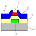
Translated fromKorean도 1은 본 발명의 일 실시예에 따른 박막 트랜지스터의 단면을 나타낸 도이다.1 is a cross-sectional view of a thin film transistor according to an exemplary embodiment of the present invention.
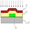
도 2는 본 발명의 일 실시예에 따른 박막 트랜지스터의 제조시 사용되는 플라즈마 질화 공정을 나타낸 도이다.2 is a diagram illustrating a plasma nitridation process used in manufacturing a thin film transistor according to an exemplary embodiment of the present invention.
도 3은 본 발명의 일 실시예에 따른 박막 트랜지스터의 제조시 사용되는 산소 열처리를 나타낸 도이다.3 is a diagram illustrating an oxygen heat treatment used in manufacturing a thin film transistor according to an exemplary embodiment of the present invention.
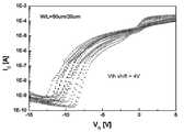
도 4는 본 발명의 일 실시예에 따른 박막 트랜지스터의 트랜스퍼(transfer) 특성을 나타낸 도이다.4 is a diagram illustrating transfer characteristics of a thin film transistor according to an exemplary embodiment of the present invention.
도 5는 본 발명의 일 실시예에 따른 박막 트랜지스터의 아웃풋(output) 특성을 나타낸 도이다.5 is a diagram illustrating output characteristics of a thin film transistor according to an exemplary embodiment of the present invention.
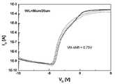
도 6은 본 발명의 일 실시예에 따른 박막 트랜지스터의 트랜스퍼(transfer) 특성을 나타낸 도이다.6 illustrates a transfer characteristic of a thin film transistor according to an exemplary embodiment of the present invention.
도 7은 본 발명의 일 실시예에 따른 박막 트랜지스터의 아웃풋(output) 특성을 나타낸 도이다.7 is a diagram illustrating output characteristics of a thin film transistor according to an exemplary embodiment of the present invention.
<도면의 주요 부분에 대한 부호의 설명><Explanation of symbols for the main parts of the drawings>
10 : 기판 20 : 게이트 전극10
30 : 절연층 40 : 반도체층30: insulating layer 40: semiconductor layer
50 : 소스 전극 60 : 드레인 전극50
본 발명은 박막 트랜지스터 및 이의 제조방법에 관한 것이다. 구체적으로, 본 발명은 박막 트랜지스터에 있어서, 반도체층의 채널 물질로서 Si를 포함하는 산화 아연계 물질을 사용하는 박막 트랜지스터 및 이의 제조방법에 관한 것이다.The present invention relates to a thin film transistor and a method of manufacturing the same. Specifically, the present invention relates to a thin film transistor using a zinc oxide-based material containing Si as a channel material of a semiconductor layer, and a method of manufacturing the same in a thin film transistor.
일반적으로 박막 트랜지스터는 소스(sourse) 전극, 드레인(drain) 전극, 게이트(gate) 전극, 반도체층, 절연층, 기판 등으로 이루어진다.In general, the thin film transistor includes a source electrode, a drain electrode, a gate electrode, a semiconductor layer, an insulating layer, a substrate, and the like.
상기 반도체층의 채널 물질로는 ZnO가 일반적으로 사용되고 있는데, 구체적으로 ZnO에 1족 알칼리(Li, Na) 또는 5족(N, P, As)을 도핑하여 p-형 채널 물질로 사용하는 것이다.ZnO is generally used as a channel material of the semiconductor layer. Specifically, ZnO is doped with group 1 alkali (Li, Na) or group 5 (N, P, As) to be used as a p-type channel material.
그러나, ZnO는 n-형 도판트(dopant)로 작용할 수 있는 산소 공극(oxygen vacancy), Zn 간극(interstitial) 등의 형성 엔탈피가 매우 낮아 자발적으로 생성된 정공 킬러(hole killer)로 작용하기 쉽기 때문에, 반도체층으로서 p-형 도핑이 어려운 문제점이 있다.However, ZnO has a very low enthalpy of formation such as oxygen vacancy and Zn interstitial, which may act as n-type dopants, and thus is likely to act as a spontaneously generated hole killer. As a semiconductor layer, p-type doping is difficult.
또한, 산소 공극(oxygen vacancy), Zn 간극(interstitial) 등의 형성 엔탈피가 낮은 ZnO의 고유한 특성으로 인하여 ZnO 박막 트랜지스터 제조시 강한 n-형의 채널이 형성되고, 문턱전압 및 채널의 이동도 또한 경시 변화하는 불안정한 모습을 보이고 있다.In addition, due to the unique characteristics of ZnO, which have low formation enthalpy such as oxygen vacancy and Zn interstitial, a strong n-type channel is formed in ZnO thin film transistor fabrication, and threshold voltage and channel mobility are also increased. It is unstable, changing over time.
한편, 한국 특허 공개 공보 2004-79516에는 5족(N, P, As, Sb, Bi) 원소 또는 5족 원소의 산화물이 포함된 산화아연 화합물을 사용하여 기판상에 도판트로서 5족 원소가 첨가된 아연산화물 박막을 형성하고, 상기 도판트를 활성화시키는 방법을 기재하고 있으나, 상기 활성화가 용이하지 않다는 단점이 있다.Meanwhile, Korean Patent Laid-Open Publication No. 2004-79516 adds a
따라서, ZnO 박막 트랜지스터 제조시 ZnO 물질 자체만으로는 p-형 도핑이 어려우므로, 1족 알칼리(Li, Na 등) 또는 5족(N, P, As 등)을 이용한 p-형 도핑이 가능한 물질의 개발이 요구되고 있다.Therefore, when the ZnO thin film transistor is manufactured, p-type doping is difficult with only ZnO material itself, and thus, a p-type doping material using group 1 alkali (Li, Na, etc.) or group 5 (N, P, As, etc.) is developed. This is required.
상기의 문제점들을 해결하기 위하여, 본 발명자들은 박막 트랜지스터에 있어서 반도체층의 채널의 n-형 전도도를 낮추고, 질소 도핑을 원활하게 할 수 있는 박막 트랜지스터의 제조방법을 개발하였다.In order to solve the above problems, the present inventors have developed a method of manufacturing a thin film transistor which can reduce the n-type conductivity of the channel of the semiconductor layer and smoothly do the nitrogen in the thin film transistor.
이에 본 발명은 박막 트랜지스터의 제조방법에 있어서, 반도체층의 채널 물질로서 Si를 포함하는 산화 아연계 물질을 사용하는 박막 트랜지스터의 제조방법을 제공하고자 한다.Accordingly, the present invention provides a method of manufacturing a thin film transistor using a zinc oxide-based material containing Si as a channel material of a semiconductor layer.
또한, 본 발명은 박막 트랜지스터의 제조방법에 있어서, 상기 채널 물질의 증착 후 플라즈마 질화 공정, 및 산소 열처리 공정을 거치는 박막 트랜지스터의 제조방법을 제공하고자 한다.In addition, the present invention is to provide a method for manufacturing a thin film transistor through a plasma nitridation process and an oxygen heat treatment process after the deposition of the channel material.
또한, 본 발명은 기판, 게이트 전극, 절연층, 반도체층, 소스 전극 및 드레 인 전극을 포함하는 박막 트랜지스터에 있어서, 상기 반도체층은 Si를 포함하는 산화 아연계 반도체 채널 물질을 포함하는 박막 트랜지스터를 제공하고자 한다.In addition, the present invention is a thin film transistor comprising a substrate, a gate electrode, an insulating layer, a semiconductor layer, a source electrode and a drain electrode, the semiconductor layer comprises a thin film transistor comprising a zinc oxide-based semiconductor channel material containing Si To provide.
구체적으로, 본 발명은Specifically, the present invention
A) 기판에 게이트 전극을 형성하는 게이트 전극 형성 단계;A) forming a gate electrode on the substrate;
B) 상기 기판 및 게이트 전극 위에 절연층을 형성하는 절연층 형성 단계;B) forming an insulating layer on the substrate and the gate electrode;
C) 상기 절연층 위에 채널 물질로서 Si를 포함하는 산화 아연계 물질을 이용하여 반도체층을 형성하는 반도체층 형성 단계; 및C) forming a semiconductor layer using a zinc oxide-based material containing Si as a channel material on the insulating layer; And
D) 상기 반도체층에 연결되도록 소스 전극 및 드레인 전극을 형성하는 소스 및 드레인 전극 형성 단계D) forming a source electrode and a drain electrode to form a source electrode and a drain electrode to be connected to the semiconductor layer
를 포함하는 박막 트랜지스터의 제조방법을 제공한다.It provides a method of manufacturing a thin film transistor comprising a.
또한, 본 발명은 상기 박막 트랜지스터의 제조방법에 있어서, C) 반도체층 형성 단계 이후,In addition, the present invention is a method for manufacturing the thin film transistor, C) after the semiconductor layer forming step,
1) 상기 반도체층에 플라즈마 질화 공정을 이용하여 질소 도핑 처리하는 단계 및1) nitrogen doping the semiconductor layer using a plasma nitridation process; and
2) 상기 질소 도핑 처리된 반도체층을 산소 열처리하는 단계2) oxygen-heat treating the nitrogen-doped semiconductor layer
를 추가로 포함하는 박막 트랜지스터의 제조방법을 제공한다.It provides a method of manufacturing a thin film transistor further comprising.
또한, 본 발명은 기판, 게이트 전극, 절연층, 반도체층, 소스 전극 및 드레인 전극을 포함하는 박막 트랜지스터에 있어서, 상기 반도체층은 Si를 포함하는 산화 아연계 반도체 채널 물질을 포함하는 박막 트랜지스터를 제공한다.The present invention also provides a thin film transistor comprising a substrate, a gate electrode, an insulating layer, a semiconductor layer, a source electrode and a drain electrode, wherein the semiconductor layer comprises a zinc oxide-based semiconductor channel material including Si. do.
이하 본 발명에 대해서 상세히 설명한다.Hereinafter, the present invention will be described in detail.
본 발명은The present invention
A) 기판에 게이트 전극을 형성하는 게이트 전극 형성 단계;A) forming a gate electrode on the substrate;
B) 상기 기판 및 게이트 전극 위에 절연층을 형성하는 절연층 형성 단계;B) forming an insulating layer on the substrate and the gate electrode;
C) 상기 절연층 위에 채널 물질로서 Si를 포함하는 산화 아연계 물질을 이용하여 반도체층을 형성하는 반도체층 형성 단계; 및C) forming a semiconductor layer using a zinc oxide-based material containing Si as a channel material on the insulating layer; And
D) 상기 반도체층에 연결되도록 소스 전극 및 드레인 전극을 형성하는 소스 전극 및 드레인 전극 형성 단계D) forming a source electrode and a drain electrode to form a source electrode and a drain electrode to be connected to the semiconductor layer
를 포함하는 박막 트랜지스터의 제조방법을 제공한다.It provides a method of manufacturing a thin film transistor comprising a.
본 발명에 따른 박막 트랜지스터의 제조방법에 있어서, 상기 A) 게이트 전극 형성 단계의 기판은 박막 트랜지스터를 위한 열역학적 및 기계적 요구사항을 만족시킬 수 있는 유리, 반도체 웨이퍼(semiconductor wafer), 금속 산화물, 세라믹 물질, 플라스틱 등이 사용될 수 있다. 특히, 상기 기판은 유리 또는 플라스틱인 것이 바람직하나, 이에만 한정되는 것은 아니다.In the method of manufacturing a thin film transistor according to the present invention, the substrate of the A) gate electrode forming step is a glass, a semiconductor wafer, a metal oxide, a ceramic material that can satisfy the thermodynamic and mechanical requirements for the thin film transistor , Plastic and the like can be used. In particular, the substrate is preferably glass or plastic, but is not limited thereto.
상기 A)의 게이트 전극 형성 단계는 기판 상에 도전성 물질을 이용한 도전성 물질층 형성 단계 및 상기 도전성 물질층을 패터닝하는 전극 패턴 형성 단계를 포함하는 방법에 의해 수행될 수 있다. 또한, 상기 A)의 게이트 전극 형성 단계는 기판 상에 도전성 물질을 직접 인쇄하여 패터닝하는 방법에 의해서도 수행될 수 있다.The forming of the gate electrode of A) may be performed by a method including forming a conductive material layer using a conductive material on a substrate and forming an electrode pattern for patterning the conductive material layer. In addition, the gate electrode forming step of A) may be performed by a method of directly printing and patterning a conductive material on a substrate.
상기 A) 게이트 전극 형성 단계의 도전성 물질은 탄소, 알루미늄, 바나듐, 크롬, 구리, 아연, 은, 금, 마그네슘, 칼슘, 나트륨, 칼륨, 티타늄, 인듐, 이트륨, 리튬, 가돌리늄, 주석, 납, 금속 유사물(similar metals) 및 이들의 합금; p- 또는 n- 도프된(doped) 실리콘; 산화 아연, 산화 인듐, 인듐 주속 산화물(ITO), 인듐 아연 산화물, 유사 주석 산화물(similar tin oxide) 및 주석 산화물 인듐계 복합 화합물(tin oxide indium-based complex compounds); ZnO : Al, SnO2 : Sb와 같은 산화물과 금속의 혼합물; 폴리(3-메틸티오펜)(poly(3-methylthiophene)), 폴리[3,4-(에틸렌-1,2-디옥시)티오펜](poly[3,4-(ethylene-1,2-dioxy)thiophene]), 폴리피롤(polypyrrole) 및 폴리아닐린과 같은 도전성 고분자 등이 있으나, 이에만 한정되는 것은 아니다.The conductive material of the A) gate electrode forming step is carbon, aluminum, vanadium, chromium, copper, zinc, silver, gold, magnesium, calcium, sodium, potassium, titanium, indium, yttrium, lithium, gadolinium, tin, lead, metal Similar metals and alloys thereof; p- or n- doped silicon; Zinc oxide, indium oxide, indium primary oxide (ITO), indium zinc oxide, similar tin oxide and tin oxide indium-based complex compounds; Mixtures of oxides and metals such as ZnO: Al, SnO2 : Sb; Poly (3-methylthiophene), poly [3,4- (ethylene-1,2-dioxy) thiophene] (poly [3,4- (ethylene-1,2- dioxy) thiophene]), polypyrrole, and a conductive polymer such as polyaniline, and the like, but are not limited thereto.
상기 A) 게이트 전극 형성 단계의 도전성 물질층 형성 단계에서는 화학 증착법(Chemical Vapor Deposition; CVD), 플라즈마 화학 증착법(Plasma-Enhanced Chemical Vapor Deposition; PECVD), 스퍼터링법(Sputtering), 전자빔 증착법(E-beam evaporation), 열 증착법(Thermal evaporation), 레이저 분자빔 증착법(Laser Molecular Beam Epitaxy; L-MBE), 펄스 레이저 증착법(Pulsed Laser Deposition; PLD), 및 원자층 증착법(Atomic layer deposition) 중에서 선택되는 방법을 이용할 수 있다. 도전성 물질층 형성방법은 이에만 한정되는 것은 아니며, 당 기술분야에 알려진 도전성 물질층 형성방법을 모두 적용할 수 있다.In the conductive material layer forming step of the A) gate electrode forming step, chemical vapor deposition (CVD), plasma-enhanced chemical vapor deposition (PECVD), sputtering, and electron beam deposition (E-beam) evaporation, Thermal evaporation, Laser Molecular Beam Epitaxy (L-MBE), Pulsed Laser Deposition (PLD), and Atomic layer deposition It is available. The conductive material layer forming method is not limited thereto, and any conductive method known in the art may be applied.
상기 A) 게이트 전극 형성 단계의 전극 패턴 형성 단계에서는 포토리소그래피법, 오프셋 인쇄법, 실크스크린 인쇄법, 잉크젯 인쇄법, 및 쉐도우 마스 크(Shadow Mask)를 이용한 방법 중에서 선택되는 방법을 이용할 수 있다.In the electrode pattern forming step of the A) gate electrode forming step, a method selected from a photolithography method, an offset printing method, a silkscreen printing method, an inkjet printing method, and a shadow mask may be used.
상기 A) 게이트 전극 형성 단계의 게이트 전극의 두께는 50nm 이상 400nm 이하로 사용되며, 바람직하게는 200nm가 적당하다.The thickness of the gate electrode in the A) gate electrode forming step is used 50nm or more and 400nm or less, preferably 200nm.
본 발명에 따른 박막 트랜지스터의 제조방법에 있어서, 상기 B) 절연층 형성 단계의 절연층으로는 실리콘 산화물, 실리콘 질화물; 폴리이미드, 폴리(2-비닐피리딘), 폴리(4-비닐페놀), 폴리메틸 메타크릴레이트와 같은 플라스틱 절연체 등이 있으나, 이에만 한정되는 것은 아니다.In the method of manufacturing a thin film transistor according to the present invention, the insulating layer of the step B) forming an insulating layer may include silicon oxide, silicon nitride; Plastic insulators such as polyimide, poly (2-vinylpyridine), poly (4-vinylphenol), polymethyl methacrylate, and the like, but are not limited thereto.
상기 B)의 절연층 형성 단계에서는 화학 증착법(Chemical Vapor Deposition; CVD), 플라즈마 화학 증착법(Plasma-Enhanced Chemical Vapor Deposition; PECVD), 스퍼터링법(Sputtering), 전자빔 증착법(E-beam evaporation), 열 증착법(Thermal evaporation), 레이저 분자빔 증착법(Laser Molecular Beam Epitaxy; L-MBE), 펄스 레이저 증착법(Pulsed Laser Deposition; PLD), 및 원자층 증착법(Atomic layer deposition) 중에서 선택되는 방법을 이용할 수 있다. 절연층 형성방법은 이에만 한정되는 것은 아니며, 당 기술분야에 알려진 절연층 형성방법을 모두 적용할 수 있다.In the step of forming the insulating layer of B), Chemical Vapor Deposition (CVD), Plasma-Enhanced Chemical Vapor Deposition (PECVD), Sputtering, E-beam evaporation, and Thermal Vapor Deposition (Thermal evaporation), Laser Molecular Beam Epitaxy (L-MBE), Pulsed Laser Deposition (PLD), and atomic layer deposition (Atomic layer deposition) can be used. The method of forming the insulating layer is not limited thereto, and any method of forming an insulating layer known in the art may be applied.
상기 B) 절연층 형성 단계의 절연층의 두께는 100nm 이상 500nm 이하로 사용되며, 바람직하게는 300nm가 적당하다.The thickness of the insulating layer of the B) insulating layer forming step is used at 100nm or more and 500nm or less, preferably 300nm.
본 발명에 따른 박막 트랜지스터의 제조방법에 있어서, 상기 C) 반도체층 형성 단계의 채널 물질로 이용되는 Si를 포함하는 산화 아연계 물질은 ZnO, ZnO : Al, ZnO : Ga, ZnO : In, 또는 이들의 복합 산화물에 0 초과 30 몰% 이하의 Si를 포함하는 물질인 것이 바람직하나, 이에만 한정되는 것은 아니다.In the method of manufacturing a thin film transistor according to the present invention, the C) zinc oxide-based material including Si used as the channel material in the semiconductor layer forming step is ZnO, ZnO: Al, ZnO: Ga, ZnO: In, or these It is preferable that it is a material containing more than 0 and 30 mol% or less Si in the complex oxide of, but it is not limited only to this.
본 발명에 따른 박막 트랜지스터의 제조방법에 있어서, 상기 C) 반도체층 형성 단계의 채널 물질로 이용되는 Si를 포함하는 산화 아연계 물질은 ZnO-In2O3-SiO2인 것이 더욱 바람직하다.In the method of manufacturing a thin film transistor according to the present invention, the C) zinc oxide-based material including Si used as the channel material in the semiconductor layer forming step is more preferably ZnO—In2 O3 —SiO2 .
상기 ZnO-In2O3-SiO2에 있어서, Si의 함량은 0 초과 30 몰% 이하, Zn의 함량은 0 초과 66 몰% 이하, 및 In의 함량은 0 초과 33 몰% 이하인 것이 바람직하나, 이에만 한정되는 것은 아니다. 상기 ZnO-In2O3-SiO2에 있어서, Si의 함량이 증가하는 경우에는 반도체층의 전도도가 크게 감소하여 반도체층의 역할을 상실할 수 있고, In의 함량이 증가하는 경우에는 전도도가 크게 증가하여 전극과 같은 역할을 할 수 있다.In the ZnO—In2 O3 —SiO2 , the content of Si is more than 0 and 30 mol% or less, the content of Zn is more than 0 and 66 mol% or less, and the content of In is more than 0 and 33 mol% or less, It is not limited only to this. In the ZnO—In2 O3 —SiO2 , when the content of Si is increased, the conductivity of the semiconductor layer may be greatly reduced, thereby losing the role of the semiconductor layer, and when the content of In is increased, the conductivity is large. It can increase and act as an electrode.
또한, ZnO-In2O3-SiO2에 있어서, Zn : In : Si의 몰% 비는 1 : 1 : 1인 것이 바람직하나, 이에만 한정되는 것은 아니다.In ZnO-In2 O3 -SiO2 , the mole% ratio of Zn: In: Si is preferably 1: 1: 1, but is not limited thereto.
상기 C) 반도체층 형성 단계의 채널 물질로 이용되는 Si를 포함하는 산화 아연계 물질은 그 단독으로도 사용할 수 있을 뿐 아니라, Si를 포함하는 산화 아연계 물질에 주기율표 1족 또는 5족 물질을 첨가하여 사용하는 것도 가능하다. 상기 1족 물질은 Li 또는 Na가 바람직하고, 상기 5족 물질은 N, P, 또는 As가 바람직하나, 이에만 한정되는 것은 아니다.The zinc oxide-based material including Si used as the channel material of the semiconductor layer forming step may be used alone, and the
상기 C) 반도체층 형성 단계의 채널 물질은 스퍼터링(sputtering) 방법, 화학 증착법(Chemical Vapor Deposition; CVD), 원자층 증착법(Atomic Layer Deposition; ALD), 펄스 레이저 증착법(Pulsed Laser Deposition; PLD), 레이저 분자빔 증착법(Laser Molecular Beam Epitaxy; L-MBE), 전자빔 증착법(E-beam evaporation), 이온빔 증착법(Ion-beam evaporation) 등의 방법을 이용하여 반도체층으로 증착할 수 있으며, Si가 함유되어 있으므로 주기율표 5족 도판트들이 ZnO에 직접 도핑되는 것보다 쉽게 도핑될 수 있다. 또한, 반도체층의 카운터(counter) 도핑이 용이할 수 있다.The channel material of the C) semiconductor layer forming step is a sputtering method, chemical vapor deposition (CVD), atomic layer deposition (ALD), pulsed laser deposition (PLD), laser It can be deposited into a semiconductor layer by using a method such as molecular beam deposition (L-MBE), electron beam evaporation (I-beam evaporation), ion beam evaporation (Ion-beam evaporation), and because it contains
상기 C) 반도체층 형성 단계의 반도체층의 두께는 10nm 이상 200nm 이하로 사용 가능하며, 바람직하게는 10nm 이상 100nm 이하가 적당하다.The thickness of the semiconductor layer of the C) semiconductor layer forming step may be used in more than 10nm 200nm, preferably 10nm or more and 100nm or less.
상기 D)의 소스 전극 및 드레인 전극 형성 단계는 상기 절연층과 반도체층이 함께 커버되도록 상기 절연층 및 반도체층 위에 도전성 물질을 이용한 도전성 물질층 형성 단계 및 상기 도전성 물질층을 패터닝하는 전극 패턴 형성 단계를 포함하는 방법에 의해 수행될 수 있다. 또한, 상기 D)의 소스 전극 및 드레인 전극 형성 단계는 절연층 및 반도체층 위에 도전성 물질을 직접 인쇄하여 패터닝하는 방법에 의해서도 수행될 수 있다.The forming of the source electrode and the drain electrode of D) includes forming a conductive material layer using a conductive material on the insulating layer and the semiconductor layer so as to cover the insulating layer and the semiconductor layer together, and forming an electrode pattern to pattern the conductive material layer. It may be performed by a method comprising a. In addition, the forming of the source electrode and the drain electrode of D) may be performed by a method of directly printing and patterning a conductive material on the insulating layer and the semiconductor layer.
상기 D) 소스 전극 및 드레인 전극 형성 단계의 도전성 물질은 탄소, 알루미늄, 바나듐, 크롬, 구리, 아연, 은, 금, 마그네슘, 칼슘, 나트륨, 칼륨, 티타늄, 인듐, 이트륨, 리튬, 가돌리늄, 주석, 납, 네오디뮴(neodymium), 백금, 금속 유사물(similar metals) 및 이들의 합금; p- 또는 n- 도프된(doped) 실리콘; 산화아연, 산화인듐, 인듐 주석 산화물(ITO), 인듐 아연 산화물, 주석 유사 산화물(similar tin oxide) 및 주석 산화물 인듐계 복합 화합물(tin oxide indium-based complex compounds); ZnO : Al, SnO2 : Sb와 같은 산화물과 금속의 혼합물; 폴리(3-메틸티오펜)(poly(3-methylthiophene)), 폴리[3,4-(에틸렌-1,2-디옥시)티오펜] (poly[3,4-(ethylene-1,2-dioxy) thiophene]), 폴리피롤(polypyrrole) 및 폴리아닐린(polyaniline)과 같은 도전성 고분자 등이 있으나, 이에만 한정되는 것은 아니다.The conductive material of the source electrode and drain electrode forming step is carbon, aluminum, vanadium, chromium, copper, zinc, silver, gold, magnesium, calcium, sodium, potassium, titanium, indium, yttrium, lithium, gadolinium, tin, Lead, neodymium, platinum, similar metals and alloys thereof; p- or n- doped silicon; Zinc oxide, indium oxide, indium tin oxide (ITO), indium zinc oxide, similar tin oxide and tin oxide indium-based complex compounds; Mixtures of oxides and metals such as ZnO: Al, SnO2 : Sb; Poly (3-methylthiophene), poly [3,4- (ethylene-1,2-dioxy) thiophene] (poly [3,4- (ethylene-1,2- dioxy) thiophene]), polypyrrole and polyaniline such as conductive polymers, but are not limited thereto.
상기 D) 소스 전극 및 드레인 전극 형성 단계의 도전성 물질층 형성 단계에서는 화학 증착법(Chemical Vapor Deposition; CVD), 플라즈마 화학 증착법(Plasma-Enhanced Chemical Vapor Deposition; PECVD), 스퍼터링법(Sputtering), 전자빔 증착법(E-beam evaporation), 열 증착법(Thermal evaporation), 레이저 분자빔 증착법(Laser Molecular Beam Epitaxy; L-MBE), 펄스 레이저 증착법(Pulsed Laser Deposition; PLD), 및 원자층 증착법(Atomic layer deposition) 중에서 선택되는 방법을 이용할 수 있다. 도전성 물질층 형성방법은 이에만 한정되는 것은 아니며, 당 기술분야에 알려진 도전성 물질층 형성방법을 모두 적용할 수 있다.In the conductive material layer forming step of forming the source electrode and the drain electrode, the chemical vapor deposition (CVD), the plasma-enhanced chemical vapor deposition (PECVD), the sputtering method, the electron beam deposition method ( Choose from E-beam evaporation, Thermal evaporation, Laser Molecular Beam Epitaxy (L-MBE), Pulsed Laser Deposition (PLD), and Atomic layer deposition Can be used. The conductive material layer forming method is not limited thereto, and any conductive method known in the art may be applied.
상기 D) 소스 전극 및 드레인 전극 형성 단계의 전극 패턴 형성 단계에서는 포토리소그래피법, 오프셋 인쇄법, 실크스크린 인쇄법, 잉크젯 인쇄법, 및 쉐도우 마스크(Shadow Mask)를 이용한 방법 중에서 선택되는 방법을 이용할 수 있다.In the electrode pattern forming step of forming the source electrode and the drain electrode, a method selected from a photolithography method, an offset printing method, a silkscreen printing method, an inkjet printing method, and a shadow mask method may be used. have.
상기 D) 소스 전극 및 드레인 전극 형성 단계의 소스 전극 및 드레인 전극의 두께는 50nm 이상 400nm 이하로 사용 가능하며, 바람직하게는 200nm가 적당하다.The thickness of the source electrode and the drain electrode in the step D) of forming the source electrode and the drain electrode may be 50 nm or more and 400 nm or less, preferably 200 nm.
본 발명에 따른 박막 트랜지스터의 제조방법은 반도체층의 채널 물질로서 Si 를 포함하는 산화 아연계 물질을 사용하기 때문에, 반도체층의 채널의 n-형 전도도를 낮추고, 반도체층에 질소 도핑을 원할하게 할 수 있다.Since the method for manufacturing a thin film transistor according to the present invention uses a zinc oxide-based material including Si as the channel material of the semiconductor layer, it is possible to reduce the n-type conductivity of the channel of the semiconductor layer and to smooth nitrogen doping of the semiconductor layer. Can be.
또한, 본 발명은 상기 박막 트랜지스터의 제조방법에 있어서, C) 반도체층 형성 단계 이후,In addition, the present invention is a method for manufacturing the thin film transistor, C) after the semiconductor layer forming step,
1) 상기 반도체층에 플라즈마 질화 공정을 이용하여 질소 도핑 처리하는 단계 및1) nitrogen doping the semiconductor layer using a plasma nitridation process; and
2) 상기 질소 도핑 처리된 반도체층을 산소 열처리하는 단계2) oxygen-heat treating the nitrogen-doped semiconductor layer
를 추가로 수행할 수 있다.Can be performed further.
본 발명에 따른 박막 트랜지스터의 제조방법에 있어서, 상기 1) 질소 도핑 처리하는 단계의 플라즈마 질화 공정은 박막 트랜지스터의 반도체층 내에 N을 주입시키는 역할을 하고, 상기 2) 산소 열처리 단계는 박막 트랜지스터의 반도체층 내에 주입된 N을 더욱 단단히 결합시키는 역할을 한다.In the method of manufacturing a thin film transistor according to the present invention, the plasma nitriding process of the step 1) nitrogen doping serves to inject N into the semiconductor layer of the thin film transistor, and the step 2) the oxygen heat treatment is a semiconductor of the thin film transistor. It serves to more tightly bond the N injected into the layer.
상기 1) 질소 도핑 처리하는 단계의 플라즈마 질화 공정은 NH3, N2O, N2, NO, 및 NF3 중에서 선택된 1종 이상을 이용할 수 있으나, 이에만 한정되는 것은 아니다.The plasma nitriding process of the step 1) of nitrogen doping may use one or more selected from NH3 , N2 O, N2 , NO, and NF3 , but is not limited thereto.
상기 플라즈마 질화 공정을 이용한 질소 도핑 처리는 특별히 제한되는 것은 아니나, 바람직하게는 200 ~ 500℃의 온도에서 60분 이하의 시간 동안 수행될 수 있다.Nitrogen doping treatment using the plasma nitridation process is not particularly limited, but may be preferably performed for a time of 60 minutes or less at a temperature of 200 ~ 500 ℃.
상기 플라즈마 질화 공정을 이용한 질소 도핑 처리의 구체적인 일 실시예로서 사용 압력 1mTorr, 플라즈마 전력(plasma power) 200W, 온도 300℃, 3분을 기본 공정으로 실시할 수 있고, 이 때 사용 가스는 N2 1050sccm, NH3 80sccm이 주입될 수 있다. 또한, 도핑 농도는 플라즈마 전력(plasma power)으로 조절할 수 있으며, ICP(Inductively Coupled Plasma) 타입의 플라즈마 도핑이 더욱 바람직하다.As a specific example of the nitrogen doping treatment using the plasma nitridation process, a pressure of 1 mTorr, a plasma power of 200 W, a temperature of 300 ° C., and 3 minutes may be performed as a basic process, and the gas used may be N2 1050 sccm. NH3 80 sccm may be injected. In addition, the doping concentration may be controlled by plasma power, and plasma doping of ICP (Inductively Coupled Plasma) type is more preferable.
상기 2)의 산소 열처리는 산소분위기 하에서 급속 열처리(Rapid Thermal Annealing; RTA)하는 방법이 이용될 수 있다. 상기 급속 열처리는 기판에 가해지는 온도 변화, 즉 온도 램핑(ramping) 속도가 빠른 열처리 방식을 통칭하여 일컫는다.Oxygen heat treatment of 2) may be a method of rapid thermal annealing (RTA) under an oxygen atmosphere. The rapid heat treatment is referred to collectively as a heat treatment method in which a temperature change applied to a substrate, that is, a temperature ramping speed is high.
상기 산소 열처리의 구체적인 일 실시예로서 200℃ 이상 500℃ 이하의 온도에서 1시간 이하의 시간 동안 산소분위기 하에서 급속 열처리를 할 수 있으나, 이에만 한정되는 것은 아니다.As a specific example of the oxygen heat treatment, rapid heat treatment may be performed under an oxygen atmosphere at a temperature of 200 ° C. or more and 500 ° C. or less for 1 hour or less, but is not limited thereto.
본 발명에 따른 박막 트랜지스터의 제조방법은 반도체층의 채널 물질로서 Si를 포함하는 산화 아연계를 사용하고, 상기 채널 물질의 증착 후 플라즈마 질화 공정 및 산소 열처리 공정을 거치는 박막 트랜지스터의 제조방법을 사용함으로써, 아연 산화물 반도체의 문제점인 산소 공극과 아연 간극에 의한 자발적인 n-형 도판트들을 제거하고, 동시에 5족 p-형 도판트인 N이 Si과 결합하여 채널로서 적합한 전도도를 형성하고 유지시킬 수 있다.The method of manufacturing a thin film transistor according to the present invention uses a zinc oxide-based containing Si as the channel material of the semiconductor layer, and by using a method of manufacturing a thin film transistor that undergoes a plasma nitridation process and an oxygen heat treatment process after deposition of the channel material. In addition, spontaneous n-type dopants caused by oxygen voids and zinc gaps, which are a problem of zinc oxide semiconductors, can be removed, and at the same time, the Group 5 p-type dopant N can be combined with Si to form and maintain a suitable conductivity as a channel.
또한, 본 발명은 기판, 게이트 전극, 절연층, 반도체층, 소스 전극 및 드레인 전극을 포함하는 박막 트랜지스터에 있어서, 상기 반도체층은 Si를 포함하는 산화 아연계 반도체 채널 물질을 포함하는 박막 트랜지스터를 제공한다.The present invention also provides a thin film transistor comprising a substrate, a gate electrode, an insulating layer, a semiconductor layer, a source electrode and a drain electrode, wherein the semiconductor layer comprises a zinc oxide-based semiconductor channel material including Si. do.
본 발명에 있어서, 상기 반도체층은 반도체층 형성 후, 플라즈마 질화 공정 및 산소 열처리를 순차적으로 받은 것일 수 있다.In the present invention, the semiconductor layer may be subjected to a plasma nitridation process and oxygen heat treatment sequentially after the semiconductor layer is formed.
상기 Si를 포함하는 산화 아연계 물질은 박막 트랜지스터의 제조방법에서 기술한 바와 같이 ZnO, ZnO : Al, ZnO : Ga, ZnO : In, 또는 이들의 복합 산화물에 0 초과 30 몰% 이하의 Si를 포함하는 물질인 것이 바람직하나, 이에만 한정되는 것은 아니다.The zinc oxide-based material including Si includes more than 0 and 30 mol% or less Si in ZnO, ZnO: Al, ZnO: Ga, ZnO: In, or a composite oxide thereof as described in the method of manufacturing a thin film transistor. It is preferable that the substance is not limited thereto.
또한, 상기 반도체층은 Si를 포함하는 산화 아연계 물질 단독, 또는 Si를 포함하는 산화 아연계 물질에 주기율표 1족 또는 5족 물질을 첨가한 채널 물질을 이용하여 형성될 수 있다.In addition, the semiconductor layer may be formed using a zinc oxide-based material including Si alone or a channel material in which a
이하 본 발명의 이해를 돕기 위해 바람직한 실시예를 제시한다. 그러나, 하기의 실시예는 본 발명을 보다 쉽게 이해하기 위하여 제공되는 것일 뿐, 이에 의해 본 발명의 내용이 한정되는 것은 아니다.Hereinafter, preferred examples are provided to help understanding of the present invention. However, the following examples are provided only for the purpose of easier understanding of the present invention, and the present invention is not limited thereto.
<<실시예Example>>
본 발명의 일 실시예에 따른 박막 트랜지스터 제조방법은 1) 기판(10)에 게이트 전극(20)을 형성하는 게이트 전극 형성 단계; 2) 상기 기판 및 게이트 전극(20) 위에 절연층(30)을 형성하는 절연층 형성 단계; 3) 상기 절연층(30) 위에 채널 물질로서 Si를 포함하는 산화 아연계 물질을 이용하여 반도체층(40)을 형성하는 반도체층 형성 단계; 4) 상기 반도체층(40)에 플라즈마 질화 공정을 이용하여 질소 도핑 처리하는 단계; 5) 상기 질소 도핑 처리된 반도체층(40)을 산소 열처리하는 단계; 및 6) 상기 산소 열처리된 반도체층(40)에 연결되도록 소스 전극(50) 및 드레인 전극(60)을 형성하는 소스 전극 및 드레인 전극 형성 단계를 포함한다.According to one or more exemplary embodiments, a method of manufacturing a thin film transistor includes: 1) forming a
1) 단계에서는, 스퍼터링법으로 유리 기판(10) 상에 인듐주석산화막(ITO)을 증착한 후, 포토리소그래피법을 사용하여패터닝하여 복수의 게이트 배선과 게이트 전극(20)을 형성하였다.In step 1), an indium tin oxide film (ITO) is deposited on the
2) 단계에서는, 스퍼터링 방법으로 게이트 전극 배선을 형성하고 PECVD법을 이용하여 게이트 전극(20)이 형성된 유리 기판(10)의 상부면에 절연층(30)을 형성하였다. 여기서, 게이트 절연층(30)은 SiNx로 형성될 수 있다.In step 2), the gate electrode wiring was formed by the sputtering method, and the insulating
3) 단계에서는, 채널 물질로서 ZnO-In2O3-SiO2를(몰% 비 Zn : In : Si = 1 : 1 : 1) 이용하고 스퍼터링법으로 반도체층(40)을 형성하였다.In step 3), the
4) 단계에서는, NH3를 이용하여 반도체층(40)을 플라즈마 전력(plasma power) 200W, 온도 300℃, 압력 1mTorr으로, 3분 동안 플라즈마 질소 도핑 처리하였다.In step 4), the
5) 단계에서는 질소 도핑 처리된 반도체층(40)을 급속 산소 열처리(RTO)하였다.In step 5), the nitrogen doped
6) 단계에서는 스퍼터링법으로 반도체층(40)의 상부와 절연층(30)의 상부에 몰리브덴층을 증착한 후, 포토리소그래피법으로패터닝하여 게이트 배선과 교차하는 방향으로 데이터 배선을 형성하고, 소스 전극(50)과 드레인 전극(60)을 형성하였다.In the step 6), a molybdenum layer is deposited on the upper portion of the
본 발명에 따른 박막 트랜지스터의 제조방법의 구체적인 일 실시예로서, 반도체층의 채널 물질로 ZnO-In2O3-SiO2를 사용하고, 채널 물질 증착 후 플라즈마 질 화 공정 및 산소 열처리 공정을 거친 박막 트랜지스터의 특성을 도 6 및 도 7에 나타내었다. 또한, 플라즈마 질화 공정을 거치지 않고, 산소 열처리 공정을 거친 박막 트랜지스터의 특성을 도 4 및 도 5에 나타내었다.As a specific embodiment of the method for manufacturing a thin film transistor according to the present invention, ZnO—In2 O3 —SiO2 is used as a channel material of the semiconductor layer, and the thin film is subjected to a plasma nitridation process and an oxygen heat treatment process after deposition of the channel material. The characteristics of the transistors are shown in FIGS. 6 and 7. 4 and 5 show the characteristics of the thin film transistor which undergoes the oxygen heat treatment process without undergoing the plasma nitridation process.
도 4는 플라즈마 질화 공정을 거치지 않고, 산소 열처리 공정을 거친 박막 트랜지스터의 트랜스퍼(transfer) 특성을 나타낸 도로서, 4V 정도의 문턱전압 이동이 발생됨을 알 수 있고, 도 5는 플라즈마 질화 공정을 거치지 않고, 산소 열처리 공정을 거친 박막 트랜지스터의 아웃풋(output) 특성을 나타낸 도로서, 박막 트랜지스터의 아웃풋(output) 특성이 포화되지 않고 VD(드레인 전압) 증가에 따라 계속 상승하는 결과가 나타남을 알 수 있다.FIG. 4 is a diagram illustrating transfer characteristics of a thin film transistor that is subjected to an oxygen heat treatment process without undergoing a plasma nitridation process, and it can be seen that a threshold voltage shift of about 4V occurs. FIG. 5 is not subjected to a plasma nitridation process. As a diagram showing the output characteristics of a thin film transistor that has undergone an oxygen heat treatment process, it can be seen that the output characteristics of the thin film transistor do not saturate and continue to rise as the VD (drain voltage) increases. .
반면에, 도 6은 본 발명에 따른 플라즈마 질화 공정 및 산소 열처리 공정을 거친 박막 트랜지스터의 트랜스퍼(transfer) 특성을 나타낸 도로서, 0.75V 정도의 문턱전압 이동이 발생됨을 알 수 있고, 도 7은 본 발명에 따른 플라즈마 질화 공정 및 산소 열처리 공정을 거친 박막 트랜지스터의 아웃풋(output) 특성을 나타낸 도로서, 박막 트랜지스터의 아웃풋(output) 특성이 VD(드레인 전압) 증가에 따라 포화되어 안정되는 결과가 나타남을 알 수 있다.On the other hand, Figure 6 is a diagram showing the transfer (transfer) characteristics of the thin film transistors through the plasma nitridation process and oxygen heat treatment process according to the present invention, it can be seen that the threshold voltage shift of about 0.75V occurs, Figure 7 The output characteristics of the thin film transistors which have been subjected to the plasma nitridation process and the oxygen heat treatment process according to the present invention. The output characteristics of the thin film transistors are saturated and stabilized as VD (drain voltage) increases. It can be seen.
도 4 내지 도 7에 있어서, ID는 드레인 전류, VG는 게이트 전압, VD는 드레인 전압, 및 W/L은 채널의 폭과 길이를 나타낸다.4 to 7, ID represents a drain current, VG represents a gate voltage, VD represents a drain voltage, and W / L represents a width and a length of a channel.
본 발명은 박막 트랜지스터의 제조방법에 있어서, 반도체층의 채널 물질로서 Si를 포함하는 산화 아연계 물질을 사용하는 박막 트랜지스터의 제조방법 및 상기 채널 물질 증착 후 플라즈마 질화 공정 및 산소 열처리 공정을 거치는 박막 트랜지스터의 제조방법을 사용함으로써, 반도체층의 채널의 n-형 전도도를 낮추고, 반도체층에 질소 도핑을 원할하게 할 수 있다.In the method of manufacturing a thin film transistor, a thin film transistor using a zinc oxide-based material including Si as a channel material of a semiconductor layer, and a thin film transistor subjected to plasma nitridation process and oxygen heat treatment process after deposition of the channel material By using the manufacturing method of, the n-type conductivity of the channel of the semiconductor layer can be lowered, and nitrogen doping can be smoothed in the semiconductor layer.
Claims (33)
Translated fromKoreanPriority Applications (6)
| Application Number | Priority Date | Filing Date | Title |
|---|---|---|---|
| KR20070040328AKR100982395B1 (en) | 2007-04-25 | 2007-04-25 | Thin film transistor and method for manufacturing same |
| JP2010506069AJP5312448B2 (en) | 2007-04-25 | 2008-04-25 | Thin film transistor and manufacturing method thereof |
| PCT/KR2008/002376WO2008133456A1 (en) | 2007-04-25 | 2008-04-25 | Thin film transistor and method for preparing the same |
| US12/451,051US8258023B2 (en) | 2007-04-25 | 2008-04-25 | Thin film transistor and method for preparing the same |
| CN2008800134314ACN101669209B (en) | 2007-04-25 | 2008-04-25 | Thin film field effect transistor and its preparation method |
| US13/566,833US9130045B2 (en) | 2007-04-25 | 2012-08-03 | Thin film transistor and method for preparing the same |
Applications Claiming Priority (1)
| Application Number | Priority Date | Filing Date | Title |
|---|---|---|---|
| KR20070040328AKR100982395B1 (en) | 2007-04-25 | 2007-04-25 | Thin film transistor and method for manufacturing same |
Publications (2)
| Publication Number | Publication Date |
|---|---|
| KR20080095603A KR20080095603A (en) | 2008-10-29 |
| KR100982395B1true KR100982395B1 (en) | 2010-09-14 |
Family
ID=39925854
Family Applications (1)
| Application Number | Title | Priority Date | Filing Date |
|---|---|---|---|
| KR20070040328AActiveKR100982395B1 (en) | 2007-04-25 | 2007-04-25 | Thin film transistor and method for manufacturing same |
Country Status (5)
| Country | Link |
|---|---|
| US (2) | US8258023B2 (en) |
| JP (1) | JP5312448B2 (en) |
| KR (1) | KR100982395B1 (en) |
| CN (1) | CN101669209B (en) |
| WO (1) | WO2008133456A1 (en) |
Cited By (1)
| Publication number | Priority date | Publication date | Assignee | Title |
|---|---|---|---|---|
| KR101412408B1 (en) | 2012-12-17 | 2014-06-27 | 경희대학교 산학협력단 | Transparent Thin Film Transitor |
Families Citing this family (50)
| Publication number | Priority date | Publication date | Assignee | Title |
|---|---|---|---|---|
| JP3410607B2 (en) | 1996-04-23 | 2003-05-26 | 新日本製鐵株式会社 | Continuous casting method and immersion nozzle for continuous casting |
| KR101150142B1 (en)* | 2006-04-06 | 2012-06-11 | 어플라이드 머티어리얼스, 인코포레이티드 | Reactive sputtering zinc oxide transparent conductive oxides onto large area substrates |
| US8058096B2 (en)* | 2007-07-31 | 2011-11-15 | Hewlett Packard Development Company, L.P. | Microelectronic device |
| EP2183780A4 (en) | 2007-08-02 | 2010-07-28 | Applied Materials Inc | THIN FILM TRANSISTORS USING THIN FILM SEMICONDUCTOR MATERIALS |
| JP5393058B2 (en)* | 2007-09-05 | 2014-01-22 | キヤノン株式会社 | Field effect transistor |
| US8980066B2 (en)* | 2008-03-14 | 2015-03-17 | Applied Materials, Inc. | Thin film metal oxynitride semiconductors |
| US8143093B2 (en)* | 2008-03-20 | 2012-03-27 | Applied Materials, Inc. | Process to make metal oxide thin film transistor array with etch stopping layer |
| US8258511B2 (en)* | 2008-07-02 | 2012-09-04 | Applied Materials, Inc. | Thin film transistors using multiple active channel layers |
| JP5538797B2 (en)* | 2008-12-12 | 2014-07-02 | キヤノン株式会社 | Field effect transistor and display device |
| TWI501319B (en) | 2008-12-26 | 2015-09-21 | Semiconductor Energy Lab | Semiconductor device and manufacturing method thereof |
| KR101648927B1 (en) | 2009-01-16 | 2016-08-17 | 가부시키가이샤 한도오따이 에네루기 켄큐쇼 | Semiconductor device and manufacturing method thereof |
| US8492756B2 (en) | 2009-01-23 | 2013-07-23 | Semiconductor Energy Laboratory Co., Ltd. | Semiconductor device and method for manufacturing the same |
| US8367486B2 (en) | 2009-02-05 | 2013-02-05 | Semiconductor Energy Laboratory Co., Ltd. | Transistor and method for manufacturing the transistor |
| US8174021B2 (en)* | 2009-02-06 | 2012-05-08 | Semiconductor Energy Laboratory Co., Ltd. | Semiconductor device and method of manufacturing the semiconductor device |
| US8704216B2 (en)* | 2009-02-27 | 2014-04-22 | Semiconductor Energy Laboratory Co., Ltd. | Semiconductor device and manufacturing method thereof |
| US8450144B2 (en)* | 2009-03-26 | 2013-05-28 | Semiconductor Energy Laboratory Co., Ltd. | Semiconductor device and method for manufacturing the same |
| TWI489628B (en)* | 2009-04-02 | 2015-06-21 | Semiconductor Energy Lab | Semiconductor device and method of manufacturing same |
| TWI535023B (en)* | 2009-04-16 | 2016-05-21 | 半導體能源研究所股份有限公司 | Semiconductor device and method of manufacturing same |
| WO2010122274A1 (en)* | 2009-04-24 | 2010-10-28 | Panasonic Corporation | Oxide semiconductor |
| KR102011616B1 (en)* | 2009-06-30 | 2019-08-16 | 가부시키가이샤 한도오따이 에네루기 켄큐쇼 | Method for manufacturing semiconductor device |
| KR101810699B1 (en) | 2009-06-30 | 2018-01-25 | 가부시키가이샤 한도오따이 에네루기 켄큐쇼 | Method for manufacturing semiconductor device |
| KR101732859B1 (en) | 2009-06-30 | 2017-05-04 | 가부시키가이샤 한도오따이 에네루기 켄큐쇼 | Method for manufacturing semiconductor device |
| KR102503687B1 (en) | 2009-07-03 | 2023-02-27 | 가부시키가이샤 한도오따이 에네루기 켄큐쇼 | Method for manufacturing semiconductor device |
| JP5663214B2 (en)* | 2009-07-03 | 2015-02-04 | 株式会社半導体エネルギー研究所 | Method for manufacturing semiconductor device |
| CN102640294B (en)* | 2009-09-24 | 2014-12-17 | 应用材料公司 | Methods of fabricating metal oxide or metal oxynitride TFTs using wet process for source-drain metal etch |
| US8840763B2 (en)* | 2009-09-28 | 2014-09-23 | Applied Materials, Inc. | Methods for stable process in a reactive sputtering process using zinc or doped zinc target |
| CN102598279B (en) | 2009-11-06 | 2015-10-07 | 株式会社半导体能源研究所 | Semiconductor device |
| CN102598284B (en)* | 2009-11-06 | 2015-04-15 | 株式会社半导体能源研究所 | Semiconductor device |
| KR20110056127A (en) | 2009-11-20 | 2011-05-26 | 삼성전자주식회사 | Semiconductor manufacturing method for transistor and manufacturing method of transistor |
| KR101370301B1 (en)* | 2009-11-20 | 2014-03-05 | 가부시키가이샤 한도오따이 에네루기 켄큐쇼 | Method for manufacturing semiconductor device |
| KR101802406B1 (en) | 2009-11-27 | 2017-11-28 | 가부시키가이샤 한도오따이 에네루기 켄큐쇼 | Semiconductor device and method for manufacturing the same |
| KR20120102748A (en)* | 2009-12-11 | 2012-09-18 | 가부시키가이샤 한도오따이 에네루기 켄큐쇼 | Field effect transistor |
| WO2011108382A1 (en)* | 2010-03-05 | 2011-09-09 | Semiconductor Energy Laboratory Co., Ltd. | Method for manufacturing semiconductor device |
| KR102114012B1 (en) | 2010-03-05 | 2020-05-22 | 가부시키가이샤 한도오따이 에네루기 켄큐쇼 | Display device |
| JP5852793B2 (en)* | 2010-05-21 | 2016-02-03 | 株式会社半導体エネルギー研究所 | Method for manufacturing liquid crystal display device |
| KR20130077839A (en)* | 2010-05-21 | 2013-07-09 | 가부시키가이샤 한도오따이 에네루기 켄큐쇼 | Semiconductor device and method of manufacturing the same |
| WO2012029596A1 (en) | 2010-09-03 | 2012-03-08 | Semiconductor Energy Laboratory Co., Ltd. | Method for manufacturing semiconductor device |
| TWI555205B (en) | 2010-11-05 | 2016-10-21 | 半導體能源研究所股份有限公司 | Semiconductor device and method of manufacturing semiconductor device |
| US9478668B2 (en) | 2011-04-13 | 2016-10-25 | Semiconductor Energy Laboratory Co., Ltd. | Oxide semiconductor film and semiconductor device |
| JP6104522B2 (en) | 2011-06-10 | 2017-03-29 | 株式会社半導体エネルギー研究所 | Semiconductor device |
| KR102504604B1 (en) | 2011-09-29 | 2023-02-27 | 가부시키가이샤 한도오따이 에네루기 켄큐쇼 | Semiconductor device |
| JP6082562B2 (en)* | 2011-10-27 | 2017-02-15 | 株式会社半導体エネルギー研究所 | Semiconductor device |
| CN102751240B (en)* | 2012-05-18 | 2015-03-11 | 京东方科技集团股份有限公司 | Thin film transistor array substrate, manufacturing method thereof, display panel and display device |
| KR20150111550A (en)* | 2014-03-25 | 2015-10-06 | 삼성디스플레이 주식회사 | Thin film transistor array panel and method of manufacturing the same |
| CN104167448B (en)* | 2014-08-05 | 2017-06-30 | 京东方科技集团股份有限公司 | Thin film transistor (TFT) and preparation method thereof, array base palte and display device |
| CN104538457A (en)* | 2015-01-15 | 2015-04-22 | 京东方科技集团股份有限公司 | Thin film transistor, manufacturing method of thin film transistor, array substrate and display device |
| US10103269B2 (en) | 2015-05-08 | 2018-10-16 | Lg Chem, Ltd. | Thin-film transistor substrate having a light reflection reduction layer and display device comprising same |
| KR20160137843A (en)* | 2015-05-22 | 2016-12-01 | 엘지디스플레이 주식회사 | Thin Film Transistor Substrate Having High Reliability Metal Oxide Semiconductor Material |
| CN106935512B (en)* | 2017-05-11 | 2020-03-31 | 京东方科技集团股份有限公司 | Metal oxide thin film transistor, array substrate, manufacturing method and display device |
| CN107316872A (en)* | 2017-07-12 | 2017-11-03 | 深圳市华星光电半导体显示技术有限公司 | Array base palte and its manufacture method, liquid crystal display panel |
Citations (1)
| Publication number | Priority date | Publication date | Assignee | Title |
|---|---|---|---|---|
| KR20070035373A (en)* | 2005-09-27 | 2007-03-30 | 삼성에스디아이 주식회사 | Transparent thin film transistor and manufacturing method thereof |
Family Cites Families (13)
| Publication number | Priority date | Publication date | Assignee | Title |
|---|---|---|---|---|
| US6885064B2 (en)* | 2000-01-07 | 2005-04-26 | Samsung Electronics Co., Ltd. | Contact structure of wiring and a method for manufacturing the same |
| JP2001244464A (en)* | 2000-03-02 | 2001-09-07 | Sanyo Electric Works Ltd | Method for manufacturing metal oxide transistor |
| JP2001281698A (en)* | 2000-03-30 | 2001-10-10 | Advanced Display Inc | Production method for optoelectronic element |
| TWI263336B (en)* | 2000-06-12 | 2006-10-01 | Semiconductor Energy Lab | Thin film transistors and semiconductor device |
| KR100470155B1 (en) | 2003-03-07 | 2005-02-04 | 광주과학기술원 | Manufacturing method of zinc oxide semiconductor |
| US7285501B2 (en)* | 2004-09-17 | 2007-10-23 | Hewlett-Packard Development Company, L.P. | Method of forming a solution processed device |
| US7374984B2 (en)* | 2004-10-29 | 2008-05-20 | Randy Hoffman | Method of forming a thin film component |
| US7405129B2 (en)* | 2004-11-18 | 2008-07-29 | International Business Machines Corporation | Device comprising doped nano-component and method of forming the device |
| KR101124569B1 (en) | 2005-06-09 | 2012-03-15 | 삼성전자주식회사 | Echant and method for fabricating interconnection line and method for fabricating thin film transistor substrate using the same |
| JP4870404B2 (en)* | 2005-09-02 | 2012-02-08 | 財団法人高知県産業振興センター | Thin film transistor manufacturing method |
| JP4560502B2 (en)* | 2005-09-06 | 2010-10-13 | キヤノン株式会社 | Field effect transistor |
| US20070075365A1 (en)* | 2005-10-03 | 2007-04-05 | Peter Mardilovich | Thin-film transistor and method of making the same |
| US7511343B2 (en)* | 2006-10-12 | 2009-03-31 | Xerox Corporation | Thin film transistor |
- 2007
- 2007-04-25KRKR20070040328Apatent/KR100982395B1/enactiveActive
- 2008
- 2008-04-25JPJP2010506069Apatent/JP5312448B2/enactiveActive
- 2008-04-25CNCN2008800134314Apatent/CN101669209B/enactiveActive
- 2008-04-25USUS12/451,051patent/US8258023B2/enactiveActive
- 2008-04-25WOPCT/KR2008/002376patent/WO2008133456A1/enactiveApplication Filing
- 2012
- 2012-08-03USUS13/566,833patent/US9130045B2/enactiveActive
Patent Citations (1)
| Publication number | Priority date | Publication date | Assignee | Title |
|---|---|---|---|---|
| KR20070035373A (en)* | 2005-09-27 | 2007-03-30 | 삼성에스디아이 주식회사 | Transparent thin film transistor and manufacturing method thereof |
Cited By (1)
| Publication number | Priority date | Publication date | Assignee | Title |
|---|---|---|---|---|
| KR101412408B1 (en) | 2012-12-17 | 2014-06-27 | 경희대학교 산학협력단 | Transparent Thin Film Transitor |
Also Published As
| Publication number | Publication date |
|---|---|
| US20100090215A1 (en) | 2010-04-15 |
| CN101669209A (en) | 2010-03-10 |
| JP5312448B2 (en) | 2013-10-09 |
| US20120319103A1 (en) | 2012-12-20 |
| US8258023B2 (en) | 2012-09-04 |
| KR20080095603A (en) | 2008-10-29 |
| US9130045B2 (en) | 2015-09-08 |
| CN101669209B (en) | 2011-11-09 |
| JP2010525602A (en) | 2010-07-22 |
| WO2008133456A1 (en) | 2008-11-06 |
Similar Documents
| Publication | Publication Date | Title |
|---|---|---|
| KR100982395B1 (en) | Thin film transistor and method for manufacturing same | |
| KR101334182B1 (en) | Fabrication method of ZnO family Thin film transistor | |
| KR101345377B1 (en) | Method of maufacturing amorphous ZnO based Thin Film Transistor | |
| US5170231A (en) | Silicon carbide field-effect transistor with improved breakdown voltage and low leakage current | |
| US9530893B2 (en) | Semiconductor device, measurement apparatus, and measurement method of relative permittivity | |
| KR100987840B1 (en) | Thin film transistor and method for manufacturing same | |
| TWI577029B (en) | Method for forming a semiconductor oxynitride and method for manufacturing a thin film transistor using the same | |
| KR100991559B1 (en) | Method for manufacturing thin film transistor and thin film transistor manufactured thereby | |
| JPH11297712A (en) | Method for forming compound film and method for manufacturing semiconductor device | |
| JP2009212366A (en) | Method of manufacturing semiconductor device | |
| JP2009043880A (en) | Silicon carbide semiconductor device manufacturing method and silicon carbide semiconductor device | |
| US20040099866A1 (en) | Electrode for silicon carbide semiconductor, silicon carbide semiconductor element comprising the electrode, and production method therefor | |
| JP5072482B2 (en) | Method for manufacturing silicon carbide semiconductor device | |
| KR102231372B1 (en) | Metal oxide thin film transistor and preparation method thereof | |
| KR101539294B1 (en) | Thin-Film Transistor with ZnO/MgZnO Active Structure | |
| KR100540246B1 (en) | Manufacturing Method of Semiconductor Device | |
| KR101097203B1 (en) | Co-doped thin film transistor and method for manufacturing the same | |
| JPH0831767A (en) | Method of manufacturing electrode structure | |
| KR20230085291A (en) | Thin film transistor including spinel single-phase crystalline izto oxide semiconductor | |
| KR101659815B1 (en) | Carbon nanotube transistor array and Manufacturing Method of Carbon nanotube transistor | |
| KR101088367B1 (en) | Silver-doped zinc oxide thin film transistor and its manufacturing method | |
| KR102192084B1 (en) | Transistor, method of manufacturing the same and electronic device including transistor | |
| TW200425504A (en) | GaN heterojunction field effect transistor device and manufacturing method thereof | |
| KR20170080506A (en) | Thin Film Transistor and Preparation Method Thereof | |
| KR20010004045A (en) | method of forming gate insulating layer for semiconductor device |
Legal Events
| Date | Code | Title | Description |
|---|---|---|---|
| PA0109 | Patent application | St.27 status event code:A-0-1-A10-A12-nap-PA0109 | |
| A201 | Request for examination | ||
| PA0201 | Request for examination | St.27 status event code:A-1-2-D10-D11-exm-PA0201 | |
| PG1501 | Laying open of application | St.27 status event code:A-1-1-Q10-Q12-nap-PG1501 | |
| E902 | Notification of reason for refusal | ||
| PE0902 | Notice of grounds for rejection | St.27 status event code:A-1-2-D10-D21-exm-PE0902 | |
| T11-X000 | Administrative time limit extension requested | St.27 status event code:U-3-3-T10-T11-oth-X000 | |
| E13-X000 | Pre-grant limitation requested | St.27 status event code:A-2-3-E10-E13-lim-X000 | |
| P11-X000 | Amendment of application requested | St.27 status event code:A-2-2-P10-P11-nap-X000 | |
| P13-X000 | Application amended | St.27 status event code:A-2-2-P10-P13-nap-X000 | |
| E701 | Decision to grant or registration of patent right | ||
| PE0701 | Decision of registration | St.27 status event code:A-1-2-D10-D22-exm-PE0701 | |
| GRNT | Written decision to grant | ||
| PR0701 | Registration of establishment | St.27 status event code:A-2-4-F10-F11-exm-PR0701 | |
| PR1002 | Payment of registration fee | St.27 status event code:A-2-2-U10-U11-oth-PR1002 Fee payment year number:1 | |
| R17-X000 | Change to representative recorded | St.27 status event code:A-5-5-R10-R17-oth-X000 | |
| PG1601 | Publication of registration | St.27 status event code:A-4-4-Q10-Q13-nap-PG1601 | |
| FPAY | Annual fee payment | Payment date:20130830 Year of fee payment:4 | |
| PR1001 | Payment of annual fee | St.27 status event code:A-4-4-U10-U11-oth-PR1001 Fee payment year number:4 | |
| FPAY | Annual fee payment | Payment date:20140716 Year of fee payment:5 | |
| PR1001 | Payment of annual fee | St.27 status event code:A-4-4-U10-U11-oth-PR1001 Fee payment year number:5 | |
| PN2301 | Change of applicant | St.27 status event code:A-5-5-R10-R13-asn-PN2301 St.27 status event code:A-5-5-R10-R11-asn-PN2301 | |
| FPAY | Annual fee payment | Payment date:20150716 Year of fee payment:6 | |
| PR1001 | Payment of annual fee | St.27 status event code:A-4-4-U10-U11-oth-PR1001 Fee payment year number:6 | |
| R18-X000 | Changes to party contact information recorded | St.27 status event code:A-5-5-R10-R18-oth-X000 | |
| PN2301 | Change of applicant | St.27 status event code:A-5-5-R10-R11-asn-PN2301 | |
| PN2301 | Change of applicant | St.27 status event code:A-5-5-R10-R14-asn-PN2301 | |
| FPAY | Annual fee payment | Payment date:20160816 Year of fee payment:7 | |
| PR1001 | Payment of annual fee | St.27 status event code:A-4-4-U10-U11-oth-PR1001 Fee payment year number:7 | |
| FPAY | Annual fee payment | Payment date:20170816 Year of fee payment:8 | |
| PR1001 | Payment of annual fee | St.27 status event code:A-4-4-U10-U11-oth-PR1001 Fee payment year number:8 | |
| FPAY | Annual fee payment | Payment date:20180816 Year of fee payment:9 | |
| PR1001 | Payment of annual fee | St.27 status event code:A-4-4-U10-U11-oth-PR1001 Fee payment year number:9 | |
| R18-X000 | Changes to party contact information recorded | St.27 status event code:A-5-5-R10-R18-oth-X000 | |
| R18-X000 | Changes to party contact information recorded | St.27 status event code:A-5-5-R10-R18-oth-X000 | |
| FPAY | Annual fee payment | Payment date:20190814 Year of fee payment:10 | |
| PR1001 | Payment of annual fee | St.27 status event code:A-4-4-U10-U11-oth-PR1001 Fee payment year number:10 | |
| R18-X000 | Changes to party contact information recorded | St.27 status event code:A-5-5-R10-R18-oth-X000 | |
| PR1001 | Payment of annual fee | St.27 status event code:A-4-4-U10-U11-oth-PR1001 Fee payment year number:11 | |
| PR1001 | Payment of annual fee | St.27 status event code:A-4-4-U10-U11-oth-PR1001 Fee payment year number:12 | |
| PR1001 | Payment of annual fee | St.27 status event code:A-4-4-U10-U11-oth-PR1001 Fee payment year number:13 | |
| PR1001 | Payment of annual fee | St.27 status event code:A-4-4-U10-U11-oth-PR1001 Fee payment year number:14 | |
| PR1001 | Payment of annual fee | St.27 status event code:A-4-4-U10-U11-oth-PR1001 Fee payment year number:15 | |
| P22-X000 | Classification modified | St.27 status event code:A-4-4-P10-P22-nap-X000 | |
| PR1001 | Payment of annual fee | St.27 status event code:A-4-4-U10-U11-oth-PR1001 Fee payment year number:16 |