KR100980529B1 - Plasma processing equipment - Google Patents
Plasma processing equipmentDownload PDFInfo
- Publication number
- KR100980529B1 KR100980529B1KR1020070029327AKR20070029327AKR100980529B1KR 100980529 B1KR100980529 B1KR 100980529B1KR 1020070029327 AKR1020070029327 AKR 1020070029327AKR 20070029327 AKR20070029327 AKR 20070029327AKR 100980529 B1KR100980529 B1KR 100980529B1
- Authority
- KR
- South Korea
- Prior art keywords
- plasma
- delete delete
- gas
- chamber
- mounting table
- Prior art date
- Legal status (The legal status is an assumption and is not a legal conclusion. Google has not performed a legal analysis and makes no representation as to the accuracy of the status listed.)
- Expired - Fee Related
Links
Images


Classifications
- H—ELECTRICITY
- H01—ELECTRIC ELEMENTS
- H01J—ELECTRIC DISCHARGE TUBES OR DISCHARGE LAMPS
- H01J37/00—Discharge tubes with provision for introducing objects or material to be exposed to the discharge, e.g. for the purpose of examination or processing thereof
- H01J37/32—Gas-filled discharge tubes
- H01J37/32431—Constructional details of the reactor
- H01J37/32458—Vessel
- H—ELECTRICITY
- H01—ELECTRIC ELEMENTS
- H01J—ELECTRIC DISCHARGE TUBES OR DISCHARGE LAMPS
- H01J37/00—Discharge tubes with provision for introducing objects or material to be exposed to the discharge, e.g. for the purpose of examination or processing thereof
- H01J37/32—Gas-filled discharge tubes
- H01J37/32009—Arrangements for generation of plasma specially adapted for examination or treatment of objects, e.g. plasma sources
- H01J37/32192—Microwave generated discharge
- H01J37/32211—Means for coupling power to the plasma
- H01J37/3222—Antennas
- H—ELECTRICITY
- H01—ELECTRIC ELEMENTS
- H01L—SEMICONDUCTOR DEVICES NOT COVERED BY CLASS H10
- H01L21/00—Processes or apparatus adapted for the manufacture or treatment of semiconductor or solid state devices or of parts thereof
- H01L21/02—Manufacture or treatment of semiconductor devices or of parts thereof
- H01L21/02104—Forming layers
- H01L21/02107—Forming insulating materials on a substrate
- H01L21/02109—Forming insulating materials on a substrate characterised by the type of layer, e.g. type of material, porous/non-porous, pre-cursors, mixtures or laminates
- H01L21/02112—Forming insulating materials on a substrate characterised by the type of layer, e.g. type of material, porous/non-porous, pre-cursors, mixtures or laminates characterised by the material of the layer
- H01L21/02123—Forming insulating materials on a substrate characterised by the type of layer, e.g. type of material, porous/non-porous, pre-cursors, mixtures or laminates characterised by the material of the layer the material containing silicon
- H01L21/0217—Forming insulating materials on a substrate characterised by the type of layer, e.g. type of material, porous/non-porous, pre-cursors, mixtures or laminates characterised by the material of the layer the material containing silicon the material being a silicon nitride not containing oxygen, e.g. SixNy or SixByNz
- H—ELECTRICITY
- H01—ELECTRIC ELEMENTS
- H01L—SEMICONDUCTOR DEVICES NOT COVERED BY CLASS H10
- H01L21/00—Processes or apparatus adapted for the manufacture or treatment of semiconductor or solid state devices or of parts thereof
- H01L21/02—Manufacture or treatment of semiconductor devices or of parts thereof
- H01L21/02104—Forming layers
- H01L21/02107—Forming insulating materials on a substrate
- H01L21/02225—Forming insulating materials on a substrate characterised by the process for the formation of the insulating layer
- H01L21/02227—Forming insulating materials on a substrate characterised by the process for the formation of the insulating layer formation by a process other than a deposition process
- H01L21/0223—Forming insulating materials on a substrate characterised by the process for the formation of the insulating layer formation by a process other than a deposition process formation by oxidation, e.g. oxidation of the substrate
- H01L21/02233—Forming insulating materials on a substrate characterised by the process for the formation of the insulating layer formation by a process other than a deposition process formation by oxidation, e.g. oxidation of the substrate of the semiconductor substrate or a semiconductor layer
- H01L21/02236—Forming insulating materials on a substrate characterised by the process for the formation of the insulating layer formation by a process other than a deposition process formation by oxidation, e.g. oxidation of the substrate of the semiconductor substrate or a semiconductor layer group IV semiconductor
- H01L21/02238—Forming insulating materials on a substrate characterised by the process for the formation of the insulating layer formation by a process other than a deposition process formation by oxidation, e.g. oxidation of the substrate of the semiconductor substrate or a semiconductor layer group IV semiconductor silicon in uncombined form, i.e. pure silicon
- H—ELECTRICITY
- H01—ELECTRIC ELEMENTS
- H01L—SEMICONDUCTOR DEVICES NOT COVERED BY CLASS H10
- H01L21/00—Processes or apparatus adapted for the manufacture or treatment of semiconductor or solid state devices or of parts thereof
- H01L21/02—Manufacture or treatment of semiconductor devices or of parts thereof
- H01L21/02104—Forming layers
- H01L21/02107—Forming insulating materials on a substrate
- H01L21/02225—Forming insulating materials on a substrate characterised by the process for the formation of the insulating layer
- H01L21/02227—Forming insulating materials on a substrate characterised by the process for the formation of the insulating layer formation by a process other than a deposition process
- H01L21/02247—Forming insulating materials on a substrate characterised by the process for the formation of the insulating layer formation by a process other than a deposition process formation by nitridation, e.g. nitridation of the substrate
- H—ELECTRICITY
- H01—ELECTRIC ELEMENTS
- H01L—SEMICONDUCTOR DEVICES NOT COVERED BY CLASS H10
- H01L21/00—Processes or apparatus adapted for the manufacture or treatment of semiconductor or solid state devices or of parts thereof
- H01L21/02—Manufacture or treatment of semiconductor devices or of parts thereof
- H01L21/02104—Forming layers
- H01L21/02107—Forming insulating materials on a substrate
- H01L21/02225—Forming insulating materials on a substrate characterised by the process for the formation of the insulating layer
- H01L21/02227—Forming insulating materials on a substrate characterised by the process for the formation of the insulating layer formation by a process other than a deposition process
- H01L21/02252—Forming insulating materials on a substrate characterised by the process for the formation of the insulating layer formation by a process other than a deposition process formation by plasma treatment, e.g. plasma oxidation of the substrate
Landscapes
- Engineering & Computer Science (AREA)
- Physics & Mathematics (AREA)
- Plasma & Fusion (AREA)
- Chemical & Material Sciences (AREA)
- Analytical Chemistry (AREA)
- Condensed Matter Physics & Semiconductors (AREA)
- General Physics & Mathematics (AREA)
- Manufacturing & Machinery (AREA)
- Computer Hardware Design (AREA)
- Microelectronics & Electronic Packaging (AREA)
- Power Engineering (AREA)
- Formation Of Insulating Films (AREA)
Abstract
Translated fromKorean
Description
Translated fromKorean도 1은 본 발명의 일 실시예에 따른 플라즈마 산화 처리 장치를 나타내는 개략 단면도,1 is a schematic cross-sectional view showing a plasma oxidation treatment apparatus according to an embodiment of the present invention,
도 2는 평면 안테나 부재의 구조를 나타내는 도면,2 is a view showing the structure of a planar antenna member;
도 3은 챔버 상부의 접합 구조를 나타내는 주요부 단면도,3 is a cross-sectional view of an essential part showing a joining structure in an upper portion of a chamber;
도 4는 천판(天板)으로부터의 거리와 플라즈마의 전자 온도와의 관계를 나타내는 그래프,4 is a graph showing the relationship between the distance from the top plate and the electron temperature of the plasma;
도 5는 플라즈마 산화 처리 전의 게이트 전극을 나타내는 모식도,5 is a schematic diagram showing a gate electrode before plasma oxidation treatment;
도 6은 게이트 전극에 플라즈마 산화 처리를 행하고 있는 상태를 나타내는 모식도,6 is a schematic diagram showing a state in which plasma oxidation is performed on a gate electrode;
도 7은 플라즈마 산화 처리 후의 게이트 전극을 나타내는 모식도,7 is a schematic diagram showing a gate electrode after plasma oxidation treatment;
도 8은 본 발명의 기로초 된 실험 데이터를 얻기 위해 이용한 테스트 패턴을 나타내는 도면,8 is a view showing a test pattern used to obtain the experimental data based on the present invention,
도 9는 갭과 산화막 두께와 소밀비(疎密比)와의 관계를 나타내는 그래프,9 is a graph showing a relationship between a gap, an oxide film thickness, and a roughness ratio;
도 10은 본 발명의 다른 실시예에 따른 플라즈마 질화 처리 장치를 나타내는 개략 단면도.10 is a schematic cross-sectional view showing a plasma nitridation apparatus according to another embodiment of the present invention.
도면의 주요 부분에 대한 부호의 설명Explanation of symbols for the main parts of the drawings
1 : 챔버1: chamber
2 : 탑재대2: mounting table
3 : 지지 부재3: support member
5 : 히터5: heater
6 : 열전대6: thermocouple
15 : 가스 도입 부재15 gas introduction member
16a, 16b : 가스 공급계16a, 16b: gas supply system
17a, 17b : Ar 가스 공급원17a, 17b: Ar gas source
18a : O2 가스 공급원18a: O2 gas source
18b : N2 가스 공급원18b: N2 gas source
19a : H2 가스 공급원19a: H2 gas source
23 : 배기관23: exhaust pipe
24 : 배기 장치24: exhaust device
25 : 반입출구25: carry-in and out
26 : 게이트 밸브26: gate valve
27 : 상부 플레이트27: upper plate
27a : 지지부27a: support
28 : 투과판28: transmission plate
29 : 누름 부재29: pressing member
31 : 평면 안테나 부재31: flat antenna member
32 : 마이크로파 방사 구멍32: microwave radiation hole
37 : 도파관37: waveguide
37a : 동축 도파관37a: coaxial waveguide
37b : 직사각형 도파관37b: rectangular waveguide
39 : 마이크로파 발생 장치39: microwave generator
40 : 모드 변환기40: mode converter
50 : 프로세스 제어기50: process controller
100 : 플라즈마 산화 처리 장치100: plasma oxidation processing device
101 : 플라즈마 질화 처리 장치101: plasma nitriding apparatus
W : 웨이퍼(기판)W: Wafer (substrate)
G : 갭G: gap
본 발명은 플라즈마를 이용해 반도체 기판 등의 피처리체를 처리하여, 실리 콘 산화막이나 실리콘 질화막을 형성하기 위해서 이용되는 플라즈마 처리 장치 및 플라즈마 처리 방법에 관한 것이다.BACKGROUND OF THE
각종 반도체 장치의 제조 과정에서는, 예컨대 트랜지스터의 게이트 절연막 등을 비롯한 각종 용도에 이용하기 위해서, 실리콘 산화막이나 실리콘 질화막의 형성이 행하여진다. 실리콘 산화막이나 실리콘 질화막을 형성하는 방법으로서는, 열 산화 처리, 열 질화 처리 이외에, 최근의 반도체 장치 제조시의 저온화, 낮은 서머 버짓화의 요청에 의해, 플라즈마 처리에 의해서 실리콘을 산화 처리 또는 질화 처리해서 실리콘 산화막이나 실리콘 질화막을 형성하는 방법이 제안되어 있다(예컨대, 일본 특허 공개 제2000-260767호 공보, 일본 특허 공개 제2003-115587호 공보)In the manufacturing process of various semiconductor devices, a silicon oxide film or a silicon nitride film is formed, for example, in order to use for various uses, such as a gate insulating film of a transistor. As a method of forming a silicon oxide film or a silicon nitride film, in addition to thermal oxidation treatment and thermal nitriding treatment, silicon is oxidized or nitrided by plasma treatment at the request of low temperature and low thermal budget during the recent semiconductor device manufacturing. A method of forming a silicon oxide film or a silicon nitride film has been proposed (for example, Japanese Patent Laid-Open No. 2000-260767 and Japanese Patent Laid-Open No. 2003-115587).
플라즈마를 이용하여 실리콘을 산화 처리 혹은 질화 처리하는 플라즈마 처리에 특유의 현상으로서, 마이크로 로딩 효과가 현저히 나타나, 피처리체 상에 형성된 소밀(non-dense/dense)의 소정 패턴이나, 홈의 어스펙트비(홈의 폭에 대한 깊이의 비)에 상위(相違)가 있는 패턴에서, 소한 부분 또는 낮은 어스펙트비의 부분과, 밀한 부분 또는 높은 어스펙트비의 부분에서 산화막이나 질화막의 막 두께에 차(이하, 이들을 총칭하여 「소밀차(疎密差)」라고 기재하는 경우가 있음)가 발생한다고 하는 문제가 있었다. 이 경우, 밀한 부분 또는 높은 어스펙트비의 부분에서는, 소한 부분 또는 낮은 어스펙트비의 부분에 비해서 막 두께가 얇아지게 되므로, 리크 전류의 증대 등 반도체 장치의 성능에 영향을 미쳐, 신뢰성을 저하시키기 때문에, 그 개선이 큰 문제로 되어 있었다.As a phenomenon peculiar to a plasma treatment in which silicon is oxidized or nitrided using plasma, a micro loading effect is remarkably exhibited, and a predetermined pattern of non-dense / dense formed on an object to be processed and an aspect ratio of a groove are shown. In a pattern having a difference in the ratio of the depth to the groove width, the difference in the film thickness of the oxide film or the nitride film between the small portion or the portion of the low aspect ratio and the dense portion or the portion of the high aspect ratio ( Hereafter, these may be collectively referred to as a "thickness difference"). In this case, in the dense portion or the portion of the high aspect ratio, the film thickness becomes thinner than the portion of the small portion or the portion of the low aspect ratio, so that the performance of the semiconductor device such as the increase of the leakage current is affected and the reliability is lowered. Therefore, the improvement was a big problem.
따라서, 본 발명의 목적은, 플라즈마 처리에 의해서 형성되는 산화막이나 질화막에 있어서, 막 두께의 소밀차가 발생하기 어려운 플라즈마 처리 장치 및 플라즈마 처리 방법을 제공하는 것이다.Accordingly, it is an object of the present invention to provide a plasma processing apparatus and a plasma processing method in which a small difference in film thickness hardly occurs in an oxide film or a nitride film formed by plasma processing.
본 발명의 제 1 관점에 따르면, 피처리체를 수용하고, 내부에서 플라즈마 처리를 행하는 진공 유지 가능한 처리 용기와, 상기 처리 용기 내에서 피처리체를 탑재하는 탑재대와, 복수의 슬롯을 갖고 상기 처리 용기 내에 마이크로파를 도입하는 평면 안테나와, 상기 처리 용기 내에 처리 가스를 도입하는 가스 도입 수단과, 상기 탑재대에 대향하여 배치된 천판(天板)을 구비하되, 상기 탑재대에 피처리체를 탑재한 상태에서, 피처리체와 상기 천판과의 간격이 20㎜ 이상 100㎜ 이하로 되도록 한 것을 특징으로 하는 플라즈마 처리 장치를 제공한다.According to a first aspect of the present invention, there is provided a processing container capable of accommodating an object to be processed and performing a plasma treatment therein, a mounting table for mounting the object in the processing container, and a plurality of slots. A planar antenna for introducing microwaves into the inside, a gas introducing unit for introducing a processing gas into the processing container, and a top plate arranged to face the mounting table, wherein the object is mounted on the mounting table. The present invention provides a plasma processing apparatus, wherein the distance between the target object and the top plate is 20 mm or more and 100 mm or less.
피처리체와 상기 천판과의 간격은 20㎜ 이상 80㎜ 이하가 바람직하다.As for the space | interval of a to-be-processed object and the said top plate, 20 mm or more and 80 mm or less are preferable.
본 발명의 제 2 관점에 따르면, 피처리체를 수용하고, 내부에서 플라즈마 처리를 행하는 진공 유지 가능한 처리 용기와, 상기 처리 용기 내에서 피처리체를 탑재하는 탑재대와, 복수의 슬롯을 갖고, 상기 처리 용기 내에 마이크로파를 도입하는 평면 안테나와, 상기 처리 용기 내에 처리 가스를 도입하는 가스 도입 수단과, 상기 탑재대에 대향하여 배치된 천판을 구비하되, 상기 탑재대에 피처리체를 탑재한 상태에서, 피처리체와 상기 천판과의 간격이 20㎜ 이상 100㎜ 이하로 되도록 한 플라즈마 처리 장치를 준비하는 것과, 상기 탑재대에 피처리체를 탑재하는 것과, 상기 처리 용기 내에 처리 가스를 도입하는 것과, 상기 처리 용기 내에 마이크로파를 도입하여 전자 온도 1.2eV 이하의 플라즈마를 형성하는 것과, 해당 플라즈마에 의해 피처리체에 대해 플라즈마 처리를 실시하는 것을 포함하는 플라즈마 처리 방법이 제공된다.According to the 2nd viewpoint of this invention, the processing container which accommodates a to-be-processed object and performs a plasma process in inside, has a mounting table which mounts a to-be-processed object in the said processing container, and has a some slot, The said process is carried out. A planar antenna for introducing microwaves into the container, gas introducing means for introducing a processing gas into the processing container, and a top plate arranged to face the mounting table, wherein the target is mounted on the mounting table. Preparing a plasma processing apparatus in which the distance between the ribs and the top plate is 20 mm or more and 100 mm or less; mounting a target object on the mounting table; introducing a processing gas into the processing container; Microwaves are introduced into the plasma to form a plasma having an electron temperature of 1.2 eV or less, and the plasma is There is provided a plasma processing method comprising performing a plasma treatment.
이 플라즈마 처리는, 표면에 실리콘을 갖는 피처리체에 대해 산소 함유 플라즈마를 작용시켜, 실리콘의 플라즈마 산화 처리를 행하는 것으로 할 수 있어, 게이트 전극의 폴리실리콘층 측벽의 산화 처리가 예시된다. 또한, 처리 가스는, 적어도 희가스와 산소 가스와 수소 가스를 함유하는 것을 이용할 수 있다. 이 처리 시의 처리 용기 내의 압력은 1.33~133.33Pa인 것이 바람직하며, 1.33~66.66Pa가 보다 바람직하다. 또한, 플라즈마 처리 장치의 상기 천판과의 간격은 20㎜ 이상 80㎜ 이하가 바람직하다.In this plasma treatment, an oxygen-containing plasma is applied to a workpiece having silicon on its surface to perform plasma oxidation treatment of silicon, and oxidation treatment of the sidewalls of the polysilicon layer of the gate electrode is exemplified. In addition, the process gas can use the thing containing at least a rare gas, oxygen gas, and hydrogen gas. It is preferable that it is 1.33-133.33 Pa, and, as for the pressure in the processing container at the time of this process, 1.33-66.66 Pa is more preferable. Moreover, as for the space | interval with the said top plate of a plasma processing apparatus, 20 mm or more and 80 mm or less are preferable.
본 발명의 제 3 관점에 따르면, 컴퓨터 상에서 동작하여, 플라즈마 처리 장치를 제어하는 프로그램이 기억된 기억 매체로서, 상기 플라즈마 처리 장치는, 피처리체를 수용하고, 내부에서 플라즈마 처리를 행하는 진공 유지 가능한 처리 용기와, 상기 처리 용기 내에서 피처리체를 탑재하는 탑재대와, 복수의 슬롯을 갖고, 상기 처리 용기 내에 마이크로파를 도입하는 평면 안테나와, 상기 처리 용기 내에 처리 가스를 도입하는 가스 도입 수단과, 상기 탑재대에 대향하여 배치된 천판을 구비하되, 상기 탑재대에 피처리체를 탑재한 상태에서, 피처리체와 상기 천판과의 간격이 20㎜ 이상 100㎜ 이하로 되도록 한 것이며, 상기 프로그램은, 실행시에, 상 기 탑재대에 피처리체를 탑재하는 것과, 상기 처리 용기 내에 처리 가스를 도입하는 것과, 상기 처리 용기 내에 마이크로파를 도입하여 전자 온도 1.2eV 이하의 플라즈마를 형성하는 것과, 해당 플라즈마에 의해 피처리체에 대해 플라즈마 처리를 실시하는 것을 포함하는 플라즈마 처리 방법이 행해지도록, 컴퓨터로 상기 플라즈마 처리 장치를 제어시키는 것인 기억 매체가 제공된다.According to a third aspect of the present invention, there is provided a storage medium in which a program operating on a computer and controlling a plasma processing apparatus is stored, wherein the plasma processing apparatus accommodates an object to be processed and performs vacuum holding therein. A planar antenna having a container, a mounting table for mounting a target object in the processing container, a plurality of slots for introducing microwaves into the processing container, gas introduction means for introducing a processing gas into the processing container, and And a top plate disposed to face the mounting table, wherein a distance between the target object and the top plate is set to 20 mm or more and 100 mm or less while the target object is mounted on the mounting table. Mounting the object to be processed on the mounting table, introducing a processing gas into the processing container, and processing the container Controlling the plasma processing apparatus with a computer such that a plasma processing method including introducing a microwave into the plasma to form a plasma having an electron temperature of 1.2 eV or less and performing a plasma processing on the target object by the plasma is performed. Storage medium is provided.
본 발명의 제 4 관점에 따르면, 피처리체에 대해, 플라즈마 처리를 행하는 플라즈마 처리 장치로서, 피처리체를 수용하고, 내부에서 플라즈마 처리를 행하는 진공 유지 가능한 처리 용기와, 상기 처리 용기 내에서 피처리체를 탑재하는 탑재대와, 복수의 슬롯을 갖고, 상기 처리 용기 내에 마이크로파를 도입하는 평면 안테나와, 상기 처리 용기 내에 처리 가스를 도입하는 가스 도입 수단과, 상기 탑재대에 대향하여 그 위쪽에, 해당 탑재대에 탑재된 상태의 피처리체와의 간격이 20㎜ 이상 100㎜ 이하로 되도록 배치된 천판과, 상기 처리 용기 내에서, 마이크로파 여기 고밀도 플라즈마를 여기시켜, 1.33Pa~133.33Pa의 처리 압력으로 플라즈마 처리가 행해지도록 제어하는 제어부를 구비한 플라즈마 처리 장치가 제공된다.According to a fourth aspect of the present invention, there is provided a plasma processing apparatus for performing a plasma treatment on an object to be processed, comprising: a processing container capable of accommodating the object and performing plasma processing therein; and a processing object in the processing container. A mounting antenna having a mounting table, a plurality of slots, a planar antenna for introducing microwaves into the processing container, gas introduction means for introducing a processing gas into the processing container, and the mounting table above the mounting table; Microwave-excited high-density plasma is excited in the said processing container and the top plate arrange | positioned so that the space | interval with the to-be-processed object mounted on the table | substrate may be 20 mm or more and 100 mm or less, and plasma processing is carried out at the processing pressure of 1.33 Pa-133.33 Pa. There is provided a plasma processing apparatus having a control unit for controlling to be performed.
이하, 첨부 도면을 참조하여 본 발명의 실시예에 대해 구체적으로 설명한다.Hereinafter, embodiments of the present invention will be described in detail with reference to the accompanying drawings.
도 1은 본 발명의 플라즈마 산화 처리 방법에 적합하게 이용 가능한 플라즈마 산화 처리 장치의 일례를 모식적으로 나타내는 단면도이다. 이 플라즈마 산화 처리 장치(100)는 복수의 슬롯을 갖는 평면 안테나, 특히 RLSA(Radial Line Slot Antenna : 래디얼 라인 슬롯 안테나)에 의해 처리실 내에 마이크로파를 도입하여 플라즈마를 발생시킴으로써, 고밀도 또한 낮은 전자 온도의 마이크로파 여기 플라 즈마를 발생시킬 수 있는 RLSA 마이크로파 플라즈마 산화 처리 장치로서 구성되어 있으며, 1×10¹⁰~5×10¹²/㎤의 플라즈마 밀도이고, 또한, 0.7~2eV의 낮은 전자 온도의 플라즈마에 의한 처리가 가능하다.BRIEF DESCRIPTION OF THE DRAWINGS It is sectional drawing which shows typically an example of the plasma oxidation processing apparatus which can be used suitably for the plasma oxidation processing method of this invention. The
따라서, 이 플라즈마 산화 처리 장치(100)는 각종 반도체 장치의 제조 과정에서의 실리콘 산화막의 형성 등의 목적으로 적합하게 이용 가능한 것이다.Therefore, this
상기 플라즈마 산화 처리 장치(100)는, 기밀하게 구성되고, 접지된 대략 원통형의 챔버(1)를 갖고 있다. 챔버(1)의 바닥벽(1a)의 대략 중앙부에는 원형의 개구부(10)가 형성되어 있으며, 바닥벽(1a)에는 이 개구부(10)와 연통하고, 아래쪽을 향해서 돌출하는 배기실(11)이 마련되어 있다.The
챔버(1) 내에는 피처리 기판인 실리콘 웨이퍼(이하, 간단히 「웨이퍼」라고 기재함) W를 수평으로 지지하기 위한 AlN 등의 세라믹으로 이루어지는 탑재대(2)가 마련되어 있다. 이 탑재대(2)는 배기실(11)의 바닥부 중앙으로부터 위쪽으로 연장되는 원통형의 AlN 등의 세라믹으로 이루어지는 지지 부재(3)에 의해 지지되어 있다. 이 탑재대(2)는, 예컨대 석영 등의 재질로 이루어지는 서셉터 커버(2a)에 의해 덮어져 있어, AlN 등에 의한 이물질(particle)의 발생을 방지할 수 있게 되어 있다. 또한, 탑재대(2)의 외주부에는 웨이퍼 W를 가이드하기 위한 가이드 링(4)이 마련되어 있다.In the
탑재대(2)에는 저항 가열형의 히터(5)가 매립되어 있고, 이 히터(5)는 히터 전원(5a)으로부터 급전되는 것에 의해 탑재대(2)를 가열하여, 그 열로 피처리 기판 인 웨이퍼 W를 가열한다. 또한, 탑재대(2)에는, 열전대(TC)(6)가 배치되어 있어, 웨이퍼 W의 가열 온도를, 예컨대 실온으로부터 900℃까지의 범위로 온도 제어 가능하게 되어 있다. 탑재대(2)에는, 웨이퍼 W를 지지하여 승강시키기 위한 웨이퍼 지지 핀(도시하지 않음)이 탑재대(2)의 표면에 대하여 돌출/함몰 가능하게 마련되어 있다.A
챔버(1)의 내주에는, 석영으로 이루어지는 원통형의 라이너(7)가 마련되어, 챔버 구성 재료에 의한 금속 오염을 방지하고 있다. 또한, 탑재대(2)의 외주측에는, 챔버(1) 내를 균일 배기하기 위해 도시하지 않은 다수의 배기 구멍을 갖는 배플 플레이트(8)가 고리 형상으로 마련되며, 이 배플 플레이트(8)는 복수의 지주(支柱)(9)에 의해 지지되어 있다.In the inner circumference of the
챔버(1)의 측벽에는 고리 형상을 이루는 가스 도입 부재(15)가 마련되어 있고, 이 가스 도입 부재(15)에는 가스 공급계(16a)가 접속되어 가스 도입 수단을 구성하고 있다. 또, 가스 도입 부재는 노즐 형상 또는 샤워 형상으로 배치하여도 좋다. 가스 공급계(16a)는, 예컨대 Ar 가스 공급원(17a), O2 가스 공급원(18a) 및 H2 가스 공급원(19a)을 갖고 있으며, Ar 가스, O2 가스 및 H2 가스가 각각 가스 라인(20)을 통해 가스 도입 부재(15)에 도달하여, 가스 도입 부재(15)로부터 챔버(1) 내로 도입된다. 가스 라인(20)의 각각에는, 매스플로우 제어기(21) 및 그 전후의 개폐 밸브(22)가 마련되어 있다. 또, Ar 가스 대신에, 예컨대 Kr 가스, Xe 가스, He 가스 등의 희가스를 이용하는 것도 가능하다.A
상기 배기실(11)의 측면에는 배기관(23)이 접속되어 있고, 이 배기관(23)에는 고속 진공 펌프를 포함하는 배기 장치(24)가 접속되어 있다. 그리고 이 배기 장치(24)를 작동시킴으로써 챔버(1) 내의 가스가 배플 플레이트(8)를 거쳐서 배기실(11)의 공간(11a) 내로 균일하게 배출되고 배기관(23)을 거쳐서 배기된다. 이에 따라 챔버(1) 내를 소정의 진공도, 예컨대 0.133Pa까지 고속으로 감압하는 것이 가능해져 있다.An
챔버(1)의 측벽에는, 플라즈마 산화 처리 장치(100)에 인접하는 반송실(도시하지 않음)과의 사이에서 웨이퍼 W의 반출입을 행하기 하기 위한 반입출구(25)와, 이 반입출구(25)를 개폐하는 게이트 밸브(26)가 마련되어 있다.On the sidewall of the
챔버(1)의 상부에는 개구부가 마련되고, 이 개구부에는 고리 형상의 상부 플레이트(27)가 접합된다. 상부 플레이트(27)의 내주 하부는 내측의 챔버내 공간측으로 돌출하는 고리 형상의 지지부(27a)를 형성하고 있다. 이 지지부(27a) 상에, 유전체, 예컨대 석영이나 Al2O3, AlN 등의 세라믹으로 이루어지고, 마이크로파를 투과하는 투과판(28)이 밀봉 부재(후술)를 거쳐서 기밀하게 마련되어 있다. 따라서, 챔버(1) 내는 기밀하게 유지된다.An opening is provided in an upper portion of the
투과판(28)은 탑재대(2)와 대향하도록 배치되고, 탑재대(2)와의 사이에 형성되는 플라즈마 처리 공간의 상한을 구획하는 천판(天板)으로서 기능한다. 이 투과판(28)의 아래면(웨이퍼 W에 대향하는 면)의 중앙 부분에는, 접시 형상의 오목부(28a)가 형성되어 있고, 투과하는 마이크로파의 확산을 제어하여 플라즈마를 균 일화할 수 있도록 되어 있다. 투과판(28)의 얇은 부분의 두께는 정재파의 발생이나 투과판(28)의 강도를 고려하면, λg/4 이상의 두께로 하는 것이 바람직하다.The
또한, 투과판(28)의 주연(周緣)에는, 아래쪽으로 수직 하강하도록 고리 형상으로 돌출된 주연 볼록부(28b)가 형성되어 있다. 이 주연 볼록부(28b)는 상부 플레이트(27)의 지지부(27a)를 덮도록 형성되어 있다. 상부 플레이트(27)의 지지부(27a)에는, Al 합금 등의 금속 부재가 사용되고, 이 금속 부재가 플라즈마 형성 공간에 노출된 상태로 되어 있다. 이 때문에, 지지부(27a)가 플라즈마에 노출됨으로써, 스퍼티링되어 Al 등의 금속 오염이 발생하지 않도록 주연 볼록부(28b)에 의해서 피복 보호하고 있다. 주연 볼록부(28b)와 상부 플레이트(27)의 벽과의 간격은 플라즈마가 생성되지 않는 거리까지 근접시키는 것이 바람직하고, 예컨대 10㎜ 이하가 바람직하며, 보다 바람직하게는 1㎜ 이하로 할 수 있다.Moreover, the periphery
지지부(27a)가 챔버(1)의 내측으로 돌출됨으로써, 투과판(28)의 마이크로파 도입구를 웨이퍼보다도 큰 탑재대(2)와 동일 정도의 필요 최소한의 크기로 하면서, 챔버(1) 내부의 수평 방향의 크기를 매우 크게 할 수 있어, 기판에 대해 균일한 플라즈마를 생성해서 균일한 플라즈마 처리가 가능하다. 지지부(27a)의 돌출 길이는 20㎜ 이상인 것이 바람직하다.The
또, 투과판(28)의 아래면은 평평하게(flat) 형성하는 것도 가능하다.In addition, the lower surface of the
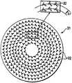
투과판(28)의 위쪽에는, 원판 형상의 평면 안테나 부재(31)가 마련되어 있다. 이 평면 안테나 부재(31)는 챔버(1)의 측벽 상단에 대하여 걸려서 고정되어 있다. 평면 안테나 부재(31)는, 예컨대 표면이 금 또는 은 도금된 구리판 또는 알 루미늄판으로 이루어지고, 마이크로파를 방사하는 다수의 슬롯 형상의 마이크로파 방사 구멍(32)이 소정의 패턴으로 관통하여 형성된 구성으로 되어 있다.The disk-shaped
마이크로파 방사 구멍(32)은, 예컨대 도 2에 도시하는 바와 같이, 긴 홈 형상을 이루고, 전형적으로는 인접하는 마이크로파 방사 구멍(32)끼리가 「T」자 형상으로 배치되고, 이들 복수의 마이크로파 방사 구멍(32)이 동심원 형상으로 배치되어 있다. 마이크로파 방사 구멍(32)의 길이나 배열 간격은 마이크로파의 파장(λg)에 따라 결정되며, 예컨대 마이크로파 방사 구멍(32)의 간격은 λg/4, λg/2 또는 λg가 되도록 배치된다. 또, 도 2에 있어서, 동심원 형상으로 형성된 인접하는 마이크로파 방사 구멍(32)끼리의 간격을 Δr로 나타내고 있다. 또한, 마이크로파 방사 구멍(32)은 원형 형상, 원호 형상 등의 다른 형상이더라도 좋다. 또한, 마이크로파 방사 구멍(32)의 배치 형태는 특별히 한정되지 않고, 동심원 형상 외에, 예컨대, 나선 형상, 방사 형상으로 배치할 수도 있다. 또한, 예컨대 피처리 기판이 LCD용의 직사각형 유리 기판인 경우에는, 마이크로파 방사 구멍(32)을 직선 형상으로 배치할 수도 있다.For example, as shown in FIG. 2, the
이 평면 안테나 부재(31)의 상면에는, 진공보다도 큰 유전율을 갖는 지파재(遲波材)(33)가 마련되어 있다. 이 지파재(33)는, 진공 중에서는 마이크로파의 파장이 길어지므로, 마이크로파의 파장을 짧게 하여 플라즈마를 조정하는 기능을 갖고 있다. 또, 평면 안테나 부재(31)와 투과판(28) 사이, 또한, 지파재(33)와 평면 안테나 부재(31) 사이는 각각 밀착시키더라도 이격시키더라도 무방하다.On the upper surface of this
챔버(1)의 상면에는, 이들 평면 안테나 부재(31) 및 지파재(33)를 덮도록, 예컨대 알루미늄이나 스테인리스강 등의 금속재로 이루어지는 쉴드 덮개(34)가 마련되어 있다. 챔버(1)의 상면과 쉴드 덮개(34)는 밀봉 부재(후술)에 의해 밀봉되어 있다. 쉴드 덮개(34)에는, 냉각수 유로(34a)가 형성되어 있고, 거기에 냉각수를 통류시킴으로써, 쉴드 덮개(34), 지파재(33), 평면 안테나 부재(31), 투과판(28)을 냉각하도록 되어 있다. 또, 쉴드 덮개(34)는 접지되어 있다.On the upper surface of the
도 3은 챔버(1)의 상부, 즉, 쉴드 덮개(34), 지파재(33), 평면 안테나 부재(31), 투과판(28) 및 상부 플레이트(27)의 접합 구조를 나타내는 주요부 단면도이다. 상부 플레이트(27)의 지지부(27a)에는, 투과판(28)이 O링 등의 밀봉 부재(71)를 거쳐서 기밀하게 지지되어 있다.3 is a cross-sectional view of an essential part showing the joining structure of the upper portion of the
또한, 고리 형상의 누름 부재(29)는 투과판(28)의 둘레부를 위로부터 O링 등의 밀봉 부재(73)를 거쳐서 밀어넣고, 또한, 상부 플레이트(27)에, 밀봉 부재(72)을 거쳐서, 볼트 등의 고정 부재(81)에 의해서 고정되어 있다. 금속제의 스파이럴 쉴드 링 등의 밀봉 부재(72)는 누름 부재(29)에 형성된 홈 내에 감입되어 있다. 이 밀봉 부재(72)에 의해서, 평면 안테나 부재(31)의 마이크로파 방사 구멍(32)으로부터 방사된 마이크로파가, 투과판(28)으로부터 상부 플레이트(27)와 누름 부재(29)와의 접합면을 거쳐서 외부로 누설되는 것이 방지되어 있다. 이 스파이럴 쉴드 링은, 예컨대 나선 형상의 스테인레스재에 의해 형성되어 있고, 마이크로파에 대하여 높은 차폐 성능을 가진다.In addition, the annular pressing
쉴드 덮개(34)의 아래에는, 평면 안테나 부재(31), 지파재(33)가 순서대로 배치되고, 이들은 내부 도체(41)(도 1 참조)에 의해 중앙부에서 고정되어 있다. 그리고, 평면 안테나 부재(31)의 외주부는, 아래측으로부터 볼트 등의 고정 부재(82)에 의해 쉴드 덮개(34)에 고정되어 있다. 또한, 평면 안테나 부재(31)는 투과판(28) 위에 배치된다. 투과판(28) 내의 외주에는, 고리 형상의 패임부(28c)가 형성되어 있고, 거기에 볼트 등의 고정 부재(82)가 감합된다.Under the
또한, 쉴드 덮개(34)는, 그 외주부의 직경 바깥 방향으로 돌기한 볼록부(34b)의 상면(34c)으로부터, 스파이럴 쉴드 링 등의 밀봉 부재(75)를 거쳐서, 단면에서 보아 L자형을 한 고리 형상의 누름 부재(35)에 의해서 밀어넣어져 있고, 누름 부재(35)는 볼트 등의 고정 부재(83)에 의해서 누름 부재(29)에 고정되어 있다. 이에 따라, 쉴드 덮개(34)와 지파재(33)가 고정된다. 누름 부재(35)와 누름 부재(29) 사이 및, 누름 부재(35)와 쉴드 덮개(34)와의 접합면에, 각각 스파이럴 쉴드 링 등의 밀봉 부재(74, 75)를 배치함으로써 마이크로파의 누설이 방지되어 있다.In addition, the
또, 쉴드 덮개(34)는 상하 두개의 부분으로 분리되어 구성되어 있으며, 양자의 접합에 의해서 냉각수 유로(34a)를 형성할 수 있도록, 볼트(84)에 의해서 고정되고, 접합부는 O링 등의 밀봉 부재(76)로 밀봉되어 있다.In addition, the
이러한 챔버(1) 상부의 접합 구조에 의해, 평면 안테나 부재(31)로부터의 마이크로파가 누출되는 것이 억제되어 있다. 이에 따라, 파워 손실을 억제하여, 마이크로파를 효율적이고 고출력으로 공급하는 것이 가능하게 되어, 높은 진공 상태로 소망하는 플라즈마 처리를 행할 수 있게 되어 있다.By the joining structure of the upper part of the
도 1을 참조하면, 쉴드 덮개(34)의 위쪽 벽의 중앙에는, 개구부(36)가 형성 되어 있으며, 이 개구부에는 도파관(37)이 접속되어 있다. 이 도파관(37)의 단부에는, 매칭 회로(38)를 거쳐서 마이크로파를 발생하는 마이크로파 발생 장치(39)가 접속되어 있다. 이에 따라, 마이크로파 발생 장치(39)에서 발생한, 예컨대 주파수 2.45㎓의 마이크로파가 도파관(37)을 거쳐서 상기 평면 안테나 부재(31)로 전파되게 되어 있다. 마이크로파의 주파수로서는, 8.35㎓, 1.98㎓ 등을 이용할 수도 있다.Referring to FIG. 1, an
도파관(37)은, 상기 쉴드 덮개(34)의 개구부(36)로부터 위쪽으로 연장되는 단면 원형 형상의 동축 도파관(37a)과, 이 동축 도파관(37a)의 상단부에 모드 변환기(40)를 거쳐서 접속된 수평 방향으로 연장되는 직사각형 도파관(37b)을 갖고 있다. 직사각형 도파관(37b)과 동축 도파관(37a) 사이의 모드 변환기(40)는 직사각형 도파관(37b) 내를 TE 모드로 전파하는 마이크로파를 TEM 모드로 변환하는 기능을 갖고 있다. 동축 도파관(37a)의 중심에는 내부 도체(41)가 연장되어 있으며, 내부 도체(41)는 그 하단부에서 평면 안테나 부재(31)의 중심에 접속 고정되어 있다. 이에 따라, 마이크로파는 동축 도파관(37a)의 내부 도체(41)를 거쳐서 평면 안테나 부재(31)로 방사 형상으로 효율적으로 균일하게 전파된다.The
플라즈마 산화 처리 장치(100)의 각 구성부는 CPU를 구비한 프로세스 제어기(50)에 접속되어 제어되는 구성으로 되어 있다. 프로세스 제어기(50)에는, 공정 관리자가 플라즈마 산화 처리 장치(100)를 관리하기 위해서 커맨드의 입력 조작 등을 행하는 키보드나, 플라즈마 산화 처리 장치(100)의 가동 상황을 가시화하여 표시하는 디스플레이 등으로 이루어지는 사용자 인터페이스(51)가 접속되어 있다.Each component of the
또한, 프로세스 제어기(50)에는, 플라즈마 산화 처리 장치(100)에서 실행되는 각종 처리를 프로세스 제어기(50)의 제어로 실현하기 위한 제어 프로그램(소프트웨어)나 처리 조건 데이터 등이 기록된 레시피가 저장된 기억부(52)가 접속되어 있다.The
그리고, 필요에 따라, 사용자 인터페이스(51)로부터의 지시 등에 의해 임의의 레시피를 기억부(52)로부터 호출하여 프로세스 제어기(50)에 실행시킴으로써, 프로세스 제어기(50)의 제어 하에서, 플라즈마 산화 처리 장치(100)에서의 소망하는 처리가 행하여진다. 또한, 상기 제어 프로그램이나 처리 조건 데이터 등의 레시피는 컴퓨터 판독 가능한 기억 매체, 예컨대 CD-ROM, 하드디스크, 플렉서블 디스크, 플래시 메모리 등에 저장된 상태의 것을 이용하거나, 또는, 다른 장치로부터, 예컨대 전용 회선을 거쳐서 수시로 전송시켜 온라인으로 이용하거나 하는 것도 가능하다.Then, if necessary, an arbitrary recipe is called from the
본 실시예의 플라즈마 산화 처리 장치(100)에서는, 탑재대(2) 상에 탑재된 웨이퍼 W와 이것에 대향 배치된 투과판(28)과의 간격(갭 G)이, 예컨대 20㎜~100㎜, 바람직하게는 20~80㎜로 되도록 설정하고 있다. 평면 안테나 부재(31)로부터 도입되는 마이크로파에 의해 여기된 처리 가스의 플라즈마는, 플라즈마 처리 공간을 투과판(28)의 바로 근방 위치로부터 탑재대(2)에 탑재된 웨이퍼 W로 향해서 강하해 가지만, 도 4에 도시하는 바와 같이, 플라즈마의 전자 온도는 투과판(28)과의 거리가 가까운 영역에서는 극단적으로 높고, 투과판(28)으로부터 약 20㎜ 이상 떨어지면 1.2[eV] 이하로 저하하여 안정화된다. 따라서, 갭 G가 20㎜ 미만인 경우에는, 높은 전자 온도의 플라즈마(예컨대 전자 온도 1.2[eV]초의 플라즈마)가 직접 웨이퍼 W에 작용함으로써, 웨이퍼 W에 플라즈마 손상이 발생하는 경우가 있다.In the plasma
한편, 갭 G가 80㎜를 초과하면, 소한 부분과 밀한 부분에서의 산화막 두께의 차가 발생하기 쉬워지고, 갭 G가 100㎜를 초과하면, 웨이퍼 W 상에 형성된 소밀의 임의의 패턴에 있어서, 소한 부분과 밀한 부분에서의 산화막 두께의 차를 허용할 수 있기가 어려워진다. 또한, 웨이퍼 W 상에 형성된 홈의 어스펙트비(홈의 폭에 대한 깊이의 비)에 상위가 있는 패턴에 있어서도, 낮은 어스펙트비의 부분과 높은 어스펙트비의 부분에서 차가 발생한다. 소밀차가 발생하면, 밀한 부분 또는 높은 어스펙트비의 부분에서는, 소한 부분 또는 낮은 어스펙트비의 부분에 비해서 막 두께가 얇아져, 반도체 장치의 성능에 영향을 미쳐, 그 신뢰성을 저하시키는 요인으로 된다.On the other hand, when gap G exceeds 80 mm, the difference of the oxide film thickness in a small part and a dense part tends to generate | occur | produce, and when gap G exceeds 100 mm, in the arbitrary pattern of the roughness formed on the wafer W, It becomes difficult to tolerate the difference in oxide film thickness between the portion and the dense portion. Moreover, also in the pattern which differs in the aspect ratio (ratio of the depth to the groove width) of the groove | channel formed on the wafer W, the difference generate | occur | produces in the part of low aspect ratio and the part of high aspect ratio. When a small difference occurs, in a dense part or a part of high aspect ratio, compared with a little part or a part of low aspect ratio, a film thickness becomes thin and it affects the performance of a semiconductor device, and becomes a factor which reduces the reliability.
이러한 소밀차가 발생하는 원인으로서, 플라즈마 중의 산소 이온, 산소 래디컬 등의 산화종이나, 산화를 어시스트하는 수소 이온, 수소 래디컬 등이 패턴 조밀부나 높은 어스펙트비 홈의 바닥 부근에 충분히 공급되지 않는 것이 생각된다. 특히 산화 반응의 어시스트종인 수소 이온이나 수소 래디컬은 소실되기 쉽기 때문에, 갭 G가 큰 경우에는 패턴 조밀부나 높은 어스펙트비 홈의 바닥 부근에 도달하기 전에 소실되어, 산화 반응에 기여할 수 없어지게 된다.As a cause of such a small difference, it is thought that oxidized species such as oxygen ions and oxygen radicals in the plasma, hydrogen ions assisting oxidation, hydrogen radicals, and the like are not sufficiently supplied near the bottom of the pattern dense portion or the high aspect ratio groove. do. In particular, since hydrogen ions and hydrogen radicals, which are assist species of the oxidation reaction, are easily lost, when the gap G is large, they are lost before reaching near the bottom of the pattern dense portion or the high aspect ratio groove, and cannot contribute to the oxidation reaction.
또한, 갭 G가 커짐에 따라, 서서히 산화 레이트도 저하해가기 때문에, 이 관점으로부터도 갭 G를 지나치게 확대하는 것은 바람직하지 못하다.In addition, since the oxidation rate also gradually decreases as the gap G increases, it is not preferable to enlarge the gap G too much from this viewpoint.
이상으로부터, 본 실시예에서는 갭 G를, 종래의 130~150㎜보다도 좁은 100㎜ 이하, 바람직하게는 80㎜ 이하로 설정함으로써, 상기 산화종이나 어시스트종의 공 급을 촉구하여, 웨이퍼 W 상의 패턴의 소밀이나 어스펙트비에 관계없이, 산화막 두께의 균일화를 도모하고 있다. 또, 본 실시예에 있어서는, 탑재대(2)에 서셉터 커버(2a)를 마련했기 때문에, 갭 G를 종래의 130~150㎜에 비하여 좁은 20~100㎜, 또는 20~80㎜로 설정하더라도 이물질의 발생을 방지할 수 있다.In view of the above, in the present embodiment, the gap G is set to 100 mm or less, preferably 80 mm or less, which is narrower than the conventional 130 to 150 mm, thereby prompting the supply of the oxidized species and the assist species, thereby providing a pattern on the wafer W. Irrespective of the density and the aspect ratio, the thickness of the oxide film is made uniform. In the present embodiment, since the
또한, 갭 G를 20~100㎜, 바람직하게는 20~80㎜로 설정하는 것에 부가하여, 처리 압력을 1.33Pa 이하로 하는 것이 바람직하며, 1.33Pa~66.66Pa로 하는 것이 보다 바람직하다. 이것에 의해서, 실용상 충분한 산화 레이트를 얻는 것이 가능하게 된다.In addition to setting the gap G to 20 to 100 mm, preferably 20 to 80 mm, the processing pressure is preferably 1.33 Pa or less, more preferably 1.33 Pa to 66.66 Pa. This makes it possible to obtain a practically sufficient oxidation rate.
또한, 갭 G를 보다 바람직한 20~80mm로 설정하는 것의 효과는 처리 압력이 1.33~66.66Pa 정도의 저압측에서 특히 현저히 발현된다. 그 이유는, 처리 압력이 상기 범위보다도 고압측, 예컨대 400Pa에서는, 플라즈마 중의 산화종이나 어시스트종의 절대수가 커지기 때문에, 실리콘의 산화 반응이 반응율속의 상태로 되어, 소밀차 자체가 발생하기 어렵게 되는 데 반하여, 처리 압력이 1.33~66.66Pa와 저압측에서는, 실리콘의 산화 반응이 공급율속의 상태로 되기 때문에, 갭 G를 20~80㎜로 하여, 패턴이 조밀하게 형성된 부분이나, 높은 어스펙트비의 홈의 속(바닥부)에까지 상기 산화종이나 어시스트종의 공급을 증가시키는 것에 의한, 소밀차 개선 효과가 커지기 때문이다.Moreover, the effect of setting gap G to 20 to 80 mm which is more preferable is especially remarkably expressed on the low pressure side about 1.33-66.66 Pa of processing pressures. The reason is that, on the high pressure side, for example, 400 Pa, the absolute number of oxidized species and assisted species in the plasma becomes larger than the above range, so that the oxidation reaction of silicon is brought into a reaction rate state, so that it is difficult to produce a compactness difference itself. On the other hand, at the processing pressure of 1.33 to 66.66 Pa and the low pressure side, since the oxidation reaction of silicon is in a state of supply rate, the gap G is set to 20 to 80 mm so that the pattern is densely formed or the groove having a high aspect ratio. This is because the effect of improving the compactness difference is increased by increasing the supply of the oxidized species and the assist species to the inside (bottom).
이와 같이 구성된 RLSA 방식의 플라즈마 산화 처리 장치(100)에 있어서는, 웨이퍼 W 표면의 실리콘(다결정 실리콘 또는 단결정 실리콘)을 산화하여 실리콘 산화막을 형성하는 처리를 행할 수 있다. 이하, 그 수순에 관하여 설명한다.In the RLSA type
우선, 게이트 밸브(26)를 열어서 반입출구(25)로부터 실리콘 표면을 갖는 웨이퍼 W를 챔버(1) 내로 반입해 탑재대(2) 상에 탑재한다. 그리고, 가스 공급계(16a)의 Ar 가스 공급원(17a), O2 가스 공급원(18a) 및 H2 가스 공급원(19a)으로부터, Ar 가스, O2 가스 및 H2 가스를 소정의 유량으로 가스 도입 부재(15)를 거쳐서 챔버(1) 내에 도입한다.First, the
구체적으로는, 예컨대 Ar 등의 희가스 유량을 500~2000mL/min(sccm), O2 가스 유량을 5~200mL/min(sccm), 필요에 따라 H2 가스 유량을 5~200mL/min(sccm)으로 설정하고, 챔버 내를 1.33Pa~66.66Pa(10mTorr~500mTorr)의 처리 압력으로 조정하며, 웨이퍼 W의 온도를 200~800℃, 바람직하게는 250~500℃ 정도로 가열한다.Specifically, for example, a rare gas flow rate such as Ar is 500 to 2000 mL / min (sccm), the O2 gas flow rate is 5 to 200 mL / min (sccm), and if necessary, the H2 gas flow rate is 5 to 200 mL / min (sccm). The inside of the chamber is adjusted to a processing pressure of 1.33 Pa to 66.66 Pa (10 mTorr to 500 mTorr), and the temperature of the wafer W is heated to about 200 to 800 ° C, preferably about 250 to 500 ° C.
다음에, 마이크로파 발생 장치(39)로부터의 마이크로파를, 매칭 회로(38)를 지나서 도파관(37)으로 유도하여, 직사각형 도파관(37b), 모드 변환기(40), 및 동축 도파관(37a)을 순차적으로 통과시켜 내부 도체(41)를 거쳐서 평면 안테나 부재(31)에 공급해서, 평면 안테나 부재(31)의 마이크로파 방사 구멍(32)으로부터 투과판(28)을 거쳐서 챔버(1) 내에서의 웨이퍼 W의 위쪽 공간에 방사시킨다. 마이크로파는, 직사각형 도파관(37b) 내에서는 TE 모드로 전파해서, 이 TE 모드의 마이크로파는 모드 변환기(40)에서 TEM 모드로 변환되어, 동축 도파관(37a) 내를 평면 안테나 부재(31)로 향해 전파되어 간다. 이 때의 마이크로파 파워는, 예컨대 1000~4000W로 할 수 있다.Next, the microwaves from the
평면 안테나 부재(31)로부터 투과판(28)을 지나서 챔버(1)에 방사된 마이크 로파에 의해 챔버(1) 내에서 전자계가 형성되어, Ar 가스, O2 가스 및 H2 가스가 플라즈마화된다. 이 산소 함유 플라즈마는 마이크로파가 평면 안테나 부재(31)의 다수의 마이크로파 방사 구멍(32)으로부터 방사됨으로써, 약 1×10¹⁰~5×10¹²/㎝3의 고플라즈마 밀도이고, 또한 웨이퍼 W 근방에서는, 약 1.2eV 이하의 낮은 전자 온도 플라즈마로 된다. 이렇게 하여 형성되는 마이크로파 여기 플라즈마는 이온 등에 의한 플라즈마 손상이 적은 것이다. 그리고, 플라즈마 중의 활성종, 주로 O 래디컬의 작용에 의해서, 실리콘 중에 산소가 도입되어, 실리콘 표면에 균일하게 SiO2막이 형성된다.Electromagnetic fields are formed in the
본 실시예에서는, 플라즈마 산화 처리 장치(100)를 이용하여, 실리콘(다결정 실리콘 또는 단결정 실리콘)을 플라즈마에 의해 산화 처리해서 실리콘 산화막의 형성을 행하는 플라즈마 처리에 있어서, 갭 G를 20~100㎜, 바람직하게는 20~80㎜로 설정함으로써, 웨이퍼 W 상에 존재하는 라인&스페이스의 패턴이나 어스펙트비가 다른 트렌치 패턴 등에 있어서, 소밀차를 발생시키지 않고, 실리콘을 산화할 수 있다.In the present embodiment, in the plasma processing in which silicon (polycrystalline silicon or single crystal silicon) is oxidized by plasma to form a silicon oxide film by using the plasma
이상과 같이 하여, 단결정 실리콘이나 다결정 실리콘의 표면에 양질의 실리콘 산화막을 형성할 수 있다. 따라서, 본 실시예의 플라즈마 산화 처리 방법은, 각종 반도체 장치의 제조 과정에서, 여러 가지의 용도의 실리콘 산화막을 형성하는 경우에 이용 가능하다. 예컨대, 플라즈마 산화 처리 장치(100)는, 트랜지스터의 게이트 전극의 폴리실리콘층의 측벽의 산화 처리나, STI(Shallow Trench Isolation)에 의한 트렌치 내부의 산화막 형성, 캐패시터 하부 전극의 폴리실리콘 산화, 플래쉬 메모리 소자의 측벽 산화 등에 적합하게 이용 가능한 것이다.As described above, a high quality silicon oxide film can be formed on the surface of single crystal silicon or polycrystalline silicon. Therefore, the plasma oxidation treatment method of the present embodiment can be used when forming silicon oxide films for various uses in the manufacturing process of various semiconductor devices. For example, the plasma
게이트 전극으로서는, 예컨대 실리콘 웨이퍼 등의 Si 기판 상에 게이트 절연막을 거쳐서 폴리실리콘층을 형성한 것이나, Si 기판 상에 게이트 절연막을 거쳐서 폴리실리콘층을 형성하고, 또한 그 위에 텅스텐 실리사이드(WSi) 등의 금속 실리사이드층을 형성한 폴리사이드 구조나, Si 기판 상에 게이트 절연막을 거쳐서 폴리실리콘층을 형성하고, 또한 그 상층에 텅스텐 나이트라이드(WN) 등의 배리어층 및 텅스텐(W) 등의 금속층을 순차적으로 형성한, 고속의 디바이스에 이용되는 저항이 낮은 폴리메탈 게이트 구조 등의 게이트를 들 수 있다.Examples of the gate electrode include a polysilicon layer formed on a Si substrate such as a silicon wafer via a gate insulating film, a polysilicon layer formed on a Si substrate via a gate insulating film, and a tungsten silicide (WSi) or the like thereon. Polysilicon structure in which a metal silicide layer is formed or a polysilicon layer is formed on a Si substrate via a gate insulating film, and a barrier layer such as tungsten nitride (WN) and a metal layer such as tungsten (W) are sequentially formed thereon. And a gate such as a low-resistance polymetal gate structure used for a high-speed device.
또한, 텅스텐(W) 등의 금속을 포함하는 게이트 전극의 경우에, 플라즈마 산화 처리 장치(100)를 이용하여, 고밀도 플라즈마에 의해 H2를 포함하는 가스 배합으로 폴리실리콘의 산화 처리를 행하는 것에 의해, 텅스텐(W)의 산화에 의한 WOx(WO3, WO2, 또는 WO)의 승화를 적극 억제하여 매우 고밀도의 처리를 행할 수 있다.In addition, in the case of a gate electrode containing a metal such as tungsten (W), by using the
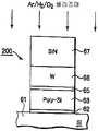
다음에, 본 발명 방법을 이용한 반도체 장치의 제조 공정을, DRAM 등의 반도체 장치의 MOS 트랜지스터를 구성하는 게이트 전극을 예로 들어 설명한다. 도 5~도 7은 게이트 전극(200)에 선택적으로 산화막(68)이 형성되는 모양을 모식적으로 나타내는 것이다. 도 5는 에칭 후의 게이트 전극(200)을 나타내고 있다.Next, a manufacturing process of a semiconductor device using the method of the present invention will be described taking a gate electrode constituting a MOS transistor of a semiconductor device such as a DRAM as an example. 5 to 7 schematically show how the
게이트 전극(200)의 제작 순서로서는, 우선, Si 기판(61)에, 불순물이 도핑되어 P+ 또는 N로 된 웰 영역(확산 영역 ; 도시하지 않음)이 형성되고, 이어서 열 산화 처리 등에 의해, 게이트 절연막(62)(SiO2)이 형성된다. 게이트 절연막(62) 상에는 CVD에 의해 폴리실리콘을 성막하고, 폴리실리콘층(63)을 형성하여, 그 위에 또 게이트 전극(200)을 고속화하기 위해 비(比)저항을 낮출 목적으로, 고융점 전극 재료인 텅스텐에 의해 텅스텐층(66)을 형성한다. 텅스텐층(66)의 형성에는, 예컨대 CVD법이나 스퍼터법을 이용할 수 있다. 텅스텐층(66) 대신에 텅스텐 실리사이드(WSi)를 이용할 수도 있다. 또, 텅스텐층(66)을 형성하기 전에, 그 계면에서 W와 Si의 상호 확산에 의해 실리사이드화가 발생하여, 높은 저항의 WSi가 확산되는 것을 방지하기 위해서, 미리 폴리실리콘층(63) 위에 매우 얇은 확산 배리어층(65)으로서, 예컨대 질화막(SiN막)을 형성해 놓는다. 이 예에서는, 텅스텐 나이트라이드를 배리어층(65)으로 이용하고 있다. 또, 이 질화막(SiN)은 폴리실리콘을 NH3, N2, 또는 N2와 H2의 혼합 가스 등을 이용하여 질화시키는 것에 의해 형성하더라도 좋다. 또한, 이 경우, 후술하는 실시예의 플라즈마 질화 처리 장치(101)(도 10)를 이용하여 플라즈마 질화 처리를 행하더라도 좋다.As the fabrication procedure of the
텅스텐층(66) 위에는, 질화 실리콘 등의 하드 마스크층(67)을 형성하고, 또한 포토레지스트막(도시하지 않음)을 형성해 놓는다.On the
그 후, 포토리소그래피에 의해 포토레지스트막을 마스크로 하여 하드 마스크층(67)을 에칭하고, 또한 포토레지스트막+하드 마스크층(67) 또는 하드 마스크층(67)을 마스크로 하여 텅스텐층(66), 배리어층(65), 폴리실리콘층(63)을 순차적으로 에칭해서 게이트 전극(200)을 형성한다. 일련의 에칭 처리에 의해, 게이트 전극(200)의 측면에는 폴리실리콘층(63) 및 텅스텐층(66)의 측벽이 노출되고, 또한 게이트 절연막(62)도 에칭에 의해 제거되어 Si 기판(61) 표면이 노출된 상태로 되어 있다.Thereafter, the
이와 같이 형성된 게이트 전극(200)에 대하여, 도 6에 도시하는 바와 같이, 플라즈마 산화 처리 장치(100)에 의해, 수소 가스와 산소 가스를 소정의 유량비로 되도록 제어하면서 플라즈마 산화 처리를 행한다. 여기서, 텅스텐의 산화를 억제하면서 폴리실리콘만을 선택적으로 산화하는 관점에서, H2와 O2의 유량비(H2/O2)는 1 이상으로 하는 것이 좋고, 2 이상, 예컨대 2~8로 하는 것이 바람직하다.As shown in FIG. 6, the plasma
플라즈마 산화 처리 조건으로서는, 산화막의 웨이퍼 W의 면상에 있어서의 균일성, 특히 게이트 패턴의 소밀에 의한 폴리실리콘층(63) 측벽의 산화막 두께의 차(소밀차)를 해소하기 위해서, 갭 G를 20~100mm, 바람직하게는 20~80㎜로 설정한다.As the plasma oxidation treatment conditions, the gap G is set to 20 to eliminate the difference (thickness difference) of the oxide film thickness between the sidewalls of the
이러한 조건에서 플라즈마 산화 처리를 행하는 것에 의해, 산화막(68)이 폴리실리콘층(63)의 표면에 선택적으로, 또한 게이트 패턴의 소밀에 관계없이 균일하게 형성된다. 텅스텐층(66) 및 배리어층(65)의 측벽에는 산화막이 형성되지 않고, 도 7에 나타내는 바와 같은 게이트 전극(210)으로 된다. 또, Si 기판 및 SiN 표면에도, 약간의 산화막이 형성된다. 텅스텐층(66) 대신에, 다른 고융점 재료, 예컨대, 몰리브덴, 탄탈, 티탄, 그들의 실리사이드, 나이트라이드, 합금 등을 성막한 게이트 전극에 관해서도 마찬가지로 처리할 수 있다.By performing the plasma oxidation treatment under such conditions, the
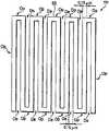
다음에, 본 발명의 기초로 된 실험 데이터에 대하여 설명을 한다. 도 1의 플라즈마 산화 처리 장치(100)를 이용하여, 도 8의 평면도에 나타내는 라인&스페이스의 테스트 패턴 TP을 작성하였다. 폴리실리콘층(63)(라인)의 폭은 0.15㎛, 라인끼리의 간격(스페이스)은 0.15㎛로 하였다. 이 테스트 패턴 TP에 대하여, 도 1에 나타내는 플라즈마 산화 처리 장치(100)를 이용해서, 갭 G를 변경하여 폴리실리콘층(63)의 측벽 산화를 실시하였다. 갭 G는 79㎜, 105㎜, 134㎜의 3가지로 하였다.Next, experimental data based on the present invention will be described. The test pattern TP of the line & space shown in the top view of FIG. 8 was created using the plasma
플라즈마 산화 처리에 있어서의 처리 가스의 유량은 Ar/O2/H2=1000/10/10mL/min(sccm), 처리 온도(기판 처리 온도)는 250℃이고, 플라즈마로의 공급 파워는 3㎾, 처리 시간은 베어실리콘 기판 표면에 실리콘 산화막을 6㎚의 두께로 형성할 수 있도록 설정하였다. 산화 처리 후의 폴리실리콘층(63)의 측벽의 산화막의 막 두께를, 테스트 패턴 TP의 오픈 부위 Op와 밀집 부위 De로 나누어 각각 측정하였다.The flow rate of the processing gas in the plasma oxidation treatment was Ar / O2 / H2 = 1000/10/10 mL / min (sccm), the treatment temperature (substrate treatment temperature) was 250 ° C., and the supply power to the plasma was 3 kW. The processing time was set so that a silicon oxide film could be formed in the thickness of 6 nm on the bare silicon substrate surface. The film thickness of the oxide film on the sidewall of the
도 9에, 각 갭 G로 산화 처리를 행한 후의 폴리실리콘층(63)의 측벽의 산화막의 막 두께와, 테스트 패턴 TP의 오픈 부위 Op와 밀집 부위 De와의 해당 산화막의 막 두께의 비율(소밀비)을 나타낸다. 또, 도 9에 있어서의 세로축의 소밀비(%)는 밀집 부위 De의 산화막 두께를 오픈 부위 Op의 산화막 두께에 대한 백분율로 나타낸 것으로, 그 값이 100에 가까울수록, 소밀차가 적고, 균일한 산화막이 형성된 것을 나타내고 있다.9 shows the ratio of the film thickness of the oxide film on the sidewall of the
도 9로부터, 갭 G가 작아짐에 따라 소밀비가 상승하는 경향이 있어, 갭 G가 79㎜인 경우는, 소밀비가 100%에 근접하여 적어지고, 밀집 부위 De와 오픈 부위 Op에서 대략 동등한 막 두께로 측벽 산화막이 얻어지고 있는 것을 확인하였다. 이로부터, 갭 G를 100㎜ 이하, 특히 80㎜ 이하로 함으로써, 소밀차를 작게 하여 균일한 막 두께로 산화막(68)을 형성할 수 있는 것이 확인되었다. 이에 반하여, 갭 G를 105㎜나 134㎜로 한 경우에는, 소밀비의 값이 저하되어 있어, 소밀차가 확대되고 있는 것이 나타났다. 또한, 갭 G를 79㎜ 또는 105㎜로 한 경우는, 갭 G를 134㎜로 한 경우에 비해서, 산화 레이트도 큰 것을 알 수 있었다. 이상의 결과로부터, 갭 G를 100㎜ 이하, 특히 80㎜로 설정하여 플라즈마 산화 처리를 행하는 것에 의해, 소밀차를 개선할 수 있고, 또한, 실용상 충분한 산화 레이트를 얻을 수 있는 것이 확인되었다.As shown in FIG. 9, the roughness ratio tends to increase as the gap G decreases. When the gap G is 79 mm, the roughness ratio decreases to 100%, and the film thickness is approximately equal in the dense site De and the open site Op. It was confirmed that the sidewall oxide film was obtained. From this, it was confirmed that by setting the gap G to 100 mm or less, particularly 80 mm or less, the
다음에, 다른 실시예에 대해 설명한다.Next, another Example is described.
도 10은 본 발명의 다른 실시예에 따른 플라즈마 질화 처리 방법에 적합하게 이용 가능한 플라즈마 질화 처리 장치(101)의 일례를 모식적으로 나타내는 단면도이다. 이 플라즈마 질화 처리 장치(101)는, 처리 가스의 공급계가 다른 점 이외에는 도 1의 플라즈마 산화 처리 장치(100)와 동일한 구성이기 때문에, 다른 점에 대해서만 설명을 하고, 동일한 구성에 대해서는 동일한 부호를 부여하고 설명을 생략한다.10 is a cross-sectional view schematically showing an example of the plasma nitridation processing apparatus 101 that can be suitably used for the plasma nitridation processing method according to another embodiment of the present invention. Since the plasma nitridation processing apparatus 101 has the same configuration as the plasma
플라즈마 질화 처리 장치(101)에 있어서, 가스 공급계(16b)는, 예컨대 Ar 가스 공급원(17b) 및 N2 가스 공급원(18b)을 갖고 있으며, Ar 가스 및 N2 가스가 각각 가스 라인(20)을 거쳐서 가스 도입 부재(15)에 도달하여, 가스 도입 부재(15)로부터 챔버(1) 내로 도입된다. 가스 라인(20)의 각각에는, 매스플로우 제어기(21) 및 그 전후의 개폐 밸브(22)가 마련되어 있다. 또, 플라즈마 질화 처리 장치(101)에 있어서는, Ar 가스 대신에, 예컨대 Kr 가스, Xe 가스, He 가스 등의 희가스를 이용할 수 있다. 또한, N2 가스 대신에, 예컨대 NH3 가스, N2와 H2의 혼합 가스, 히드라진 등을 이용할 수 있다.In the plasma nitridation apparatus 101, the
본 실시예의 플라즈마 질화 처리 장치(101)에서는, 탑재대(2)에 탑재되어 웨이퍼 W와 이들에 대향 배치된 투과판(28)과의 간격(갭 G)을, 전술한 실시예와 동일한 이유에 의해, 예컨대 20~100㎜, 바람직하게는 20~80㎜로 설정하고 있다. 갭 G가 20㎜ 미만인 경우에는, 높은 전자 온도의 플라즈마, 예컨대 전자 온도 1.2[eV]초의 플라즈마가 직접 웨이퍼 W에 작용하기 때문에, 웨이퍼 W에 플라즈마 손상이 발생하는 경우가 있다. 또한, 갭 G가 100㎜을 초과하는 경우에는, 패턴의 소밀에 의해서 질화막 두께에 차(소밀차)가 발생하기 쉬워짐에 부가하여, 갭 G가 커짐에 따라, 질화 레이트도 저하되기 때문에 바람직하지 못하다. 갭 G가 100㎜ 이하이면, 소밀비가 80% 정도 이상으로 하고, 또한, 질화 레이트를 낮추지 않고 질화하는 것이 가능하다.In the plasma nitriding apparatus 101 of the present embodiment, the gap (gap G) between the wafer W and the
이와 같이 구성된 RLSA 방식의 플라즈마 질화 처리 장치(101)에 있어서는, 웨이퍼 W 표면의 실리콘(다결정 실리콘 또는 단결정 실리콘)을 질화하여 실리콘 질화막을 형성하는 처리를 행할 수 있다. 이하, 그 수순에 관하여 설명한다.In the RLSA type plasma nitriding apparatus 101 configured as described above, a process of nitriding silicon (polycrystalline silicon or single crystal silicon) on the wafer W surface to form a silicon nitride film can be performed. Hereinafter, the procedure will be described.
우선, 게이트 밸브(26)를 개방하여 반입출구(25)로부터 실리콘 표면을 갖는 웨이퍼 W를 챔버(1) 내에 반입하고, 탑재대(2) 상에 탑재한다. 그리고, 가스 공급계(16b)의 Ar 가스 공급원(17b) 및 N2 가스 공급원(18b)으로부터 Ar 가스 및 N2 가스를 소정의 유량으로 가스 도입 부재(15)를 거쳐서 챔버(1) 내에 도입한다.First, the
구체적으로는, 예컨대 Ar 등의 희가스 유량을 500~2000mL/min(sccm), N2 가스 유량을 5~200mL/min(sccm)으로 설정하고, 챔버 내를 1.33Pa~133.3Pa(10mTorr~1000mTorr)의 처리 압력으로 조정하여, 웨이퍼 W의 온도를 200~800℃, 바람직하게는 250~500℃ 정도로 가열한다.Specifically, for example, a rare gas flow rate such as Ar is set to 500 to 2000 mL / min (sccm), and the N2 gas flow rate is set to 5 to 200 mL / min (sccm), and the inside of the chamber is 1.33 Pa to 133.3 Pa (10 mTorr to 1000 mTorr). It adjusts to the process pressure of and heats the temperature of the wafer W about 200-800 degreeC, Preferably it is about 250-500 degreeC.
다음에, 마이크로파 발생 장치(39)로부터의 마이크로파를, 매칭 회로(38)를 지나서 도파관(37)으로 유도하여, 직사각형 도파관(37b), 모드 변환기(40), 및 동축 도파관(37a)을 순차적으로 통과시켜 내부 도체(41)를 거쳐서 평면 안테나 부재(31)에 공급하여, 평면 안테나 부재(31)의 마이크로파 방사 구멍(32)으로부터 투과판(28)을 거쳐서 챔버(1) 내에서의 웨이퍼 W의 위쪽 공간에 방사시킨다. 마이크로파는, 직사각형 도파관(37b) 내에서는 TE 모드로 전파하고, 이 TE 모드의 마이크로파는 모드 변환기(40)에서 TEM 모드로 변환되어, 동축 도파관(37a) 내를 평면 안테나 부재(31)로 향해 전파되어 간다. 이 때의 마이크로파 파워는, 예컨대 1000~4000W로 할 수 있다.Next, the microwaves from the
평면 안테나 부재(31)로부터 투과판(28)을 지나서 챔버(1)로 방사된 마이크로파에 의해 챔버(1) 내에서 전자계가 형성되어, Ar 가스 및 N2 가스가 플라즈마화 된다. 이 질소 함유 플라즈마는, 마이크로파가 평면 안테나 부재(31)의 다수의 마이크로파 방사 구멍(32)으로부터 방사되는 것에 의해, 약 1×10¹⁰~5×10¹²/㎤의 높은 플라즈마 밀도이고, 또한 웨이퍼 W 근방에서는 약 1.2eV 이하의 낮은 전자 온도 플라즈마로 된다. 이렇게 하여 형성되는 마이크로파 여기 플라즈마는 이온 등에 의한 플라즈마 손상이 적은 것이다. 그리고, 플라즈마 중의 활성종, 주로 N 래디컬의 작용에 의해서, 실리콘 중에 질소가 도입되어, 실리콘 표면에 균일하게 실리콘 질화막(Si3N4막)이 형성된다.Electromagnetic fields are formed in the
본 실시예에서는, 플라즈마 질화 처리 장치(101)를 이용하여, 실리콘(다결정 실리콘 또는 단결정 실리콘)을 플라즈마에 의해 질화 처리해서 실리콘 질화막의 형성을 행하는 플라즈마 처리에 있어서, 갭 G를 20~100㎜, 바람직하게는 20~80㎜로 설정함으로써, 상기 플라즈마 산화 처리의 경우와 마찬가지로, 웨이퍼 W 상에 존재하는 라인&스페이스의 패턴이나 어스펙트비가 다른 트렌치 패턴 등에서, 소밀차를 발생시키지 않고, 실리콘 질화막을 형성할 수 있다.In the present embodiment, in the plasma processing in which silicon (polycrystalline silicon or single crystal silicon) is nitrided by plasma to form a silicon nitride film by using the plasma nitride processing apparatus 101, the gap G is 20 to 100 mm, Preferably, the silicon nitride film is formed without causing a small difference in the pattern of the line and space existing on the wafer W and the trench pattern having different aspect ratios, as in the case of the plasma oxidation treatment, by setting it to 20 to 80 mm. Can be formed.
이상과 같이 하여, 단결정 실리콘이나 다결정 실리콘의 표면에 양질의 실리콘 질화막을 형성할 수 있다. 따라서, 본 실시예의 플라즈마 질화 처리 방법은, 각종 반도체 장치의 제조 과정에서, 예컨대, 트랜지스터의 게이트 전극의 폴리실리콘층의 측벽 질화막의 형성이나 게이트 사이드 월 스페이서(TEOS) 등의 측벽 질화막의 형성, STI에서의 트렌치 내벽의 질화막의 형성 등의 목적으로 실리콘 질화 처리를 행하는 경우에 이용 가능하다.As described above, a high quality silicon nitride film can be formed on the surface of single crystal silicon or polycrystalline silicon. Therefore, the plasma nitriding treatment method of the present embodiment is, for example, in the production of various semiconductor devices, for example, formation of sidewall nitride films of polysilicon layers of gate electrodes of transistors, formation of sidewall nitride films such as gate sidewall spacers (TEOS), and STI. It can be used when the silicon nitride treatment is carried out for the purpose of forming a nitride film of the trench inner wall in.
또, 본 발명은 상기 실시예에 한정되지 않고, 다양한 변형이 가능히다.In addition, this invention is not limited to the said Example, A various deformation | transformation is possible.
예컨대, 상기 실시예에서는 피처리체로서 반도체 웨이퍼, 특히 실리콘 웨이퍼에 대하여, 산화 처리나 질화 처리를 행하는 예를 들었지만, 반도체 웨이퍼로서는 실리콘 웨이퍼에 한정되지 않고 화합물 반도체 웨이퍼를 이용할 수 있고, 또한, 반도체 웨이퍼에 한정되지 않고, 예컨대 피처리체가 액정 표시 디스플레이(LED)로 대표되는 플랫 패널 디스플레이(FPD)용의 유리 기판인 경우에도 응용 가능하다.For example, in the above embodiment, an example of performing oxidation treatment or nitriding treatment on a semiconductor wafer, in particular, a silicon wafer, as a target object is not limited to a silicon wafer, but a compound semiconductor wafer can be used as the semiconductor wafer. It is not limited to this, For example, it is applicable also when the to-be-processed object is a glass substrate for flat panel displays (FPD) represented by liquid crystal display display (LED).
이상 설명한 바와 같이, 본 발명에 의하면, 플라즈마 처리에 의해서 형성되는 산화막이나 질화막에 있어서, 막 두께의 소밀차가 발생하기 어려운 플라즈마 처리 장치 및 플라즈마 처리 방법을 얻을 수 있다.As described above, according to the present invention, it is possible to obtain a plasma processing apparatus and a plasma processing method in which a small difference in film thickness hardly occurs in an oxide film or a nitride film formed by plasma processing.
Claims (25)
Translated fromKoreanApplications Claiming Priority (2)
| Application Number | Priority Date | Filing Date | Title |
|---|---|---|---|
| JPJP-P-2006-00085380 | 2006-03-27 | ||
| JP2006085380 | 2006-03-27 |
Related Child Applications (2)
| Application Number | Title | Priority Date | Filing Date |
|---|---|---|---|
| KR1020090061004ADivisionKR100935488B1 (en) | 2006-03-27 | 2009-07-06 | Plasma processing equipment |
| KR1020100031789ADivisionKR101020334B1 (en) | 2006-03-27 | 2010-04-07 | Microwave plasma processing apparatus |
Publications (2)
| Publication Number | Publication Date |
|---|---|
| KR20070096955A KR20070096955A (en) | 2007-10-02 |
| KR100980529B1true KR100980529B1 (en) | 2010-09-06 |
Family
ID=38532094
Family Applications (4)
| Application Number | Title | Priority Date | Filing Date |
|---|---|---|---|
| KR1020070029327AExpired - Fee RelatedKR100980529B1 (en) | 2006-03-27 | 2007-03-26 | Plasma processing equipment |
| KR1020090061004AExpired - Fee RelatedKR100935488B1 (en) | 2006-03-27 | 2009-07-06 | Plasma processing equipment |
| KR1020100031789AExpired - Fee RelatedKR101020334B1 (en) | 2006-03-27 | 2010-04-07 | Microwave plasma processing apparatus |
| KR1020100110505AExpired - Fee RelatedKR101097574B1 (en) | 2006-03-27 | 2010-11-08 | microwave plasma processing apparatus |
Family Applications After (3)
| Application Number | Title | Priority Date | Filing Date |
|---|---|---|---|
| KR1020090061004AExpired - Fee RelatedKR100935488B1 (en) | 2006-03-27 | 2009-07-06 | Plasma processing equipment |
| KR1020100031789AExpired - Fee RelatedKR101020334B1 (en) | 2006-03-27 | 2010-04-07 | Microwave plasma processing apparatus |
| KR1020100110505AExpired - Fee RelatedKR101097574B1 (en) | 2006-03-27 | 2010-11-08 | microwave plasma processing apparatus |
Country Status (2)
| Country | Link |
|---|---|
| US (1) | US8006640B2 (en) |
| KR (4) | KR100980529B1 (en) |
Families Citing this family (23)
| Publication number | Priority date | Publication date | Assignee | Title |
|---|---|---|---|---|
| WO2009096954A1 (en)* | 2008-01-30 | 2009-08-06 | Applied Materials, Inc. | System and method for microwave plasma species source |
| KR101114848B1 (en)* | 2008-02-08 | 2012-03-07 | 도쿄엘렉트론가부시키가이샤 | plasma processing apparatus and plasma processing method |
| KR20090102955A (en)* | 2008-03-27 | 2009-10-01 | 주식회사 유진테크 | Apparatus and method for processing substrate |
| JP5102706B2 (en)* | 2008-06-23 | 2012-12-19 | 東京エレクトロン株式会社 | Baffle plate and substrate processing apparatus |
| DE102008036766B4 (en)* | 2008-08-07 | 2013-08-01 | Alexander Gschwandtner | Apparatus and method for generating dielectric layers in microwave plasma |
| KR101026383B1 (en)* | 2008-10-23 | 2011-04-07 | 주식회사 하이닉스반도체 | Shallow trench device isolation formation method |
| US8236706B2 (en)* | 2008-12-12 | 2012-08-07 | Mattson Technology, Inc. | Method and apparatus for growing thin oxide films on silicon while minimizing impact on existing structures |
| JP5567392B2 (en)* | 2010-05-25 | 2014-08-06 | 東京エレクトロン株式会社 | Plasma processing equipment |
| TW201213601A (en)* | 2010-09-16 | 2012-04-01 | Ind Tech Res Inst | Apparatus and control method for plasma enhanced atomic layer deposition |
| GB201021855D0 (en) | 2010-12-23 | 2011-02-02 | Element Six Ltd | Microwave power delivery system for plasma reactors |
| GB201021860D0 (en)* | 2010-12-23 | 2011-02-02 | Element Six Ltd | A microwave plasma reactor for diamond synthesis |
| GB201021865D0 (en) | 2010-12-23 | 2011-02-02 | Element Six Ltd | A microwave plasma reactor for manufacturing synthetic diamond material |
| GB2497880B (en) | 2010-12-23 | 2015-05-27 | Element Six Ltd | Controlling doping of synthetic diamond material |
| GB201021853D0 (en) | 2010-12-23 | 2011-02-02 | Element Six Ltd | A microwave plasma reactor for manufacturing synthetic diamond material |
| GB201021870D0 (en) | 2010-12-23 | 2011-02-02 | Element Six Ltd | A microwave plasma reactor for manufacturing synthetic diamond material |
| GB201021913D0 (en) | 2010-12-23 | 2011-02-02 | Element Six Ltd | Microwave plasma reactors and substrates for synthetic diamond manufacture |
| KR101505536B1 (en)* | 2012-05-14 | 2015-03-25 | 피에스케이 주식회사 | A baffle and an apparatus for treating a substrate with the baffle |
| JP6063741B2 (en)* | 2012-12-28 | 2017-01-18 | 東京エレクトロン株式会社 | Plasma processing vessel and plasma processing apparatus |
| KR102157839B1 (en)* | 2014-01-21 | 2020-09-18 | 삼성전자주식회사 | Methods of selectively growing source and drain regions of fin field effect transistor |
| JP6383674B2 (en)* | 2014-02-19 | 2018-08-29 | 東京エレクトロン株式会社 | Substrate processing equipment |
| JP2016086099A (en) | 2014-10-27 | 2016-05-19 | 東京エレクトロン株式会社 | Plasma processing apparatus |
| JP6850636B2 (en)* | 2017-03-03 | 2021-03-31 | 東京エレクトロン株式会社 | Plasma processing equipment |
| JP7067913B2 (en)* | 2017-12-13 | 2022-05-16 | 東京エレクトロン株式会社 | Plasma processing equipment |
Citations (4)
| Publication number | Priority date | Publication date | Assignee | Title |
|---|---|---|---|---|
| KR930005132A (en)* | 1991-08-12 | 1993-03-23 | 이노우에 아키라 | Plasma treatment apparatus and method |
| US5580420A (en) | 1993-09-17 | 1996-12-03 | Hitachi, Ltd. | Plasma generating method and apparatus and plasma processing method and apparatus |
| JP2002299240A (en)* | 2001-03-28 | 2002-10-11 | Tadahiro Omi | Plasma processor |
| JP2003059919A (en)* | 2001-08-17 | 2003-02-28 | Ulvac Japan Ltd | Microwave plasma processing apparatus and processing method |
Family Cites Families (15)
| Publication number | Priority date | Publication date | Assignee | Title |
|---|---|---|---|---|
| KR930004115B1 (en) | 1988-10-31 | 1993-05-20 | 후지쓰 가부시끼가이샤 | Ashing method and apparatus |
| US5309965A (en) | 1991-08-20 | 1994-05-10 | General Tire, Inc. | Multiple pitch sequence optimization |
| EP0831680A4 (en)* | 1996-03-28 | 2000-02-02 | Sumitomo Metal Ind | PLASMIC TREATMENT METHOD AND DEVICE |
| KR100745495B1 (en)* | 1999-03-10 | 2007-08-03 | 동경 엘렉트론 주식회사 | Semiconductor manufacturing method and semiconductor manufacturing apparatus |
| JP4119029B2 (en) | 1999-03-10 | 2008-07-16 | 東京エレクトロン株式会社 | Manufacturing method of semiconductor device |
| US6388632B1 (en)* | 1999-03-30 | 2002-05-14 | Rohm Co., Ltd. | Slot antenna used for plasma surface processing apparatus |
| KR20010074369A (en)* | 2000-01-25 | 2001-08-04 | 윤종용 | Etching method of oxide film using surface wave coupled plasma etching apparatus |
| KR100345666B1 (en) | 2000-07-31 | 2002-07-24 | 주식회사 하이닉스반도체 | Method for decreasing degradation of FeRAM by reducing electron temperature of plasma |
| JP2003115587A (en) | 2001-10-03 | 2003-04-18 | Tadahiro Omi | Semiconductor device formed on <110> oriented silicon surface and method of manufacturing the same |
| JP4147017B2 (en)* | 2001-10-19 | 2008-09-10 | 東京エレクトロン株式会社 | Microwave plasma substrate processing equipment |
| JP4540926B2 (en)* | 2002-07-05 | 2010-09-08 | 忠弘 大見 | Plasma processing equipment |
| JP2004095918A (en)* | 2002-08-30 | 2004-03-25 | Fasl Japan Ltd | Semiconductor storage device and method of manufacturing semiconductor device |
| JP2004200307A (en)* | 2002-12-17 | 2004-07-15 | Tokyo Electron Ltd | Plasma treatment device |
| JP4369264B2 (en)* | 2003-03-25 | 2009-11-18 | 東京エレクトロン株式会社 | Plasma deposition method |
| US6987056B2 (en)* | 2003-07-08 | 2006-01-17 | Hynix Semiconductor Inc. | Method of forming gates in semiconductor devices |
- 2007
- 2007-03-26USUS11/691,154patent/US8006640B2/ennot_activeExpired - Fee Related
- 2007-03-26KRKR1020070029327Apatent/KR100980529B1/ennot_activeExpired - Fee Related
- 2009
- 2009-07-06KRKR1020090061004Apatent/KR100935488B1/ennot_activeExpired - Fee Related
- 2010
- 2010-04-07KRKR1020100031789Apatent/KR101020334B1/ennot_activeExpired - Fee Related
- 2010-11-08KRKR1020100110505Apatent/KR101097574B1/ennot_activeExpired - Fee Related
Patent Citations (4)
| Publication number | Priority date | Publication date | Assignee | Title |
|---|---|---|---|---|
| KR930005132A (en)* | 1991-08-12 | 1993-03-23 | 이노우에 아키라 | Plasma treatment apparatus and method |
| US5580420A (en) | 1993-09-17 | 1996-12-03 | Hitachi, Ltd. | Plasma generating method and apparatus and plasma processing method and apparatus |
| JP2002299240A (en)* | 2001-03-28 | 2002-10-11 | Tadahiro Omi | Plasma processor |
| JP2003059919A (en)* | 2001-08-17 | 2003-02-28 | Ulvac Japan Ltd | Microwave plasma processing apparatus and processing method |
Also Published As
| Publication number | Publication date |
|---|---|
| KR20100124236A (en) | 2010-11-26 |
| KR101020334B1 (en) | 2011-03-08 |
| KR20100045426A (en) | 2010-05-03 |
| US8006640B2 (en) | 2011-08-30 |
| KR20090082169A (en) | 2009-07-29 |
| KR20070096955A (en) | 2007-10-02 |
| KR100935488B1 (en) | 2010-01-06 |
| KR101097574B1 (en) | 2011-12-22 |
| US20070221294A1 (en) | 2007-09-27 |
Similar Documents
| Publication | Publication Date | Title |
|---|---|---|
| KR100980529B1 (en) | Plasma processing equipment | |
| KR100997868B1 (en) | Plasma processing apparatus and plasma processing method | |
| KR101399765B1 (en) | Pattern forming method and method for manufacturing semiconductor device | |
| JP5252913B2 (en) | Semiconductor device manufacturing method and plasma oxidation processing method | |
| KR100966927B1 (en) | Manufacturing Method of Insulating Film and Manufacturing Method of Semiconductor Device | |
| JP5073645B2 (en) | Plasma oxidation processing method and semiconductor device manufacturing method | |
| US7811945B2 (en) | Selective plasma processing method | |
| KR100874517B1 (en) | Plasma Treatment Method | |
| KR101028625B1 (en) | Nitriding treatment method of substrate and forming method of insulating film | |
| JP4906659B2 (en) | Method for forming silicon oxide film | |
| KR20100019469A (en) | Micro wave plasma processing device, micro wave plasma processing method, and micro wave transmitting plate | |
| KR101089988B1 (en) | Plasma oxidizing method, plasma processing apparatus, and storage medium | |
| US8318267B2 (en) | Method and apparatus for forming silicon oxide film | |
| JP5057816B2 (en) | Plasma processing equipment | |
| KR101140694B1 (en) | Plasma oxidizing method, storage medium, and plasma processing apparatus |
Legal Events
| Date | Code | Title | Description |
|---|---|---|---|
| A201 | Request for examination | ||
| PA0109 | Patent application | St.27 status event code:A-0-1-A10-A12-nap-PA0109 | |
| PA0201 | Request for examination | St.27 status event code:A-1-2-D10-D11-exm-PA0201 | |
| PG1501 | Laying open of application | St.27 status event code:A-1-1-Q10-Q12-nap-PG1501 | |
| D13-X000 | Search requested | St.27 status event code:A-1-2-D10-D13-srh-X000 | |
| D14-X000 | Search report completed | St.27 status event code:A-1-2-D10-D14-srh-X000 | |
| E902 | Notification of reason for refusal | ||
| PE0902 | Notice of grounds for rejection | St.27 status event code:A-1-2-D10-D21-exm-PE0902 | |
| R18-X000 | Changes to party contact information recorded | St.27 status event code:A-3-3-R10-R18-oth-X000 | |
| T11-X000 | Administrative time limit extension requested | St.27 status event code:U-3-3-T10-T11-oth-X000 | |
| T11-X000 | Administrative time limit extension requested | St.27 status event code:U-3-3-T10-T11-oth-X000 | |
| T11-X000 | Administrative time limit extension requested | St.27 status event code:U-3-3-T10-T11-oth-X000 | |
| T11-X000 | Administrative time limit extension requested | St.27 status event code:U-3-3-T10-T11-oth-X000 | |
| T11-X000 | Administrative time limit extension requested | St.27 status event code:U-3-3-T10-T11-oth-X000 | |
| T11-X000 | Administrative time limit extension requested | St.27 status event code:U-3-3-T10-T11-oth-X000 | |
| T11-X000 | Administrative time limit extension requested | St.27 status event code:U-3-3-T10-T11-oth-X000 | |
| T11-X000 | Administrative time limit extension requested | St.27 status event code:U-3-3-T10-T11-oth-X000 | |
| E13-X000 | Pre-grant limitation requested | St.27 status event code:A-2-3-E10-E13-lim-X000 | |
| P11-X000 | Amendment of application requested | St.27 status event code:A-2-2-P10-P11-nap-X000 | |
| P13-X000 | Application amended | St.27 status event code:A-2-2-P10-P13-nap-X000 | |
| E902 | Notification of reason for refusal | ||
| PE0902 | Notice of grounds for rejection | St.27 status event code:A-1-2-D10-D21-exm-PE0902 | |
| T11-X000 | Administrative time limit extension requested | St.27 status event code:U-3-3-T10-T11-oth-X000 | |
| T11-X000 | Administrative time limit extension requested | St.27 status event code:U-3-3-T10-T11-oth-X000 | |
| A107 | Divisional application of patent | ||
| E13-X000 | Pre-grant limitation requested | St.27 status event code:A-2-3-E10-E13-lim-X000 | |
| P11-X000 | Amendment of application requested | St.27 status event code:A-2-2-P10-P11-nap-X000 | |
| P13-X000 | Application amended | St.27 status event code:A-2-2-P10-P13-nap-X000 | |
| PA0107 | Divisional application | St.27 status event code:A-0-1-A10-A18-div-PA0107 St.27 status event code:A-0-1-A10-A16-div-PA0107 | |
| E90F | Notification of reason for final refusal | ||
| PE0902 | Notice of grounds for rejection | St.27 status event code:A-1-2-D10-D21-exm-PE0902 | |
| T11-X000 | Administrative time limit extension requested | St.27 status event code:U-3-3-T10-T11-oth-X000 | |
| T11-X000 | Administrative time limit extension requested | St.27 status event code:U-3-3-T10-T11-oth-X000 | |
| T11-X000 | Administrative time limit extension requested | St.27 status event code:U-3-3-T10-T11-oth-X000 | |
| A107 | Divisional application of patent | ||
| E13-X000 | Pre-grant limitation requested | St.27 status event code:A-2-3-E10-E13-lim-X000 | |
| P11-X000 | Amendment of application requested | St.27 status event code:A-2-2-P10-P11-nap-X000 | |
| P13-X000 | Application amended | St.27 status event code:A-2-2-P10-P13-nap-X000 | |
| PA0107 | Divisional application | St.27 status event code:A-0-1-A10-A18-div-PA0107 St.27 status event code:A-0-1-A10-A16-div-PA0107 | |
| E701 | Decision to grant or registration of patent right | ||
| PE0701 | Decision of registration | St.27 status event code:A-1-2-D10-D22-exm-PE0701 | |
| GRNT | Written decision to grant | ||
| PR0701 | Registration of establishment | St.27 status event code:A-2-4-F10-F11-exm-PR0701 | |
| PR1002 | Payment of registration fee | St.27 status event code:A-2-2-U10-U11-oth-PR1002 Fee payment year number:1 | |
| PG1601 | Publication of registration | St.27 status event code:A-4-4-Q10-Q13-nap-PG1601 | |
| FPAY | Annual fee payment | Payment date:20130822 Year of fee payment:4 | |
| PR1001 | Payment of annual fee | St.27 status event code:A-4-4-U10-U11-oth-PR1001 Fee payment year number:4 | |
| FPAY | Annual fee payment | Payment date:20140825 Year of fee payment:5 | |
| PR1001 | Payment of annual fee | St.27 status event code:A-4-4-U10-U11-oth-PR1001 Fee payment year number:5 | |
| FPAY | Annual fee payment | Payment date:20150730 Year of fee payment:6 | |
| PR1001 | Payment of annual fee | St.27 status event code:A-4-4-U10-U11-oth-PR1001 Fee payment year number:6 | |
| FPAY | Annual fee payment | Payment date:20160727 Year of fee payment:7 | |
| PR1001 | Payment of annual fee | St.27 status event code:A-4-4-U10-U11-oth-PR1001 Fee payment year number:7 | |
| FPAY | Annual fee payment | Payment date:20170804 Year of fee payment:8 | |
| PR1001 | Payment of annual fee | St.27 status event code:A-4-4-U10-U11-oth-PR1001 Fee payment year number:8 | |
| PR1001 | Payment of annual fee | St.27 status event code:A-4-4-U10-U11-oth-PR1001 Fee payment year number:9 | |
| PR1001 | Payment of annual fee | St.27 status event code:A-4-4-U10-U11-oth-PR1001 Fee payment year number:10 | |
| PR1001 | Payment of annual fee | St.27 status event code:A-4-4-U10-U11-oth-PR1001 Fee payment year number:11 | |
| PR1001 | Payment of annual fee | St.27 status event code:A-4-4-U10-U11-oth-PR1001 Fee payment year number:12 | |
| PC1903 | Unpaid annual fee | St.27 status event code:A-4-4-U10-U13-oth-PC1903 Not in force date:20220901 Payment event data comment text:Termination Category : DEFAULT_OF_REGISTRATION_FEE | |
| PC1903 | Unpaid annual fee | St.27 status event code:N-4-6-H10-H13-oth-PC1903 Ip right cessation event data comment text:Termination Category : DEFAULT_OF_REGISTRATION_FEE Not in force date:20220901 | |
| P22-X000 | Classification modified | St.27 status event code:A-4-4-P10-P22-nap-X000 |