KR100978902B1 - Fourier Transform-Based Phase Estimation Method and Apparatus Eliminating Exponential Attenuation of DC Offset - Google Patents
Fourier Transform-Based Phase Estimation Method and Apparatus Eliminating Exponential Attenuation of DC OffsetDownload PDFInfo
- Publication number
- KR100978902B1 KR100978902B1KR1020080050328AKR20080050328AKR100978902B1KR 100978902 B1KR100978902 B1KR 100978902B1KR 1020080050328 AKR1020080050328 AKR 1020080050328AKR 20080050328 AKR20080050328 AKR 20080050328AKR 100978902 B1KR100978902 B1KR 100978902B1
- Authority
- KR
- South Korea
- Prior art keywords
- offset
- dft
- fourier transform
- input signal
- phaser
- Prior art date
- Legal status (The legal status is an assumption and is not a legal conclusion. Google has not performed a legal analysis and makes no representation as to the accuracy of the status listed.)
- Expired - Fee Related
Links
Images


Classifications
- H—ELECTRICITY
- H04—ELECTRIC COMMUNICATION TECHNIQUE
- H04B—TRANSMISSION
- H04B7/00—Radio transmission systems, i.e. using radiation field
- H04B7/01—Reducing phase shift
- G—PHYSICS
- G01—MEASURING; TESTING
- G01R—MEASURING ELECTRIC VARIABLES; MEASURING MAGNETIC VARIABLES
- G01R19/00—Arrangements for measuring currents or voltages or for indicating presence or sign thereof
- G01R19/0007—Frequency selective voltage or current level measuring
- G01R19/0015—Frequency selective voltage or current level measuring separating AC and DC
- H—ELECTRICITY
- H04—ELECTRIC COMMUNICATION TECHNIQUE
- H04B—TRANSMISSION
- H04B1/00—Details of transmission systems, not covered by a single one of groups H04B3/00 - H04B13/00; Details of transmission systems not characterised by the medium used for transmission
- H04B1/06—Receivers
- H04B1/10—Means associated with receiver for limiting or suppressing noise or interference
- G—PHYSICS
- G01—MEASURING; TESTING
- G01R—MEASURING ELECTRIC VARIABLES; MEASURING MAGNETIC VARIABLES
- G01R15/00—Details of measuring arrangements of the types provided for in groups G01R17/00 - G01R29/00, G01R33/00 - G01R33/26 or G01R35/00
- G01R15/14—Adaptations providing voltage or current isolation, e.g. for high-voltage or high-current networks
- G01R15/18—Adaptations providing voltage or current isolation, e.g. for high-voltage or high-current networks using inductive devices, e.g. transformers
- G—PHYSICS
- G01—MEASURING; TESTING
- G01R—MEASURING ELECTRIC VARIABLES; MEASURING MAGNETIC VARIABLES
- G01R31/00—Arrangements for testing electric properties; Arrangements for locating electric faults; Arrangements for electrical testing characterised by what is being tested not provided for elsewhere
- G01R31/50—Testing of electric apparatus, lines, cables or components for short-circuits, continuity, leakage current or incorrect line connections
Landscapes
- Engineering & Computer Science (AREA)
- Power Engineering (AREA)
- Physics & Mathematics (AREA)
- General Physics & Mathematics (AREA)
- Computer Networks & Wireless Communication (AREA)
- Signal Processing (AREA)
- Digital Transmission Methods That Use Modulated Carrier Waves (AREA)
- Measurement Of Current Or Voltage (AREA)
Abstract
Translated fromKoreanDescription
Translated fromKorean본 발명은 푸리에 변환 기반 페이져 추정에 관한 것으로서, 보다 상세하게는 적어도 하나 이상의 직류 옵셋을 포함하는 입력 신호에서 직류 옵셋에 의한 영향을 제거하여 신호의 페이져를 정확하게 추정할 수 있는 지수 감쇄하는 직류 옵셋 영향을 제거한 푸리에 변환 기반 페이져 추정 방법 및 그 장치에 관한 것이다.The present invention relates to Fourier transform-based phaser estimation, and more particularly, an DC offset effect of canceling the influence of the DC offset in an input signal including at least one DC offset to exponentially estimate the phaser of the signal. A Fourier transform based phaser estimation method and apparatus thereof are provided.
이산 푸리에 변환(DFT: Discrete Fourier Transform)은 각종 보호 및 제어 기기에서 임의의 주파수 성분의 페이져를 추정하기 위해 가장 일반적으로 사용되는 방법으로, i)입력 신호에 포함된 최고조파 성분의 주파수가 샘플링 주파수의 1/2보다 낮고 ii)입력 신호에 지수 감쇄하는 직류(DC) 옵셋 성분과 같은 비주기 신호가 포함되어 있지 않는 경우 등과 같은 조건이 만족되는 경우 페이져를 정확하게 추정할 수 있다.Discrete Fourier Transform (DFT) is the most commonly used method for estimating the phaser of arbitrary frequency components in various protection and control equipment. I) The frequency of the harmonic components included in the input signal is the sampling frequency. The phaser can be estimated accurately when the condition is less than 1/2 and ii) the input signal does not contain an aperiodic signal such as a DC offset component that is exponentially attenuated.
여기서, i)의 경우는 저역 또는 대역 통과 필터를 사용하여 입력 신호를 필 터링함으로써 만족시킬 수 있으나, ii)의 경우는 정현파 성분 이외에 지수 감쇄하는 직류 옵셋 성분을 포함하고 있는 고장 전류에 대해서는 만족시킬 수 없다.In this case, i) can be satisfied by filtering the input signal using a low pass or band pass filter, while ii) can be satisfied for a fault current that includes an exponentially decaying DC offset component in addition to the sinusoidal component. Can't.
즉, 고장 발생 시 흐르는 고장 전류는 정현파 성분과 지수 감쇄하는 직류 옵셋 성분의 조합으로 표현될 수 있는데, 고장 저항이 있는 경우 고장 전류는 두 개 이상의 직류 옵셋 성분을 포함하게 된다.That is, the fault current flowing when a fault occurs may be expressed as a combination of a sinusoidal component and an exponentially decaying DC offset component. When there is a fault resistance, the fault current includes two or more DC offset components.
또한 계통에 흐르는 전류는 변류기(CT)를 통해 측정되며, CT 회로의 영향에 의해 보호 계전기의 입력으로 사용되는 변류기 2차 전류에는 또 다른 직류 옵셋 성분이 포함된다.In addition, the current flowing through the system is measured through the current transformer (CT), and another DC offset component is included in the current transformer secondary current used as the input of the protective relay under the influence of the CT circuit.
지수 감쇄하는 직류 옵셋 성분은 비주기적인 신호로써, 모든 주파수 대역에 임의의 값을 갖는 특성을 보이므로 DFT를 이용하여 페이져를 연산하는 경우 정확도에 큰 영향을 미치게 되고, 이는 보호 계전기의 오/부동작 및 계측 기기의 정밀도 저하의 원인이 된다. 따라서 고성능의 보호 및 제어 기기를 구현하기 위해서는 페이져 추정 시 지수 감쇄하는 직류 옵셋에 대한 대책을 마련해야 한다.Exponential decay DC offset component is an aperiodic signal and has a random value in all frequency bands. Therefore, when calculating the pager using DFT, the accuracy is greatly affected. This can cause a drop in the accuracy of operation and measuring equipment. Therefore, in order to implement high-performance protection and control devices, countermeasures against direct current offsets during exponential phase estimation should be prepared.
직류 옵셋의 영향을 감소시키거나 제거하기 위한 방법으로, 디지털 미믹(mimic) 필터를 사용하는 방법이 제안되었는데, 이 방법은 미믹 필터의 설계 시 직류 옵셋의 시정수를 특정한 값으로 가정한다.As a method for reducing or eliminating the effects of the DC offset, a method using a digital mimic filter has been proposed. This method assumes a time constant of the DC offset as a specific value in the design of the mimic filter.
하지만, 직류 옵셋의 시정수는 고장 발생 순간의 계통 구성, 고장 거리 및 고장 저항 등에 의해 변하는 값이므로, 고장 전류에 포함된 직류 옵셋의 시정수 값이 필터 설계 시 가정된 시정수 값과 다를 경우 오차를 발생시키게 된다.However, since the time constant of the DC offset is a value that varies depending on the system configuration, fault distance, and fault resistance at the time of failure, an error occurs when the time constant of the DC offset included in the fault current is different from the time constant assumed in the filter design. Will be generated.
이런 시정수 값 차이에 의한 오차를 극복하기 위해 푸리에 변환 결과를 이용 하여 직류 옵셋 성분을 연산하고, 연산된 직류 옵셋 성분을 이용하여 푸리에 필터의 출력을 보상하는 방법들(Modified DFT)이 제안되었다.In order to overcome the error caused by the time constant value difference, methods for calculating the DC offset component using the Fourier transform result and compensating the output of the Fourier filter using the calculated DC offset component (Modified DFT) have been proposed.
이 방법들은 직류 옵셋의 시정수에 상관없이 기본파 성분의 페이져를 정확하게 연산할 수 있으나, 푸리에 변환을 위한 한 주기 데이터 이외에 직류 옵셋 성분을 계산하기 위해 두 개의 샘플이 추가적으로 필요하며, 고주파 노이즈에 취약하다는 단점이 있다.These methods can accurately calculate the phaser of the fundamental wave components regardless of the time constant of the DC offset, but in addition to one period data for Fourier transform, two additional samples are needed to calculate the DC offset components, and they are vulnerable to high frequency noise. The disadvantage is that.
푸리에 변환을 위한 한 주기 데이터 이외에 추가적인 샘플을 사용하지 않기 위해 저역 통과 필터의 차단 주파수보다 높은 고조파 성분의 DFT 결과를 이용하여 직류 옵셋 성분을 추정하는 방법과 푸리에 변환의 변환 속도를 개선하기 위해 순시 페이져(instantaneous phasor) 개념을 도입하고 노치(notch) 필터를 이용하여 직류 옵셋의 영향을 제거하는 방법이 제안되었는데, 이 방법들은 직류 옵셋의 영향을 정확하게 제거할 수 있으나 랜덤 노이즈나 고조파 성분의 영향을 크게 받는다.In order to estimate the DC offset component using the DFT result of the harmonic component higher than the cutoff frequency of the low pass filter to avoid using additional samples other than one period data for the Fourier transform, and to improve the conversion speed of the Fourier transform. The method of introducing the instantaneous phasor and using the notch filter to remove the effects of DC offset are proposed. These methods can accurately eliminate the effects of DC offset, but greatly reduce the effects of random noise or harmonic components. Receive.
한편, 한 주기 데이터를 홀수 샘플들과 짝수 샘플들로 나누어 두 개의 적분을 수행하고, 이를 이용하여 직류 성분을 추정하는 PS(Partial Sum) 기반의 방법이 제안되었는데, 이 방법은 한 주기 데이터만을 사용할 뿐만 아니라 노이즈에도 강인한 반면, 입력 신호에 두 개 이상의 직류 옵셋 성분이 포함된 경우 오차를 유발하는 단점이 있다.On the other hand, PS (Partial Sum) based method which divides one period data into odd samples and even samples and performs two integrations and estimates the DC component using this method has been proposed. In addition, while robust to noise, there is a disadvantage in that an error occurs when two or more DC offset components are included in the input signal.
본 발명의 실시예에 따른 목적은, 입력 신호에 포함되는 적어도 하나 이상의 직류 옵셋 성분에 의한 영향을 제거하여 기본파 성분의 페이져를 정확하게 추정할 수 있는 지수 감쇄하는 직류 옵셋 영향을 제거한 푸리에 변환 기반 페이져 추정 방법 및 그 장치를 제공하는데 있다.An object according to an embodiment of the present invention is a Fourier transform-based phaser that removes an influence caused by at least one DC offset component included in an input signal and removes an DC offset effect of exponentially attenuating a phaser of a fundamental wave component. An estimation method and an apparatus thereof are provided.
본 발명의 실시예에 따른 다른 목적은, 입력 신호의 한 주기 데이터만을 사용하여 기본파 성분의 페이져를 안정적으로 추정할 수 있는 지수 감쇄하는 직류 옵셋 영향을 제거한 푸리에 변환 기반 페이져 추정 방법 및 그 장치를 제공하는데 있다.According to another aspect of the present invention, there is provided a Fourier transform-based phaser estimation method and apparatus for removing a DC offset effect of exponentially attenuating a phaser of a fundamental wave component using only one period data of an input signal. To provide.
상기 목적을 달성하기 위한, 본 발명의 한 측면에 따른 푸리에 변환 기반 페이져 추정 방법은 입력 신호를 샘플링하여 한 주기 데이터에 대한 샘플들을 적어도 두 개 이상의 샘플 그룹들로 분리하는 단계; 분리된 상기 샘플 그룹들 각각에 대한 이산 푸리에 변환(DFT: discrete fourier transform)을 수행하는 단계; 상기 샘플 그룹들 각각에 대한 DFT를 기초로 상기 입력 신호에 포함된 직류 옵셋(offset)을 연산하고, 연산된 상기 직류 옵셋을 이용하여 상기 직류 옵셋에 의한 오차를 연산하는 단계; 및 상기 입력 신호에 대한 DFT로부터 연산된 상기 직류 옵셋에 의한 오차를 제거하여 상기 입력 신호에 포함되는 기본파 성분의 페이져를 추정하는 단계를 포함할 수 있다.In order to achieve the above object, a Fourier transform-based phaser estimation method according to an aspect of the present invention comprises the steps of: sampling an input signal to separate samples for one period data into at least two sample groups; Performing a discrete fourier transform (DFT) on each of the separated sample groups; Calculating a DC offset included in the input signal based on the DFT for each of the sample groups, and calculating an error due to the DC offset using the calculated DC offset; And estimating a phaser of fundamental wave components included in the input signal by removing an error due to the DC offset calculated from the DFT with respect to the input signal.
나아가, 상기 푸리에 변환 기반 페이져 추정 방법은 상기 샘플 그룹들 중 두 개 샘플 그룹에 대한 DFT의 차분을 연산하고, 상기 차분에 의해 증폭된 노이즈를 제거하기 위해 연산된 상기 차분을 기 설정된 필터링 주파수로 저역 통과 필터링하는 단계를 더 포함할 수 있다.Furthermore, the Fourier transform-based phaser estimation method calculates a difference of DFTs for two sample groups among the sample groups and low-passes the difference calculated to remove noise amplified by the difference at a predetermined filtering frequency. The method may further include passing filtering.
본 발명의 한 측면에 따른 푸리에 변환 기반 페이져 추정 장치는 샘플링된 입력 신호의 한 주기 데이터에 대한 샘플들을 적어도 두 개 이상의 샘플 그룹들로 분리하는 분리부; 분리부에 의해 분리된 상기 샘플 그룹들 각각에 대한 이산 푸리에 변환(DFT)을 수행하는 DFT부; 상기 DFT부에 의해 수행된 상기 샘플 그룹들 각각에 대한 DFT를 기초로 상기 입력 신호에 포함된 직류 옵셋(offset)을 연산하고, 연산된 상기 직류 옵셋을 이용하여 상기 직류 옵셋에 의한 오차를 연산하는 직류 옵셋 연산부; 및 상기 입력 신호에 대한 DFT로부터 상기 직류 옵셋 연산부에 의해 연산된 상기 직류 옵셋에 의한 오차를 제거하여 상기 입력 신호에 포함되는 기본파 성분의 페이져를 추정하는 페이져 추정부를 포함할 수 있다.According to an aspect of the present invention, a Fourier transform-based phaser estimating apparatus includes: a separator for separating samples for one period data of a sampled input signal into at least two sample groups; A DFT unit performing a discrete Fourier transform (DFT) on each of the sample groups separated by a separation unit; Calculating a DC offset included in the input signal based on the DFT for each of the sample groups performed by the DFT unit, and calculating an error due to the DC offset using the calculated DC offset. DC offset calculator; And a phaser estimator configured to estimate a phaser of fundamental wave components included in the input signal by removing an error due to the DC offset calculated by the DC offset calculator from the DFT of the input signal.
상기 목적 외에 본 발명의 다른 목적 및 특징들은 첨부 도면을 참조한 실시 예에 대한 설명을 통하여 명백히 드러나게 될 것이다.Other objects and features of the present invention in addition to the above objects will be apparent from the description of the embodiments with reference to the accompanying drawings.
이하에서는, 본 발명의 일 실시예에 따른 지수 감쇄하는 직류 옵셋 영향을 제거한 푸리에 변환 기반 페이져 추정 방법 및 그 장치를 첨부된 도 1 내지 도 8을 참조하여 상세히 설명한다. 또한, 본 발명을 설명함에 있어, 관련된 공지 구성 또는 기능에 대한 구체적인 설명이 본 발명의 요지를 흐릴 수 있다고 판단되는 경우에는 그 상세한 설명은 생략한다.Hereinafter, a Fourier transform-based phaser estimating method and apparatus for removing an exponential DC offset effect according to an embodiment of the present invention will be described in detail with reference to FIGS. 1 to 8. In the following description of the present invention, a detailed description of known functions and configurations incorporated herein will be omitted when it may make the subject matter of the present invention rather unclear.
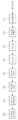
도 1은 본 발명의 일 실시예에 따른 푸리에 변환 기반 페이져 추정 장치에 대한 구성도이다.1 is a block diagram of an apparatus for estimating a Fourier transform based phaser according to an embodiment of the present invention.
도 1을 참조하면, 푸리에 변환 기반 페이져 추정 장치는 샘플링부(110), 샘플링 필터부(120), 분리부(130), DFT부(140), 차분 연산부(150), 차분 필터부(160), 직류 옵셋 연산부(170) 및 페이져 추정부(180)를 포함한다.Referring to FIG. 1, a Fourier transform-based phaser estimating apparatus includes a
샘플링부(110)는 장치로 입력되는 입력 신호, 예를 들어 전류 신호, 전압 신호 등을 샘플링 주파수로 샘플링하여 샘플링된 샘플들을 출력한다.The
이때, 샘플링부(110)는 아날로그 디지털 변환기(ADC)를 포함하는 것이 바람직하고, ADC의 성능은 입력 신호의 한 주기에 대한 샘플들 수 즉, 샘플링 주파수에 따라 달라질 수 있으며, 계측 노이즈를 최소화하기 위해 입력 신호를 두 개의 ADC를 사용하여 서로 반대 부호를 갖도록 샘플링할 수도 있다.In this case, the
여기서, 샘플링부(110)로 입력되는 입력 신호는 장치로 직접 입력되는 신호일 수도 있지만, 아날로그 필터에 의한 필터링된 신호일 수도 있다. 예컨대, 장치로 입력되는 입력 신호가 아날로그 필터에 의해 저역 또는 대역 통과 필터링된 후 샘플링부(110)로 입력될 수 있다.Here, the input signal input to the
샘플링 필터부(120)는 샘플링부(110)에 의해 샘플링된 샘플들을 기 설정된 필터링 주파수로 저역 또는 대역 통과 필터링한다.The
여기서, 샘플링 필터부(120)는 N/4조파(N은 주기당 샘플링 수) 이상의 성분을 제거하는 저역 또는 대역 통과 필터인 것이 바람직하다.Here, the
분리부(130)는 샘플링 필터부(120)에 의해 저역 또는 대역 통과 필터링된 한 주기 데이터의 샘플들을 적어도 두 개 이상의 샘플 그룹들로 분리한다.The separating
이때, 분리부는 한 주기 데이터의 샘플들을 일정 간격을 갖는 샘플 그룹들로 분리할 수 있다. 예컨대, 분리부는 한 주기 데이터의 샘플들을 홀수 샘플 그룹과 짝수 샘플 그룹의 두 샘플 그룹들로 분리하거나, 샘플간의 간격이 일정한 세 개 이상의 그룹들로 분리할 수 있는데, 샘플 수가 N개이고 그룹을 세 개로 분리하는 경우 첫 번째 그룹은 1, 4, 7,..., N-2의 샘플들로 구성되고, 두 번째 그룹은 2, 5, 8,..., N-1의 샘플들로 구성되며, 세 번째 그룹은 3, 6, 9,..., N의 샘플들로 구성될 수 있다.In this case, the separator may separate the samples of one period data into sample groups having a predetermined interval. For example, the separation unit may separate the samples of one period data into two sample groups, an odd sample group and an even sample group, or may be divided into three or more groups having a constant interval between samples, with N samples and three groups. When separated, the first group consists of samples of 1, 4, 7, ..., N-2, and the second group consists of samples of 2, 5, 8, ..., N-1 The third group may consist of samples of 3, 6, 9, ..., N.
이하, 본 발명에서는 한 주기 데이터의 샘플들을 홀수 샘플 그룹(이하, "홀수 샘플"이라 칭함)과 짝수 샘플 그룹(이하, "짝수 샘플"이라 칭함)으로 분리하는 것으로 설명한다.Hereinafter, the present invention will be described as separating samples of one period data into an odd sample group (hereinafter referred to as "odd sample") and an even sample group (hereinafter referred to as "even sample").
DFT부(140)는 분리부(130)에 의해 분리된 홀수 샘플 및 짝수 샘플에 대한 DFT를 수행한다.The
여기서, 홀수 샘플에 대한 DFT 및 짝수 샘플에 대한 DFT를 구하는 과정에 대해 보호 계전기를 예로 하여 설명하면 다음과 같다.Herein, a process of obtaining a DFT for odd samples and a DFT for even samples will be described with reference to the protective relay as an example.
먼저, 보호 계전기에서 측정되는 전류 신호는 <수학식 1>과 같이 표현될 수 있다.First, the current signal measured by the protection relay can be expressed as in Equation 1.

여기서, i[n]은 전류 신호를 말하고, A0 및 τ는 직류 옵셋 성분의 크기 및 시정수를 말하고, Ak 및 φk는 k조파 정현파 성분의 크기 및 위상각을 말하고, △t는 샘플링 간격을 말하고, N은 주기당 샘플링 수를 말한다.Where i [n] is the current signal, A0 and τ are the magnitude and time constant of the DC offset component, Ak and φk are the magnitude and phase angle of the k harmonic sinusoidal component, and Δt is the sampling N is the interval, and N is the number of samples per period.
<수학식 1>과 같은 전류 신호의 DFT에 의한 전력 주파수 성분의 페이져는 <수학식 2>에 의해 계산된다.The phaser of the power frequency component by the DFT of the current signal such as <Equation 1> is calculated by <


여기서, I1thDFT는 전류 신호의 기본파 성분에 대한 DFT를 말하고, IdcDFT는 전류 신호의 직류 옵셋 성분에 대한 DFT를 말하고, E는 직류 옵셋 성분의 지수항을 말한다.Here, I1thDFT refers to the DFT for the fundamental wave component of the current signal, IdcDFT refers to the DFT for the DC offset component of the current signal, and E refers to the exponent term of the DC offset component.
<수학식 2>의 전류 신호에 대한 DFT를 홀수 샘플에 대한 DFT와 짝수 샘플에 대한 DFT로 분해하면 <수학식 3>과 나타낼 수 있고, <수학식 3>을 통해 짝수 샘플에 대한 DFT 및 홀수 샘플에 대한 DFT를 <수학식 4>와 <수학식 5>와 같이 나타낼 수 있다.Decomposing the DFT for the current signal of


DFT부(140)는 <수학식 4> 및 <수학식 5>와 같이 짝수 샘플에 대한 DFT 및 홀수 샘플에 대한 DFT를 수행한다.The
차분 연산부(150)는 DFT부(140)에 의해 수행된 짝수 샘플에 대한 DFT와 홀수 샘플에 대한 DFT의 차분을 연산한다.The
물론, 차분 연산부(150)는 홀수 샘플에 대한 DFT와 짝수샘플에 대한 DFT의 차분을 연산할 수도 있으며, 이는 장치에서 페이져를 연산하는 과정 또는 방법에 따라 달라질 수 있다.Of course, the
여기서, 차분 연산부(150)는 샘플 그룹들이 세 개 이상으로 분리된 경우 분리된 세 개 이상의 그룹들 중 선택된 두 개의 그룹의 차분을 연산하는 것이 바람직하다.Here, when the
이때, 차분 연산부(150)는 <수학식 6>을 이용하여 짝수 샘플에 대한 DFT와 홀수 샘플에 대한 DFT의 차분을 연산할 수 있다.In this case, the

차분 필터부(160)는 <수학식 6>에 의한 짝수 샘플에 대한 DFT와 홀수 샘플에 대한 DFT의 차분 연산에 의해 증폭되는 노이즈를 제거하기 위해 차분을 기 설정된 필터링 주파수로 저역 통과 필터링한다.The
즉, DFT는 고조파 노이즈에 강건한 특성을 가지고 있지만, DFT 차분에 의해 발생될 수 있는 노이즈에 대한 오차를 줄이기 위해 차분 필터부(160)를 사용하는 것이 바람직하다.That is, the DFT is robust to harmonic noise, but it is preferable to use the
직류 옵셋 연산부(170)는 차분 필터부(160)에 의해 저역 통과 필터링된 짝수 샘플에 대한 DFT와 홀수 샘플에 대한 DFT의 차분의 결과를 이용하여 직류 옵셋 성분인 직류 옵셋의 크기 및 지수항을 연산하고, 연산된 직류 옵셋의 지수항을 이용하여 직류 옵셋에 의한 오차(IdcDFT)를 연산한다.The DC offset calculating
여기서, 직류 옵셋 및 직류 옵셋에 의한 오차를 연산하는 과정에 대해 설명한다.Here, the process of calculating the DC offset and the error by the DC offset will be described.
직류 옵셋의 지수항을 연산하기 위해, <수학식 6>에 의해 연산된 차분을 실수부와 허수부로 나누어서 정리하면 <수학식 7>과 <수학식 8>로 나타낼 수 있다.In order to calculate the exponential term of the DC offset, the difference calculated by


직류 옵셋 연산부(170)는 차분에 대한 실수부 및 허수부를 이용하여 직류 옵셋의 지수항을 연산할 수 있다. 즉, <수학식 7>을 <수학식 8>로 나누면 아래 <수학식 9>와 같이 직류 옵셋의 지수항을 연산할 수 있다.The DC offset

즉, 직류 옵셋의 지수항은 차분 연산부(150)에 의해 연산된 짝수 샘플에 대한 DFT와 홀수 샘플에 대한 DFT의 차분(IevenDFT-IoddDFT) 및 주기당 샘플링 수(N)를 통해 연산된다.That is, the exponent term of the DC offset is calculated by the difference between the DFT for the even sample and the DFT for the odd sample (IevenDFT -IoddDFT ) and the number of samplings per period (N) calculated by the
직류 옵셋의 다른 성분인 직류 옵셋의 크기(A0)는 <수학식 9>에 의해 연산된 직류 옵셋의 지수항을 이용하여 <수학식 6>에 의해 연산될 수 있다.The magnitude (A0 ) of the DC offset, which is another component of the DC offset, may be calculated by
상술한 바와 같이, 직류 옵셋 연산부(170)는 <수학식 6> 내지 <수학식 9>를 이용하여 직류 옵셋의 크기 및 지수항을 연산할 수 있다.As described above, the DC offset
또한, 직류 옵셋 연산부(170)는 연산된 직류 옵셋의 지수항을 이용하여 직류 옵셋에 의한 오차 즉, 직류 옵셋의 영향을 연산할 수 있는데, 직류 옵셋에 의한 오차는 <수학식 10>에 의해 연산될 수 있다.In addition, the DC offset

<수학식 10>에서 알 수 있듯이, 직류 옵셋에 의한 오차는 차분 연산부(150)에 의해 연산된 차분, <수학식 9>에 의해 연산된 직류 옵셋의 지수항 및 주기당 샘플링 수(N)를 통해 연산될 수 있다.As can be seen from <
페이져 추정부(180)는 직류 옵셋 연산부(170)에 의해 연산된 직류 옵셋에 의한 오차 및 입력 신호에 대한 DFT를 이용하여 입력 신호에 포함되는 기본파 성분의 페이져를 추정한다.The
즉, 페이져 추정부(180)는 <수학식 11>과 같이 입력 신호에 대한 DFT의 결과(IDFT)에서 직류 옵셋의 영향(IdcDFT)을 제거하면 정확한 전력 주파수 성분 즉, 기본파 성분의 페이져(I1thDFT)를 추정할 수 있다.That is, if the

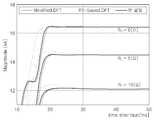
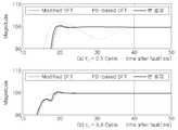
도 2 및 도 3은 본 발명의 푸리에 변환 기반 페이져 추정 장치에 의한 테스트 결과에 대한 예시도들로서, 354[KV], 50[Km]의 가공 송전선로를 EMTP(Electro Magnetic Transient Program)를 이용하여 모델링하고, 최대 크기의 직류 옵셋 성분이 발생하는 고장 투입 위상각 0도 고장을 고려하였으며, 직류 옵셋 성분의 시정수 변화를 고려하기 위해 0[Ω], 5[Ω] 및 10[Ω]의 고장 저항(RF)을 포함하는 10[Km]의 근거리 고장과 40[Km]의 원거리 고장을 모의하고, 모의 파형을 이용하여 본 발명의 테스트 결과를 보인 것이다.2 and 3 are exemplary diagrams of the test results by the Fourier transform-based phaser estimation apparatus of the present invention, modeling the overhead transmission line of 354 [KV], 50 [Km] using the EMTP (Electro Magnetic Transient Program) In addition, the fault input phase angle where the maximum magnitude of the DC offset component is generated is considered to be 0 degrees, and the fault resistances of 0 [Ω], 5 [Ω], and 10 [Ω] are taken into consideration to change the time constant of the DC offset component. The short-range fault of 10 [Km] and the long-range fault of 40 [Km] including (RF ) are simulated, and the test result of the present invention is shown using the simulation waveform.
도 2 및 도 3에서 알 수 있듯이, PS 기반의 DFT 방법은 고장 저항이 없는 경 우에는 직류 옵셋의 영향을 정확하게 제거하고 보다 빠른 수렴 특성을 보이지만 고장 저항이 있는 경우 직류 옵셋의 영향을 완벽하게 제거할 수 없음을 알 수 있다.As can be seen in Figures 2 and 3, the PS-based DFT method accurately removes the effect of DC offset in the absence of fault resistance and shows faster convergence, but completely eliminates the effect of DC offset in the presence of fault resistance. It can be seen that it can not.
또한, 고장 저항이 포함된 고장의 경우 고장 전류에 두 개 이상의 직류 옵셋 성분이 존재하게 되는데, 이 경우 도 2 및 도 3에 도시된 바와 같이 PS 기반의 DFT 방법으로는 직류 옵셋의 영향을 정확하게 제거할 수 없다.In addition, in case of a failure including a fault resistance, two or more DC offset components exist in the fault current. In this case, as shown in FIGS. 2 and 3, the PS-based DFT method accurately removes the influence of the DC offset. Can not.
반면, 본 발명에 따른 푸리에 변환 기반 페이져 추정 장치를 이용하는 경우 고장 저항이 포함된 고장의 경우에도 직류 옵셋의 영향을 완벽하게 제거하여 정확한 기본파 성분의 페이져를 추정할 수 있으며, Modified DFT보다 빠른 수렴 속도를 보임을 알 수 있다.On the other hand, when using the Fourier transform-based phaser estimating apparatus according to the present invention, even in the case of a failure including the fault resistance, it is possible to estimate the phaser of the correct fundamental wave component by completely removing the influence of the DC offset, and converge faster than the modified DFT. You can see the speed.
이와 같이, 본 발명의 일 실시예에 따른 푸리에 변환 기반 페이져 추정 장치는 입력 신호의 한 주기 데이터만을 이용하여 기본파 성분의 페이져를 추정할 수 있을 뿐만 아니라 입력 신호의 홀수 샘플 및 짝수 샘플에 대한 DFT의 차분을 기초로 기본파 성분의 페이져를 추정하기 때문에 하나의 지수 감쇄하는 직류 옵셋 성분만이 아닌 두 개 이상의 지수 감쇄하는 직류 옵셋 성분을 포함하는 입력 신호에 대해서도 기본파 성분의 페이져를 안정적으로 추정할 수 있다.As described above, the Fourier transform-based phaser estimator according to an embodiment of the present invention can estimate the phaser of the fundamental wave component using only one period data of the input signal, as well as the DFT for odd and even samples of the input signal. Since the phaser of the fundamental wave component is estimated based on the difference of, the phaser of the fundamental wave component is stably estimated for an input signal including not only one exponentially decaying DC offset component but also two or more exponentially decaying DC offset components. can do.
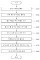
도 4는 본 발명의 일 실시예에 따른 푸리에 변환 기반 페이져 추정 방법에 대한 동작 흐름도이다.4 is a flowchart illustrating an operation of a Fourier transform based pager estimation method according to an embodiment of the present invention.
도 4를 참조하면, 푸리에 변환 기반 페이져 추정 방법은 입력 신호를 아날로그 디지털 변환기(ADC)를 이용하여 샘플링한다(S410).Referring to FIG. 4, in a Fourier transform-based phaser estimation method, an input signal is sampled using an analog-to-digital converter (ADC) (S410).
여기서, 본 발명에 따른 푸리에 변환 기반 페이져 추정 방법은 입력 신호의 한 주기 데이터만을 이용하여 기본파 성분의 페이져를 추정할 수 있기 때문에 한 주기 데이터만을 샘플링하여 사용할 수 있다.Since the Fourier transform-based phaser estimation method according to the present invention can estimate the phaser of the fundamental wave component using only one period data of the input signal, only one period data can be sampled and used.
물론, 입력 신호를 샘플링하는 샘플링 주파수는 입력 신호의 한 주기에서 샘플링하고자 하는 샘플들의 수에 따라 달라질 수 있다.Of course, the sampling frequency for sampling the input signal may vary depending on the number of samples to be sampled in one period of the input signal.
또한, 본 발명에 따른 푸리에 변환 기반 페이져 추정 방법은 도 4에는 도시하지 않았지만, 아날로그 필터를 이용하여 입력 신호를 저역 또는 대역 통과 필터링하는 과정을 수행한 후 샘플링할 수도 있다.In addition, although not illustrated in FIG. 4, the Fourier transform-based phaser estimation method according to the present invention may be sampled after performing a low pass or band pass filtering process on an input signal using an analog filter.
홀수 샘플과 짝수 샘플의 분리에 의해 발생할 수 있는 앨리어싱(aliasing) 현상에 의한 오차를 방지하기 위해 샘플링된 샘플들을 저역 또는 대역 통과 필터링한다(S420).Sampled samples are low pass or band pass filtered to prevent an error due to an aliasing phenomenon that may occur due to separation of odd and even samples (S420).
이때, 샘플들은 N/4조파 이상의 성분이 제거될 수 있는 차단 주파수로 저역 또는 대역 통과 필터링되는 것이 바람직하다.In this case, it is preferable that the samples are low pass or band pass filtered at a cutoff frequency at which components of more than N / 4 harmonics can be removed.
샘플들이 저역 또는 대역 통과 필터링되면, 필터링된 샘플들을 홀수 샘플과 짝수 샘플로 분리한 후 홀수 샘플에 대한 DFT 및 짝수 샘플에 대한 DFT를 각각 수행한다(S430, S440).When the samples are low pass or band pass filtered, the filtered samples are separated into odd and even samples, and then a DFT for odd samples and a DFT for even samples are performed (S430 and S440).
이때, 짝수 샘플에 대한 DFT의 결과 및 홀수 샘플에 대한 DFT의 결과는 상술한 <수학식 4> 및 <수학식 5>와 같이 표현될 수 있다.In this case, the result of the DFT for the even samples and the result of the DFT for the odd samples may be expressed as in
각각 수행된 홀수 샘플에 대한 DFT 및 짝수 샘플에 대한 DFT의 결과를 차분한다. 일 예로, 상술한 <수학식 6>과 같이 짝수 샘플에 대한 DFT의 결과에서 홀수 샘플에 대한 DFT의 결과를 차분 연산한다(S450).The results of the DFTs for the odd samples and the even samples performed for each are differential. For example, as shown in
짝수 샘플에 대한 DFT에서 홀수 샘플에 대한 DFT를 차분 연산하면, 차분 연산에 의해 증폭된 노이즈를 제거하기 위해 연산된 차분을 기 설정된 필터링 주파수 즉, 차단 주파수로 저역 통과 필터링한다(S460).When the DFT for the odd samples is differentially calculated in the DFT for the even samples, low-pass filtering is performed on the calculated difference to remove a noise amplified by the difference operation at a preset filtering frequency, that is, a cutoff frequency (S460).
저역 통과 필터링된 차분 즉, 짝수 샘플에 대한 DFT와 홀수 샘플에 대한 DFT의 차분을 이용하여 직류 옵셋 및 직류 옵셋에 의한 오차를 연산한다(S470).An error due to the DC offset and the DC offset is calculated using the low pass filtered difference, that is, the difference between the DFT for the even sample and the DFT for the odd sample (S470).
여기서, 직류 옵셋의 크기 및 지수항은 상술한 <수학식 6> 및 <수학식 9>를 이용하여 연산할 수 있고, 직류 옵셋에 의한 오차는 상술한 <수학식 10>을 이용하여 연산할 수 있다.Here, the magnitude and exponent term of the DC offset can be calculated using the
단계 S470에 의해 직류 옵셋 및 직류 옵셋에 의한 오차가 연산되면, 연산된 직류 옵셋에 의한 오차 및 입력 신호의 DFT를 이용하여 입력 신호에 포함된 기본파 성분의 페이져를 추정한다(S480).When the error due to the DC offset and the DC offset is calculated in step S470, the pager of the fundamental wave component included in the input signal is estimated using the calculated error of the DC offset and the DFT of the input signal (S480).
이와 같이, 본 발명의 일 실시예에 따른 푸리에 변환 기반 페이져 추정 방법은 입력 신호의 한 주기 데이터의 샘플들을 이용하여 기본파 성분의 페이져를 안정적으로 추정할 수 있고, 두 개 이상의 지수 감쇄하는 직류 옵셋을 포함하는 경우에도 페이져를 정확하게 추정할 수 있다.As described above, the Fourier transform-based phaser estimating method according to an embodiment of the present invention can stably estimate a phaser of fundamental wave components using samples of one period data of an input signal, and offset DC more than two exponentially. Even if it includes a phaser can be accurately estimated.
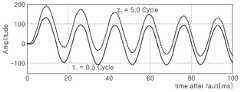
이하, 본 발명의 일 실시예에 따른 푸리에 변환 기반 페이져 추정 방법을 입력 신호에 하나의 직류 옵셋을 포함하는 경우와 두 개의 직류 옵셋을 포함하는 경우에 대해 PS 기반의 DTF 방법 및 Modified DFT 방법과 비교하여 설명한다.Hereinafter, a Fourier transform-based pager estimation method according to an embodiment of the present invention is compared with a PS-based DTF method and a modified DFT method for a case where one DC offset is included in an input signal and two DC offsets. Will be explained.
1) 입력 신호에 포함되는 직류 옵셋이 하나인 경우1) In case of one DC offset included in input signal
여기서, 입력 신호가 <수학식 12>와 같이 표현된다 가정하고 설명한다.Here, it is assumed that the input signal is represented by

<수학식 12>의 입력 신호에 대해 본 발명에 따른 페이져 추정 성능을 확인하기 위해 시정수인 τ1을 0.5 및 5.0 사이클(cycle)로 설정하였으며, 도 5는 τ1에 따른 입력 신호의 파형을 보인 것이다.In order to confirm the pager estimation performance according to the present invention, the time constant τ1 is set to 0.5 and 5.0 cycles with respect to the input signal of
도 6은 도 5에 도시한 입력 신호에 대해 본 발명에 따른 페이져 추정 방법, PS 기반 DFT 방법 및 Modified DFT 방법에 의한 페이져 추정 결과를 보인 것으로, 직류 옵셋 성분이 하나인 경우에는 세 방법 모두 기본파 성분의 페이져를 정확하게 추정하는 것을 알 수 있다.FIG. 6 illustrates a phaser estimation result using the phaser estimation method, the PS-based DFT method, and the modified DFT method according to the present invention with respect to the input signal shown in FIG. 5. It can be seen that the phaser of the component is accurately estimated.
2) 입력 신호에 포함되는 직류 옵셋이 두 개인 경우2) When there are two DC offsets included in the input signal
여기서, 입력 신호가 <수학식 13>과 같이 표현된다 가정하고 설명한다.Here, it is assumed that the input signal is expressed by Equation (13).

도 7은 <수학식 13>의 입력 신호에 대해 시정수 τ2가 20 사이클로 고정된 상태에서 τ1이 0.5 및 5.0 사이클인 경우에 대한 입력 신호의 파형을 보인 것이다.FIG. 7 illustrates waveforms of the input signal for the case where τ1 is 0.5 and 5.0 cycles with the time constant τ2 fixed at 20 cycles for the input signal of Equation (13).
도 8은 도 7에 도시한 입력 신호에 대해 본 발명에 따른 페이져 추정 방법, PS 기반 DFT 방법 및 Modified DFT 방법에 의한 페이져 추정 결과를 보인 것으로, 도시된 바와 같이, τ1이 0.5 사이클인 경우에, PS 기반의 DFT 방법은 입력 신호에 포함된 두 개의 직류 옵셋의 영향을 완벽하게 제거할 수 없다는 것을 알 수 있는데, PS 기반 DFT 방법의 오차는 시정수가 작은 직류 옵셋 성분이 감쇄되어 없어지는 시점에서 발생한다(도 8a).FIG. 8 illustrates a phaser estimation result by the phaser estimation method, the PS-based DFT method, and the modified DFT method according to the present invention with respect to the input signal shown in FIG. 7, when τ1 is 0.5 cycles. The PS-based DFT method cannot completely eliminate the effects of two DC offsets in the input signal. The error of the PS-based DFT method is when the DC offset component with a small time constant is attenuated. Occurs (FIG. 8A).
이는 PS 기반 DFT 방법이 입력 신호의 한 주기 데이터를 홀수 샘플과 짝수 샘플로 나누어 두 개의 적분을 수행하고 적분 결과의 비를 이용하여 직류 옵셋 성분을 추정하기 때문에 두 개의 직류 옵셋 성분이 함께 존재하는 구간과 하나의 직류 옵셋 성분만 존재하는 구간이 하나의 적분 구간 내에 존재하는 경우, 적분 결과의 비로써 직류 옵셋 성분의 시정수 및 크기를 정확하게 추정할 수 없게 된다. 특히, 두 개의 직류 옵셋의 부호가 다르고 크기가 큰 직류 옵셋 성분의 시정수가 작은 경우 위와 같은 현상에 의한 오차가 크게 발생한다.This is because the PS-based DFT method divides one period of the input signal into odd and even samples, performs two integrations, and estimates the DC offset component using the ratio of the integration results. When a section in which only one DC offset component exists and exists in one integral section, the time constant and magnitude of the DC offset component cannot be accurately estimated by the ratio of the integration result. In particular, when the codes of the two DC offsets are different and the time constants of the large DC offset components are small, an error due to the above phenomenon occurs largely.
반면 도 8에 도시된 바와 같이, 본 발명에 따른 페이져 추정 방법 및 Modified DFT 방법의 경우에는 직류 옵셋의 영향을 완벽하게 제거할 수 있는데, 이는 푸리에 변환의 결과를 이용하여 직류 옵셋 성분을 추정하는 경우 두 개의 직류 옵셋이 존재하더라도 하나의 직류 옵셋 성분으로 근사화된 값을 추정할 수 있기 때문이다.On the other hand, as shown in FIG. 8, in the case of the phaser estimation method and the modified DFT method according to the present invention, the influence of the DC offset can be completely eliminated, which is a case of estimating the DC offset component using the result of the Fourier transform. This is because an approximation of one DC offset component can be estimated even if two DC offsets exist.
입력 신호 1) 및 2)에 대한 페이져 추정 결과에서 알 수 있듯이, 본 발명에 따른 페이져 추정 방법은 입력 신호에 포함되는 직류 옵셋이 하나 또는 두 개인 경우에도 기본파 성분의 페이져를 정확하게 추정할 수 있다는 것을 알 수 있다.As can be seen from the phaser estimation results for the input signals 1) and 2), the phaser estimation method according to the present invention can accurately estimate the phaser of the fundamental wave component even when one or two DC offsets are included in the input signal. It can be seen that.
또한, Modified DFT 방법이 푸리에 변환을 위해 입력 신호의 한 주기 데이터 이 외에 두 개의 샘플을 추가적으로 사용하는 반면, 본 발명은 입력 신호의 한 주기 데이터만을 사용하기 때문에 Modified DFT 방법에 비해 보다 빠르게 정확한 기본파 성분의 페이져를 추정할 수 있다.In addition, while the modified DFT method uses two samples in addition to one period data of the input signal for Fourier transform, the present invention uses only one period data of the input signal, so that the accurate fundamental wave is faster than the modified DFT method. The phaser of the component can be estimated.
이와 같이 본 발명의 일 실시예에 따른 푸리에 변환 기반 페이져 추정 방법은 계통 상태 및 고장 조건에 영향을 받지 않고 직류 옵셋의 영향을 제거하여 정확한 기본파 성분의 페이져를 추정할 수 있으므로, 전력 신호의 빠르고 정확한 연산을 필요로 하는 모든 분야에 기여할 수 있다.As described above, the Fourier transform-based phaser estimation method according to an embodiment of the present invention can estimate the phaser of the fundamental fundamental component by removing the influence of the DC offset without being affected by the system state and the fault condition, thereby providing a fast power signal. It can contribute to any field that requires accurate computation.
본 발명에 의한, 지수 감쇄하는 직류 옵셋 영향을 제거한 푸리에 변환 기반 페이져 추정 방법 및 그 장치는 본 발명의 기술적 사상의 범위 내에서 양한 형태로 변형, 응용 가능하며 상기 실시 예에 한정되지 않는다. 또한, 상기 실시 예와 도면은 발명의 내용을 상세히 설명하기 위한 목적일 뿐, 발명의 기술적 사상의 범위를 한정하고자 하는 목적은 아니며, 이상에서 설명한 본 발명은 본 발명이 속하는 기술분야에서 통상의 지식을 가진 자에 있어 본 발명의 기술적 사상을 벗어나지 않는 범위 내에서 여러 가지 치환, 변형 및 변경이 가능하므로 상기 실시 예 및 첨부 된 도면에 한정되는 것은 아님은 물론이며, 후술하는 청구범위뿐만이 아니라 청구범위와 균등 범위를 포함하여 판단되어야 한다.The Fourier transform-based phaser estimation method and apparatus according to the present invention, which eliminates the influence of the exponential decay DC offset, can be modified and applied in various forms within the scope of the technical idea of the present invention and are not limited to the above embodiments. In addition, the embodiments and drawings are merely for the purpose of describing the contents of the invention in detail, not intended to limit the scope of the technical idea of the invention, the present invention described above is common knowledge in the technical field to which the present invention belongs As those skilled in the art can have various substitutions, modifications, and changes within the scope without departing from the spirit of the present invention, it is not limited to the embodiments and the accompanying drawings, of course, and not only the claims to be described below but also the claims. And should be judged to include equality.
도 1은 본 발명의 일 실시예에 따른 푸리에 변환 기반 페이져 추정 장치에 대한 구성도이다.1 is a block diagram of an apparatus for estimating a Fourier transform based phaser according to an embodiment of the present invention.
도 2는 본 발명의 푸리에 변환 기반 페이져 추정 장치에 의한 테스트 결과에 대한 일 예시도이다.2 is a diagram illustrating a test result by the Fourier transform-based phaser estimating apparatus of the present invention.
도 3은 본 발명의 푸리에 변환 기반 페이져 추정 장치에 의한 테스트 결과에 대한 다른 일 예시도이다.Figure 3 is another exemplary view of the test results by the Fourier transform-based phaser estimation apparatus of the present invention.
도 4는 본 발명의 일 실시예에 따른 푸리에 변환 기반 페이져 추정 방법에 대한 동작 흐름도이다.4 is a flowchart illustrating an operation of a Fourier transform based pager estimation method according to an embodiment of the present invention.
도 5는 하나의 직류 옵셋을 포함하는 입력 신호의 시정수 τ1에 따른 입력 신호의 파형도이다.5 is a waveform diagram of an input signal according to time constant τ1 of an input signal including one DC offset.
도 6은 도 5에 도시한 입력 신호에 대해 본 발명에 따른 페이져 추정 방법, PS 기반 DFT 방법 및 Modified DFT 방법에 의한 페이져 추정 결과를 보인 것이다.FIG. 6 illustrates a phaser estimation result of the phaser estimation method, the PS-based DFT method, and the modified DFT method according to the present invention with respect to the input signal shown in FIG. 5.
도 7은 두 개의 직류 옵셋을 포함하는 입력 신호의 시정수 τ2가 20 사이클로 고정된 상태에서 시정수 τ1에 따른 입력 신호의 파형도이다.7 is a waveform diagram of an input signal according to time constant τ1 in a state where time constant τ2 of an input signal including two DC offsets is fixed at 20 cycles.
도 8은 도 7에 도시한 입력 신호에 대해 본 발명에 따른 페이져 추정 방법, PS 기반 DFT 방법 및 Modified DFT 방법에 의한 페이져 추정 결과를 보인 것이다.FIG. 8 illustrates a phaser estimation result of the phaser estimation method, the PS-based DFT method, and the modified DFT method according to the present invention with respect to the input signal shown in FIG. 7.
< 도면의 주요 부분에 대한 부호의 설명 ><Description of Symbols for Main Parts of Drawings>
110: 샘플링부110: sampling unit
120: 샘플링 필터부120: sampling filter unit
130: 분리부130: separator
140: DFT부140: DFT unit
150: 차분 연산부150: difference calculation unit
160: 차분 필터부160: differential filter unit
170: 직류 옵셋 연산부170: DC offset calculator
180: 페이져 추정부180: phaser estimator
Claims (7)
Translated fromKorean


Priority Applications (2)
| Application Number | Priority Date | Filing Date | Title |
|---|---|---|---|
| KR1020080050328AKR100978902B1 (en) | 2008-05-29 | 2008-05-29 | Fourier Transform-Based Phase Estimation Method and Apparatus Eliminating Exponential Attenuation of DC Offset |
| US12/423,223US8145443B2 (en) | 2008-05-29 | 2009-04-14 | Fourier transform-based phasor estimation method and apparatus capable of eliminating influence of exponentially decaying DC offsets |
Applications Claiming Priority (1)
| Application Number | Priority Date | Filing Date | Title |
|---|---|---|---|
| KR1020080050328AKR100978902B1 (en) | 2008-05-29 | 2008-05-29 | Fourier Transform-Based Phase Estimation Method and Apparatus Eliminating Exponential Attenuation of DC Offset |
Publications (2)
| Publication Number | Publication Date |
|---|---|
| KR20090124241A KR20090124241A (en) | 2009-12-03 |
| KR100978902B1true KR100978902B1 (en) | 2010-08-31 |
Family
ID=41380827
Family Applications (1)
| Application Number | Title | Priority Date | Filing Date |
|---|---|---|---|
| KR1020080050328AExpired - Fee RelatedKR100978902B1 (en) | 2008-05-29 | 2008-05-29 | Fourier Transform-Based Phase Estimation Method and Apparatus Eliminating Exponential Attenuation of DC Offset |
Country Status (2)
| Country | Link |
|---|---|
| US (1) | US8145443B2 (en) |
| KR (1) | KR100978902B1 (en) |
Families Citing this family (15)
| Publication number | Priority date | Publication date | Assignee | Title |
|---|---|---|---|---|
| US8098451B2 (en) | 2008-07-28 | 2012-01-17 | Agere Systems Inc. | Systems and methods for variable fly height measurement |
| KR101106120B1 (en)* | 2010-06-04 | 2012-01-20 | 고려대학교 산학협력단 | Signal calibration apparatus and method |
| US8325432B2 (en) | 2010-08-05 | 2012-12-04 | Lsi Corporation | Systems and methods for servo data based harmonics calculation |
| US8300349B2 (en) | 2010-08-05 | 2012-10-30 | Lsi Corporation | Systems and methods for format efficient calibration for servo data based harmonics calculation |
| US8345373B2 (en) | 2010-08-16 | 2013-01-01 | Lsi Corporation | Systems and methods for phase offset based spectral aliasing compensation |
| US8605381B2 (en)* | 2010-09-03 | 2013-12-10 | Lsi Corporation | Systems and methods for phase compensated harmonic sensing in fly height control |
| US8526133B2 (en) | 2011-07-19 | 2013-09-03 | Lsi Corporation | Systems and methods for user data based fly height calculation |
| US9625559B2 (en)* | 2012-10-08 | 2017-04-18 | General Electric Company | Correcting accumulated power in utility meters |
| EP2746785B1 (en)* | 2012-12-19 | 2017-11-01 | Itron Global SARL | Fundamental frequency stability and harmonic analysis |
| US8854756B1 (en) | 2013-05-10 | 2014-10-07 | Lsi Corporation | Systems and methods for mitigating data interference in a contact signal |
| US8937781B1 (en) | 2013-12-16 | 2015-01-20 | Lsi Corporation | Constant false alarm resonance detector |
| US9129632B1 (en) | 2014-10-27 | 2015-09-08 | Avago Technologies General Ip (Singapore) Pte. Ltd. | Loop pulse estimation-based fly height detector |
| CN111417340A (en)* | 2017-12-22 | 2020-07-14 | 森斯弗里有限公司 | Continuous blood pressure measurement |
| EP3736580B1 (en)* | 2019-05-08 | 2023-08-02 | Siemens Energy Global GmbH & Co. KG | Detection of a dc component in an inductive device |
| US11480601B2 (en)* | 2019-09-26 | 2022-10-25 | General Electric Technology Gmbh | Systems and methods to improve distance protection in transmission lines |
Family Cites Families (3)
| Publication number | Priority date | Publication date | Assignee | Title |
|---|---|---|---|---|
| US5224011A (en)* | 1991-04-19 | 1993-06-29 | Gas Research Institute | Multifunction protective relay system |
| US5701080A (en)* | 1995-03-10 | 1997-12-23 | Cooper Industries, Inc. | Method of improving fault current measurement accuracy on electronic reclosure control |
| US7948420B1 (en)* | 2008-06-20 | 2011-05-24 | Arrowhead Center, Inc. | Eliminating the use of anti-aliasing filters in digital relays by oversampling |
- 2008
- 2008-05-29KRKR1020080050328Apatent/KR100978902B1/ennot_activeExpired - Fee Related
- 2009
- 2009-04-14USUS12/423,223patent/US8145443B2/ennot_activeExpired - Fee Related
Non-Patent Citations (1)
| Title |
|---|
| Y.Guo, et al, "Simplified algorithms for removal of the effect of exponentially decaying DC-offset on the Fourier algorithm", IEEE Transactions on Power Delivery, 18권 3호, 2003.7., pp.711-717.* |
Also Published As
| Publication number | Publication date |
|---|---|
| US8145443B2 (en) | 2012-03-27 |
| US20090299666A1 (en) | 2009-12-03 |
| KR20090124241A (en) | 2009-12-03 |
Similar Documents
| Publication | Publication Date | Title |
|---|---|---|
| KR100978902B1 (en) | Fourier Transform-Based Phase Estimation Method and Apparatus Eliminating Exponential Attenuation of DC Offset | |
| US10725085B2 (en) | Method, device and system for determining the fault position of a fault on a line of an electrical power supply network | |
| Sidhu et al. | Discrete-Fourier-transform-based technique for removal of decaying DC offset from phasor estimates | |
| JP6711844B2 (en) | Fault position detection and distance protection device and related method | |
| Habib et al. | A comparative analysis of digital relaying algorithms for the differential protection of three phase transformers | |
| CA2850834A1 (en) | Fault location using traveling waves | |
| JP2013036884A (en) | Insulation monitoring method and insulation monitor | |
| Argüelles et al. | A new method for decaying dc offset removal for digital protective relays | |
| CN115372699A (en) | Adaptive filtering method, adaptive filtering device, fault detection method, electronic device, and medium | |
| CN102623957B (en) | Narrow-band filtering-based variable data window fundamental wave phasor calculation method | |
| CN110514885A (en) | A strong magnetic stealing monitoring method, device and related equipment | |
| CN103823177B (en) | Performance of filter detection method based on THE DESIGN OF WINDOW FUNCTION and system | |
| JP2008154362A (en) | Power system state estimation apparatus and method | |
| Lázaro et al. | Selective estimation of harmonic components in noisy electrical signals for protective relaying purposes | |
| WO2011089421A1 (en) | Apparatus and method for measuring a phasor of an electrical power system signal | |
| Eisa et al. | Removal of decaying DC offset in current signals for power system phasor estimation | |
| KR100758492B1 (en) | Frequency Estimation System Using Orthogonal Filter and Its Method | |
| EP0214483A1 (en) | Method for measuring distance in digital distance relays | |
| Hwang | Improvement of phasor estimation accuracy by prony-based identification of two decaying dc components | |
| Domínguez et al. | New quick-convergence invariant digital filter for phasor estimation | |
| Hajimahani et al. | Data window selection for removal of decaying DC component in current phasor estimation for distance protection | |
| EP3795966A1 (en) | Circuit interrupter and method of estimating a temperature of a busbar in a circuit interrupter | |
| Pajuelo et al. | An improved voltage phasor estimation technique to minimize the impact of CCVT transients in distance protection | |
| JPH08331752A (en) | Detecting method of ground fault | |
| KR100232764B1 (en) | Apparatus and method for measuring impedance of a digital distance relay |
Legal Events
| Date | Code | Title | Description |
|---|---|---|---|
| A201 | Request for examination | ||
| PA0109 | Patent application | St.27 status event code:A-0-1-A10-A12-nap-PA0109 | |
| PA0201 | Request for examination | St.27 status event code:A-1-2-D10-D11-exm-PA0201 | |
| PN2301 | Change of applicant | St.27 status event code:A-3-3-R10-R13-asn-PN2301 St.27 status event code:A-3-3-R10-R11-asn-PN2301 | |
| PG1501 | Laying open of application | St.27 status event code:A-1-1-Q10-Q12-nap-PG1501 | |
| E902 | Notification of reason for refusal | ||
| PE0902 | Notice of grounds for rejection | St.27 status event code:A-1-2-D10-D21-exm-PE0902 | |
| P11-X000 | Amendment of application requested | St.27 status event code:A-2-2-P10-P11-nap-X000 | |
| P13-X000 | Application amended | St.27 status event code:A-2-2-P10-P13-nap-X000 | |
| E701 | Decision to grant or registration of patent right | ||
| PE0701 | Decision of registration | St.27 status event code:A-1-2-D10-D22-exm-PE0701 | |
| GRNT | Written decision to grant | ||
| PR0701 | Registration of establishment | St.27 status event code:A-2-4-F10-F11-exm-PR0701 | |
| PR1002 | Payment of registration fee | St.27 status event code:A-2-2-U10-U11-oth-PR1002 Fee payment year number:1 | |
| PG1601 | Publication of registration | St.27 status event code:A-4-4-Q10-Q13-nap-PG1601 | |
| FPAY | Annual fee payment | Payment date:20131010 Year of fee payment:4 | |
| PR1001 | Payment of annual fee | St.27 status event code:A-4-4-U10-U11-oth-PR1001 Fee payment year number:4 | |
| FPAY | Annual fee payment | Payment date:20141110 Year of fee payment:5 | |
| PR1001 | Payment of annual fee | St.27 status event code:A-4-4-U10-U11-oth-PR1001 Fee payment year number:5 | |
| FPAY | Annual fee payment | Payment date:20150805 Year of fee payment:6 | |
| PR1001 | Payment of annual fee | St.27 status event code:A-4-4-U10-U11-oth-PR1001 Fee payment year number:6 | |
| FPAY | Annual fee payment | Payment date:20160728 Year of fee payment:7 | |
| PR1001 | Payment of annual fee | St.27 status event code:A-4-4-U10-U11-oth-PR1001 Fee payment year number:7 | |
| L13-X000 | Limitation or reissue of ip right requested | St.27 status event code:A-2-3-L10-L13-lim-X000 | |
| U15-X000 | Partial renewal or maintenance fee paid modifying the ip right scope | St.27 status event code:A-4-4-U10-U15-oth-X000 | |
| FPAY | Annual fee payment | Payment date:20170803 Year of fee payment:8 | |
| PR1001 | Payment of annual fee | St.27 status event code:A-4-4-U10-U11-oth-PR1001 Fee payment year number:8 | |
| FPAY | Annual fee payment | Payment date:20180810 Year of fee payment:9 | |
| PR1001 | Payment of annual fee | St.27 status event code:A-4-4-U10-U11-oth-PR1001 Fee payment year number:9 | |
| FPAY | Annual fee payment | Payment date:20190827 Year of fee payment:10 | |
| PR1001 | Payment of annual fee | St.27 status event code:A-4-4-U10-U11-oth-PR1001 Fee payment year number:10 | |
| R18-X000 | Changes to party contact information recorded | St.27 status event code:A-5-5-R10-R18-oth-X000 | |
| PN2301 | Change of applicant | St.27 status event code:A-5-5-R10-R13-asn-PN2301 St.27 status event code:A-5-5-R10-R11-asn-PN2301 | |
| PR1001 | Payment of annual fee | St.27 status event code:A-4-4-U10-U11-oth-PR1001 Fee payment year number:11 | |
| R18-X000 | Changes to party contact information recorded | St.27 status event code:A-5-5-R10-R18-oth-X000 | |
| PR1001 | Payment of annual fee | St.27 status event code:A-4-4-U10-U11-oth-PR1001 Fee payment year number:12 | |
| PC1903 | Unpaid annual fee | St.27 status event code:A-4-4-U10-U13-oth-PC1903 Not in force date:20220825 Payment event data comment text:Termination Category : DEFAULT_OF_REGISTRATION_FEE | |
| K11-X000 | Ip right revival requested | St.27 status event code:A-6-4-K10-K11-oth-X000 | |
| PC1903 | Unpaid annual fee | St.27 status event code:N-4-6-H10-H13-oth-PC1903 Ip right cessation event data comment text:Termination Category : DEFAULT_OF_REGISTRATION_FEE Not in force date:20220825 | |
| PR0401 | Registration of restoration | St.27 status event code:A-6-4-K10-K13-oth-PR0401 | |
| R401 | Registration of restoration | ||
| PR1001 | Payment of annual fee | St.27 status event code:A-4-4-U10-U11-oth-PR1001 Fee payment year number:13 | |
| PC1903 | Unpaid annual fee | St.27 status event code:A-4-4-U10-U13-oth-PC1903 Not in force date:20230825 Payment event data comment text:Termination Category : DEFAULT_OF_REGISTRATION_FEE | |
| PC1903 | Unpaid annual fee | St.27 status event code:N-4-6-H10-H13-oth-PC1903 Ip right cessation event data comment text:Termination Category : DEFAULT_OF_REGISTRATION_FEE Not in force date:20230825 |