KR100975808B1 - PCB inspection jig - Google Patents
PCB inspection jigDownload PDFInfo
- Publication number
- KR100975808B1 KR100975808B1KR1020080023783AKR20080023783AKR100975808B1KR 100975808 B1KR100975808 B1KR 100975808B1KR 1020080023783 AKR1020080023783 AKR 1020080023783AKR 20080023783 AKR20080023783 AKR 20080023783AKR 100975808 B1KR100975808 B1KR 100975808B1
- Authority
- KR
- South Korea
- Prior art keywords
- contact
- contactor
- connection electrode
- guide plate
- guide hole
- Prior art date
- Legal status (The legal status is an assumption and is not a legal conclusion. Google has not performed a legal analysis and makes no representation as to the accuracy of the status listed.)
- Expired - Fee Related
Links
Images


Classifications
- G—PHYSICS
- G01—MEASURING; TESTING
- G01R—MEASURING ELECTRIC VARIABLES; MEASURING MAGNETIC VARIABLES
- G01R31/00—Arrangements for testing electric properties; Arrangements for locating electric faults; Arrangements for electrical testing characterised by what is being tested not provided for elsewhere
- G01R31/28—Testing of electronic circuits, e.g. by signal tracer
- G01R31/2801—Testing of printed circuits, backplanes, motherboards, hybrid circuits or carriers for multichip packages [MCP]
- G—PHYSICS
- G01—MEASURING; TESTING
- G01R—MEASURING ELECTRIC VARIABLES; MEASURING MAGNETIC VARIABLES
- G01R1/00—Details of instruments or arrangements of the types included in groups G01R5/00 - G01R13/00 and G01R31/00
- G01R1/02—General constructional details
- G01R1/06—Measuring leads; Measuring probes
- G01R1/067—Measuring probes
- G01R1/073—Multiple probes
- G01R1/07307—Multiple probes with individual probe elements, e.g. needles, cantilever beams or bump contacts, fixed in relation to each other, e.g. bed of nails fixture or probe card
- G01R1/07314—Multiple probes with individual probe elements, e.g. needles, cantilever beams or bump contacts, fixed in relation to each other, e.g. bed of nails fixture or probe card the body of the probe being perpendicular to test object, e.g. bed of nails or probe with bump contacts on a rigid support
- G01R1/07328—Multiple probes with individual probe elements, e.g. needles, cantilever beams or bump contacts, fixed in relation to each other, e.g. bed of nails fixture or probe card the body of the probe being perpendicular to test object, e.g. bed of nails or probe with bump contacts on a rigid support for testing printed circuit boards
- G—PHYSICS
- G01—MEASURING; TESTING
- G01R—MEASURING ELECTRIC VARIABLES; MEASURING MAGNETIC VARIABLES
- G01R31/00—Arrangements for testing electric properties; Arrangements for locating electric faults; Arrangements for electrical testing characterised by what is being tested not provided for elsewhere
- G01R31/28—Testing of electronic circuits, e.g. by signal tracer
- G01R31/2851—Testing of integrated circuits [IC]
- G01R31/2886—Features relating to contacting the IC under test, e.g. probe heads; chucks
- H—ELECTRICITY
- H05—ELECTRIC TECHNIQUES NOT OTHERWISE PROVIDED FOR
- H05K—PRINTED CIRCUITS; CASINGS OR CONSTRUCTIONAL DETAILS OF ELECTRIC APPARATUS; MANUFACTURE OF ASSEMBLAGES OF ELECTRICAL COMPONENTS
- H05K1/00—Printed circuits
- H05K1/02—Details
- H05K1/0266—Marks, test patterns or identification means
- H05K1/0268—Marks, test patterns or identification means for electrical inspection or testing
Landscapes
- Engineering & Computer Science (AREA)
- Microelectronics & Electronic Packaging (AREA)
- Physics & Mathematics (AREA)
- General Physics & Mathematics (AREA)
- Computer Hardware Design (AREA)
- General Engineering & Computer Science (AREA)
- Measuring Leads Or Probes (AREA)
Abstract
Translated fromKoreanDescription
Translated fromKorean본 발명은, 피검사 기판을 검사하는 경우에 사용되는 기판검사용 치구에 관한 것으로서, 더 상세하게는, 기판검사용 치구의 접촉자(接觸子)와 기판검사용 치구의 전극부의 접촉저항을 저감(低減)시키는 기판검사용 치구의 전극구조를 구비하는 기판검사 치구(基板檢査 治具)에 관한 것이다.BACKGROUND OF THE
또한 본 발명은, 프린트 배선기판에 한하지 않고, 예를 들면 플렉시블 기판, 다층배선 기판, 액정 디스플레이나 플라즈마 디스플레이용의 전극판 및 반도체 패키지용의 패키지 기판이나 필름 캐리어 등 다양한 기판에 있어서의 전기적 배선의 검사에 적용할 수 있고, 본 명세서에서는 이러한 여러 가지의 배선기판을 총칭해서 「기판」이라고 한다.In addition, the present invention is not limited to printed wiring boards, but for example, flexible wiring boards, multilayer wiring boards, electrode boards for liquid crystal displays or plasma displays, and electrical wiring in various substrates such as package substrates and film carriers for semiconductor packages. It can be applied to the inspection of, and in this specification, these various wiring boards are collectively referred to as "substrate".
종래에 회로기판 상에 형성되는 배선 패턴은, 그 회로기판에 탑재되는 IC 등의 반도체나 저항기 등의 전기·전자부품에 전기신호를 정확하게 전달할 필요가 있기 때문에, 전기·전자부품을 실장(實裝)하기 전의 프린트 배선기판, 액정 패널이나 플라즈마 디스플레이 패널에 배선 패턴이 형성된 회로 배선기판 또는 반도체 웨이퍼 등의 기판에 형성된 배선 패턴에 대하여, 검사대상이 되는 배선 패턴에 구비된 검사점 사이의 저항값을 측정하여 그 양부(良否)가 판정되고 있었다.In the conventional wiring pattern formed on a circuit board, it is necessary to accurately transmit electrical signals to electrical / electronic parts such as semiconductors and resistors such as ICs mounted on the circuit board. The resistance value between the inspection points provided in the wiring pattern to be inspected is measured with respect to the wiring pattern formed on the printed wiring board, the circuit wiring board having the wiring pattern formed on the liquid crystal panel or the plasma display panel, or the semiconductor wafer. It measured and the quality was judged.
이러한 판정 검사에는 배선 패턴의 단선 및 단락을 검사하는 검사방법이 실시되고 있다. 이러한 도통(導通)이나 단락의 검사에서는, 검사대상이 되는 배선 패턴의 2부분에 설치되는 검사점에, 각각 1개씩 측정 단자를 접촉시키고 그 측정 단자 사이에 소정의 레벨의 측정용 전류를 흘림으로써 그 측정 단자 사이의 전압치를 측정하고, 이 전압치와 미리 정해진 임계치를 비교함으로써 양부의 판정이 이루어지고 있었다.In this determination inspection, an inspection method for inspecting disconnection and short circuit in the wiring pattern is implemented. In the inspection of such conduction or short circuit, each of the measurement terminals is brought into contact with each of the inspection points provided on two portions of the wiring pattern to be inspected, and a current of a predetermined level is measured between the measurement terminals. The determination was made by measuring the voltage value between the measurement terminals and comparing this voltage value with a predetermined threshold value.
그러나 이러한 방법에서 사용되는 기판검사용 치구에서는, 배선 패턴의 2부분의 검사점 각각에 1개씩 접촉시킨 측정 단자를 측정용 전류의 공급과 전압의 측정에 공용하는 경우에는, 측정 단자와 검사점 사이의 접촉저항이 측정 전압에 영향을 주어서, 저항값의 측정 정밀도가 저하되고 검사결과의 신뢰성이 저하된다는 단점이 있었다.However, in the board inspection jig used in such a method, when a measurement terminal in contact with each of the two inspection points of the wiring pattern is connected to the supply of the measurement current and the measurement of the voltage, between the measurement terminal and the inspection point The contact resistance of has a disadvantage in that the measurement voltage affects the measurement voltage, thereby reducing the measurement accuracy of the resistance value and reducing the reliability of the test result.
특히 최근에는, 회로기판 상에 형성되는 배선 패턴의 미세화가 진행되고 배선 패턴의 저항값이 작아지고 있어서, 상기한 접촉저항이 상기 측정치에 미치는 영향이 큰 문제가 되고 있었다.In particular, in recent years, the miniaturization of wiring patterns formed on circuit boards has progressed and the resistance value of wiring patterns has become small, and the influence of the above-mentioned contact resistance on the measured value has become a big problem.
이러한 접촉저항의 문제를 해결하기 위해서, 특허문헌1에 개시된 것 같은 접촉자가 제안되어 있다. 상기 접촉자는, 측정대상의 전극에 대하여 대략 수직으로 접촉 가능한 대략 직선 모양의 접촉부를 구비하고 있고, 이 접촉부의 길이방향을 따라 연장되는 일부가 당해 접촉부의 다른 부분과 다른 열팽창율을 구비하는 재료로 구성되어 있다. 이렇게 구성됨으로써 접촉부가 바이메탈로 되어 있으므로, 소정의 환경온도 하에서 접촉부를 측정대상의 전극에 대략 수직으로 접촉시키고 그 상태에서 오버드라이브(overdrive)를 하면, 당해 측정대상의 전극으로부터 전달되는 환경온도의 열에 의하여 당해 접촉부가 작은 열팽창율의 소재로 구성된 부분을 향해서 만곡하게 된다.In order to solve such a problem of contact resistance, a contactor as disclosed in
특허문헌1 : 일본국 공개특허공보 특개 2005-345129호 공보Patent Document 1: Japanese Unexamined Patent Publication No. 2005-345129
그러나 특허문헌1에 기재된 접촉자를 사용하여도, 전극부에 대하여 수직으로 접촉시키는 것을 가능하게 할 뿐으로서, 접촉 안정성이라는 견지로부터 감안하면, 충분한 접촉 안정성을 구비하여 접촉 저항값이 낮은 접속을 구비하고 있다고는 말할 수 없었다.However, even when using the contactor described in
또한 기판검사 치구는 그 사용 횟수가 수 만회∼수 십만회까지도 된다. 이 때문에, 사용할 때에 기판검사용 접촉자가 파손 또는 마모되었을 경우에는 신속하고 간편하게 교환할 필요가 있었다.In addition, the board | substrate inspection jig may be used from tens of thousands to several hundred thousand times. For this reason, when the contactor for board | substrate test | inspection was broken or worn at the time of use, it was necessary to replace it quickly and easily.
본 발명은, 이러한 실정을 감안하여 이루어진 것으로서, 유지보수성이 우수함과 아울러 기판검사용 치구의 접촉자와 기판검사용 치구의 전극부의 접촉저항을 저감시키는 전극구조를 구비하는 기판검사 치구를 제공한다.SUMMARY OF THE INVENTION The present invention has been made in view of such circumstances, and provides a substrate inspection jig having an electrode structure which is excellent in maintainability and which reduces contact resistance of the contact portion of the substrate inspection jig and the electrode portion of the substrate inspection jig.
청구항1에 기재된 발명은, 피검사 기판의 전기적 특성을 검사하기 위해서, 기판검사장치 본체와 상기 피검사 기판의 배선 패턴에 형성되는 복수의 기판 피검사점과의 사이의 전기적 도통을 얻기 위한 기판검사용 치구로서, 상기 기판검사용 치구는, 양단에 전기적 도통을 도모하는 단부를 구비하고, 일방의 단부가 상기 기판 피검사점의 하나에 압접되고 도전성을 구비함과 아울러 상기 단부를 제외하고 가장자리에 절연부를 구비하는 막대 모양의 복수의 접촉자와, 상기 복수의 접촉자를 지지함과 아울러, 상기 접촉자의 일방의 단부를 상기 검사점으로 안내하는 제1안내구멍을 구비하는 제1안내판과, 상기 접촉자의 타방의 단부를 상기 기판검사장치의 전극부로 안내하는 제2안내구멍을 구비하는 제2안내구멍을 구비하는 접촉자 지지체와, 상기 접촉자의 각각의 접촉자의 타방의 단부와 대향해서 배치됨과 아울러 상기 기판검사장치에 접속되는 접속 전극부를 구비하는 접속 전극체를 구비하고, 상기 제1안내구멍은, 상기 접촉자의 절연부의 지름보다 작은 지름을 구비하도록 형성되고, 상기 제2안내구멍은, 상기 접촉자의 절연부의 지름보다 큰 지름을 구비하도록 형성되고, 상기 제1안내판과 상기 제2안내판은, 상기 접촉자를 탈착 가능하게 하기 위해서, 상기 제1안내구멍과 그에 대응하는 상기 제2안내구멍이 정합하는 정합상태와, 상기 접촉자를 지지하기 위해서, 상기 정합상태로부터 상기 제2안내판이 상기 제2안내판의 평면방향으로 이동하는 지지상태를 구비하고, 상기 접촉자의 상기 타방의 단부와 상기 접속 전극체가 접속하는 때에 있어서, 각각의 상기 타방의 단부의 근방의 측주면의 적어도 일부가, 이와 대향하는 상기 접속 전극부의 일부와 접촉함으로써 전기적으로 도통상태가 되는 것을 특징으로 하는 기판검사용 치구를 제공한다.Invention of
청구항2의 발명은, 상기 접속 전극부는, 이것과 대향하는 상기 접촉자의 상기 타방의 단부를 내부에 수용하는 구조를 구비하고, 또한 상기 접촉자와 상기 접속 전극부의 도통상태는, 적어도 상기 접촉자의 타방의 단부와 상기 접속 전극부의 내부측 표면의 접촉에 의한 것을 특징으로 하는 청구항1에 기재된 기판검사용 치구를 제공한다.The invention according to
청구항3의 발명은, 상기 접속 전극부는, 이들과 대향하는 상기 접촉자의 상기 타방의 단부의 적어도 일부를 느슨하게 삽입할 수 있는 통모양인 것을 특징으로 하는 청구항1 또는 2에 기재된 기판검사용 치구를 제공한다.The invention according to
청구항4에 기재된 발명은, 상기 접촉자의 절연부와 상기 타방의 단부의 경계는, 상기 제2안내구멍으로부터 내측에 배치되는 것을 특징으로 하는 청구항1에 기재된 기판검사용 치구.The invention according to
청구항5에 기재된 발명은, 상기 접촉자 지지체는, 상기 접촉자의 타방이 상기 접속 전극부에 접촉되는 사용시에 있어서, 상기 접촉자가 돌출되도록, 상기 접촉자의 장축방향으로 슬라이드 하는 보호부를 구비하여 이루어지는 것을 특징으로 하는 청구항1에 기재된 기판검사용 치구를 제공한다.The invention according to claim 5 is characterized in that the contact supporter includes a protection portion that slides in the long axis direction of the contact so that the contact is protruded when the other of the contact is in contact with the connection electrode portion. Provided is a substrate inspection jig according to
청구항1에 기재된 발명에 의하면, 제1안내판과 제2안내판을 사용하여 접촉자를 탈착가능한 정합상태와 지지가능한 지지상태를 구비하도록 형성되어 있으므로, 접촉자의 교환을 하는 경우에는 제1안내판과 제2안내판을 정합상태로 함으로써 용이하게 교환할 수 있다.According to the invention as set forth in
또한 접촉자군의 타방의 단부와 접속 전극체를 접속함에 있어서, 접촉자의 타방의 단부의 근방의 측주면의 적어도 일부가 이와 대향하는 접속 전극부의 일부와 접촉함으로써 전기적으로 도통상태가 되므로, 접촉자와 접속 전극부의 접촉 저항값을 저감시킬 수 있음과 아울러 사용 횟수에 관계없이 안정된 접촉 저항값을 구비하는 기판검사용 치구를 제공한다.Moreover, in connecting the other end part of a contact group and a connection electrode body, since at least one part of the side peripheral surface of the vicinity of the other end part of a contactor contacts and contacts a part of the connection electrode part which opposes, it connects with a contactor, Provided is a substrate inspection jig that can reduce the contact resistance value of the electrode portion and has a stable contact resistance value regardless of the number of times of use.
청구항2의 발명에 의하면, 접촉자와 접속 전극부의 도통상태가, 적어도 접촉자의 타방의 단부와 접속 전극부의 내부측 표면의 접촉에 의하므로, 접촉자와 접속 전극부의 접촉 면적을 크게 할 수 있어, 접촉 저항값을 보다 저감시킬 수 있음과 아울러 사용 횟수에 관계없이 안정된 접촉 저항값을 구비하는 기판검사용 치구를 제공한다.According to the invention of
청구항3의 발명에 의하면, 접속 전극부가 접촉자를 느슨하게 삽입할 수 있는 형상이므로, 접촉자가 접속 전극부에 출입할 때에 지나친 부담이 걸리는 것을 방지할 수 있다.According to the invention of
또한 접속 전극부가 통 모양으로 형성되어 있기 때문에, 접촉자가 접촉하는 접촉면을 균일하게 할 수 있어서 어느 통부에 접촉하여도 안정된 접촉 저항값을 가지는 기판검사용 치구를 제공한다.Moreover, since the connection electrode part is formed in a cylindrical shape, the contact surface with which a contactor contacts can be made uniform, and the board | substrate inspection jig which has a stable contact resistance value in contact with any cylinder part is provided.
청구항4에 기재된 발명에 의하면, 제1안내판과 제2안내판이 정합상태에 있는 경우에, 접촉자의 절연부와 타방의 단부의 경계가 제2안내구멍의 측면을 형성하는 제2안내구멍에 접촉하여 결합하게 되어, 접촉자의 낙하나 어긋남을 방지할 수 있다.According to the invention as set forth in
청구항5에 기재된 발명에 의하면, 접촉자 지지체가 접촉자를 보호하는 보호부를 구비하기 때문에, 접촉자의 사용시와 미사용시에 있어서 효과적으로 접촉자를 보호할 수 있고, 접촉자의 사용 수명을 연장시킬 수 있는 기판검사용 치구를 제공한다.According to the invention as set forth in claim 5, since the contact support includes a protection portion for protecting the contact, it is possible to effectively protect the contact at the time of use and non-use of the contact, and to increase the service life of the contact. To provide.
[실시예][Example]
본 발명의 실시예를 설명한다.An embodiment of the present invention will be described.
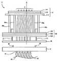
도1은, 본 발명에 관한 기판검사용 치구를 사용하는 경우의 개략적인 구성을 나타내고 있다. 이 도1에서는, 복수의 접촉자101, 이러한 접촉자101을 여러 개의 바늘 모양으로 지지하는 지지체102, 상기 지지체102를 지지함과 아울러 접촉자101과 접촉하여 도통이 되는 접속 전극부를 구비하는 접속 전극체103, 검출되는 전기신호를 처리하는 검사신호 처리부104 및 검사용 접촉자101과 검사신호 처리부104를 접속하는 와이어 케이블105를 나타내고 있다. 접촉자101은 피검사 기판에 형성되는 배선 패턴의 각 검사점에 접촉하는 단자이고, 접속 전극체103은 접촉자101과 검사신호 처리부104의 피치 변환을 실행하여 전기적으로 접속한다.1 shows a schematic configuration in the case of using the jig for inspection of a substrate according to the present invention. In Fig. 1, a plurality of
접속 전극체103은, 지지체102의 배치측에 접촉자101과 전기적으로 접속하는 접속 전극부106을 구비하고 있다. 본 발명은, 상기 접속 전극부106을 창의적으로 고안함으로써 접촉자101과의 접속 저항값을 저감시킬 수 있음과 아울러 안정성을 구비한 접속 저항값을 제공한다.The connecting
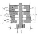
본 발명에 관한 하나의 실시예의 기판검사용 치구1은, 접촉자2, 접촉자 지지체3과 접속 전극체4를 구비하여 이루어진다(도2 참조). 또한 접속 전극체4는, 상기와 같은 검사신호 처리부104와 접속되어 있지만 상기 도2에서는 생략하고 있다. 또한 상기 도2에서는, 기판검사용 치구의 헤드11과 접속 전극체4는 접속되어 있지 않은 상태를 나타내고 있다.The board | substrate inspection jig |
접촉자2는, 가요성(可撓性) 및 도전성(導電性)을 구비하고, 바늘 모양이나 긴 자 모양 등의 막대 모양으로 형성되어 있다. 상기 접촉자2는, 일방이 피검사 기판의 검사점에 압접되고 타방이 후술하는 접속 전극부와 접촉된다. 이 때문에 접촉자2는 검사신호 처리부104로부터의 전기신호를 검사점으로 송신함과 아울러 검사점으로부터의 전기신호를 검사신호 처리부104로 송신할 수 있다.The
상기 접촉자2는 가요성을 구비하고 있기 때문에, 후술하는 접촉자 지지체3의 내부에 형성되는 공간에서 접촉자2의 장축방향에 대하여 직각방향으로 휘게(버클링 하게) 된다. 이 때문에 상기 접촉자2가 사용되는 경우에는, 피검사 기판의 검사점이나 접속 전극부에서의 하중을 받아서 휘고, 이 휨에 의하여 각 접촉부에 대하여 압력이 발생하게 된다.Since the
접촉자2는, 상기와 같은 형상으로 형성되면 특별히 한정되지 않지만, 도3에 나타내는 것 같은 실시예와 같이 형성할 수도 있다.The
상기 도3에 나타낸 접촉자2는, 도3(a)에 나타나 있는 바와 같이 양 쪽 선단이 좁아지는 형상으로 하는 가늘고 긴 막대 모양 부재21로 형성된다. 좁아지는 형상은, 도3(a)에 나타낸 것 같은 첨예형상(尖銳形狀)으로 하여도 좋고 구상형상(球狀形狀)으로 하여도 좋다.The
상기 막대 모양 부재21은, 스테인레스강, 베릴륨 동(beryllium copper)(BeCu)이나 텅스텐(W)을 들 수 있지만, 특별히 한정되는 것이 아니라 도전 물질(導電 物質)이면 된다.The rod-shaped
상기 막대 모양 부재21은, 후술하는 접속 전극부에 접촉하는 접촉 면적에 균일한 하중이 걸리도록 원통이나 원기둥 모양으로 형성되는 것이 바람직하지만 특별하게 한정되는 것은 아니다.The rod-shaped
막대 모양부재21의 길이나 굵기는 특별하게 한정되는 것이 아니라 피검사 기판에 형성되는 배선 패턴의 피치나 피검사 기판의 크기에 따라 적당하게 설정된다.The length and thickness of the rod-shaped
도3(b)에서는 막대 모양 부재21을 통 모양 부재22에 수용한 상태를 나타내고 있다. 상기 통 모양 부재22는 가요성 및 도전성을 구비하고 있다. 막대 모양 부재21이 상기 통 모양 부재22에 삽입된다. 도3(b)에서는 통 모양 부재22의 일방의 선단인 일단22a와 타방의 선단인 타단22b를 비교하였을 경우에 일단22a로부터 돌출되는 막대 모양 부재21의 길이가 타단22b로부터 돌출되는 막대 모양 부재21의 길이보다 길게 되도록 설정되어 있다.3B shows a state where the rod-shaped
상기와 같은 경우에 일단22a는 접속 전극부에 접촉하고, 타단22b는 피검사 기판의 검사점에 접촉하게 된다. 이렇게 배치의 길이를 변화시킴으 로써 막대 모양 부재21이 접속 전극부와 접촉하는 접촉 면적을 크게 할 수 있고 또한 타단22b로부터 막대 모양 부재21이 돌출되는 길이가 짧게 설정되기 때문에, 범프 등의 검사점에 접촉자가 접촉할 때에 통 모양 부재22가, 막대 모양 부재21이 필요 이상으로 검사점에 관입(貫入)되는 것을 방지하는 스토퍼적인 역할을 달성할 수 있음과 아울러 구(球) 모양의 범프 등의 검사점에 대하여 안정되게 접촉할 수 있다. 또한 막대 모양 부재21의 선단형상(先端形狀)의 가공성(加工性)에 의존하지 않고 막대 모양 부재21과 통 모양 부재22에 의한 검사점에 대한 접촉을 가능하게 할 수 있다.In such a case, one
또한 상기 타단22b측의 막대 모양 부재21의 돌출량은, 상기와 같이 일단22a보다 짧게 설정할 수 있음과 동시에 상기 설명과 같이 검사점에 관입되는 양(길이)으로서 설정할 수도 있다.The protruding amount of the rod-shaped
상기 통 모양 부재22는, 막대 모양 부재21을 내부에 수용할 수 있고 막대 모양 부재21과 도통상태가 될 수 있는 크기이면 특별하게 한정되지 않는다.The
통 모양 부재22와 막대 모양 부재21은 서로 전기적으로 접속되어 있다. 이 때문에 막대 모양 부재21을 통 모양 부재22에 삽입한 상태(도3(b)에 나타낸 상태)에서 전체에 전해 도금 또는 무전해 도금을 실시함으로써 형성한다.The
다른 방법으로서, 통 모양 부재22 내부에 돌출 모양부(도면에는 나타내지 않는다)를 복수 형성함으로써, 통 모양 부재22가 막대 모양 부재21을 가압하는 코킹 구조(caulking 構造)를 구비함으로써, 접촉하여 전기적으로 도통시 킬 수 있다.Alternatively, by forming a plurality of protruding portions (not shown in the drawing) inside the
도3(c)에서는, 막대 모양 부재21과 통 모양 부재22가 일체화되고 통 모양 부재22의 겉의 원주면에 절연부23이 형성되어 있다. 상기 절연부23이 형성되는 장소는, 도3(c)에 나타나 있는 바와 같이 접촉자2의 일방단(一方端)과 타방단(他方端) 이외의 장소에 형성된다. 또한 상기 절연부23과 통 모양 부재22에 의하여 형성되는 단차24는, 후술하는 접촉자 지지체3에 접촉자2가 배치되었을 때의 결합부로서 사용되게 된다.In Fig. 3 (c), the rod-
상기 절연부23은, 접촉자2가 휘었을 때에 인접하는 접촉자2와 접촉하여도 단락되는 것을 방지하고 있다.The
상기 절연부23은, 폴리우레탄을 사용할 수 있지만 특별하게 한정되는 것은 아니다.Polyurethane may be used for the insulating
상기 설명에서는, 막대 모양 부재21과 통 모양 부재22와 절연부23을 사용하여 접촉자2를 구성하였을 경우를 설명했지만, 막대 모양 부재21과 절연부23으로 이루어지는 접촉자를 사용하여도 좋으며 접촉자의 구조는 이들에 한정되는 것은 아니다.In the above description, the case where the
또한 본 명세서에서는, 접속 전극부41에 수용되는 접촉자2의 일부를 부호 2A로서 설명하지만, 상기 접촉자2의 수용부2A는 절연부23이 형성되어 있지 않은 접촉자2의 일단이 된다. 예를 들면 접촉자2의 선단으로부터 단차24까지의 접촉자2의 부분(길이 L의 부분)이다. 상기 부분L은, 전부가 접속 전극부에 수용될 필요는 없지만, 가능한 한 많은 부분이 수용되는 것이 바람직하다.In the present specification, a part of the
상기 부분의 길이L은, 접속 전극부에 수용되는 길이에 의하여 적당하게 설정되지만, 충분한 안정성이 있는 접촉상태(도통상태)가 되기 위해서도 2∼5mm정도인 것이 바람직하다.Although the length L of the said part is set suitably by the length accommodated in a connection electrode part, it is preferable that it is about 2-5 mm also in order to become a contact state (conduction state) with sufficient stability.
접촉자2의 상기 부분이 타방의 단부에 해당하고, 상기 부분의 측주면의 적어도 일부가 접속 전극부41과 접촉하게 된다.The part of the
접촉자 지지체3은, 복수의 접촉자2로 이루어지는 복수의 접촉자2(접촉자군)를 지지한다.The
상기 접촉자 지지체3은, 도2에 나타나 있는 바와 같이 복수의 접촉자2를 지지하기 위하여 제1안내판31과 제2안내판32를 구비하여 이루어진다.As shown in FIG. 2, the
도2에 나타낸 접촉자 지지체3은, 지면(紙面) 안쪽에 제1안내판31이 배치되고 지면 앞쪽에 제2안내판32가 배치되어, 제1안내판31은 접촉자2의 선단을 검사점으로 안내하고 제2안내판32는 접촉자2의 타단을 접속 전극부4로 안내한다.In the
제1안내판31은, 소정의 접촉자2를 소정의 검사점으로 안내하기 위한 제1안내구멍33을 구비하고 있다. 상기 제1안내구멍33은, 접촉자2의 막대 모양 부재21이나 통 모양 부재22의 외경보다 크고 절연부23의 지름보다 작게 되도록 형성되어 있다. 이렇게 형성됨으로써 접촉자2가 제1안내판31의 제1안내구멍33으로부터 빠지는 것을 방지한다.The
제2안내판32는, 소정의 접촉자2를 소정의 접속 전극부로 안내하기 위 한 제2안내구멍34를 구비하고 있다. 상기 제2안내구멍34는, 접촉자2의 막대 모양 부재21이나 통 모양 부재22의 외경보다 크고 또한 절연부23의 지름보다도 크게 되도록 형성되어 있다. 이렇게 형성됨으로써 상기 접촉 단자 지지부3에 상기 제2안내구멍34로부터 접촉자2를 삽입할 수 있다.The
이 때문에 접촉자2를 넣었다 빼었다 하는 경우에는, 예를 들면 제2안내판32 측을 상방을 향하고 제1안내판31을 하방을 향하여 배치하여 제2안내판32의 제2안내구멍34로부터 접촉자2를 넣었다 빼었다 한다.For this reason, in the case where the
제1안내판31과 제2안내판32는, 지주35a를 사이에 두고 소정의 간격을 구비하여 배치된다. 이 때문에 지주35a에 의하여 제1안내판31과 제2안내판32의 사이에 공간이 형성되고, 이 공간 내에서 접촉자2가 휘는 것이 가능하게 된다.The
상기 지주35a에 의한 공간의 길이는 사용자에 의하여 적당하게 설정된다.The length of the space by the
또한 도2의 도면에는, 부호 35b로 나타낸 지주가 나타나 있다. 상기 지주35b는 후술하는 제2안내판32의 3개의 판부재를 지지하기 위한 지주이다.2, the support | pillar shown with the code |
도2에서는 제1안내판31이 3장의 판부재에 의하여 형성되어 있다. 이들 판부재는, 제1안내구멍33을 형성하기 위한 판부재와, 지주35a에 고정하기 위한 나사구멍을 형성하는 판부재로 구성되어 있다. 이들 판부재의 수는 특별하게 한정되는 것이 아니라, 적어도 상기한 기능을 구비하는 것이 라면 1장 또는 2장 이거나 3장 이상이어도 무방하다.In Fig. 2, the
도4는, 제1안내판31과 접촉자2의 부분단면 확대도이다.4 is an enlarged partial cross-sectional view of the
상기 도4에 나타나 있는 바와 같이, 제1안내판31은 외측 판부재311, 중측 판부재312와 내측 판부재313의 3장의 판부재를 사용하여 형성되어 있다. 또한 제1안내구멍33은, 외측 판부재311의 외측 안내구멍331과, 중측 판부재312의 중측 안내구멍332와, 내측 판부재313의 내측 안내구멍333을 구비하여 이루어진다.As shown in Fig. 4, the
외측 판부재311은, 검사되는 기판에 가장 가깝게 배치되고 중측 판부재312와 내측 판부재313의 순서로 배치된다.The
제1안내구멍33의 지름은, 접촉자2의 막대 모양 부재21 또는 통 모양 부재22의 폭(幅)(지름)보다 크고 절연부23의 지름보다 작게 되도록 형성된다. 이 때문에 접촉자2의 선단 도통부(先端 導通部)만이 외측 판부재311로부터 돌출되도록 배치되게 된다.The diameter of the
또한 도4에서는, 내측 판부재313의 제1내측 안내구멍333의 제1소직경 내측 안내구멍333b가 상기와 같은 지름의 크기를 구비하도록 형성된다.In Fig. 4, the first small diameter
도4에서는, 제1안내부31을 형성하는 각 판부재에 각각 대직경 안내구멍과 소직경 안내구멍이 형성되어 있지만, 외측 판부재311의 외측에 위치하게 되는 안내구멍이 제1소직경 안내구멍331a로서 형성되고, 가장 내측에 배치되는 안내구멍이 상기와 같은 기능을 구비하는 안내구멍(제3소직경 안내구멍333b)이 된다.In Fig. 4, each of the plate members forming the
또한 접촉자2의 도전부와 절연부의 경계2b는 제1안내구멍33보다 내측에 배치된다.Further, the
제1안내구멍33은, 도4에 나타나 있는 바와 같이 외측(지면 상방)부터 소직경 안내구멍331a, 대직경 안내구멍331b, 대직경 안내구멍332a, 소직경 안내구멍332b, 대직경 안내구멍333a, 소직경 안내구멍333b의 순서로 배치되어 있다.As shown in Fig. 4, the
또한 상기 순서는 한정되는 것은 아니지만, 기판의 검사점에 정밀도 높게 접촉시킬 필요가 있을 것과 판부재에 접촉자가 접촉하기 때문에 접촉자가 마모되는 것을 방지하는 것을 고려하는 것이 바람직하다.In addition, although the said order is not limited, it is preferable to consider that it is necessary to make contact with the test | inspection point of a board | substrate with high precision, and to prevent contactor from abrasion because a contactor contacts a board member.
또한 도2에서 제2안내판32는, 3장의 판부재에 의하여 형성되어 있다. 이들 판부재는, 제2안내구멍34를 형성하기 위한 판부재와, 지주35a를 고정하기 위한 나사구멍을 형성하기 위한 판부재로 구성되어 있다. 이들 판부재의 수는 특별하게 한정되는 것이 아니라, 적어도 상기한 기능을 구비하는 것이라면 1장 또는 2장이나 3장 이상이어도 무방하다.2, the
도5는 제2안내판32와 접촉자2의 위치관계를 나타내는 개략 확대 단면도이다.5 is a schematic enlarged cross-sectional view showing the positional relationship between the
상기 도5에서 제2안내판32는, 내측 안내판321, 중측 안내판322와 외측 안내판323을 구비하여 이루어진다.In FIG. 5, the
제2안내판32는, 내측 안내판321, 중측 안내판322와 외측 안내판323을 구비하고 있다. 내측 안내판321은 복수의 접촉자2 전부를 포함하는 구멍341이 형성되어 있고, 상기 내측 안내판321은 제1안내판31과 접속하는 지주35를 지지하기 위하여 사용되고 있다.The
중측 안내판322는 내측 안내판321보다 판부재의 평면방향으로 약간 더 슬라이드 하도록 형성되어 있다. 상기 중측 안내판322는 소직경 안내구멍342a와 대직경 안내구멍342b를 구비하여 이루어진다.The
외측 안내판323은 접촉자2의 단부를 접속 전극부로 안내하는 안내구멍이 형성되어 있다.The
제2안내구멍34의 지름은 접촉자2의 절연부23보다 큰 지름을 구비하고 있다. 이 때문에 접촉자2를 상기 제2안내구멍34를 통하여 넣었다 빼었다 할 수 있다.The diameter of the
접촉자2의 타방의 단부인 막대 모양 부재21과 절연부23의 경계2b가 제2안내구멍34로부터 내측에 배치되는 것이 바람직하다. 상기 경계2b가 제2안내구멍34로부터 내측에 배치됨으로써, 후술하는 제2안내판32가 슬라이드 하였을 경우에 상기 제2안내구멍34의 제2안내판32의 표면에 결합된다. 이 때문에 접촉자2가 고정된다.It is preferable that the
도5에서는, 접촉자2의 경계2b가 외측 안내판323의 대직경 안내구멍343a에 존재하는 경우를 나타내고 있고, 소직경 안내구멍343b와 대직경 안내구멍343a의 단차부에 결합되어 있다. 도5에서는 안내구멍을 크기가 다른 구멍으로 구비함으로써 단차를 생기게 하여 접촉자2의 경계2b가 결합되도록 배치되어 있지만, 단차부를 구비할 필요는 없다.In FIG. 5, the
제2안내판32는 상기와 같이 복수의 판부재로 형성됨과 아울러 이들 판부재가 접촉자2에 대하여 직각방향(도2에서는 좌우방향)으로 각각 소정의 길이 만큼 옮겨서 배치된다.The
이렇게 복수의 판부재를 서서히 옮겨서 배치함으로써 제2안내구멍34가 경사져서 형성되게 된다. 이 때문에 상기와 같이 제2안내판32에 형성되는 제2안내구멍34에 결합된다.By gradually moving and arranging the plurality of plate members, the
또한 접촉자2가 접촉자 지지체3에 지지되었을 때에 접촉자2는 가볍게 휘게 되고 판부재와 접촉저항이 발생하게 되어 접촉자2가 안정성을 가지고 지지된다.In addition, when the
도5에서는, 내측 안내판321은, 제1안내판31에 대하여 평면방향으로는 이동하지 않고 고정되어 있다. 중측 안내판322는, 제2안내판32의 평면방향으로 약간 슬라이드 한다. 또한 외측 안내판323은, 중측 안내판322보다 상기 평면방향으로 약간 더 슬라이드 한다. 즉 외측 안내구멍343은 제1안내구멍33보다 크게 슬라이드 하고 있다.In Fig. 5, the
제2안내판32는, 접촉자2를 접속 전극부에 접촉시키는 사용시에 있어서 접촉자2가 돌출하도록, 접촉자2의 장축방향으로 슬라이드 하는 보호부36을 접촉자2의 접속 전극부측에 구비하고 있다.The
상기 보호부36은, 도2에 나타나 있는 바와 같이, 제2안내판32의 접속 전극부측에 배치됨과 아울러 접촉자2의 장축방향으로 슬라이드 하도록 스프링 기구37이 설치되어 있다.As shown in Fig. 2, the
상기 보호부36은, 소정의 두께의 판부재로 형성되고, 기판검사 치구의 미사용시(未使用時)에 있어서 접촉자2의 선단부(접속 전극부에 접촉하는 부분)를 보호한다.The said
예를 들면 도6에서는 상기 보호부의 동작을 나타내고 있는데, 도6(a)는 기판검사용 치구의 미사용시의 상태를 나타내고 있고 도6(b)는 기판검사용 치구의 사용시의 상태를 나타내고 있다.For example, Fig. 6 shows the operation of the protective part. Fig. 6 (a) shows the state when the board inspection jig is not in use, and Fig. 6 (b) shows the state when the board inspection jig is in use.
도6(a)에서는 기판검사용 치구의 접촉자2와 접촉자 지지체3이 접속 전극체4에 접속되어 있지 않은 상태를 나타내고 있고, 이 상태에서는, 접촉자2의 접속 전극부에 접촉하는 단부는 보호부36에 의하여 보호되어 있다. 한편, 도면에서는 보호부36의 내부에 수용되어 있는 상태를 나타내고 있지만, 접촉자2의 선단이 보호부36으로부터 약간 돌출되어 있어도 좋다.Fig. 6 (a) shows a state in which the
또한 보호부36은, 제2안내판32 또는 제2안내판32의 외측 판부재와 동일한 양의 슬라이드 기구를 구비하고 있다. 이 때문에 제2안내구멍34와 보호부36의 구멍은 평면에서 볼 때에 있어서 같은 위치에 배치된다.In addition, the
도6(b)는 기판검사용 치구의 접촉자2와 접촉자 지지체3이 접속 전극체4에 접속되어 있는 상태를 나타내고 있다. 또한 상기 도6(b)에서는 접속 전극체4는 생략하고 있다. 이 상태에서는, 보호부36이 슬라이드 하여 접촉자2가 돌출된 상태가 되고 이 돌출된 접촉자2가 접속 전극부와 접촉하게 된다.Fig. 6 (b) shows a state where the
이 경우 보호부36은, 제2안내판32의 하단에 접촉함과 아울러 스프링 기구37의 스프링에 의하여 가압상태가 된다. 또한 보호부36이 도6(a)에 나타낸 위치로 되돌아가려고 하지만 도6(b)의 상태에서는 접속 전극체4와 보호부36, 보호부36과 제2안내판32가 각각 접촉하는 상태가 된다.In this case, the
또한 도2에서는, 접촉자 지지체3과 후술하는 접속 전극체4의 얼라인먼트(alignment)를 하는 돌출부38이 2개 형성되어 있다.In Fig. 2, two projecting
접속 전극체4는, 접촉자 지지체3을 지지함과 아울러 접촉자2의 일부를 내부에 수용하는 접속 전극부41을 구비한다.The
상기 접속 전극부41은, 접촉자2를 내부에 수용하기 위해서 접속 전극체4의 표면으로부터 접속 전극체4 내부로 연장되는 구멍 형상으로 형성된다. 접속 전극부41이 이렇게 접속 전극체4의 내부로 연장되는 구멍 형상으로 형성됨으로써, 접촉자2의 일부를 접속 전극부41 내부에 확실하게 수용할 수 있다. 이 경우에 접속 전극부41의 내부측 표면에 전극부를 형성함으로써 접촉자2의 일부를 내부측 표면과 접촉시킬 수 있다.The connection electrode
접속 전극부41은 도선42에 접속되어 있다. 상기 도선42는 상기와 같은 검사신호 처리부에 접속된다.The connecting
접속 전극부41은 접촉자2를 느슨하게 삽입할 수 있는 형상인 것이 바람직하다. 접속 전극부41이 접촉자2를 느슨하게 삽입할 수 있음으로써, 접촉자2를 접속 전극부41 내부에 수용하거나 접촉자2를 접속 전극부41로부터 제거하거나 하는 경우에 접촉자2와 접속 전극부41의 마찰저항을 저감시킬 수 있어 간단하게 뽑아낼 수 있기 때문이다.It is preferable that the
접속 전극부41은, 그 내부에 접촉자2의 일부를 수용하고 접속 전극부41의 내부측 표면을 전극부로 하고 있다. 이 때문에 접속 전극부41을 도전성의 통 모양으로 형성할 수 있다.The connection electrode
이 경우 통 모양의 접속 전극부41은, 접촉자2를 내부에 수용함과 아울러 통 모양의 내부측 표면이 전극부로서 기능한다.In this case, the cylindrical
또한 상기 접속 전극부41은, 접속 전극체4의 표면과 하나의 면이 되도록 통(파이프)을 배치한다. 이렇게 배치함으로써, 접속 전극체4의 표면이 하나의 면이 되고, 제2안내판32나 보호부36이 접속 전극체4에 접촉하는 경우에 접속 전극체4 표면에 대하여 직각이 되도록 배치할 수 있어서, 사용할 때에 있어서 접촉자2가 압접되어 휘었을 때에 어느 접촉자2에 대하여도 균일한 하중을 부여할 수 있다.In addition, the
접속 전극부41은 사용시와 미사용시에 따라 접촉자2가 접속 전극부41 내를 출입하게 되므로, 접속 전극부41에 확실하게 접촉시키기 위해서 접촉자2의 길이방향과 접속 전극부41의 길이방향이 교차(상대적으로 교차)하도록 배치 또는 형성하는 것이 바람직하다.Since the
이 구체적인 예로서, 예를 들면 접속 전극부41을 접촉자2의 장축(長軸)에 대하여 경사 또는 만곡하여 형성한다.As this specific example, for example, the connecting
이렇게 접속 전극부41이 형성됨으로써, 접촉자2가 접속 전극부41 내부에 수용될 때에 접속 전극부41의 내측표면을 문지르면서 수용되는 것이 되어, 접촉자2가 접속 전극부41과 확실하게 접촉상태를 확립할 수 있다. 특 히 이렇게 구성함으로써 내측표면의 전극부나 접촉자2의 표면에 형성되는 산화막을 제거할 수 있다.As the
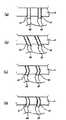
도7은 접속 전극부의 하나의 실시예를 나타낸다. 도7(a)에 나타낸 접속 전극부41은, 접속 전극체4의 두께방향과 평행하게 형성되어 있다. 이러한 경우라도 상기와 같이 접촉자2가 경사져서 배치되어 있는 때에는, 접속 전극부41의 내부측 표면에 접촉자2가 문질러지면서 접촉하게 된다.Fig. 7 shows one embodiment of the connecting electrode portion. The connection electrode
도7(b)는 접속 전극부41이 접속 전극체4의 표면에 대하여 일정 각도로 경사져서 형성되었을 경우를 나타낸다. 이 경우에는, 접촉자2가 접속 전극체4의 표면에 대략 직각방향으로 수용되더라도, 접속 전극부41의 내부측 표면을 문지르면서 접촉하게 된다.Fig. 7 (b) shows a case where the connecting
도7(c)는 접속 전극부41이 '>'자 모양으로 형성되었을 경우를 나타낸다. 이 경우에는, 접촉자2가 도7(b)와 같이 문지르면서 접촉하여 내부에 수용됨과 아울러 접속 전극부41이 '>'자 모양의 정점부에서 역방향의 경사를 형성하고 있으므로, 상기 정점부에서는 확실하게 접촉자2가 내부측 표면과 접촉하게 된다.Fig. 7 (c) shows a case where the connecting
도7(d)는, 접속 전극부41이 만곡하여 형성되었을 경우를 나타낸다. 이 경우에는, 접촉자2가 수용될 때에 상기 접속 전극부41의 내부측 표면을 따라 만곡하여 표면을 문지르면서 접촉하게 된다. 또한 이 경우에는, 도7(c)보다 접촉자2에 영향을 미치는 정도가 낮기 때문에 접촉자2를 넣었다 빼었다 하는 것을 용이하게 할 수 있다.Fig. 7 (d) shows a case where the connecting
도7에서 나타낸 이러한 접속 전극부41의 형상은, 이에 한정되는 것이 아니라 접촉자2의 출입방향에 대하여 접속 전극부41의 수용방향이 교차되도록 형성되게 설정할 수 있다. 이렇게 접속 전극부41을 형성함으로써, 접촉자2가 확실하게 접속 전극부41의 내측표면에 접촉하게 됨과 아울러 수용될 때에 내부측 표면을 문지르면서 수용되므로, 접촉 저항값이 낮은 동시에 접촉 저항값의 안정성이 높은 접촉자2와 접속 전극부41의 접속을 가능하게 한다.The shape of the
또한 다른 구체적인 예로서 도8에 나타나 있는 바와 같이, 접속 전극부41 내부에 수용되는 접촉자2의 선단2A를 접촉자2의 장축에 대하여 굴곡하여 형성한다.As another specific example, as shown in Fig. 8, the
이렇게 접촉자2의 선단2A를 굴곡하여 형성함으로써, 접촉자2의 선단2A가 접속 전극부41에 수용될 때에 접속 전극부41의 내측표면을 문지르면서 접촉하게 된다.By bending the
상기 도8에 나타낸 접촉자2는, 접촉자2의 선단2A가 접촉자2의 중심축으로부터 폭W를 구비하도록 굴곡되어 있다. 상기 폭W는 접속 전극부41의 내경(內徑)과 대략 동일한 정도로 형성되는 것이 바람직하다. 상기 폭W가 접속 전극부41의 내경과 대략 동일하게 형성됨으로써 확실하게 내측표면에 접촉할 수 있을 뿐만 아니라 굴곡되는 양(폭)을 작게 할 수 있기 때문이다.The
도9는 본 발명에 관한 기판검사용 치구를 사용하고 있는 상태를 나 타낸다.Fig. 9 shows a state where the substrate inspection jig according to the present invention is used.
상기 도9에서는, 복수의 접촉자2의 수용부2A가 접속 전극부41 내부에 수용되어 있다. 도9에서는 나타나 있지 않지만, 접촉자2의 수용부2A가 굴곡형상이거나 접촉자2가 경사져서 배치되거나 하는 경우에는, 접속 전극부41 내에 접촉자2가 수용되는 때에 내부측 표면을 문지르면서 접촉하여 수용된다. 또한 도9에서는 편의상 접촉자2가 접속 전극부41의 대략 중앙에 위치하고 있다.In FIG. 9, the
접촉자2가 접속 전극부41에 수용되면, 접촉자 지지체3이나 접속 전극체4를 상대적으로 이동시킴으로써, 접촉자2의 수용부2A를 확실하게 접속 전극부41의 내부측 표면에 압접시키는 것이 바람직하다.When the
접촉자2의 장축에 대하여 직각방향으로 접촉자 지지체3과 접속 전극체4를 이동시킴으로써, 접속 전극부41의 내부측 표면에 확실하게 접촉시키는 것을 나타내고 있다. 이와 같이 접촉자 지지체3 및/또는 접속 전극체4를 접촉자2의 출입방향에 대하여 경사지게 함으로써, 접촉자2의 수용부2A를 접속 전극부41의 내부측 표면에 보다 안정적으로 접촉시키는 것이 가능하게 된다.The
도10은, 접속 전극체가 구비하는 활주부의 하나의 실시예를 나타낸다. 상기 도10에 나타낸 활주부는, 제1판부재43, 제2판부재44와 제4판부재45의 3장으로 구성된 접속 전극체4를 구비하여 이루어진다. 이러한 3장의 판부재를 관통하도록 접속 전극부41이 형성되어 있다. 제1판부재43과 제3판부재45 는 고정부재이고 제2판부재44가 슬라이드 하는 기구로 되어 있다. 이 때문에 도10(b)에 나타나 있는 바와 같이, 제2판부재44가 슬라이드 하여 접속 전극부41을 측면측에서 가압하게 되고, 접속 전극부41이 만곡 형상이 되어 접촉자2의 수용부2A를 측면으로부터 가압하여 접촉하게 된다.Fig. 10 shows one embodiment of the sliding portion provided in the connecting electrode body. The sliding part shown in FIG. 10 is provided with the connecting
상기 도10으로 나타낸 접속 전극체4에서는 3장의 판부재를 사용하여 설명했지만, 3장에 한정되지 않고 더 복수의 판부재를 사용하여 활주부를 형성하여도 무방하다.Although the
또한 도10에서는, 편의상 접촉자2가 접속 전극부41의 구멍방향에 대하여 대략 평행하게 되는 위치에 놓여져 있다.In Fig. 10, for convenience, the
도11은 접속 전극부의 전극 단자를 나타내는 개략적인 구성도이다.Fig. 11 is a schematic configuration diagram showing an electrode terminal of a connecting electrode portion.
도11(a)에 나타낸 접속 전극부41의 전극 단자는 부호 421과 부호 422로 나타나 있다. 상기 전극 단자421, 422는 각각 도선(導線)으로 형성되어 있고 각 도선이 기판검사장치 본체에 접속되어 있다. 이 때문에 접속 전극부41에 2개의 단자가 설치되는 것이 되어 4단자 측정을 할 수 있다.Electrode terminals of the connecting
상기 구성을 사용함으로써, 전극측의 접촉저항은 극히 작고(또는 작거나) 안정한 값이 된다. 이 때문에 검사점 측의 접촉저항만을 고려하면, 검사점에 직접 2개의 단자를 접촉시켰을 경우와 대략 동일한 측정결과를 얻을 수 있게 된다.By using the above configuration, the contact resistance on the electrode side becomes extremely small (or small) and a stable value. For this reason, if only the contact resistance on the inspection point side is taken into account, the measurement result is almost the same as in the case where two terminals are directly in contact with the inspection point.
도11(b)에 나타낸 접속 전극부41의 전극 단자42는 1개의 도선을 사용함으로써 형성되어 있다.The
상기 전극 단자42에서는, 세 갈래 모양의 도전 소재의 일단이 접속 전극부41에 전기적으로 접속되고, 나머지 단자가 2개의 전극 단자421, 422로서 기판검사장치 본체와 전기적으로 접속되어 있다.In the
이러한 구성을 사용하는 경우에는, 접속 전극부41에서 세 갈래 부분까지의 거리d만큼 저항값을 검출해 두고 상기 저항값을 보정함으로써 정확한 측정을 할 수 있다.In such a case, accurate measurement can be performed by detecting the resistance value by the distance d from the
도11에 나타나 있는 바와 같이, 접속 전극부41로부터 2개의 전극 단자를 설치함으로써 4단자 측정을 할 수 있다. 이 경우 보통 피검사점에 대하여 2개의 전극 단자를 사용하여 4단자 측정이 이루어지지만, 본 발명의 전극구조(접속 전극부 구조)라면 접촉자2와 접속 전극부의 접촉저항이 극히 작거나 또는 안정되어 있으므로, 안정된 4단자 측정을 할 수 있게 된다.As shown in FIG. 11, four terminal measurement can be performed by providing two electrode terminals from the
본 발명에 관한 기판검사용 치구의 구성의 설명이다.It is an explanation of the structure of the board | substrate inspection jig which concerns on this invention.
다음에 본 발명의 기판검사용 치구에 접촉자2를 부착하는 경우를 설명한다.Next, the case where the
도12는 접촉자를 부착하는 경우의 공정을 나타낸다.12 shows a process in the case of attaching a contactor.
우선, 제1안내구멍33과 제2안내구멍34가 정합하도록 배치한다. 이 때에 보호부36은 제2안내판32에 접촉시켜 둔다.First, the
도12의 실시예로 나타낸 경우에는, 제1안내구멍33과 제2안내구멍34가 수직방향으로 일렬로 배치되도록 배치한다(도12(a)).In the case of the embodiment of Fig. 12, the
이 경우에 제2안내판32가 상측에 배치되고 제1안내판31이 하측에 배 치되어 있다. 이 배치 위치는 특별하게 한정되는 것은 아니지만 제1안내구멍33으로부터 접촉자2가 빠지는 일이 없기 때문에, 이렇게 배치되는 것이 바람직하다.In this case, the
다음에 접촉자2를 제2안내구멍34로부터 삽입한다(도12(b) 참조).Next, the
이 경우에 상기와 같이 제1안내구멍33은 접촉자2의 절연부23의 지름보다 작게 형성되어 있으므로, 접촉자2가 빠지는 일이 없다.In this case, since the
접촉자2가 삽입되면, 제2안내판32와 보호부36을 동시에 슬라이드 시킨다.When the
이 때에 제2안내판32의 제2안내구멍34에는 접촉자2의 절연부23이 결합하게 된다(도5 참조).At this time, the insulating
즉 접촉자2는, 제2안내판32와 보호부36이 슬라이드 함으로써 만곡하게 되고 접촉자2는 가요성이기 때문에 제1안내구멍33을 형성하는 제1안내판31의 측부와, 제2안내구멍34를 형성하는 제2안내판32의 측부(표면부)와 결합하게 된다.That is, the
이 때에 슬라이드 하는 양은, 상기와 같이 제2안내판32의 외측 판부재 쪽이 크게 슬라이드 하게 된다.At this time, as for the amount of sliding, the outer side plate member side of the
다음에 보호부36을 제2안내판32로부터 돌출시킨다(도12(d) 참조).Next, the
보호부36을 돌출시킴으로써 접촉자2의 단부가 보호된다.The end of the
이렇게 하여 접촉자2를 부착할 수 있고 또한 떼어내는 경우에는 상기의 역의 순서로 한다.In this way, when the
계속하여 본 발명에 관한 기판검사용 치구의 하나의 실시예를 설명한다.Subsequently, one example of the substrate inspection jig according to the present invention will be described.
도13은 본 발명에서 실시되는 기판검사용 치구의 하나의 실시예를 나타내고 있다.Figure 13 shows one embodiment of a substrate inspection jig implemented in the present invention.
상기 하나의 실시예에서 나타낸 접촉자2는, 텅스텐을 소재로 하여 길이30mm, 지름90μm의 막대 모양 부재21을 형성하고 수용부2A의 길이가 2mm가 되도록 절연부23을 형성한다.The
또한 접속 전극부41은 내경95μm, 외경125μm이 되는 도전성의 파이프로서 상기 파이프의 내측표면에 도금처리를 한다.The connecting
상기 도13에서 나타낸 하나의 실시예에서는 접속 전극체4가 제1판자 모양부43, 제2판자 모양부44, 제3판자 모양부45와 제4판자 모양부46으로 형성됨과 아울러 제2판자 모양부44를 가로방향으로 이동시키는 활주부47을 구비하고 있다. 상기 제1판자 모양부43과 제3판자 모양부45는 고정된 부재이고 제4판자 모양부46은 기판검사용 치구1'의 대좌(臺座)로서 사용되고 있다.In the embodiment shown in FIG. 13, the connecting
접속 전극부41은, 제1 내지 제3판자 모양부를 관통하도록 형성되어 있다.The connecting
활주부47은, 제2판자 모양부44를 좌우측으로 이동시킬 수 있다. 상기 활주부47은, 좌우 한 쌍의 나사기구를 구비하여 이루어지고, 좌우의 나사를 조정함으로써 제2판자 모양부44의 위치를 조정할 수 있다.The
또한 도13(a)에서는, 제2안내판32와 보호부36의 사이에 공간이 형성되 어 있는 미사용시의 상태이다.In addition, in Fig. 13A, a space is formed between the
도13(b)는 기판검사용 치구1'를 사용하고 있는 상태를 나타내고 있다. 이 때에 제2안내판32와 보호부36이 접촉함과 아울러 접촉자2의 수용부2A가 접속 전극부41에 수용된다. 그리고 상기 접촉자2의 수용부2A가 접속 전극부41의 내측표면을 문지르면서 접촉한 상태가 되어 도통상태를 확립할 수 있다.Fig. 13B shows a state where the substrate inspection jig 1 'is used. At this time, the
또한 상기 기판검사용 치구1'에서는 활주부47을 좌우에 구비하고 있어서, 접촉자2의 수용부2A가 접속 전극부41에 수용된 후에 나사를 조정함으로써 접속 전극체4의 제2판자 모양부44를 가로방향으로 이동시킨다. 이 때에 접속 전극부41의 제2판자 모양부44 부분은 제2판자 모양부44의 이동에 따라 만곡 상태가 되어 접속 전극부41의 내측표면과 접촉자2가 압접된다.In addition, in the substrate inspection jig 1 ', the
상기 하나의 실시예에서는, 접촉자2도 경사지며 접촉자 지지체3에 지지되고 또한 접속 전극체4가 활주부47을 구비하고 있으므로, 접촉자2가 접속 전극부41의 내측표면을 문지르면서 수용됨과 아울러 안정하게 접촉하여 도통상태를 확립할 수 있다.In the above embodiment, since the
도1은 본 발명에 관한 기판검사용 치구를 사용하는 경우의 개략적인 구성을 나타내고 있다.1 shows a schematic configuration in the case of using a substrate inspection jig according to the present invention.
도2는 본 발명에 관한 기판검사용 치구의 개략적인 구성을 나타내고, 접촉자, 접촉자 지지체와 접속 전극체의 위치 구조를 나타내고 있다.Fig. 2 shows a schematic configuration of a substrate inspection jig according to the present invention and shows the positional structure of a contactor, a contact supporter and a connecting electrode body.
도3은 접촉자의 하나의 실시예를 나타낸다. (a)는 막대 모양 부재, (b)는 막대 모양 부재와 통 모양 부재, (c)는 막대 모양 부재, 통 모양 부재와 절연부를 나타내고 있다.3 illustrates one embodiment of a contact. (a) is a rod-shaped member, (b) is a rod-shaped member and a cylindrical member, (c) has shown the rod-shaped member, a cylindrical member, and an insulation part.
도4는 본 발명에 관한 기판검사용 치구의 검사점 측의 구성을 나타내는 개략적인 단면도이다.4 is a schematic cross-sectional view showing the configuration of an inspection point side of a substrate inspection jig according to the present invention.
도5는 본 발명에 관한 기판검사용 치구의 접속 전극 측의 구성을 나타내는 개략적인 단면도이다.Fig. 5 is a schematic cross-sectional view showing the structure of the connecting electrode side of the substrate inspection jig according to the present invention.
도6은 본 발명에 관한 기판검사용 치구를 사용하고 있는 상태를 나타낸다.Fig. 6 shows a state where the substrate inspection jig according to the present invention is used.
도7은(a)∼(d)는 접속 전극부의 하나의 실시예를 각각 나타낸다.7A to 7D show one embodiment of the connecting electrode portion, respectively.
도8은 접촉자의 다른 실시예를 나타낸다.8 shows another embodiment of a contact.
도9는 본 발명에 관한 기판검사 치구의 사용상태를 나타내는 개략적인 구성도이다.9 is a schematic configuration diagram showing a state of use of the substrate inspection jig according to the present invention.
도10은 본 발명에 관한 접촉자와 접속 전극부의 다른 실시예를 나타내고 있다.10 shows another embodiment of the contactor and the connecting electrode section according to the present invention.
도11은 본 발명에 관한 접촉자와 접촉자 지지체의 또 다른 실시예를 나타내고 있다.11 shows another embodiment of a contactor and a contact support according to the present invention.
도12는 본 발명에 관한 기판검사용 치구의 접촉자를 장착하기 위한 공정을 나타낸다.Fig. 12 shows a process for attaching a contactor of a substrate inspection jig according to the present invention.
도13은 본 발명으로 실시되는 기판검사용 치구의 하나의 실시예를 나타내고 있다.Fig. 13 shows one embodiment of the substrate inspection jig implemented by the present invention.
*도면의 주요부분에 대한 부호의 설명** Description of the symbols for the main parts of the drawings *
1·····기판검사용 치구1 ····· jig for board inspection
1'····기판검사용 치구(다른 실시예)1 '···· Jig for inspection of board (other embodiment)
2·····접촉자2 ...
2A····수용부2A ...
3·····접촉자 지지체3 ····· Contact support
31····제1안내판31 ...
32····제2안내판32 ... 2nd Information Board
4·····접속 전극체4 ... electrode body
41····접속 전극부41 ... connection electrode part
42····전극 단자42 Electrode terminals
Claims (5)
Translated fromKoreanApplications Claiming Priority (2)
| Application Number | Priority Date | Filing Date | Title |
|---|---|---|---|
| JP2007108738 | 2007-04-17 | ||
| JPJP-P-2007-00108738 | 2007-04-17 |
Publications (2)
| Publication Number | Publication Date |
|---|---|
| KR20080093865A KR20080093865A (en) | 2008-10-22 |
| KR100975808B1true KR100975808B1 (en) | 2010-08-13 |
Family
ID=40146625
Family Applications (1)
| Application Number | Title | Priority Date | Filing Date |
|---|---|---|---|
| KR1020080023783AExpired - Fee RelatedKR100975808B1 (en) | 2007-04-17 | 2008-03-14 | PCB inspection jig |
Country Status (3)
| Country | Link |
|---|---|
| JP (1) | JP2008286788A (en) |
| KR (1) | KR100975808B1 (en) |
| TW (1) | TW200848759A (en) |
Cited By (1)
| Publication number | Priority date | Publication date | Assignee | Title |
|---|---|---|---|---|
| KR101656047B1 (en) | 2016-03-23 | 2016-09-09 | 주식회사 나노시스 | Jig for Circuit Board Inspection |
Families Citing this family (12)
| Publication number | Priority date | Publication date | Assignee | Title |
|---|---|---|---|---|
| JP2010276510A (en)* | 2009-05-29 | 2010-12-09 | Nidec-Read Corp | Inspection jig |
| JP5381609B2 (en)* | 2009-10-20 | 2014-01-08 | 日本電産リード株式会社 | Inspection jig and contact |
| JP5428748B2 (en)* | 2009-10-21 | 2014-02-26 | 日本電産リード株式会社 | Inspection jig maintenance method and substrate inspection apparatus |
| JP5514619B2 (en)* | 2009-12-24 | 2014-06-04 | ガーディアンジャパン株式会社 | Wiring inspection jig |
| CN103348255B (en)* | 2011-02-10 | 2015-11-25 | 日本电产理德株式会社 | Check tool |
| JP2013003002A (en)* | 2011-06-17 | 2013-01-07 | Hioki Ee Corp | Probe unit and circuit board inspection device |
| JP5662925B2 (en)* | 2011-12-14 | 2015-02-04 | 富士通株式会社 | Jig identification support device, jig identification support method, and jig identification support program |
| JP6184667B2 (en)* | 2012-07-26 | 2017-08-23 | 日置電機株式会社 | Probe unit, substrate inspection apparatus, and probe unit manufacturing method |
| JP6104724B2 (en)* | 2013-06-12 | 2017-03-29 | 日置電機株式会社 | Probe unit, substrate inspection apparatus, and probe unit manufacturing method |
| KR20170092523A (en)* | 2014-12-04 | 2017-08-11 | 테크노프로브 에스.피.에이. | Testing head comprising vertical probes |
| TW201942581A (en)* | 2018-03-30 | 2019-11-01 | 日商日本電產理德股份有限公司 | Inspection jig, and inspecting device provided with same |
| JP2024154582A (en)* | 2023-04-19 | 2024-10-31 | 株式会社日本マイクロニクス | Manufacturing jig for electrical connection device and manufacturing method for electrical connection device |
Citations (4)
| Publication number | Priority date | Publication date | Assignee | Title |
|---|---|---|---|---|
| JP2000171514A (en) | 1998-12-08 | 2000-06-23 | Delaware Capital Formation Inc | Inspection jig |
| JP2000292437A (en) | 1992-11-09 | 2000-10-20 | Nhk Spring Co Ltd | Conductive contact and conductive contact unit |
| JP2004163228A (en) | 2002-11-12 | 2004-06-10 | Toyo Denshi Giken Kk | Probe and contact device using the same |
| JP2005099037A (en) | 2004-11-17 | 2005-04-14 | Koyo Technos:Kk | Contact pin |
Family Cites Families (2)
| Publication number | Priority date | Publication date | Assignee | Title |
|---|---|---|---|---|
| JP3505495B2 (en)* | 2000-09-13 | 2004-03-08 | 日本電産リード株式会社 | Inspection jig for substrate inspection, substrate inspection device provided with the inspection jig, and method of assembling inspection jig for substrate inspection |
| JP2006329998A (en)* | 2006-07-19 | 2006-12-07 | Nidec-Read Corp | Substrate inspecting tool, and inspection probe used therefor |
- 2008
- 2008-03-14KRKR1020080023783Apatent/KR100975808B1/ennot_activeExpired - Fee Related
- 2008-04-02JPJP2008095972Apatent/JP2008286788A/enactivePending
- 2008-04-15TWTW097113668Apatent/TW200848759A/ennot_activeIP Right Cessation
Patent Citations (4)
| Publication number | Priority date | Publication date | Assignee | Title |
|---|---|---|---|---|
| JP2000292437A (en) | 1992-11-09 | 2000-10-20 | Nhk Spring Co Ltd | Conductive contact and conductive contact unit |
| JP2000171514A (en) | 1998-12-08 | 2000-06-23 | Delaware Capital Formation Inc | Inspection jig |
| JP2004163228A (en) | 2002-11-12 | 2004-06-10 | Toyo Denshi Giken Kk | Probe and contact device using the same |
| JP2005099037A (en) | 2004-11-17 | 2005-04-14 | Koyo Technos:Kk | Contact pin |
Cited By (1)
| Publication number | Priority date | Publication date | Assignee | Title |
|---|---|---|---|---|
| KR101656047B1 (en) | 2016-03-23 | 2016-09-09 | 주식회사 나노시스 | Jig for Circuit Board Inspection |
Also Published As
| Publication number | Publication date |
|---|---|
| TW200848759A (en) | 2008-12-16 |
| KR20080093865A (en) | 2008-10-22 |
| JP2008286788A (en) | 2008-11-27 |
| TWI354108B (en) | 2011-12-11 |
Similar Documents
| Publication | Publication Date | Title |
|---|---|---|
| KR100975808B1 (en) | PCB inspection jig | |
| KR101021744B1 (en) | Substrate inspection jig and electrode structure of connecting electrode in this jig | |
| KR102366546B1 (en) | Electrical Contactor and Electrical Connecting Apparatus | |
| US9733299B2 (en) | Inspection jig | |
| KR20190129927A (en) | Electrical connection device | |
| US6822466B1 (en) | Alignment/retention device for connector-less probe | |
| KR20070005520A (en) | Socket for inspection apparatus | |
| US11372022B2 (en) | Electrical contactor and electrical connecting apparatus | |
| JP5070956B2 (en) | Substrate inspection contact and substrate inspection jig | |
| TWI427297B (en) | Fixture for circuit board inspection | |
| JP2017036997A (en) | Inspection apparatus and inspection method for double-sided circuit board | |
| JP5245279B2 (en) | Substrate inspection jig and electrode structure of connection electrode portion in this jig | |
| JP7393873B2 (en) | Electrical contacts and probe cards | |
| KR100725838B1 (en) | Probe Cards for Wafer Testing | |
| JP2009008516A (en) | Tool and method for substrate inspection | |
| KR20070117452A (en) | Board inspection fixture and board inspection device | |
| KR20210132709A (en) | Electrical Contacts and Electrical Connections | |
| JP2010091314A (en) | Board inspection tool and inspection probe | |
| US20250147073A1 (en) | Probe card and method for design probe card and measuring method and system for detecting device under test using the probe card | |
| JP2007304032A (en) | Substrate inspection fixture and electrode structure of connection electrode part in the fixture | |
| JP2009300391A (en) | Inspection method of electronic board and inspection attachment device used therefor | |
| KR101317251B1 (en) | Probe Card | |
| JP2006294281A (en) | Inspection equipment for semiconductor devices | |
| KR20230151879A (en) | Contact probe | |
| JP2007178311A (en) | Probe |
Legal Events
| Date | Code | Title | Description |
|---|---|---|---|
| A201 | Request for examination | ||
| PA0109 | Patent application | St.27 status event code:A-0-1-A10-A12-nap-PA0109 | |
| PA0201 | Request for examination | St.27 status event code:A-1-2-D10-D11-exm-PA0201 | |
| PG1501 | Laying open of application | St.27 status event code:A-1-1-Q10-Q12-nap-PG1501 | |
| E902 | Notification of reason for refusal | ||
| PE0902 | Notice of grounds for rejection | St.27 status event code:A-1-2-D10-D21-exm-PE0902 | |
| P11-X000 | Amendment of application requested | St.27 status event code:A-2-2-P10-P11-nap-X000 | |
| P13-X000 | Application amended | St.27 status event code:A-2-2-P10-P13-nap-X000 | |
| E701 | Decision to grant or registration of patent right | ||
| PE0701 | Decision of registration | St.27 status event code:A-1-2-D10-D22-exm-PE0701 | |
| GRNT | Written decision to grant | ||
| PR0701 | Registration of establishment | St.27 status event code:A-2-4-F10-F11-exm-PR0701 | |
| PR1002 | Payment of registration fee | St.27 status event code:A-2-2-U10-U11-oth-PR1002 Fee payment year number:1 | |
| PG1601 | Publication of registration | St.27 status event code:A-4-4-Q10-Q13-nap-PG1601 | |
| FPAY | Annual fee payment | Payment date:20130619 Year of fee payment:4 | |
| PR1001 | Payment of annual fee | St.27 status event code:A-4-4-U10-U11-oth-PR1001 Fee payment year number:4 | |
| FPAY | Annual fee payment | Payment date:20140710 Year of fee payment:5 | |
| PR1001 | Payment of annual fee | St.27 status event code:A-4-4-U10-U11-oth-PR1001 Fee payment year number:5 | |
| LAPS | Lapse due to unpaid annual fee | ||
| PC1903 | Unpaid annual fee | St.27 status event code:A-4-4-U10-U13-oth-PC1903 Not in force date:20150810 Payment event data comment text:Termination Category : DEFAULT_OF_REGISTRATION_FEE | |
| PC1903 | Unpaid annual fee | St.27 status event code:N-4-6-H10-H13-oth-PC1903 Ip right cessation event data comment text:Termination Category : DEFAULT_OF_REGISTRATION_FEE Not in force date:20150810 | |
| P22-X000 | Classification modified | St.27 status event code:A-4-4-P10-P22-nap-X000 | |
| R18-X000 | Changes to party contact information recorded | St.27 status event code:A-5-5-R10-R18-oth-X000 |