KR100975797B1 - Semiconductor devices - Google Patents
Semiconductor devicesDownload PDFInfo
- Publication number
- KR100975797B1 KR100975797B1KR1020070130793AKR20070130793AKR100975797B1KR 100975797 B1KR100975797 B1KR 100975797B1KR 1020070130793 AKR1020070130793 AKR 1020070130793AKR 20070130793 AKR20070130793 AKR 20070130793AKR 100975797 B1KR100975797 B1KR 100975797B1
- Authority
- KR
- South Korea
- Prior art keywords
- transistor
- electrode
- current
- electrically connected
- tft
- Prior art date
- Legal status (The legal status is an assumption and is not a legal conclusion. Google has not performed a legal analysis and makes no representation as to the accuracy of the status listed.)
- Expired - Fee Related
Links
Images


Classifications
- H—ELECTRICITY
- H10—SEMICONDUCTOR DEVICES; ELECTRIC SOLID-STATE DEVICES NOT OTHERWISE PROVIDED FOR
- H10D—INORGANIC ELECTRIC SEMICONDUCTOR DEVICES
- H10D84/00—Integrated devices formed in or on semiconductor substrates that comprise only semiconducting layers, e.g. on Si wafers or on GaAs-on-Si wafers
- H10D84/80—Integrated devices formed in or on semiconductor substrates that comprise only semiconducting layers, e.g. on Si wafers or on GaAs-on-Si wafers characterised by the integration of at least one component covered by groups H10D12/00 or H10D30/00, e.g. integration of IGFETs
- H10D84/82—Integrated devices formed in or on semiconductor substrates that comprise only semiconducting layers, e.g. on Si wafers or on GaAs-on-Si wafers characterised by the integration of at least one component covered by groups H10D12/00 or H10D30/00, e.g. integration of IGFETs of only field-effect components
- H10D84/83—Integrated devices formed in or on semiconductor substrates that comprise only semiconducting layers, e.g. on Si wafers or on GaAs-on-Si wafers characterised by the integration of at least one component covered by groups H10D12/00 or H10D30/00, e.g. integration of IGFETs of only field-effect components of only insulated-gate FETs [IGFET]
- G—PHYSICS
- G09—EDUCATION; CRYPTOGRAPHY; DISPLAY; ADVERTISING; SEALS
- G09G—ARRANGEMENTS OR CIRCUITS FOR CONTROL OF INDICATING DEVICES USING STATIC MEANS TO PRESENT VARIABLE INFORMATION
- G09G3/00—Control arrangements or circuits, of interest only in connection with visual indicators other than cathode-ray tubes
- G09G3/20—Control arrangements or circuits, of interest only in connection with visual indicators other than cathode-ray tubes for presentation of an assembly of a number of characters, e.g. a page, by composing the assembly by combination of individual elements arranged in a matrix no fixed position being assigned to or needed to be assigned to the individual characters or partial characters
- G09G3/22—Control arrangements or circuits, of interest only in connection with visual indicators other than cathode-ray tubes for presentation of an assembly of a number of characters, e.g. a page, by composing the assembly by combination of individual elements arranged in a matrix no fixed position being assigned to or needed to be assigned to the individual characters or partial characters using controlled light sources
- G09G3/30—Control arrangements or circuits, of interest only in connection with visual indicators other than cathode-ray tubes for presentation of an assembly of a number of characters, e.g. a page, by composing the assembly by combination of individual elements arranged in a matrix no fixed position being assigned to or needed to be assigned to the individual characters or partial characters using controlled light sources using electroluminescent panels
- G09G3/32—Control arrangements or circuits, of interest only in connection with visual indicators other than cathode-ray tubes for presentation of an assembly of a number of characters, e.g. a page, by composing the assembly by combination of individual elements arranged in a matrix no fixed position being assigned to or needed to be assigned to the individual characters or partial characters using controlled light sources using electroluminescent panels semiconductive, e.g. using light-emitting diodes [LED]
- G09G3/3208—Control arrangements or circuits, of interest only in connection with visual indicators other than cathode-ray tubes for presentation of an assembly of a number of characters, e.g. a page, by composing the assembly by combination of individual elements arranged in a matrix no fixed position being assigned to or needed to be assigned to the individual characters or partial characters using controlled light sources using electroluminescent panels semiconductive, e.g. using light-emitting diodes [LED] organic, e.g. using organic light-emitting diodes [OLED]
- G09G3/3225—Control arrangements or circuits, of interest only in connection with visual indicators other than cathode-ray tubes for presentation of an assembly of a number of characters, e.g. a page, by composing the assembly by combination of individual elements arranged in a matrix no fixed position being assigned to or needed to be assigned to the individual characters or partial characters using controlled light sources using electroluminescent panels semiconductive, e.g. using light-emitting diodes [LED] organic, e.g. using organic light-emitting diodes [OLED] using an active matrix
- G09G3/3233—Control arrangements or circuits, of interest only in connection with visual indicators other than cathode-ray tubes for presentation of an assembly of a number of characters, e.g. a page, by composing the assembly by combination of individual elements arranged in a matrix no fixed position being assigned to or needed to be assigned to the individual characters or partial characters using controlled light sources using electroluminescent panels semiconductive, e.g. using light-emitting diodes [LED] organic, e.g. using organic light-emitting diodes [OLED] using an active matrix with pixel circuitry controlling the current through the light-emitting element
- G09G3/3241—Control arrangements or circuits, of interest only in connection with visual indicators other than cathode-ray tubes for presentation of an assembly of a number of characters, e.g. a page, by composing the assembly by combination of individual elements arranged in a matrix no fixed position being assigned to or needed to be assigned to the individual characters or partial characters using controlled light sources using electroluminescent panels semiconductive, e.g. using light-emitting diodes [LED] organic, e.g. using organic light-emitting diodes [OLED] using an active matrix with pixel circuitry controlling the current through the light-emitting element the current through the light-emitting element being set using a data current provided by the data driver, e.g. by using a two-transistor current mirror
- G—PHYSICS
- G09—EDUCATION; CRYPTOGRAPHY; DISPLAY; ADVERTISING; SEALS
- G09G—ARRANGEMENTS OR CIRCUITS FOR CONTROL OF INDICATING DEVICES USING STATIC MEANS TO PRESENT VARIABLE INFORMATION
- G09G3/00—Control arrangements or circuits, of interest only in connection with visual indicators other than cathode-ray tubes
- G09G3/20—Control arrangements or circuits, of interest only in connection with visual indicators other than cathode-ray tubes for presentation of an assembly of a number of characters, e.g. a page, by composing the assembly by combination of individual elements arranged in a matrix no fixed position being assigned to or needed to be assigned to the individual characters or partial characters
- G09G3/22—Control arrangements or circuits, of interest only in connection with visual indicators other than cathode-ray tubes for presentation of an assembly of a number of characters, e.g. a page, by composing the assembly by combination of individual elements arranged in a matrix no fixed position being assigned to or needed to be assigned to the individual characters or partial characters using controlled light sources
- G09G3/30—Control arrangements or circuits, of interest only in connection with visual indicators other than cathode-ray tubes for presentation of an assembly of a number of characters, e.g. a page, by composing the assembly by combination of individual elements arranged in a matrix no fixed position being assigned to or needed to be assigned to the individual characters or partial characters using controlled light sources using electroluminescent panels
- G09G3/32—Control arrangements or circuits, of interest only in connection with visual indicators other than cathode-ray tubes for presentation of an assembly of a number of characters, e.g. a page, by composing the assembly by combination of individual elements arranged in a matrix no fixed position being assigned to or needed to be assigned to the individual characters or partial characters using controlled light sources using electroluminescent panels semiconductive, e.g. using light-emitting diodes [LED]
- G09G3/3208—Control arrangements or circuits, of interest only in connection with visual indicators other than cathode-ray tubes for presentation of an assembly of a number of characters, e.g. a page, by composing the assembly by combination of individual elements arranged in a matrix no fixed position being assigned to or needed to be assigned to the individual characters or partial characters using controlled light sources using electroluminescent panels semiconductive, e.g. using light-emitting diodes [LED] organic, e.g. using organic light-emitting diodes [OLED]
- G09G3/3275—Details of drivers for data electrodes
- G09G3/3283—Details of drivers for data electrodes in which the data driver supplies a variable data current for setting the current through, or the voltage across, the light-emitting elements
- G—PHYSICS
- G11—INFORMATION STORAGE
- G11C—STATIC STORES
- G11C5/00—Details of stores covered by group G11C11/00
- G11C5/14—Power supply arrangements, e.g. power down, chip selection or deselection, layout of wirings or power grids, or multiple supply levels
- H—ELECTRICITY
- H10—SEMICONDUCTOR DEVICES; ELECTRIC SOLID-STATE DEVICES NOT OTHERWISE PROVIDED FOR
- H10H—INORGANIC LIGHT-EMITTING SEMICONDUCTOR DEVICES HAVING POTENTIAL BARRIERS
- H10H29/00—Integrated devices, or assemblies of multiple devices, comprising at least one light-emitting semiconductor element covered by group H10H20/00
- H10H29/10—Integrated devices comprising at least one light-emitting semiconductor component covered by group H10H20/00
- G—PHYSICS
- G09—EDUCATION; CRYPTOGRAPHY; DISPLAY; ADVERTISING; SEALS
- G09G—ARRANGEMENTS OR CIRCUITS FOR CONTROL OF INDICATING DEVICES USING STATIC MEANS TO PRESENT VARIABLE INFORMATION
- G09G2300/00—Aspects of the constitution of display devices
- G09G2300/04—Structural and physical details of display devices
- G09G2300/0421—Structural details of the set of electrodes
- G09G2300/0426—Layout of electrodes and connections
- G—PHYSICS
- G09—EDUCATION; CRYPTOGRAPHY; DISPLAY; ADVERTISING; SEALS
- G09G—ARRANGEMENTS OR CIRCUITS FOR CONTROL OF INDICATING DEVICES USING STATIC MEANS TO PRESENT VARIABLE INFORMATION
- G09G2300/00—Aspects of the constitution of display devices
- G09G2300/08—Active matrix structure, i.e. with use of active elements, inclusive of non-linear two terminal elements, in the pixels together with light emitting or modulating elements
- G09G2300/0809—Several active elements per pixel in active matrix panels
- G09G2300/0814—Several active elements per pixel in active matrix panels used for selection purposes, e.g. logical AND for partial update
- G—PHYSICS
- G09—EDUCATION; CRYPTOGRAPHY; DISPLAY; ADVERTISING; SEALS
- G09G—ARRANGEMENTS OR CIRCUITS FOR CONTROL OF INDICATING DEVICES USING STATIC MEANS TO PRESENT VARIABLE INFORMATION
- G09G2300/00—Aspects of the constitution of display devices
- G09G2300/08—Active matrix structure, i.e. with use of active elements, inclusive of non-linear two terminal elements, in the pixels together with light emitting or modulating elements
- G09G2300/0809—Several active elements per pixel in active matrix panels
- G09G2300/0842—Several active elements per pixel in active matrix panels forming a memory circuit, e.g. a dynamic memory with one capacitor
- G09G2300/0852—Several active elements per pixel in active matrix panels forming a memory circuit, e.g. a dynamic memory with one capacitor being a dynamic memory with more than one capacitor
- G—PHYSICS
- G09—EDUCATION; CRYPTOGRAPHY; DISPLAY; ADVERTISING; SEALS
- G09G—ARRANGEMENTS OR CIRCUITS FOR CONTROL OF INDICATING DEVICES USING STATIC MEANS TO PRESENT VARIABLE INFORMATION
- G09G2300/00—Aspects of the constitution of display devices
- G09G2300/08—Active matrix structure, i.e. with use of active elements, inclusive of non-linear two terminal elements, in the pixels together with light emitting or modulating elements
- G09G2300/0809—Several active elements per pixel in active matrix panels
- G09G2300/0842—Several active elements per pixel in active matrix panels forming a memory circuit, e.g. a dynamic memory with one capacitor
- G09G2300/0861—Several active elements per pixel in active matrix panels forming a memory circuit, e.g. a dynamic memory with one capacitor with additional control of the display period without amending the charge stored in a pixel memory, e.g. by means of additional select electrodes
- G—PHYSICS
- G09—EDUCATION; CRYPTOGRAPHY; DISPLAY; ADVERTISING; SEALS
- G09G—ARRANGEMENTS OR CIRCUITS FOR CONTROL OF INDICATING DEVICES USING STATIC MEANS TO PRESENT VARIABLE INFORMATION
- G09G2310/00—Command of the display device
- G09G2310/02—Addressing, scanning or driving the display screen or processing steps related thereto
- G09G2310/0243—Details of the generation of driving signals
- G09G2310/0251—Precharge or discharge of pixel before applying new pixel voltage
- G—PHYSICS
- G09—EDUCATION; CRYPTOGRAPHY; DISPLAY; ADVERTISING; SEALS
- G09G—ARRANGEMENTS OR CIRCUITS FOR CONTROL OF INDICATING DEVICES USING STATIC MEANS TO PRESENT VARIABLE INFORMATION
- G09G2320/00—Control of display operating conditions
- G09G2320/02—Improving the quality of display appearance
- G09G2320/0233—Improving the luminance or brightness uniformity across the screen
- G—PHYSICS
- G09—EDUCATION; CRYPTOGRAPHY; DISPLAY; ADVERTISING; SEALS
- G09G—ARRANGEMENTS OR CIRCUITS FOR CONTROL OF INDICATING DEVICES USING STATIC MEANS TO PRESENT VARIABLE INFORMATION
- G09G2320/00—Control of display operating conditions
- G09G2320/02—Improving the quality of display appearance
- G09G2320/0252—Improving the response speed
Landscapes
- Engineering & Computer Science (AREA)
- Physics & Mathematics (AREA)
- Computer Hardware Design (AREA)
- General Physics & Mathematics (AREA)
- Theoretical Computer Science (AREA)
- Power Engineering (AREA)
- Control Of Indicators Other Than Cathode Ray Tubes (AREA)
- Electroluminescent Light Sources (AREA)
- Control Of El Displays (AREA)
- Devices For Indicating Variable Information By Combining Individual Elements (AREA)
Abstract
Translated fromKoreanDescription
Translated fromKorean본 발명은 반도체 디바이스의 구조에 관한 것이다. 구체적으로, 본 발명은 유리 또는 플라스틱과 같은 절연체에 제조되는 박막 트랜지스터(이후, TFT라 칭해짐)를 갖는 액티브 매트릭스 반도체 디바이스의 구조에 관한 것이다. 또한, 본 발명은 디스플레이 부분으로 상기 타입의 반도체 디바이스를 이용하는 전자 장비에 관한 것이다.The present invention relates to a structure of a semiconductor device. Specifically, the present invention relates to the structure of an active matrix semiconductor device having a thin film transistor (hereinafter referred to as TFT) made of an insulator such as glass or plastic. The present invention also relates to electronic equipment using the above type of semiconductor device as the display portion.
최근에 전계 발광(EL) 디스플레이 디바이스들 및 FED(전계 방출 디스플레이들) 등의 자기 발광 디스플레이 디바이스들의 개발이 활발해지고 있다. 자기 발광 디스플레이 디바이스의 이점은, 액정 디스플레이 디바이스(LCD)에 필요한 후광 등을 필요로 하지 않고, 시야각에 거의 제한이 없기 때문에 보다 얇게 제조될 수 있다는 것과, 높은 가시성에 있다.In recent years, the development of self-luminous display devices such as electroluminescent (EL) display devices and field emission displays (FED) has been actively developed. The advantages of self-emissive display devices are that they can be made thinner because they do not require a back light or the like required for a liquid crystal display device (LCD), and there is almost no limitation on the viewing angle, and high visibility.
용어 EL 소자는 전계의 인가에 의해 발생되는 발광이 얻어질 수 있는 발광 층을 가지는 소자를 나타낸다. 단일항 여기 상태(singlet excitation state)(형광)에서 베이스 상태로 되돌아올 때 발광이 발생되고, 발광층의 삼중항 여기 상태(triplet excitation state)(인광)에서 베이스 상태로 되돌아올 때 발광이 발생되며, 본 발명의 반도체 디바이스는 전술된 발광 타입 중 어느 하나를 이용할 수 있다.The term EL element refers to an element having a light emitting layer in which light emission generated by application of an electric field can be obtained. Light emission is generated when returning to the base state from the singlet excitation state (fluorescence), light emission is generated when returning to the base state from the triplet excitation state (phosphorescence) of the light emitting layer, The semiconductor device of the present invention can use any of the above-described light emission types.
EL 소자는 보통은 발광 층이 한 쌍의 전극(애노드와 캐소드) 사이에 배치되는 적층 구조를 가진다. 이스트맨 코닥 컴패니의 탱 등(Tang et al. of Eastman Kodak Company)에 의해 제안되는 "애노드, 정공 수송층, 발광층, 전자 수송층, 캐소드"를 가지는 적층 구조는 통상적인 구조로 제공될 수 있다. 이러한 구조는 발광 효율이 가장 높으며, 현재 연구중인 대부분의 EL 소자들은 이러한 구조를 이용하고 있다.The EL element usually has a laminated structure in which a light emitting layer is disposed between a pair of electrodes (anode and cathode). A laminate structure having "anode, hole transport layer, light emitting layer, electron transport layer, cathode" proposed by Tang et al. Of Eastman Kodak Company may be provided in a conventional structure. This structure has the highest luminous efficiency, and most EL devices currently under study use this structure.
또한, 애노드와 캐소드 사이에 순서대로 적층되는 이하의 층을 갖는 구조들이 존재한다: 정공 주입층, 정공 수송층, 발광층, 전자 수송층; 정공 주입층, 정공 수송층, 발광층, 전자 수송층, 전자 주입층. 전술된 구조 중 임의의 것이 본 발명의 반도체 디바이스에 이용되는 EL 소자 구조로서 이용될 수 있다. 또한, 형광 안료들 등이 발광층에 도핑될 수도 있다.There are also structures having the following layers stacked in order between the anode and the cathode: a hole injection layer, a hole transport layer, a light emitting layer, an electron transport layer; Hole injection layer, hole transport layer, light emitting layer, electron transport layer, electron injection layer. Any of the structures described above can be used as the EL element structure used in the semiconductor device of the present invention. In addition, fluorescent pigments and the like may be doped into the light emitting layer.
애노드와 캐소드 사이의 EL 소자에 형성되는 모든 층들은 본 명세서에서 총칭적으로 "EL 층"으로 칭해진다. 전술된 정공 주입층, 정공 수송층, 발광층, 전자 수송층, 전자 주입층은 모두 EL 층들의 카테고리에 포함되고, 애노드, EL 층, 캐소드로 구성되는 발광 소자는 EL 소자로 칭해진다.All the layers formed in the EL element between the anode and the cathode are collectively referred to herein as an "EL layer". The above-described hole injection layer, hole transport layer, light emitting layer, electron transport layer, and electron injection layer are all included in the category of EL layers, and the light emitting element composed of an anode, an EL layer, and a cathode is called an EL element.
본 발명의 목적은, 신호 라인의 수를 증가시키지 않고도 전술된 여러 문제점을 해결할 수 있는 반도체 디바이스를 제공하는 것이다.It is an object of the present invention to provide a semiconductor device capable of solving the above-mentioned problems without increasing the number of signal lines.
종래의 전류 기입 형태에 의한 문제점 중의 하나는, 신호의 기입 동안의 전류 흐름과 발광 동안의 EL 소자들의 전류 흐름의 크기가 동일하다는 것이다. 즉, 이 문제점을 해결하기 위하여, 기입 신호 동안의 전류 흐름을 발광 동안의 EL 소자의 전류 흐름보다 항상 크게 할 수 있다.One of the problems with the conventional current writing form is that the current flow during the writing of the signal and the magnitude of the current flow of the EL elements during light emission are the same. That is, to solve this problem, the current flow during the write signal can always be made larger than the current flow of the EL element during light emission.
전류들간에 차를 형성하기 위하여, 트랜지스터의 전류 흐름의 크기를 상이하게 한다. 이 실시예에서, 게이트 길이(L)에 주목할 경우, 신호 전류의 기입 동안에 전류가 흐르는 트랜지스터의 게이트 길이(L)는, 발광 동안에 EL 소자에 공급되는 전류가 흐르는 트랜지스터의 게이트 길이(L)보다 짧게 한다. 따라서, 기입은 종래의 EL 소자들의 전류 흐름 보다 많은 전류 흐름을 가짐으로써 실행된다. 따라서, 낮은 그레이 스케일의 경우에 상당한 시간이 요구되는 문제점을 해결할 수 있으며, 또한 잡음의 신호에 대한 영향을 방지할 수 있다.In order to form a difference between the currents, the magnitude of the current flow of the transistors is made different. In this embodiment, when attention is paid to the gate length L, the gate length L of the transistor through which the current flows during the writing of the signal current is shorter than the gate length L of the transistor through which the current supplied to the EL element flows during light emission. do. Thus, writing is performed by having more current flow than that of conventional EL elements. Therefore, it is possible to solve the problem that a considerable time is required in the case of low gray scale, and also to prevent the influence of noise on the signal.
또한, 공통 트랜지스터는, 트랜지스터 특성의 분산이 기입 및 발광 동안에 서로 다른 트랜지스터가 이용되는 구조를 이용할 때와 비교하여 휘도에 영향을 미치지 못하도록, 기입 및 발광 동안에 일부의 트랜지스터에 이용된다.In addition, common transistors are used in some transistors during writing and light emission so that dispersion of transistor characteristics does not affect luminance as compared to when using a structure in which different transistors are used during writing and light emission.
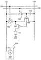
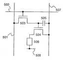
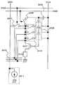
통상적인 반도체 디바이스의 픽셀 구조는 도 5에 도시되고 있다. EL 디스플 레이 디바이스가 통상적인 반도체 디바이스의 일례로서 이용되고 있다. 도 5에 도시된 픽셀은 소스 신호 라인(501), 게이트 신호 라인(502), 스위칭 TFT(503), 구동 TFT(504), 저장 커패시터(505), EL 소자(506), 전원(507, 508)를 구비한다.The pixel structure of a typical semiconductor device is shown in FIG. An EL display device is used as an example of a conventional semiconductor device. The pixel shown in Fig. 5 includes a
각 부분 사이의 접속 관계를 설명한다. TFT는 3개의 단자, 게이트, 소스 및 드레인을 가지지만, 여기에서 TFT 구조로 인해 소스 및 드레인을 분명하게 구별짓기가 어렵다. 따라서, 소자들 사이의 접속에 관한 설명은, 제 1 전극으로 칭해지는 한 전극과 소스 또는 드레인과 제 2 전극으로 칭해지는 나머지 전극으로 제공된다. 그러나, TFT들의 온 및 오프에 관한 설명, 각 단자의 전위 등에 관하여 설명할 때, 용어 소스, 드레인 등이 이용된다.The connection relationship between each part is demonstrated. The TFT has three terminals, a gate, a source and a drain, but because of the TFT structure, it is difficult to clearly distinguish between the source and the drain. Thus, a description of the connection between the elements is provided for one electrode called the first electrode and the other electrode called the source or drain and the second electrode. However, when describing the on and off of the TFTs, the potential of each terminal, and the like, the terms source, drain, and the like are used.
스위칭 TFT(503)의 게이트 전극은 게이트 신호 라인(502)에 접속되고, 스위칭 TFT(503)의 제 1 전극은 소스 신호 라인(501)에 접속된다. 스위칭 TFT(503)의 제 2 전극은 구동 TFT(504)의 게이트 전극에 접속된다. 구동 TFT(504)의 제 1 전극은 전원(507)에 접속되고, 구동 TFT(504)의 제 2 전극은 EL 소자(506)의 한 전극에 접속된다. EL 소자(506)의 나머지 전극은 전원(508)에 접속된다. 저장 커패시터(505)는 게이트 전극과 구동 TFT(504)의 제 1 전극 사이에 접속되고, 구동 TFT(504)의 소스와 게이트 사이의 전압을 저장한다.The gate electrode of the switching
게이트 신호 라인(502)의 전위가 변화하여 스위칭 TFT(503)가 턴온되는 경우, 소스 신호 라인(501)에 입력되는 이미지 신호는 구동 TFT(504)의 게이트 전극에 입력된다. 구동 TFT(504)의 게이트와 소스 사이의 전압, 구동 TFT(504)의 소스와 드레인 사이에 흐르는 전류(이후 드레인 전류로 칭해짐)의 양은 입력 이미지 신 호의 전위에 따라 결정된다. 그 전류는 발광하는 EL 소자(506)에 공급된다.When the potential of the
폴리실리콘(이후 P-Si로 칭해짐)을 이용하여 형성되는 TFT들은 단결정 실리콘(이후, A-Si로 칭해짐)을 이용하여 형성되는 TFT들 보다 더 높은 전계 이동도 및 더 많은 통과 전류(on current)를 가지기 때문에, 반도체 디바이스들에 이용되는 트랜지스터들로서 적절하다.TFTs formed using polysilicon (hereinafter referred to as P-Si) have higher field mobility and more pass current (on) than TFTs formed using single crystal silicon (hereinafter referred to as A-Si). It is suitable as transistors used in semiconductor devices.
반대로, 폴리실리콘으로 형성되는 TFT들은 결정 그레인 경계들의 결합으로 인해 전기 특성들의 분산이 쉽게 발생한다는 점에서 문제가 있다.In contrast, TFTs formed of polysilicon have a problem in that dispersion of electrical properties easily occurs due to the combination of crystal grain boundaries.
TFT 구조 픽셀들이 도 5에 도시된 것과 동일한 경우 통과 전류와 TFT 문턱값 등의 특성에 있어서 픽셀마다 분산이 발생하고, 동일 이미지 신호가 입력되는 경우에도 입력 이미지 신호에 응답하여 TFT의 드레인 전류의 양에 큰 차이가 있으며, 따라서 EL 소자들(506)의 휘도가 분산된다.In the case where the TFT structure pixels are the same as those shown in Fig. 5, the dispersion occurs per pixel in characteristics such as the pass current and the TFT threshold value, and the amount of drain current of the TFT in response to the input image signal even when the same image signal is input. There is a large difference in, and therefore the luminance of the
이러한 형태의 문제점을 해결하기 위하여, 소망의 전류 양은 TFT 특성들에 상관없이 EL 소자들에 공급될 수 있다. 따라서, TFT 특성들에 영향을 받지 않고도 EL 소자들에 흐르는 전류의 크기를 제어할 수 있는 다양한 형태의 전류 기입(write-in) 픽셀들이 제안되고 있다.In order to solve this type of problem, the desired amount of current can be supplied to the EL elements irrespective of the TFT characteristics. Therefore, various types of current write-in pixels have been proposed that can control the magnitude of the current flowing through the EL elements without being affected by the TFT characteristics.
용어 전류 기입은, 아날로그 또는 디지털 전압 정보에 의한 정상 입력에 대립하는 것으로, 소스 신호 라인들을 이용하여 픽셀들에 입력되는 이미지 신호가 전류에 의해 입력되는 방법을 의미한다. EL 소자들에 공급되는 전류값은 외부의 신호 전류에 의해 설정되고, 동일한 전류는 픽셀들에 흐르게 된다. 이것은 TFT 특성들의 분산에 의해 어떠한 영향도 받지 않는다고 하는 이점을 가진다.The term current writing, as opposed to normal input by analog or digital voltage information, refers to a method in which an image signal input to pixels using source signal lines is input by current. The current value supplied to the EL elements is set by an external signal current, and the same current flows through the pixels. This has the advantage that it is not affected by the dispersion of the TFT characteristics.
통상적인 전류 기입 픽셀들이 몇 가지 일례가 이하에 도시되고, 그 구조, 동작 및 특성들에 관하여 설명이 부여된다.Some examples of conventional current write pixels are shown below, and explanation is given with respect to the structure, operation, and characteristics thereof.
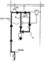
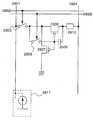
제 1 구조의 일례는 도 6에 도시된다. 도 6의 픽셀은 소스 신호 라인(601), 제 1 내지 제 3 게이트 신호 라인(602~604), 전류 공급 라인(605), TFT들(606~609), 저장 커패시터(610), EL 소자(611) 및 신호 전류 입력 전류 소스(612)를 구비한다.An example of the first structure is shown in FIG. The pixel of FIG. 6 includes a
TFT(606)의 게이트 전극은 제 1 게이트 신호 라인(602)에 접속되고, TFT(606)의 제 1 전극은 소스 신호 라인(601)에 접속되고, TFT(606)의 제 2 전극은 TFT(607)의 제 1 전극, TFT(608)의 제 1 전극 및 TFT(609)의 제 1 전극에 접속된다. TFT(607)의 게이트 전극은 제 2 게이트 신호 라인(603)에 접속되고, TFT(607)의 제 2 전극은 TFT(608)의 게이트 전극에 접속된다. TFT(608)의 제 2 전극은 전류 공급 라인(605)에 접속된다. TFT(609)의 게이트 전극은 제 3 게이트 신호 라인(604)에 접속되고, TFT(609)의 제 2 전극은 EL 소자(611)의 애노드에 접속된다. 저장 커패시터(610)는 TFT(608)의 게이트 전극과 입력 전극 사이에 접속되어, TFT(608)의 게이트와 소스 사이의 전압을 저장한다. 미리 결정된 전위는 전류 공급 라인(605)과 EL 소자(611)의 캐소드에 입력되며, 양자는 상호 전위 차를 가진다.The gate electrode of the
신호 전류의 기입에서 발광까지의 동작은 도 7a 내지 도 7e를 이용하여 설명된다. 각 부분을 나타내는 이 도면들 내에서 이용되는 참조 부호는 도 6의 참조 부호에 기초한다. 도 7a 내지 도 7c는 전류 흐름을 개략적으로 도시하고 있다. 도 7d는 신호 전류의 기입 동안에 각 경로에 흐르는 전류들 사이의 관계를 도시하고, 도 7e는 신호 전류의 동일 기입 동안에 저장 커패시터(610)에 저장되는 전압, 즉 TFT(608)의 게이트와 소스 사이의 전압을 도시한다.The operation from writing of signal current to light emission is explained using Figs. 7A to 7E. Reference numerals used in these figures showing respective parts are based on the reference numerals in FIG. 6. 7A-7C schematically depict the current flow. FIG. 7D shows the relationship between the currents flowing in each path during the writing of the signal current, and FIG. 7E shows the voltage stored in the
처음에, 펄스들은 제 1 게이트 신호 라인(602) 및 제 2 게이트 신호 라인(603)에 입력되며, TFT들(606, 607)은 턴온된다. 이 때, 소스 신호 라인에 흐르는 전류, 즉 신호 전류는 Idata로 간주된다.Initially, pulses are input to the first
전류 Idata는 소스 신호 라인에 흐르기 때문에, 픽셀내의 전류 경로는 도 7a에 도시된 바와 같이 I1과 I2로 나누어진다. 이 두 전류의 관계식은 도 7d에 도시된다. Idata=I1+ I2이다.Since the current Idata flows in the source signal line, the current path in the pixel is divided into I1 and I2 as shown in FIG. 7A. The relationship between these two currents is shown in Figure 7d. Idata = I1 + I2 to be.
전하는 TFT(606)이 턴온되는 순간에 저장 커패시터(610)에 아직 저장되지 않기 때문에, TFT(608)는 턴오프된다. 결국, I2=0, Idata=I1가 된다. 즉, 전류는 상기 기간에는 저장 커패시터(610)의 전하의 저장에 의해서만 흐르게 된다.The charge is not yet stored in the
전하는 저장 커패시터(610)에 점차 저장되고, 전위차는 양 전극 사이에서 발생하기 시작한다(도 7e 참조). TFT(608)는 양 전극 사이의 전위차가 Vth(도 7e에서 점 A)에 도달할 때 턴온되며, 이것에 의해 I2가 발생한다. 전술된 바와 같이, Idata=I1+I2가 되며, 이것에 의해 I1은 점차 감소된다. 전류는 여전히 흐르게 되고, 또한 전하는 저장 커패시터에 저장된다.Electric charge is gradually stored in the
전하는 저장 커패시터(610)의 양 전극의 전위차, 즉 TFT(608)의 게이트와 소스 사이의 전압이 소망의 전압이 될 때까지, 즉 TFT(608)에 전류 Idata가 흐를 수 있게 하는 전압(VGS)이 될 때까지 저장 커패시터(610)에 계속해서 저장된다. 전하의 저장이 완료될 때(도 7e의 점 B), 전류 I2는 흐름을 정지하고, 또 이 때 VGS에 대응하는 전류가 TFT(608)에 흐르게 되고, Idata=I2가 된다(도 7b 참조). 신호 기입 동작들이 따라서 완료된다. 제 1 게이트 신호 라인(602) 및 제 2 게이트 신호 라인(603)의 선택이 최종적으로 완료되고, TFT들(606, 607)은 턴오프된다.The charge is a voltage (VGS) that allows the current Idata to flow through the
발광 동작들은 다음에 다룬다. 펄스는 제 3 게이트 신호 라인(604)에 입력되고, TFT(609)는 턴온된다. 이전에 기입된 VGS는 저장 커패시터(610)에 저장되고, 따라서 TFT(608)는 턴온되고, 전류 Idata는 전류 공급 라인(605)으로부터 흐르게 된다. 이것에 의해, EL 소자(611)는 발광한다. TFT(608)가 이 때 포화 영역에서 동작되는 경우, Idata는 TFT(608)의 소스와 드레인 사이의 전압이 변화되는 경우에도 변화없이 계속해서 흐를 수 있다.Light emission operations are discussed next. The pulse is input to the third
도 17은 제 2 구조의 일례를 도시하고 있다. 도 17의 픽셀은 소스 신호 라인(1701), 제 1 내지 제 3 게이트 신호 라인(1702~1704), 전류 공급 라인(1705), TFT들(1706~1709), 저장 커패시터(1710), EL 소자(1711), 신호 전류를 입력하기 위한 전류 소스(1712)를 구비한다.17 shows an example of the second structure. The pixel of FIG. 17 includes a
TFT(1706)의 게이트 전극은 제 1 게이트 신호 라인(1702)에 접속되고, TFT(1706)의 제 1 전극은 소스 신호 라인(1701)에 접속되고, TFT(1706)의 제 2 전극은 TFT(1708)의 제 1 전극 및 TFT(1709)의 제 1 전극에 접속된다. TFT(1708)의 게이트 전극은 제 2 게이트 신호 라인(1703)에 접속되고, TFT(1708)의 제 2 전극은 전류 공급 라인(1705)에 접속된다. TFT(1707)의 게이트 전극은 제 3 게이트 신호 라인(1704)에 접속되고, TFT(1707)의 제 1 전극은 TFT(1709)의 게이트 전극에 접속되고, TFT(1707)의 제 2 전극은 TFT(1709)의 제 2 전극 및 EL 소자(1711)의 한 전극에 접속된다. 저장 커패시터(1710)는 TFT(1709)의 게이트 전극과 제 1 전극 사이에 접속되고, TFT(1709)의 게이트와 소스 사이의 전압을 저장한다. 미리 결정된 전위들은 전류 공급 라인(1705) 및 EL 소자(1711)의 다른 전극에 입력되어, 상호 전위차를 가지게 된다.The gate electrode of the
발광을 통한 신호 전류의 기입으로부터의 동작은 도 18a 내지 도 18e를 이용하여 설명된다. 각 부분을 나타내는 도면 내에 이용되는 참조 부호들은 도 17의 참조 부호에 기초한다. 도 18a 내지 도 18c는 전류 흐름을 개략적으로 도시하고 있다. 도 18d는 신호 전류의 기입 동안의 각 경로에 흐르는 전류 사이의 관계를 도시하고, 도 18e는 신호 전류의 동일 기입 동안의 저장 커패시터(1710)에 저장되는 전압, 즉 TFT(1709)의 게이트와 소스 사이의 전압을 도시하고 있다.Operation from writing of the signal current through light emission is described using Figs. 18A to 18E. Reference numerals used in the drawings showing respective parts are based on the reference numerals in FIG. 17. 18A-18C schematically illustrate the current flow. 18D shows the relationship between the current flowing in each path during the writing of the signal current, and FIG. 18E shows the voltage stored in the
처음에, 펄스들은 제 1 게이트 신호 라인(1702) 및 제 3 게이트 신호 라인(1704)에 입력되고, TFT(1706, 1707)는 턴온된다. 이 때, 소스 신호 라인(1701)에 흐르는 전류, 즉 신호 전류는 Idata로 간주된다.Initially, pulses are input to the first
전류 Idata는 소스 신호 라인(1701)에 흐르게 되어, 픽셀 내의 전류 경로는 도 18a에 도시된 바와 같이 I1, I2로 나누어진다. 두 전류 사이의 관계는 도 18D에 도시된다. Idata=I1+I2가 된다.The current Idata flows in the
전하는 TFT(1706)이 턴온되는 순간에 저장 커패시터(1710)에 아직 저장되지 않기 때문에, TFT(1709)는 턴오프된다. 결국, I2=0, Idata=I1가 된다. 즉, 전류는 상기 기간에는 저장 커패시터(1710)의 전하의 저장에 의해서만 흐르게 된다.Since electric charge has not yet been stored in the
전하는 저장 커패시터(1710)에 점차 저장되고, 전위차는 양 전극 사이에서 발생하기 시작한다(도 18e 참조). TFT(1709)는 양 전극 사이의 전위차가 Vth(도 18e에서 점 A)에 도달할 때 턴온되어, I2가 발생한다. 전술된 바와 같이, Idata=I1+I2가 되어, I1는 점차 감소된다. 전류는 여전히 흐르게 되고, 또한 전하는 저장 커패시터에 저장된다.Electric charge is gradually stored in the
전하는 저장 커패시터(1710)의 양 전극의 전위차, 즉 TFT(1709)의 게이트와 소스 사이의 전압이 소망의 전압이 될 때까지, 즉 TFT(1709)에 전류 Idata가 흐를 수 있게 하는 전압(VGS)이 될 때까지 저장 커패시터(1710)에 계속해서 저장된다. 전하의 저장이 완료될 때(도 18e의 점 B), 전류 I1은 흐름을 정지하고, 또 이 때 VGS에 대응하는 전류가 TFT(1709)에 흐르게 되고, Idata=I2가 된다(도 18b 참조). 신호 기입 동작들이 따라서 완료된다. 제 1 게이트 신호 라인(1702) 및 제 3 게이트 신호 라인(1704)의 선택이 최종적으로 완료되고, TFT들(1706, 1707)은 턴오프된다.The charge (VGS) allows the current Idata to flow through the
펄스는 제 2 게이트 신호 라인(1703)에 입력되고, TFT(1708)는 턴온된다. 이 때, 이전에 기입된 VGS는 저장 커패시터(1710)에 저장되고, 따라서 TFT(1709)는 턴온되고, 전류 Idata는 전류 공급 라인(1705)으로부터 흐르게 된다. 이것에 의해, EL 소자(1711)는 발광한다. TFT(1709)가 이 때 포화 영역에서 동작되는 경우, Idata는 TFT(1709)의 소스와 드레인 사이의 전압이 변화되는 경우에도 변화없이 계속해서 흐를 수 있게 된다.The pulse is input to the second
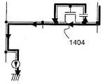
도 19는 제 3 구조의 일례를 도시하고 있다. 도 19의 픽셀은 소스 신호 라인(1901), 제 1 및 제 2 게이트 신호 라인(1902, 1903), 전류 공급 라인(1904), TFT들(1905~1908), 저장 커패시터(1909), EL 소자(1910), 신호 전류를 입력하기 위한 전류 소스(1911)를 구비한다.19 shows an example of the third structure. The pixel of Fig. 19 includes
TFT(1905)의 게이트 전극은 제 1 게이트 신호 라인(1902)에 접속되고, TFT(1905)의 제 1 전극은 소스 신호 라인(1901)에 접속되고, TFT(1906)의 제 2 전극은 TFT(1906)의 제 1 전극 및 TFT(1907)의 제 1 전극에 접속된다. TFT(1906)의 게이트 전극은 제 2 게이트 신호 라인(1903)에 접속되고, TFT(1906)의 제 2 전극은 전류 공급 라인(1907)의 게이트 전극 및 TFT(1908)의 게이트 전극에 접속된다. TFT(1907)의 제 2 전극 및 TFT(1908)의 제 1 전극은 모두 전류 공급 라인(1904)에 접속되고, TFT(1908)의 제 2 전극은 EL 소자(1910)의 애노드에 접속된다. 저장 커패시터(1909)는 TFT들(1907, 1908)의 게이트 전극 사이에 접속되고, TFT(1907)의 제 2 전극과 TFT(1908)의 제 1 전극 사이에 접속된다. 저장 커패시터(1909)는 TFT(1907)의 게이트와 소스 사이의 전압 및 TFT(1908)의 게이트와 소스 사이의 전압을 저장한다. 미리 결정된 전위는 전류 공급 라인(1904) 및 EL 소자(1910)의 캐소드에 입력되어, 상호 전위차를 가지게 된다.The gate electrode of the
발광을 통한 신호 전류의 기입으로부터의 동작은 도 20a 내지 도 20e를 이용하여 설명된다. 각 부분을 나타내는 도면 내에 이용되는 참조 부호는 도 19의 참 조 부호에 기초한다. 도 20a 내지 도 20c는 전류 흐름을 개략적으로 도시하고 있다. 도 20d는 신호 전류의 기입 동안의 각 경로에 흐르는 전류 사이의 관계를 도시하고, 도 20e는 신호 전류의 동일 기입 동안의 저장 커패시터(1909)에 저장되는 전압, 즉 TFT들(1907, 1908)의 게이트와 소스 사이의 전압을 도시하고 있다.The operation from writing of the signal current through light emission is explained using Figs. 20A to 20E. Reference numerals used in the drawings showing respective parts are based on reference numerals in FIG. 20A-20C schematically depict current flow. FIG. 20D shows the relationship between the currents flowing in each path during the writing of the signal current, and FIG. 20E shows the voltages stored in the
처음에, 펄스는 제 1 게이트 신호 라인(1902) 및 제 2 게이트 신호 라인(1903)에 입력되고, TFT들(1905, 1906)은 턴온된다. 이 때, 소스 신호 라인(1901)에 흐르는 전류, 즉 신호 전류는 Idata로 간주된다.Initially, a pulse is input to the first
전류 Idata는 소스 신호 라인(1901)에 흐르게 되어, 픽셀 내의 전류 경로는 도 20a에 도시된 바와 같이 I1, I2로 나누어진다. 두 전류 사이의 관계는 도 20d에 도시된다. Idata=I1+I2가 된다.The current Idata flows in the
전하는 TFT(1905)가 턴온되는 순간에 저장 커패시터(1909)에 아직 저장되지 않기 때문에, TFT들(1907, 1908)은 턴오프된다. 결국, I2=0, Idata=I1가 된다. 즉, 전류는 상기 기간에는 저장 커패시터(1909)의 전하의 저장에 의해서만 흐르게 된다.Since the charge is not yet stored in the
전하는 저장 커패시터(1909)에 점차 저장되고, 전위차는 양 전극 사이에서 발생하기 시작한다(도 20e 참조). TFT(1907)는 양 전극 사이의 전위차가 Vth(도 20e에서 점 A)에 도달할 때 턴온되고, I2가 발생한다. 전술된 바와 같이, Idata=I1+I2가 되어, I1은 점차 감소된다. 전류는 여전히 흐르게 되고, 또한 전하는 저장 커패시터에 저장된다.Electric charge is gradually stored in the
여기서, TFT(1907)는 턴온되고, 또 TFT(1908)도 턴온되며, 전류가 흐르기 시작한다. 그러나, 이 전류는 도 20a에 도시된 바와 같이 독립 경로에 흐르게 되고, 따라서 Idata의 값은 변화하지 않게 되고, 또 I1및 I2에 영향을 미치지 않는다.Here, the
전하는 저장 커패시터(1909)의 양 전극의 전위차, 즉 TFT들(1907, 1908)의 게이트와 소스 사이의 전압이 소망의 전압이 될 때까지, 즉 TFT(1907)에 전류 Idata가 흐를 수 있게 하는 전압(VGS)이 될 때까지 저장 커패시터(1909)에 계속해서 저장된다. 전하의 저장이 완료될 때(도 20e의 점 B), 전류 I1은 흐름을 정지하고, 또 이 때 VGS에 대응하는 전류가 TFT(1907)에 흐르게 되고, Idata=I2가 된다(도 20b 참조). 신호 기입 동작들이 따라서 완료된다. 제 1 게이트 신호 라인(1902) 및 제 2 게이트 신호 라인(1903)의 선택이 최종적으로 완료되고, TFT들(1905, 1906)은 턴오프된다.The charge causes current Idata to flow through the
전하는 TFT(1907)의 전류 Idata의 흐름에 의해 게이트와 소스 사이에 가능한 만큼의 전압이 부여될 때에 저장 커패시터(1909)에 저장된다. TFT들(1907, 1908)은 전류 미러를 형성하며, 이에 따라 상기 전압은 또한 TFT(1908)에 부여되고, TFT(1908)에 전류가 흐르게 된다. 이 전류는 도 20a 내지 도 20e에서 참조 부호 IEL로 표시된다.Electric charge is stored in the
TFT들(1907, 1908)의 게이트 길이 및 채널 폭이 동일한 경우에는, IEL=Idata가 된다. 즉, 신호 전류 Idata와 EL에 흐르는 전류 IEL 사이의 관계는 전류 미러를 구성하는 TFT들(1907, 1908)의 크기를 결정하는 방법에 의해 결정될 수 있다.When the gate length and the channel width of the
상기 일례에서 도시되는 전류 기입의 장점은, TFT들(608)의 특성 등이 분산되는 경우에도 전류 Idata를 흐르게 하는데 필요한 게이트와 소스간이 전압이 저장 커패시터(610)에 저장되는 것이다. 따라서, 소망의 전류는 EL 소자에 정확하게 공급될 수 있으며, 결국 TFT 특성의 분산에 의해 야기되는 휘도 분산을 제어할 수 있게 된다.An advantage of the current write shown in the above example is that the voltage between the gate and the source necessary to flow the current Idata even when the characteristics of the
각 구조의 특성은 표 1에 나타낸다.The characteristics of each structure are shown in Table 1.

우선, 신호 전류 Idata와 EL 소자에 흐르는 전류 IEL 사이의 관계를 살펴보자. 그레이 스케일은 아날로그 그레이 스케일 방법을 이용하는 반도체 디바이스들의 전류의 값으로 표시되며, 따라서 높은 그레이 스케일에 대해서는 대량의 전류가 흐르고, 낮은 그레이 스케일에 대해서는 적은 양의 전류가 흐른다. 즉, 기입 신호 전류의 크기는 그레이 스케일에 따라 상이하다. 이 경우에, 낮은 그레이 스케일 신호를 픽셀에 기입하는데에는 높은 그레이 스케일 신호를 픽셀들에 기입하는 것보다 더 오랜 시간이 요구된다. 또한, 전류는 낮은 그레이 스케일 신호에 대해서는 작고, 따라서 잡음에 매우 쉽게 영향을 받는다.First, let's look at the relationship between the signal current Idata and the current IEL flowing in the EL element. The gray scale is expressed as the value of the current of semiconductor devices using the analog gray scale method, so that a large amount of current flows for the high gray scale, and a small amount of current flows for the low gray scale. That is, the magnitude of the write signal current differs depending on the gray scale. In this case, writing a low gray scale signal to a pixel takes longer than writing a high gray scale signal to the pixels. In addition, the current is small for low gray scale signals and is therefore very easily affected by noise.
다음, 전류-전압 변환 TFT와 구동 TFT 사이의 관계를 살펴보자. 전류-전압 변환 TFT는 소스 신호 라인으로부터 입력되는 신호 전류를 전압 신호로 변환하는데 이용되는 TFT이고, 구동 TFT는 저장 커패시터에 저장된 전압에 따라 전류를 흐르게 하는 TFT이다. 각 구조에 대한 전류-전압 변환 TFT(변환 TFT로 표시됨) 및 구동 TFT의 도면 번호는 표 1에 표시된다.Next, let's look at the relationship between the current-voltage conversion TFT and the driving TFT. The current-voltage converting TFT is a TFT used for converting a signal current input from a source signal line into a voltage signal, and the driving TFT is a TFT which allows current to flow in accordance with the voltage stored in the storage capacitor. The reference numbers of the current-voltage conversion TFTs (indicated by the conversion TFTs) and the driving TFTs for each structure are shown in Table 1.
변환 TFT 및 구동 TFT는 공통이다라는 것은 기입 및 발광 동작에 공통 TFT가 이용되는 것을 의미한다. TFT 분산으로 인한 영향은 따라서 작다. 한편, 제 3 구조에 도시된 바와 같이 변환 TFT 및 구동 TFT가 서로 다른 경우에는, 픽셀 내의 특성 분산에 의한 영향이 있다.The conversion TFT and the driving TFT are common means that the common TFT is used for writing and light emitting operations. The influence due to TFT dispersion is therefore small. On the other hand, when the conversion TFT and the driving TFT are different from each other as shown in the third structure, there is an influence due to the dispersion of characteristics in the pixels.
다음은 신호 전류 경로에 대해서 살펴보자. 신호 전류는 제 1 구조 및 제 3 구조에서 전류 소스에서 전류 공급 라인으로 흐르거나, 또는 전류 공급 라인에서 전류 소스로 흐른다. 한편, 신호 전류는 신호 전류가 제 2 구조를 이용할 경우 기입될 때 전류 소스로부터 EL 소자를 통해 흐른다. EL 소자 자체는, 낮은 그레이 스케일 신호의 기입 이후 높은 그레이 스케일 신호가 기입되는 경우와, 반대 동작이 실행되는 경우에 대해서 상기 타입의 구조를 갖는 부하가 되고, 따라서 기입 시간을 길게 하는 것이 필요하게 된다.Next, let's look at the signal current path. The signal current flows from the current source to the current supply line in the first and third structures, or from the current supply line to the current source. On the other hand, the signal current flows from the current source through the EL element when the signal current is written when using the second structure. The EL element itself becomes a load having the above-described structure for the case where the high gray scale signal is written after the writing of the low gray scale signal and for the case where the reverse operation is executed, and thus it is necessary to lengthen the write time. .
또한, 픽셀 제어는 제 1 및 제 2 구조에 있어서 픽셀의 로우 마다 3개의 게이트 신호 라인을 이용함으로써 실행되며, 이것에 의해 개구비는 종래의 반도체 디바이스에 비해 상당히 감소된다.In addition, pixel control is performed by using three gate signal lines per row of pixels in the first and second structures, whereby the aperture ratio is significantly reduced compared to conventional semiconductor devices.
기입 시간은 낮은 그레이 스케일에 대해서도 대량 전류를 이용하여 기입 동작을 실행함으로써 본 발명에 따라 빨라 질 수 있다. 또한, 변환 TFT들은 신호 기입 동안에 이용되고, 변환 TFT들은 발광 소자에 전류를 공급하기 위해 발광 동안에 구동 TFT들에 부가하여 이용되며, 이것에 의해 기입 및 발광 동안의 TFT들의 특성 분산의 영향은 감소될 수 있다. 또한, 1개 또는 2개의 게이트 신호 라인은 1개 로우의 픽셀을 구동하는데 요구되며, 따라서 통상적인 종래의 전류 기입 픽셀에 비해 높은 개구비가 달성될 수 있다.The write time can be faster in accordance with the present invention by performing a write operation using a large current even for a low gray scale. Further, conversion TFTs are used during signal writing, and conversion TFTs are used in addition to the driving TFTs during light emission to supply current to the light emitting element, whereby the influence of the characteristic dispersion of the TFTs during writing and light emission can be reduced. Can be. In addition, one or two gate signal lines are required to drive one row of pixels, so that a high aperture ratio can be achieved as compared to conventional conventional current write pixels.
본 발명의 구성은 이하에서 기술한다.The configuration of the present invention is described below.
본 발명의 반도체 디바이스는,The semiconductor device of the present invention,
입력 신호 전류를 전압으로 변환하고, 상기 변환된 전압에 대응하는 전류를 전원에서 부하로 공급하는 제 1 수단,First means for converting an input signal current into a voltage and supplying a current corresponding to the converted voltage from a power supply to a load,
상기 변환된 전압을 저장하는 제 2 수단,Second means for storing the converted voltage,
상기 제 2 수단에서 상기 전압을 저장 또는 해방(release)하도록 선택하는 제 3 수단, 및Third means for selecting at the second means to store or release the voltage, and
신호 전류를 입력하는 기간에는 상기 전원에서 상기 부하로 상기 전류 공급을 차단하고, 상기 부하를 구동하는 기간에는 상기 변환된 전압에 대응하는 전류를 상기 전원에서 상기 부하로 공급하는 제 4 수단을 포함하는 것을 특징으로 한다.A fourth means for interrupting the supply of the current from the power supply to the load in a period of inputting a signal current, and supplying a current corresponding to the converted voltage from the power supply to the load in a period of driving the load; It is characterized by.
본 발명의 반도체 디바이스는,The semiconductor device of the present invention,
입력 신호 전류를 전압으로 변환하고, 상기 변환된 전압에 대응하는 전류를 전원에서 부하로 공급하는 제 1 수단,First means for converting an input signal current into a voltage and supplying a current corresponding to the converted voltage from a power supply to a load,
상기 변환된 전압을 저장하는 제 2 수단,Second means for storing the converted voltage,
상기 제 2 수단에서 상기 전압을 저장 또는 해방하도록 선택하는 제 3 수단,Third means for selecting to store or release the voltage in the second means,
신호 전류를 입력하는 기간에는 상기 전원에서 상기 부하로 상기 전류 공급을 차단하고, 상기 부하를 구동하는 기간에는 상기 변환된 전압에 대응하는 전류를 상기 전원에서 상기 부하로 공급하는 제 4 수단, 및Fourth means for supplying the current from the power supply to the load in a period of inputting a signal current, and supplying a current corresponding to the converted voltage from the power supply to the load in a period of driving the load; and
상기 제 1 수단으로의 상기 신호 전류의 입력을 제어하는 제 5 수단을 포함하는 것을 특징으로 한다.And fifth means for controlling the input of said signal current to said first means.
본 발명의 반도체 디바이스는,The semiconductor device of the present invention,
입력 신호 전류를 전압으로 변환하고, 상기 변환된 전압에 대응하는 전류를 전원에서 부하로 공급하는 제 1 수단,First means for converting an input signal current into a voltage and supplying a current corresponding to the converted voltage from a power supply to a load,
상기 변환된 전압을 저장하는 제 2 수단,Second means for storing the converted voltage,
상기 제 2 수단에서 상기 전압을 저장 또는 해방하도록 선택하는 제 3 수단,Third means for selecting to store or release the voltage in the second means,
신호 전류를 입력하는 기간에는 상기 전원에서 상기 부하로 상기 전류 공급을 차단하고, 상기 부하를 구동하는 기간에는 상기 변환된 전압에 대응하는 전류를 상기 전원에서 상기 부하로 공급하는 병렬 접속된 복수의 제 4 수단,A plurality of parallel connected units supplying a current corresponding to the converted voltage from the power supply to the load in a period in which a signal current is input; 4 means,
상기 제 1 수단으로의 상기 신호 전류의 입력을 제어하는 제 5 수단, 및Fifth means for controlling the input of the signal current to the first means, and
상기 전원에서 상기 부하로 상기 전류 공급 경로들을 형성하도록 상기 복수의 제 4 수단들 중 적어도 하나를 선택하는 복수의 제 6 수단들을 포함하는 것을 특징으로 한다.And a plurality of sixth means for selecting at least one of the plurality of fourth means to form the current supply paths from the power source to the load.
본 발명의 반도체 디바이스는,The semiconductor device of the present invention,
입력 신호 전류를 전압으로 변환하고, 상기 변환된 전압에 대응하는 전류를 전원에서 부하로 공급하는 병렬 접속된 복수의 제 1 수단,A plurality of first connected means connected in parallel for converting an input signal current into a voltage and supplying a current corresponding to the converted voltage from a power supply to a load,
상기 변환된 전압을 저장하는 제 2 수단,Second means for storing the converted voltage,
상기 제 2 수단에서 상기 전압을 저장 또는 해방하도록 선택하는 제 3 수단,Third means for selecting to store or release the voltage in the second means,
신호 전류를 입력하는 기간에는 상기 전원에서 상기 부하로 상기 전류 공급을 차단하고, 상기 부하를 구동하는 기간에는 상기 변환된 전압에 대응하는 전류를 상기 전원에서 상기 부하로 공급하는 제 4 수단,Fourth means for supplying the current from the power supply to the load in a period of inputting a signal current, and supplying a current corresponding to the converted voltage from the power supply to the load in a period of driving the load;
상기 복수의 제 1 수단에 상기 신호 전류의 입력을 제어하는 제 5 수단, 및Fifth means for controlling the input of the signal current to the plurality of first means, and
상기 전원에서 상기 부하로 전류 공급 경로들을 형성하도록 상기 복수의 제 1 수단 중 적어도 하나를 선택하는 복수의 제 6 수단을 포함하는 것을 특징으로 한다.And a plurality of sixth means for selecting at least one of the plurality of first means to form current supply paths from the power source to the load.
본 발명의 반도체 디바이스는,The semiconductor device of the present invention,
입력 신호 전류를 전압으로 변환하고, 상기 변환된 전압에 대응하는 전류를 전원에서 부하로 공급하는 변환 및 구동 트랜지스터,A conversion and driving transistor for converting an input signal current into a voltage and supplying a current corresponding to the converted voltage from a power supply to a load,
상기 변환된 전압을 저장하는 저장 용량성 수단,Storage capacitive means for storing the converted voltage,
상기 전압을 저장 또는 해방할 것인지를 선택하는 상기 저장 용량성 수단에 서의 저장 트랜지스터, 및A storage transistor in the storage capacitive means for selecting whether to store or release the voltage, and
신호 전류를 입력하는 기간에는 상기 전원에서 상기 부하로 상기 전류 공급을 차단하고, 상기 부하를 구동하는 기간에는 상기 변환된 전압에 대응하는 전류를 상기 전원에서 상기 부하로 공급하는 구동 트랜지스터를 포함하는 것을 특징으로 한다.And a driving transistor that cuts off the supply of the current from the power supply to the load in a period of inputting a signal current, and supplies a current corresponding to the converted voltage from the power supply to the load in a period of driving the load. It features.
본 발명의 반도체 디바이스는,The semiconductor device of the present invention,
입력 신호 전류를 전압으로 변환하고, 상기 변환된 전압에 대응하는 전류를 전원에서 부하로 공급하는 변환 및 구동 트랜지스터,A conversion and driving transistor for converting an input signal current into a voltage and supplying a current corresponding to the converted voltage from a power supply to a load,
상기 변환된 전압을 저장하는 저장 용량성 수단,Storage capacitive means for storing the converted voltage,
상기 전압을 저장 또는 해방할 것인지를 선택하는 상기 저장 용량성 수단에서의 저장 트랜지스터,A storage transistor in the storage capacitive means for selecting whether to store or release the voltage,
신호 전류를 입력하는 기간에는 상기 전원에서 상기 부하로 상기 전류 공급을 차단하고, 상기 부하를 구동하는 기간에는 상기 변환된 전압에 대응하는 전류를 상기 전원에서 상기 부하로 공급하는 구동 트랜지스터, 및A driving transistor which cuts off the supply of the current from the power supply to the load in a period of inputting a signal current, and supplies a current corresponding to the converted voltage from the power supply to the load in a period of driving the load; and
상기 변환 및 구동 트랜지스터로의 상기 신호 전류의 입력을 제어하는 스위칭 트랜지스터를 포함하는 것을 특징으로 한다.And a switching transistor for controlling the input of the signal current to the conversion and driving transistor.
본 발명의 반도체 디바이스는,The semiconductor device of the present invention,
입력 신호 전류를 전압으로 변환하고, 상기 변환된 전압에 대응하는 전류를 전원에서 부하로 공급하는 변환 및 구동 트랜지스터,A conversion and driving transistor for converting an input signal current into a voltage and supplying a current corresponding to the converted voltage from a power supply to a load,
상기 변환된 전압을 저장하는 저장 용량성 수단,Storage capacitive means for storing the converted voltage,
상기 전압을 저장 또는 해방할 것인지를 선택하는 상기 저장 용량성 수단에서의 저장 트랜지스터,A storage transistor in the storage capacitive means for selecting whether to store or release the voltage,
신호 전류를 입력하는 기간에는 상기 전원에서 상기 부하로 상기 전류 공급을 차단하고, 상기 부하를 구동하는 기간에는 상기 변환된 전압에 대응하는 전류를 상기 전원에서 상기 부하로 공급하는 병렬 접속된 복수의 구동 트랜지스터들,A plurality of drives connected in parallel to supply the current from the power supply to the load in a period of inputting signal current, and to supply the current corresponding to the converted voltage from the power supply to the load in a period of driving the load; Transistors,
상기 변환 및 구동 트랜지스터로의 상기 신호 전류의 입력을 제어하는 스위칭 트랜지스터, 및A switching transistor for controlling the input of the signal current to the conversion and driving transistor, and
상기 복수의 구동 트랜지스터들 중 적어도 하나를 선택하고, 상기 전원에서 상기 부하로 상기 전류 공급 경로들을 형성하는 복수의 전류 선택 트랜지스터들을 포함하는 것을 특징으로 한다.And a plurality of current selection transistors for selecting at least one of the plurality of driving transistors and forming the current supply paths from the power supply to the load.
본 발명의 반도체 디바이스는,The semiconductor device of the present invention,
입력 신호 전류를 전압으로 변환하고, 상기 변환된 전압에 대응하는 전류를 전원에서 부하로 공급하는 병렬 접속된 복수의 변환 및 구동 트랜지스터들,A plurality of parallel connected conversion and driving transistors for converting an input signal current into a voltage and supplying a current corresponding to the converted voltage from a power supply to a load,
상기 변환된 전압을 저장하는 저장 용량성 수단,Storage capacitive means for storing the converted voltage,
상기 전압을 저장 또는 해방할 것인지를 선택하는 상기 저장 용량성 수단에서의 저장 트랜지스터,A storage transistor in the storage capacitive means for selecting whether to store or release the voltage,
신호 전류를 입력하는 기간에는 상기 전원에서 상기 부하로 상기 전류 공급을 차단하고, 상기 부하를 구동하는 기간에는 상기 변환된 전압에 대응하는 전류를 상기 전원에서 상기 부하로 공급하는 구동 트랜지스터,A driving transistor which cuts off the supply of the current from the power supply to the load in a period of inputting a signal current, and supplies a current corresponding to the converted voltage from the power supply to the load in a period of driving the load;
상기 복수의 변환 및 구동 트랜지스터로의 상기 신호 전류의 입력을 제어하는 스위칭 트랜지스터, 및A switching transistor for controlling the input of the signal current to the plurality of conversion and driving transistors, and
상기 복수의 변환 및 구동 트랜지스터들 중 적어도 하나를 선택하고, 상기 전원에서 상기 부하로 상기 전류 공급 경로들을 형성하는 복수의 전류 선택 트랜지스터들을 포함하는 것을 특징으로 한다.And a plurality of current selection transistors for selecting at least one of the plurality of conversion and driving transistors and forming the current supply paths from the power supply to the load.
본 발명의 반도체 디바이스는,The semiconductor device of the present invention,
상기 전원에서 상기 부하로의 상기 복수의 전류 공급 경로들은 병렬로 배열되고,The plurality of current supply paths from the power supply to the load are arranged in parallel,
상기 복수의 전류 공급 경로들 중 적어도 하나를 이용하여 전류를 상기 부하에 공급하는 것을 특징으로 한다.The current is supplied to the load using at least one of the plurality of current supply paths.
본 발명의 반도체 디바이스는,The semiconductor device of the present invention,
발광 소자에 대한 전류 공급이 상기 복수의 전류 공급 경로들 사이에 시간적으로 스위칭함으로써 시간에 따라서 서로 다른 경로들을 따라 발생하는 것을 특징으로 한다.A current supply to the light emitting device is generated along different paths according to time by switching in time between the plurality of current supply paths.
본 발명의 반도체 디바이스는,The semiconductor device of the present invention,
상기 저장 용량성 수단이 상기 변환 및 구동 트랜지스터의 게이트와 소스 사이의 전압을 저장하고,The storage capacitive means stores a voltage between a gate and a source of the conversion and driving transistor,
상기 저장 트랜지스터는 턴온 및 턴오프에 의해 상기 변환 및 상기 구동 트랜지스터의 게이트 전극과 드레인 전극 사이에서 도전 또는 비도전을 제공하는 것을 특징으로 한다.The storage transistor is characterized by providing a conductive or non-conductive between the gate electrode and the drain electrode of the conversion and the driving transistor by turning on and off.
본 발명의 반도체 디바이스는,The semiconductor device of the present invention,
상기 변환 및 구동 트랜지스터가 상기 구동 트랜지스터와 동일한 극성을 가지는 것을 특징으로 한다.The conversion and driving transistor may have the same polarity as the driving transistor.
본 발명의 반도체 디바이스는,The semiconductor device of the present invention,
상기 변환 및 구동 트랜지스터와 상기 구동 트랜지스터가 상기 전원에서 상기 부하로 상기 전류 공급 경로들에 직렬로 배치되고, 그들 게이트 전극은 전기적으로 접속되는 것을 특징으로 한다.The conversion and drive transistor and the drive transistor are arranged in series in the current supply paths from the power supply to the load, and their gate electrodes are electrically connected.
본 발명의 반도체 디바이스는,The semiconductor device of the present invention,
상기 신호 전류 경로들이 적어도 상기 제 1 수단을 통하고,The signal current paths are at least through the first means,
상기 부하가 동작할 때 상기 전원에서 상기 부하로 공급하는 상기 전류 경로들이 적어도 상기 제 1 수단 및 상기 제 4 수단을 통하는 것을 특징으로 한다.The current paths supplying the load from the power source to the load when the load is in operation are characterized by passing through at least the first means and the fourth means.
본 발명의 반도체 디바이스는,The semiconductor device of the present invention,
상기 신호 전류 경로들이 적어도 상기 변환 및 구동 트랜지스터의 소스 및 드레인을 통하고,The signal current paths are at least through the source and the drain of the conversion and driving transistor,
상기 부하를 구동할 때 상기 전원에서 상기 부하로 공급하는 상기 전류 경로들은 상기 변환 및 구동 트랜지스터의 상기 소스 및 드레인과, 상기 구동 트랜지스터의 소스 및 드레인을 통하는 것을 특징으로 한다.The current paths supplied from the power supply to the load when driving the load are characterized by passing through the source and drain of the conversion and driving transistor and the source and drain of the driving transistor.
본 발명의 반도체 디바이스는,The semiconductor device of the present invention,
Idata로 표시되는 상기 신호 전류와 IEL로 표시되는 상기 전원에서 상기 부하로 공급되는 상기 전류 사이의 관계는 Idata≥IEL인 것을 특징으로 한다.The relationship between the signal current represented by Idata and the current supplied from the power source represented by IEL to the load is Idata ≥ IEL It is characterized by that.
본 발명의 반도체 디바이스는,The semiconductor device of the present invention,
상기 부하는 전자 발광 소자를 포함하는 발광 소자인 것을 특징으로 한다.The load may be a light emitting device including an electroluminescent device.
실시예 모드 1
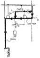
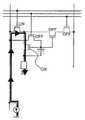
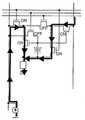
본 발명의 구조는 도 1a에 도시된다. 도 1a의 픽셀은, 소스 신호 라인(101), 제 1 및 제 2 게이트 신호 라인(102, 103), 전류 공급 라인(104), 제 1 스위칭 소자(105), 제 2 스위칭 소자(106), 구동 TFT(107), 변환 및 구동 TFT(108), 저장 커패시터(109), EL 소자(110), 신호 전류를 입력하는 전류 소스(111)를 구비한다.The structure of the present invention is shown in FIG. 1A. The pixel of FIG. 1A includes a
저장 커패시터(109)는 배선, 활성층, 게이트 재료 등과 그 사이의 절연층을 이용하여 용량성 소자로서 형성될 수 있으며, 또한 트랜지스터 게이트 커패시터를 대신 이용함으로써 생략될 수도 있다. 즉, 요구되는 시간 기간에는 변환 및 구동 트랜지스터(108)의 게이트와 소스 사이의 전압을 저장할 수 있다면, 어떠한 구조라도 이용될 수 있다.The
제 1 스위칭 소자(105)는 제 1 게이트 신호 라인(102)에 의해 제어된다. 제 1 스위칭 소자(105)의 제 1 전극은 소스 신호 라인(101)에 접속되고, 제 1 스위칭 소자(105)의 제 2 전극은 구동 TFT(107)의 제 1 전극과 변환 및 구동 TFT(108)의 제 1 전극에 접속된다. 제 2 스위칭 소자(106)는 제 2 게이트 신호 라인(103)에 의해 제어된다. 제 2 스위칭 소자(106)의 제 1 전극은 구동 TFT(107)와 변환 및 구동 TFT(108)의 게이트 전극에 접속되고, 제 2 스위칭 소자(106)의 제 2 전극은 소스 신호 라인(101)에 접속된다. 구동 TFT(107)의 제 2 전극은 EL 소자(110)의 애노드에 접속되고, 변환 및 구동 TFT(108)의 제 2 전극은 전류 공급 라인(104)에 접속된다. 저장 커패시터(109)는 변환 및 구동 TFT(108)의 게이트 전극과 제 2 전극 사이에 접속되고, 변환 및 구동 TFT(108)의 게이트와 소스 사이의 전압을 저장한다. 미리 결정된 전위들은 전류 공급 라인(104) 및 EL 소자(110)의 캐소드에 입력되며, 따라서 상호 전위차를 가진다.The
저장 커패시터(109)는 변환 및 구동 TFT(108)의 게이트와 소스 사이에 접속되는 것이 바람직하다.The
제 1 및 제 2 스위칭 소자는 다른 TFT와 동일한 구조를 가지는 TFT들을 이용하여 형성될 수 있다. 제 1 스위칭 소자(105) 및 제 2 스위칭 소자(106)가 스위칭 TFT(155) 및 저장 TFT(156)로 각각 형성되는 일례가 도 1b에 도시된다. 스위칭 TFT(155) 및 저장 TFT(156)만이 턴온 및 턴오프에 의해 도전 또는 비도전을 선택하는 스위치로서 동작하므로, 극성에 대해서는 어떠한 제한도 없다.The first and second switching elements can be formed using TFTs having the same structure as other TFTs. An example in which the
실시예 모드 1에 한정되지 않고, 스위칭 소자로서 TFT들을 이용할 경우 TFT 극성에 대하여 전혀 제한이 없다. 또한, 트랜지스터, 구체적으로 TFT들이 이용되어도, 단일 결정 실리콘 또는 SOI에 형성되는 트랜지스터들도 이용될 수 있다.The embodiment is not limited to
신호 전류 기입에서 발광까지의 동작은 도 2a 내지 2e를 이용하여 설명된다. 도면 내에서 각 부분을 나타내는 참조 부호는 도 1a 및 1b를 기초로 한다. 도 2a 내지 2c는 신호 입력, 신호 입력 완료, 발광 동안의 각각의 전류 흐름을 개략적으로 도시하고 있다. 도 2d는 신호 전류의 기입 동안의 각 경로에 흐르는 전류들 사이의 관계를 도시하며, 도 2e는 동일한 신호 전류의 기입 동안의 저장 커패시터에 저장되는 전압, 즉 TFT(108)의 게이트와 소스 사이의 전압을 도시한다.The operation from signal current writing to light emission is explained using Figs. 2A to 2E. Reference numerals representing the parts in the drawings are based on FIGS. 1A and 1B. 2A to 2C schematically show respective current flows during signal input, signal input completion, and light emission. FIG. 2D shows the relationship between the currents flowing in each path during the writing of the signal current, and FIG. 2E shows the voltage stored in the storage capacitor during the writing of the same signal current, i.e., between the gate and the source of the
처음에, 펄스는 제 1 게이트 신호 라인(102), 제 2 게이트 신호 라인(103)에 입력되고, 스위칭 TFT(155) 및 저장 TFT(156)는 턴온된다. 이 때, 소스 신호 라인에 흐르는 신호 전류는 Idata로 간주된다.Initially, a pulse is input to the first
전류 Idata는 소스 신호 라인에 흐르고, 그것에 의해 픽셀내의 전류 경로는 도 2a에 도시된 바와 같이 I1과 I2로 나누어진다. 이 두 전류의 관계식은 도 2d에 도시된다. Idata=I1+ I2이다. 또한, 구동 TFT(107)의 게이트 전극의 전위는, 스위칭 TFT(155) 및 저장 TFT(156)가 모두 턴온되어 이 때 구동 TFT(107)의 입력 전극의 전위와 동일하게 된다. 즉, 게이트와 소스간이 전압은 제로가 되고, 이것에 의해 구동 TFT(107) 자체는 턴오프된다. 구동 TFT(107)가 이 상태에서 턴온된다고 가정할 경우, EL 소자(111)에 전류가 흐르고 전류 Idata는 정확하게 설정될 수 없다.The current Idata flows in the source signal line, whereby the current path in the pixel is divided into I1 and I2 as shown in FIG. 2A. The relationship between these two currents is shown in Figure 2d. Idata = I1 + I2 to be. The potential of the gate electrode of the driving
전하는 스위칭 TFT(155)가 턴온되는 순간에 저장 커패시터(109)에 아직 저장되지 않기 때문에, 변환 및 구동 TFT(108)는 턴오프된다. 결국, I2=0, Idata=I1가 된다. 즉, 전류는 상기 기간에는 저장 커패시터(109)의 전하의 저장에 의해서만 흐르게 된다.Since the charge is not yet stored in the
전하는 저장 커패시터(109)에 점차 저장되고, 전위차는 양 전극 사이에서 발생하기 시작한다(도2d 참조). 변환 및 구동 TFT(108)는 양 전극 사이의 전위차가 Vth(도 2e에서 점 A)를 초과할 때 턴온되며, 이것에 의해 I2가 발생한다. 전술된 바와 같이, Idata=I1+I2가 되며, 이것에 의해 I1은 점차 감소된다. 전류는 여전히 흐르게 되고, 또한 전하는 저장 커패시터에 저장된다.Electric charge is gradually stored in the
전하는 저장 커패시터(109)의 양 전극의 전위차, 즉 변환 및 구동 TFT(108)의 게이트와 소스 사이의 전압(VGS)이 소망의 전압이 될 때까지, 즉 변환 및 구동 TFT(108)에 전류 Idata가 흐를 수 있게 하는 전압(VGS)이 될 때까지 저장 커패시터(109)에 계속해서 저장된다. 전하의 저장이 완료될 때(도 2e의 점 B), 전류 I1은 흐름을 정지하고, 또 이 때 VGS에 대응하는 전류가 변환 및 구동 TFT(108)에 흐르게 되고, Idata=I2가 된다(도 2b 참조). 제 2 게이트 신호 라인(103)의 선택이 종료되고, 저장 TFT(156)는 턴오프되며, 신호 기입 동작은 종료된다.The charge is applied to the current I through the conversion and driving
발광 동작은 다음에 다룬다. 스위칭 TFT(155)는 제 1 게이트 신호 라인(102)의 선택이 종료될 때 턴오프된다. 전류 공급 라인에서 스위칭 TFT(105) 및 전류 소스로의 전류 경로가 따라서 차단되며, 이것에 의해 변환 및 구동 TFT(108)에 전류 Idata가 어느 정도까지 흐를 수 있도록 저장 커패시터(109)에 저장된 전하의 일부는 구동 TFT(107)의 게이트 전극에 전달된다. 따라서, 구동 TFT(107)는 자동 턴온된다. 결국, 전류 공급 라인에서 변환 및 구동 TFT(108)로, 구동 TFT(107)로, EL 소자(110)로의 전류 경로는 도 2c에 도시되는 바와 같이 나타나며, 전류 IEL이 흐르게 된다. 따라서, EL 소자(110)가 발광하게 된다.The light emission operation is discussed next. The switching
변환 및 구동 TFT(108)의 게이트 전극 및 구동 TFT(107)의 게이트 전극은 접속되며, 이것에 의해 변환 및 구동 TFT(108) 및 구동 TFT(107)는 이 때 하나의 멀티-게이트 TFT로서 동작한다. 통상적으로, TFT의 게이트 길이(L)가 길어지게 되면, 드레인 전류는 작아지게 된다. 이 경우에, 전류는 신호 기입 동작 동안에 변환 및 구동 TFT(108)에서만 흐르게 되는 Idata이고, 전류는 발광 동안에 변환 및 구동 TFT(108) 및 구동 TFT(107)에 흐르게 되는 IEL이다. 이것에 의해 게이트 전극의 수는 발광 동안에 커지게 되고, 게이트 길이(L)가 결국 더 길어지게 되며, 전류 사이의 관계는 Idata>IEL가 된다.The gate electrode of the conversion and driving
구동 TFT(107)의 채널 폭(W)과 변환 및 구동 TFT(108)의 채널 폭(W)은 동일 크기일 수 있고, 또 상이할 수도 있다. 게이트 길이(L) 사이의 관계는 또한 유사하다.The channel width W of the driving
신호 기입 내지 발광 동작은 전술된 절차들에 따라 실행된다. 본 발명에 따르면, 기입은 또한 전류 Idata를 이용하여 실행될 수도 있으며, 이 전류는 낮은 그레이 스케일로 EL 소자에 의해 발광되는 경우들에 대해서 기입 동안에 EL 소자에 흐르는 전류 IEL보다 더 크다. 따라서, 신호 전류에 삽입되는 잡음과 같은 트러블은 방지될 수 있으며, 고속 기입 동작이 가능하게 된다.The signal writing to light emitting operation is executed in accordance with the above-described procedures. According to the present invention, writing may also be performed using the current Idata , which is larger than the current IEL flowing in the EL element during writing for the cases where it is emitted by the EL element at low gray scale. Therefore, troubles such as noise inserted into the signal current can be prevented, and a high speed write operation is enabled.
또한, 구동 TFT(107) 및 변환 및 구동 TFT(108)는 발광 동안에 멀티-게이트 TFT로서 동작하며, 이것에 의해 이 TFT들은 동일 극성을 가지는 것이 바람직하다. 또한, 전류가 도 2a 내지 2e의 방향으로 흐르는 경우에 극성은 p-채널이 바람직하다.Further, the driving
EL 소자(110)에 흐르는 전류의 방향이 도 2a 내지 2e의 방향과 반대인 경우에 구조는 용이하게 변경될 수 있다. 이러한 구조들은 도 36a 내지 36c에 도시된다. 변환 및 구동 TFT 및 구동 TFT의 극성은 도 2a 내지 2e에 이용되는 극성과는 반대이다. 신호 전류 기입 및 발광 동안의 전류 경로는 도 36b 및 36c에 도시된 바와 같다.The structure can be easily changed when the direction of the current flowing through the
또한, 변환 및 구동 TFT(108)는 신호 기입 및 발광 동안에 이용된다. 즉, TFT 특성들 분산은 신호 기입 및 발광 동안에 공통 TFT들의 일부를 이용함으로써 신호 기입 동작 및 발광 동작에 덜 영향을 미칠 수 있다.In addition, the converting and driving
또, 저장 커패시터(109)에 저장되는 전하의 일부는, 도 2b의 상태에서 도 2c의 상태로 이동할 때 발광들이 개시하는 순간에 구동 TFT(107)의 게이트 전극에 전송된다. 이것에 의해, 저장 커패시터(108)에 저장되는 TFT(108)의 게이트와 소스 사이의 전압은 기입 동안의 소망의 값보다 발광 동안에 다소 작게 된다. 따라서, TFT의 게이트와 소스 사이의 전압은 전류의 흐름을 보다 어렵게 하는 방향으로 매우 조금 이동하고, TFT 오프 누설 전류로 인한 블랙 디스플레이 동안의 소자의 발광은 또한 TFT들(107, 108)의 특성에 분산이 있는 경우에 방지될 수도 있다.In addition, a part of the electric charge stored in the
실시예 모드 1에서, 스위칭 TFT(155) 및 저장 TFT(156)는 제 1 게이트 신호 라인(102) 및 제 2 게이트 신호 라인(103) 각각에 의해 턴온 및 턴오프되도록 제어된다. 턴온 및 턴오프 제어는 신호 기입 완료 직후에 EL 소자가 발광하는 경우들에 동시에 실행될 수 있다. 이것에 의해 게이트 신호 라인의 개수는, 스위칭 TFT(155) 및 저장 TFT(156)의 게이트 전극들을 동일 게이트 신호 라인에 접속하고 스위칭 TFT(155) 및 저장 TFT(156)가 동일 극성을 가지는 경우에 제어를 실행함으로써 감소될 수 있다.In
EL 소자(110)가 구동 TFT(107)와 변환 및 구동 TFT(108)에 의해 구동되는 부하로서 이용된다는 가정하에 설명이 부여되고 상기가 발광 디바이스의 픽셀에 적용됨을 주목하며, 본 발명은 이러한 이용에 한정되지 않는다. 즉, 다이오드, 트랜지스터, 커패시터, 저항기, 또는 이러한 부하들이 결합된 회로를 구동하는 것도 가능하다. 이것은 다른 실시예 모드 및 실시예와 동일하다.Note that explanation is given on the assumption that the
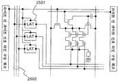
실시예 모드 2
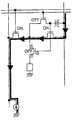
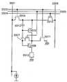
본 발명의 실시예 모드 2는 도 28a에 도시된다. 도 28a의 픽셀은, 소스 신호 라인(2801), 제 1 및 제 2 게이트 신호 라인(2802, 2803), 전류 공급 라인(2804), 제 1 스위칭 소자(2805), 제 2 스위칭 소자(2806), 구동 TFT(2807), 변환 및 구동 TFT(2808), 저장 커패시터(2809), EL 소자(2810)를 구비한다. 각각의 소스 신호 라인은 신호 전류를 입력하는 전류 소스(2811)를 구비한다.
저장 커패시터(2809)는 배선, 활성층, 게이트 재료 등과 그 사이의 절연층을 이용하여 용량성 소자로서 형성될 수 있으며, 또한 트랜지스터 게이트 커패시터를 대신 이용함으로써 생략될 수도 있다. 즉, 요구되는 시간 기간 동안에 변환 및 구동 TFT(2808)의 게이트와 소스 사이의 전압을 저장할 수 있다면, 어떠한 구조라도 이용될 수 있다.The
제 1 스위칭 소자(2805)는 제 1 게이트 신호 라인(2802)에 의해 제어된다. 제 1 스위칭 소자(2805)의 제 1 전극은 소스 신호 라인(2801)에 접속되고, 제 1 스위칭 소자(2805)의 제 2 전극은 구동 TFT(2807)의 제 1 전극과 변환 및 구동 TFT(2808)의 제 1 전극에 접속된다. 제 2 스위칭 소자(2806)는 제 2 게이트 신호 라인(2803)에 의해 제어된다. 제 2 스위칭 소자(2806)의 제 1 전극은 소스 신호 라인(2801)에 접속되고, 제 2 스위칭 소자(2806)의 제 2 전극은 변환 및 구동 TFT(2807) 및 구동 TFT(2807)의 게이트 전극에 접속된다. 구동 TFT(2807)의 제 2 전극은 전류 공급 라인(2804)에 접속되고, 변환 및 구동 TFT(2808)의 제 2 전극은 EL 소자(2810)의 한 전극에 접속된다. 저장 커패시터(2809)는 변환 및 구동 TFT(2808)의 게이트 전극과 제 2 전극 사이에 접속되고, 변환 및 구동 TFT(2808)의 게이트와 소스 사이의 전압을 저장한다. 미리 결정된 전위들은 전류 공급 라인(2804) 및 EL 소자(2810)의 다른 전극 입력되며, 따라서 상호 전위차를 가진다.The
저장 커패시터(2809)는 변환 및 구동 TFT(2808)의 게이트와 소스 사이에 접속되는 것이 바람직하다.The
제 1 및 제 2 스위칭 소자는 다른 TFT들과 동일한 구조를 가지는 TFT들을 이용하여 형성될 수 있다. 제 1 스위칭 소자(2805) 및 제 2 스위칭 소자(2806)가 스위칭 TFT(2855) 및 저장 TFT(2856)로 각각 형성되는 일례가 도 28b에 도시된다. 스위칭 TFT(2855) 및 저장 TFT(2856)만이 턴온 및 턴오프에 의해 도전 또는 비도전을 선택하는 스위치로서 동작하므로, 극성에 대해서는 어떠한 제한도 없다.The first and second switching elements can be formed using TFTs having the same structure as other TFTs. An example in which the
신호 전류 기입에서 발광까지의 동작은 도 29a 내지 29e를 이용하여 설명된다. 도면 내에서 각 부분을 나타내는 참조 부호는 도 28a 및 28b를 기초로 한다. 도 29a 내지 29c는 신호 입력, 신호 입력 완료, 발광 동안의 각각의 전류 흐름을 개략적으로 도시하고 있다. 도 29d는 신호 전류의 기입 동안의 각 경로에 흐르는 전류 사이의 관계를 도시하며, 도 29e는 동일한 신호 전류의 기입 동안의 저장 커패시터에 저장되는 전압, 즉 TFT(2808)의 게이트와 소스 사이의 전압을 도시한다.The operation from signal current write to light emission is explained using Figs. 29A to 29E. Reference numerals representing the parts in the drawings are based on FIGS. 28A and 28B. 29A to 29C schematically show respective current flows during signal input, signal input completion, and light emission. FIG. 29D shows the relationship between the currents flowing in each path during the writing of the signal current, and FIG. 29E shows the voltage stored in the storage capacitor during the writing of the same signal current, that is, the voltage between the gate and the source of the
처음에, 펄스들은 제 1 게이트 신호 라인(2802), 제 2 게이트 신호 라인(2803)에 입력되고, 스위칭 TFT(2855) 및 저장 TFT(2856)는 턴온된다. 이 때, 소스 신호 라인(2801)에 입력되는 신호 전류는 Idata로 간주된다.Initially, pulses are input to the first
전류 Idata는 소스 신호 라인(2801)에 흐른다. 도 29a에 도시되는 픽셀 내에 전류 경로가 있으며, Idata가 이 경로에 흐르고, I1과 I2로 분리된다. Idata=I1+ I2이다. 또한, 구동 TFT(2807)의 게이트 전극의 전위는 스위칭 TFT(2855) 및 저장 TFT(2856)가 모두 턴온되어 이 때 구동 TFT(2807)의 제 2 전극의 전위와 동일하게 된다. 즉, 게이트와 소스간이 전압은 제로가 되고, 이것에 의해 구동 TFT(2807) 자체는 턴오프된다. 구동 TFT(2807)가 이 상태에서 턴온된다고 가정할 경우, EL 소자(2810)에 전류가 흐르고, 전류 Idata는 정확하게 설정될 수 없다.Current Idata flows in the
전하는 스위칭 TFT(2855)가 턴온되는 순간에 저장 커패시터(2809)에 아직 저장되지 않기 때문에, 변환 및 구동 TFT(2808)는 턴오프된다. 결국, I2=0, Idata=I1가 된다. 즉, 전하는 저장 커패시터(2809)에 저장되고, 이에 대응하는 전류가 발생된다.Since the charge is not yet stored in the
전하는 저장 커패시터(2809)에 점차 저장되고, 전위차는 양 전극 사이에서 발생하기 시작한다. 변환 및 구동 TFT(2808)는 양 전극 사이의 전위차가 Vth, 즉 변환 및 구동 TFT(2808)의 문턱값(도 29e에서 점 A)에 도달할 때 턴온되며, 이것에 의해 I2가 발생한다. 전술된 바와 같이, Idata=I1+I2가 되며, 이것에 의해 I1은 점차 감소되지만, 저장 커패시터(2809)에의 전하 저장이 완료될 때까지 제로에 도달하지 않으며, 전류는 여전히 흐르게 된다.Electric charge is gradually stored in the
전하는 저장 커패시터(2809)의 양 전극의 전위차, 즉 변환 및 구동 TFT(2808)의 게이트와 소스 사이의 전압이 소망의 전압이 될 때까지, 즉 변환 및 구동 TFT(2808)에 전류 Idata가 흐를 수 있게 하는 전압(VGS)이 될 때까지 저장 커패시터(2809)에 계속해서 저장된다. 전하의 저장이 완료될 때(도 29e의 점 B), 전류 I1는 흐름을 정지하고, 또 이 때 VGS에 대응하는 전류가 변환 및 구동 TFT(2808)에 흐르게 되고, Idata=I2가 된다(도 29b 참조). 제 2 게이트 신호 라인(2803)의 선택이 완료되고, 저장 TFT(2856)는 턴오프된다. 제 1 게이트 신호 라인(2802)의 선택이 완료되고, 스위칭 TFT(2855)는 턴오프되고, 신호 기입 동작은 완료된다.The charge flows through the current Idata until the potential difference between the two electrodes of the
발광 동작은 다음에 다룬다. 스위칭 TFT(2855)는 제 1 게이트 신호 라인(2802)의 선택이 종료될 때 턴오프된다. 따라서, 소스 신호 라인(2801)에서 스위칭 TFT(2855)로, 변환 및 구동 TFT(2808)로, EL 소자(2810)로의 전류 경로는 차단되며, 이것에 의해 변환 및 구동 TFT(2808)에 전류 Idata가 어느 정도까지 흐르도록 저장 커패시터(2809)에 저장된 전하의 일부는 구동 TFT(2807)의 게이트 전극에 전달된다. 따라서, 구동 TFT(2807)는 자동 턴온된다. 결국, 전류 공급 라인(2804)에서 구동 TFT(2807)로, 변환 및 구동 TFT(2808)로, EL 소자(2810)로의 전류 경로는 도 29c에 도시된 바와 같으며, 발광 전류 IEL이 흐르게 된다. EL 소자(2810)가 발광하게 된다.The light emission operation is discussed next. The switching
변환 및 구동 TFT(2808)의 게이트 전극과 구동 TFT(2807)의 게이트 전극은 접속되며, 이것에 의해 변환 및 구동 TFT(2808) 및 구동 TFT(2807)는 이 때 한 멀티-게이트 TFT로서 동작한다. 통상적으로, TFT의 게이트 길이(L)가 길어지게 되면, 드레인 전류는 작아지게 된다. 이 경우에, 따라서 신호 전류는 신호 전류 기입 동작 동안에 변환 및 구동 TFT(2808)에서만 흐르게 되고, 발광 전류는 발광 동안에 변환 및 구동 TFT(2808) 및 구동 TFT(2807)에 흐르게 된다. 이것에 의해 게이트 전극의 개수는 발광 동안에 커지게 되고, 게이트 길이(L)는 결국 더 길어지게 되며, 전류 사이의 관계는 Idata>IEL가 된다.The gate electrode of the conversion and driving
구동 TFT(2807)의 채널 폭(W)과 변환 및 구동 TFT(2808)의 채널 폭(W)은 동일 크기일 수 있고, 또 상이할 수도 있다. 또한, 게이트 길이(L) 사이의 관계는 유사하다.The channel width W of the driving
신호 전류 기입 내지 발광은 전술된 절차에 따라 실행된다. 본 발명에 따르면, 기입은 또한 신호 전류 Idata를 이용하여 실행될 수도 있으며, 이 전류는 낮은 그레이 스케일로 EL 소자에 의해 발광되는 경우에 대해서 기입 동안에 발광 전류 IEL보다 더 크다. 또한, EL 소자가 부하가 되는 경우에도, 상당히 큰 전류에서 기입을 실행함으로써 기입 시간 양을 단축하는 것이 가능하게 된다.Signal current writing to light emission is performed in accordance with the above-described procedure. According to the present invention, writing may also be performed using the signal current Idata , which is larger than the luminous current IEL during writing for the case where it is emitted by the EL element at a low gray scale. In addition, even when the EL element is loaded, it is possible to shorten the amount of writing time by performing writing at a considerably large current.
또한, 구동 TFT(2807) 및 변환 및 구동 TFT(2808)는 발광 동안에 멀티-게이트 TFT로서 동작하며, 이것에 의해 이 TFT는 동일 극성을 가지는 것이 바람직하다. 또한, 전류가 도 29a 내지 29e의 방향으로 흐르는 경우에 극성은 n-채널이 바람직하다.Further, the driving
또, 실시예 모드 1에서 행해진 설명과 동일하게 EL 소자에 흐르는 전류의 방향이 반대인 경우에 구조는 용이하게 변경될 수 있다. 이러한 구조는 도 37a에 도시된다. 변환 및 구동 TFT 및 구동 TFT의 극성은 도 29a 내지 29e에 이용되는 극성과는 반대이다. 신호 전류 기입 및 발광 동안의 전류 경로들은 도 37b 및 37b에 도시된 바와 같다. 또한, 본 상세의 후속 실시예에 대해서도 동일한 변경이 가능하며, 이것에 의해 그 이후 설명은 생략된다.In addition, the structure can be easily changed in the case where the direction of the current flowing through the EL element is reversed, similarly to the explanation made in
또한, 변환 및 구동 TFT(2808)는 신호 기입 및 발광 동안에 이용된다. 즉, TFT 특성들 분산은 신호 기입 및 발광 동안에 공통 TFT의 일부를 이용함으로써 신호 기입 동작들 및 발광 동작에 덜 영향을 미칠 수 있다.In addition, the converting and driving
또, 저장 커패시터(2809)에 저장되는 전하의 일부는, 도 29b의 상태에서 도 29c의 상태로 이동할 때 발광이 개시하는 순간에 구동 TFT(2807)의 게이트 전극에 전송된다. 이것에 의해, 저장 커패시터(2809)에 저장되는 TFT(2808)의 게이트와 소스 사이의 전압은 기입 동안의 소망의 값보다 발광 동안에 다소 작게 된다. 결국, TFT의 게이트와 소스 사이의 전압은 전류의 흐름을 보다 어렵게 하는 방향으로 매우 조금 이동하고, TFT 오프 누설 전류로 인한 블랙 디스플레이동안의 소자의 발광은 또한 TFT들(2807, 2808)의 특성에 분산이 있는 경우에 방지될 수도 있다.A part of the electric charge stored in the
실시예 모드 2에서, 스위칭 TFT(2855) 및 저장 TFT(2856)는 제 1 게이트 신호 라인(2802) 및 제 2 게이트 신호 라인(2803) 각각에 의해 턴온 및 턴오프되도록 제어된다. 턴온 및 턴오프 제어는 신호 기입 완료 직후에 EL 소자가 발광하는 경우들에 동시에 실행될 수 있다. 이것에 의해 게이트 신호 라인의 개수는, 스위칭 TFT(2855) 및 저장 TFT(2856)의 게이트 전극을 동일 게이트 신호 라인에 접속하고 스위칭 TFT(2855) 및 저장 TFT(2856)가 동일 극성을 가지는 경우에 제어를 실행함으로써 감소될 수 있다.In
본 발명의 실시예 모드 1 및 실시예 2의 구조가 표 1에 부가된 비교가 표 2에 도시된다.A comparison in which the structures of

또한, 본 발명의 주요 관점은, 신호 전류 입력을 수신하여, 임의 타이밍에서 전류의 저장을 실행하고, 출력 샘플 및 홀드 동작동안에 멀티-게이트 TFT들로서 전류 경로가 되는 TFT들을 이용하는 것이다. EL 소자들을 이용하여 발광 디바이스의 픽셀에 대한 실시예 모드가 통상적으로 본 명세에 제공되고 있지만, 본 발명은 이러한 이용에 한정되지 않으며. 특히 진폭 변환 회로들과 같은 아날로그 회로에 본 발명을 적용하는데 효과적이기도 하다.Also, the main aspect of the present invention is to receive the signal current input, execute the storage of the current at an arbitrary timing, and use the TFTs which become the current path as the multi-gate TFTs during the output sample and hold operation. While an embodiment mode for a pixel of a light emitting device using EL elements is typically provided in the present specification, the present invention is not limited to this use. It is particularly effective in applying the present invention to analog circuits such as amplitude conversion circuits.
실시예Example
본 발명의 실시예가 이하에서 논의된다.Embodiments of the present invention are discussed below.
실시예 1Example 1
아날로그 이미지 신호를 이용하여 디스플레이를 실행하는 반도체 디바이스의 구조는 실시예 1에서 설명된다. 반도체 디바이스의 구조에 관한 일례가 도 3a에 도시된다. 복수의 픽셀이 매트릭스 형태로 기판(301)에 배열되는 픽셀부(302)가 있다. 소스 신호 라인 구동 회로(303), 제 1 및 제 2 게이트 신호 라인 구동 회로(304, 305)는 그 픽셀부(302) 주변에 있다. 2개의 게이트 신호 라인 구동 회로가 도 3a에 이용되는 경우에도, 실시예 모드에서 설명된 바와 같이 픽셀 구동을 위해 복수의 게이트 신호 라인을 선택할 필요가 없는 경우에 단지 1개만이 요구된다. 또한, 게이트 신호 라인 구동 회로들이 게이트 신호 라인들의 양 단부에 대칭적으로 배치되고, 게이트 신호 라인들이 양 단부로부터 구동되는 구조가 이용될 수도 있다.The structure of the semiconductor device for performing the display using the analog image signal is described in
소스 신호 라인 구동 회로(303), 제 1 게이트 신호 라인 구동 회로(304), 제 2 게이트 신호 라인 구동 회로(305)에 입력되는 신호는 가요성 인쇄 회로(FPC)(306)를 통해 외부에서 공급된다.Signals input to the source signal
소스 신호 라인 구동 회로의 구조에 관한 일례는 도 3b에 도시된다. 소스 신호 라인 구동 회로는, 이미지 신호로서 아날로그 이미지 신호를 이용하여 디스플레이를 실행하기 위한 것이며, 시프트 레지스터(311), 버퍼(312), 샘플링 회로(313), 전류 변환 회로(314)를 구비한다. 도면에 구체적으로 도시되지 않은 레벨 시프터들 등은 필요할 경우 부가될 수도 있다.An example of the structure of the source signal line driving circuit is shown in FIG. 3B. The source signal line driving circuit is for performing display using an analog image signal as an image signal, and includes a
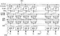
소스 신호 라인 구동 회로의 동작은 다음에 설명된다. 관련되는 상세 구조는 도 8에 도시된다.The operation of the source signal line driver circuit is described next. The detailed structure involved is shown in FIG. 8.
시프트 레지스터(801)는 복수 단의 플립플롭 회로(FF) 등을 이용함으로써 행해지고, 클럭 신호(S-CLK), 클럭 반전 신호(S-CLKb) 및 개시 펄스(S-SP)를 입력한다. 샘플링 펄스들은 상기 신호들의 타이밍에 따라 차례로 출력된다.The
시프트 레지스터(801)로부터 출력되는 샘플링 펄스들은 버퍼(802) 등을 통해 증폭된 후에 샘플링 회로에 입력된다. 샘플링 회로(803)는 복수 단의 샘플링 스위치들(SW)을 이용하여 제조되며, 입력 샘플링 펄스들의 타이밍에 따라 이미지 신호의 임의 컬럼의 샘플링을 실행한다. 구체적으로, 샘플링 스위치들은 샘플링 펄스들이 샘플링 스위치들에 입력되는 경우에 턴온되고, 그 때의 이미지 신호의 전위는 샘플링 스위치들을 통해 전류 변환 회로(804)에 입력된다.The sampling pulses output from the
전류 변환 회로(804)는 복수 단의 전류 세팅 회로들(810)을 이용하여 제조되며, 샘플링된 이미지 신호에 따라 미리 결정된 전류(Si,1≤i≤n)를 소스 신호 라인에 출력한다. 전류 세팅 회로들(810)의 동작은 도 10을 이용하여 이하에서 설명된다.The
도 10은 샘플링 회로 및 전류 변환 회로의 구조를 도시하는 도면이다. 샘플링 회로(1001)의 동작은 전술된 바와 같다. 여기서 샘플링 스위치(1002)로 1개의 TFT를 이용하는 경우에도, n-채널 TFT 및 p-채널 TFT를 이용하여 구성되는 아날로그 스위치들 등이 이용될 수도 있다.10 is a diagram illustrating the structures of a sampling circuit and a current conversion circuit. The operation of the
전류 변환 회로(1003)는 전류 출력 회로(1004) 및 리셋 회로(1005)를 구비하고, 샘플링된 전압 신호를 전류 신호로 변환한다. 이미지 신호는 전류 출력 회로(1004)에 입력되고, 미리 결정된 전류(Idata)는 출력 이미지 신호의 전위에 따라 출력된다. 전류 출력 회로는 도 10의 TFT 및 연산 증폭기를 이용하여 구성되지만, 이러한 구조에 특히 한정되지 않는다. 입력 신호의 전위에 따라 미리 결정된 신호 전류를 출력할 수 있는 경우에는 다른 구조들이 이용될 수도 있다.The
전류 출력 회로(1004)로부터 출력되는 신호 전류는 리셋 회로(1005)에 입력된다. 리셋 회로(1005)는 아날로그 스위치들(1006, 1007), 인버터(1008), 전원(1009)를 구비한다.The signal current output from the
아날로그 스위치들(1006, 1007) 모두는 리셋 신호(Res.) 및 인버터(1008)에 의해 반전되는 리셋 신호를 이용하여 제어되고, 다른 것이 온으로 되는 경우에는 하나는 오프로 되도록 동작한다.Both
리셋 신호는 정상적인 기입 동안에 입력되지 않으며, 이것에 의해 아날로그 스위치(1006)는 온으로 되고, 아날로그 스위치(1007)는 오프로 된다. 전류 출력 회로(1004)로부터 출력되는 신호 전류는 이 때 소스 신호 라인에 출력된다. 한편, 아날로그 스위치(1006)는 리셋 신호가 입력되는 경우에 턴오프되고, 아날로그 스위치(1007)는 턴온된다. 전원(1009)에 의해 부여되는 전위는 소스 신호 라인의 전위로서 인가되고, 소스 신호 라인은 리셋된다. 리셋 동작은 수평 리턴 기간 등의 동안에 실행된다. 또한, 전원(1009)로부터 부여되는 전위는 픽셀부의 전류 공급 라인의 전위와 거의 동일한 것이 바람직하다. 즉, 소스 신호 라인에 흐르는 전류의 양은 소스 신호 라인이 리셋되는 경우에 제로로 세팅될 수 있는 것이 바람직하다.The reset signal is not input during normal writing, whereby the
게이트 신호 라인 구동 회로의 구조에 관한 일례는 도 3c에 도시된다. 게이트 신호 라인 구동 회로는 시프트 레지스터(321) 및 버퍼(322)를 구비한다. 회로 동작은 소스 신호 라인 구동 회로와 동일하며, 시프트 레지스터(321)는 클럭 신호 및 개시 펄스에 따라 차례로 펄스들을 출력한다. 펄스들은 버퍼(322)에 의해 증폭된 후에 게이트 신호 라인에 입력되고, 한 로우(row)가 선택된 상태에 동시에 배치된다. 신호 전류는 소스 신호 라인으로부터 순서대로 선택된 게이트 신호 라인에 의해 제어되는 픽셀 컬럼에 기입된다.An example of the structure of the gate signal line driver circuit is shown in Fig. 3C. The gate signal line driver circuit includes a
복수의 플립플롭을 가지는 시프트 레지스터가 시프트 레지스터의 일례로서 도면에 도시되고 있지만, 디코더 등을 이용하여 신호 라인을 선택하는 것이 가능한 구조가 이용될 수도 있다.Although a shift register having a plurality of flip-flops is shown in the figure as an example of the shift register, a structure capable of selecting a signal line using a decoder or the like may be used.
실시예 2Example 2
이미지 신호로 디지털 이미지 신호를 이용하여 디스플레이를 실행하는 반도체 디바이스의 구조는 실시예 2에서 설명된다. 반도체 디바이스의 구조에 관한 일례는 도 4a에 도시된다. 복수의 픽셀이 매트릭스 형태로 배열되는 픽셀부(402)가 있다. 소스 신호 라인 구동 회로(403), 제 1 및 제 2 게이트 신호 라인 구동 회로들(404, 405)는 그 픽셀부(402) 주변에 배치된다. 2개의 게이트 신호 라인 구동 회로들이 도 4a에서 이용되고 있지만, 실시예 모드에서 설명된 바와 같이, 픽셀 구동을 위해 복수의 게이트 신호 라인들을 선택할 필요가 없는 경우에는 단지 1개만이 이용된다. 또한, 게이트 신호 라인 구동 회로들이 게이트 신호 라인들 양단에 대칭적으로 배치되고, 게이트 신호 라인들이 양 단부로부터 구동되는 구조가 이용될 수도 있다.The structure of the semiconductor device for performing the display using the digital image signal as the image signal is described in the second embodiment. An example of the structure of the semiconductor device is shown in Fig. 4A. There is a
소스 신호 라인 구동 회로(403), 제 1 게이트 신호 라인 구동 회로(404) 및 제 2 게이트 신호 라인 구동 회로(405)에 입력되는 신호들은 가요성 인쇄 회로(FPC)(406)로부터 공급된다.Signals input to the source signal
소스 신호 라인 구동 회로의 구조에 관한 일례는 도 4b에 도시된다. 소스 신호 라인 구동 회로는 이미지 신호로서 디지털 이미지 신호를 이용하여 디스플레이를 실행하기 위한 것이며, 시프트 레지스터(411), 제 1 래치 회로(412), 제 2 래치 회로(413), 고정 전류 회로(414)를 구비한다. 특히 도면에 도시되지 않은 레벨 시프터들 등은 필요에 따라 부가될 수도 있다.An example of the structure of the source signal line driving circuit is shown in Fig. 4B. The source signal line driving circuit is for executing a display using a digital image signal as an image signal, and includes a
게이트 신호 라인 구동 회로들(404, 405)은 실시예 1에 도시된 것과 동일하기 때문에 여기 도면에 도시되지 않으며, 그에 대한 설명도 생략된다.Since the gate signal
소스 신호 라인 구동 회로의 동작은 다음에 설명된다. 관련된 상세 구조는 도 9에 도시된다.The operation of the source signal line driver circuit is described next. A related detailed structure is shown in FIG.
시프트 레지스터(901)는 복수단의 플립플롭 회로(FF) 등을 이용하여 제조되며, 클럭 신호(S-CLK), 클럭 반전 신호(S-CLKb) 및 개시 펄스(S-SP)를 입력한다. 샘플링 펄스들은 이 신호들의 타이밍에 따라 차례로 출력한다.The
시프트 레지스터(901)로부터 출력되는 샘플링 펄스는 제 1 래치 회로(902)에 입력된다. 디지털 이미지 신호는 제 1 래치 회로(902)에 입력되고, 디지털 이미지 신호는 샘플링 펄스가 입력되는 타이밍에 따라 각 단에서 저장된다.The sampling pulse output from the
제 1 래치 회로(902)로의 디지털 이미지 신호의 저장이 최종단까지 완료되는 경우, 래치 펄스는 수평 리턴 기간동안에 제 2 래치 회로(903)에 입력되고, 제 1 래치 회로(902)에 저장된 디지털 이미지 신호는 제 2 래치 회로(903)에 한꺼번에 전송된다. 제 2 래치 회로(903)에 저장된 디지털 이미지 신호의 한 로우 부분은 고정 전류 회로(904)에 입력된다.When the storage of the digital image signal to the
제 2 래치 회로(903)에 저장되는 디지털 이미지 신호가 고정 전류 회로(904)에 입력되는 동안에, 샘플링 펄스는 시프트 레지스터(901)에 다시 출력된다. 이미지 신호의 한 프레임 부분의 처리는 상기 동작을 반복하여 실행될 수 있다.While the digital image signal stored in the
도 11는 고정 전류 회로의 구조를 도시하는 도면이다. 고정 전류 회로는 복수 단의 전류 세팅 회로(1101)를 구비한다. 각 단에 형성되는 전류 세팅 회로(1101)는, 미리 결정된 전류(Idata)를 제 2 래치 회로로부터의 디지털 이미지 신호의 1 또는 0 정보에 따라서 소스 신호 라인에 출력한다.11 is a diagram illustrating a structure of a fixed current circuit. The fixed current circuit includes a plurality of stages of
전류 세팅 회로(1101)는 신호 전류, 아날로그 스위치(1103~1106), 인버터(1107, 1108) 및 전원(1109)를 공급하는 고정 전류 소스(1102)를 구비한다. 고정 전류 소스(1102)는 도 11의 TFT 및 연산 증폭기로 구성되지만, 이러한 구조에 특정하게 한정되지 않는다.The
아날로그 스위치들(1103~1106)은 제 2 래치 회로(903)로부터 출력되는 디지털 이미지 신호에 의해 턴온 및 턴오프되도록 제어된다. 아날로그 스위치들(1103, 1104)는 상호 배타적인 방법으로 동작하며, 하나가 턴온되면 나머지는 턴오프된다. 동일하게, 아날로그 스위치들(1105,1106)도 상호 배타적인 방법으로 동작한다.The analog switches 1103 to 1106 are controlled to be turned on and off by the digital image signal output from the
제 2 래치 회로(903)에 저장된 디지털 이미지 신호가 1인 경우, 즉 H 레벨인 경우, 아날로그 스위치들(1103, 1105)은 턴온되고, 아날로그 스위치들(1104, 1106)은 턴오프된다. 이것에 의해, 미리 결정된 신호 전류는 고정 전류 소스(1102)로부터 흐르게 되고, 아날로그 스위치들(1103, 1105)을 통해 소스 신호 라인에 출력된다.When the digital image signal stored in the
한편, 제 2 래치 회로(903)에 저장된 디지털 이미지 신호가 0인 경우, 즉 L 레벨인 경우, 아날로그 스위치들(1104, 1106)은 턴온되고, 아날로그 스위치들(1103, 1105)는 턴오프된다. 이것에 의해, 고정 전류 소스(1102)로부터 출력되는 신호 전류는 소스 신호 라인에 출력되지 않고, 아날로그 스위치(1104)를 통해 접지 레벨로 저하된다. 그러나, 전원(1109)의 전위는 아날로그 스위치(1106)를 통해 소스 신호 라인에 제공된다. 전원(1109)의 전위는 픽셀부의 전류 공급 라인과 거의 동일한 것이 바람직하다. 즉, 소스 신호 라인에 흐르는 전류는 디지털 이미지 신호가 L 레벨인 경우에 제로로 설정될 수 있는 것이 바람직하다.On the other hand, when the digital image signal stored in the
전술된 동작은 한 수평 기간에 있어서 모든 단에 걸쳐 동일하게 실행된다. 따라서, 모든 소스 신호 라인에 출력되는 신호 전류값이 결정된다.The above-described operation is executed equally across all stages in one horizontal period. Thus, signal current values output to all source signal lines are determined.
아날로그 스위치가 전류 세팅 회로에서 스위치로서 이용되지만, 다른 타입의 스위치가 이용될 수도 있다. 예를 들면, 전송 게이트가 이용될 수도 있다. 또한, 실시예 1에서 논의된 바와 같이, 시프트 레지스터 대신에 디코더 등을 이용하여 신호 라인을 선택할 수 있는 또다른 구조가 이용될 수 있다.Although an analog switch is used as a switch in the current setting circuit, other types of switches may be used. For example, a transfer gate may be used. In addition, as discussed in
실시예 3Example 3
디스플레이는, 실시예 2에 도시된 디지털 이미지 신호를 이용하는 반도체 디바이스에서 2개의 그레이 스케일, 화이트 및 블랙으로 이루어진다. 디지털 이미지 신호를 이용하여 복수의 그레이 스케일을 동일하게 디스플레이하는 구동 회로는 실시예 3에서 기술된다.The display is made up of two gray scales, white and black in a semiconductor device using the digital image signal shown in the second embodiment. A driving circuit for equally displaying a plurality of gray scales using a digital image signal is described in the third embodiment.
도 12는 3-비트 디지털 그레이 스케일 디스플레이를 실행하는 소스 신호 라인 구동 회로의 구조에 관한 일례를 도시하고 있다. 소스 신호 라인 구동 회로 동작은 실시예 2에 도시된 1-비트 소스 신호 라인 구동 회로와 동일하고, 시프트 레지스터(1201), 제 1 래치 회로(1202), 제 2 래치 회로(1203), 고정 전류 회로(1204)를 구비한다. 고정 전류 회로(1204)는 실시예 2와 동일하게 복수의 전류 세팅 회로(1210)를 이용한다.Fig. 12 shows an example of the structure of a source signal line driver circuit for executing a 3-bit digital gray scale display. The source signal line driving circuit operation is the same as that of the 1-bit source signal line driving circuit shown in
3-비트 디지털 이미지 신호는 비트 단위로(디지털 데이터 1 내지 3) 입력된다. 제 1 래치 회로(1202) 및 제 2 래치 회로(1203)는 3개 비트와 병렬로 배열되고, 시프트 레지스터로부터 출력되는 샘플링 펄스에 따라 동시에 디지털 이미지 신호의 3개 비트 부분에 관한 저장 동작을 실행한다. 제 2 래치 회로(1203)에 저장된 3-비트 디지털 이미지 신호는 고정 전류 회로(1204)에 입력된다.The 3-bit digital image signal is input bit by bit (
도 13은 실시예 3의 고정 전류 회로를 구성하는 전류 세팅 회로의 구조에 관한 일례를 도시하고 있다. 전류 세팅 회로(1300)는 TFT들(1301~1303), 아날로그 스위치들(1304, 1305), 인버터들(1306, 1307), NOR 회로(1308), 전원들(1309, 1310)를 구비한다.FIG. 13 shows an example of the structure of the current setting circuit constituting the fixed current circuit of
디지털 이미지 신호의 3-비트는 TFT들(1301~1303)의 게이트 전극에 각각 입력되고, NOR 회로(1308)에 입력된다. 그 TFT는 서로 다른 채널 폭(W)을 각각 가지며, 통과 전류는 4:2:1 비율로 세팅된다.3-bits of the digital image signal are input to the gate electrodes of the
TFT들(1301~1303)의 게이트 전극에 입력되는 디지털 이미지 신호가 1인 경우, 즉 H 레벨인 경우, TFT는 턴온되고, 미리 결정된 전류는 소스 신호 라인에 공급된다. 소스 신호 라인에 공급되는 전류는 TFT들(1301~1303)을 통해 공급되는 전류의 합이 되고, 각 TFT의 통과 전류는 전술된 바와 같이 4:2:1 비율을 가지며, 이것에 의해 전류 크기는 23 단, 즉 8 단으로 제어될 수 있다.When the digital image signal input to the gate electrodes of the
TFT들(1301~1303)의 게이트 전극에 입력되는 디지털 이미지 신호가 모두 제로인 경우, 즉 L 레벨인 경우, TFT들(1301~1303) 모두는 턴오프된다. 한편, H 레벨은 NOR로부터 출력되고, 아날로그 스위치(1305)는 턴온되며, 전원(1310)의 전원 전위는 소스 신호 라인에 제공된다.When the digital image signals input to the gate electrodes of the
또한, 리셋 신호(Res.)가 수평 리턴 기간 내에 입력되는 경우, 아날로그 스위치(1304)는 턴온되고, 전원(1309)의 전원 전위는 소스 신호 라인에 제공된다.In addition, when the reset signal Res. Is input within the horizontal return period, the
전원들(1309,1310)의 전위는, 전원 전위가 소스 신호 라인에 제공될 때 소스 신호 라인에 흐르는 전류량이 제로로 설정되도록, 픽셀의 전류 공급 라인과 동일한 전위로 각각 설정된다.The potentials of the
따라서, 그레이 스케일이 실행될 수 있다. 3-비트 디지털 그레이 스케일의 경우에 관한 일례가 실시예 3에서 제공되고는 있지만, 그레이 스케일의 수에 특정하게 한정되지 않으며, 보다 많은 개수의 그레이 스케일이 디스플레이되는 경우에 동일한 방법을 통해 실시예 3을 실행하는 것이 가능하다.Thus, gray scale can be executed. An example of the case of the 3-bit digital gray scale is provided in
실시예 4Example 4
도 1a 및 1b에 도시된 구조들에서, 저장 커패시터 TFT(156)는 소스 신호 라인(101)에 접속된다. 또한, 저장 TFT(156)는 도 14a에 도시되는 스위칭 TFT(1401)의 출력 전극에 접속되고, 또 구동 TFT(1403)의 출력 전극에 접속된다.In the structures shown in FIGS. 1A and 1B, the
신호 기입 및 발광 동작들은 도 14b 내지 14d에 도시되지만, 전류 경로 I2가 도 1a 및 1b와는 다소 서로 다른 것이외의 동작은 동일하기 때문에, 그것에 대한 설명은 생략한다.Signal writing and light emitting operations are shown in Figs. 14B to 14D, but since the operation is the same except that the current path I2 is somewhat different from Figs. 1A and 1B, the description thereof is omitted.
또한, 실시예 4에 도시된 저장 TFT(1402)에 대한 접속을 이용함으로써, 디지털 이미지 신호를 이용하는 타임 그레이 스케일 방법에 의해 구동되는 반도체 디바이스는 리셋 TFT로서 저장 TFT(1402)를 이용할 수 있다. 구동 TFT(1403)의 게이트와 소스 사이의 전압은 제로로 설정될 수 있고, 발광 기간 종료 후에 저장 커패시터 TFT(1402)를 턴온시킴으로써 구동 TFT(1403)를 턴오프시킨다. 따라서, EL 소자로부터의 발광이 정지하게 된다.Further, by using the connection to the
여기에서, 타임 그레이 스케일 방법에 관한 상세 설명을 생략하고 있지만, JP 2001-5426, JP 2000-86968호에 기술된 방법이 참조될 수 있다.Here, although the detailed description about the time gray scale method is omitted, the method described in JP 2001-5426, JP 2000-86968 can be referred to.
상기 구조가 액티브 매트릭스 디스플레이 디바이스에 적용되는 일례는 도 34a 및 34b에 도시된다. 도 34b는 실제 소자 및 배선 레이아웃의 일례이며, 도 34a는 각 소자 사이의 위치 관계를 반영한 동등한 회로도이다. 도면 내의 참조 부호는 도 14a 내지 14d에 기초한다.One example where the above structure is applied to an active matrix display device is shown in FIGS. 34A and 34B. 34B is an example of an actual element and wiring layout, and FIG. 34A is an equivalent circuit diagram which reflects the positional relationship between each element. Reference numerals in the drawings are based on Figs. 14A to 14D.
또한, 동일한 동작은 도 14a 내지 14d와 서로 다른 구조를 이용할 수 있다. 다시 말하면, 도 38a와 동일한 경로는 신호 전류가 입력될 때 설정될 수 있고, 도 38b와 동일한 경로는 발광 동안에 설정될 수 있다. 따라서, 스위칭 소자 등은, 위치가 전술된 경로에 일치하도록 배치될 수 있고, 도 38c와 같은 접속도 가능하다.In addition, the same operation may use a different structure from those of FIGS. 14A to 14D. In other words, the same path as in Fig. 38A can be set when a signal current is input, and the same path as in Fig. 38B can be set during light emission. Thus, the switching element or the like can be arranged so that the position coincides with the above-described path, and a connection as shown in FIG. 38C is also possible.
실시예 5Example 5
이 실시예에서, 반도체 디바이스의 제조 방법이 기술된다. 통상적으로, 구동 회로를 구성하는 n-채널 TFT 및 p-채널 TFT와 픽셀부에 제공되는 TFT가 기술된다. 픽셀을 구성하는 TFT의 일부에 관하여 구체적으로 기술되지 않으며, 이 실시예에 따라 형성될 수 있다.In this embodiment, a method of manufacturing a semiconductor device is described. Typically, n-channel TFTs and p-channel TFTs constituting the driving circuit and TFTs provided in the pixel portion are described. A part of the TFTs constituting the pixel is not specifically described, and may be formed according to this embodiment.
처음에, 도 21a에 도시된 바와 같이, 실리콘 산화물 필름, 실리콘 질화물 필름 또는 실리콘 산화질화물 필름과 같은 절연 필름으로 형성된 베이스 필름(5002)은, 코닝 코오포레이션의 #7059 유리 및 #1737 유리로 디스플레이되는 바륨 보로실리케이트 유리 또는 알루미노 보로실리케이트 유리 등의 유리로 형성되는 기판(5001)에 형성된다. 예를 들면, 플라즈마 CVD 방법에 의해 SiH4, NH3, N2O로 형되고 10 내지 200nm(바람직하게는, 50 내지 100nm)의 두께를 가지는 실리콘 산화질화물 필름(5002a)이 형성된다. 동일하게는, SiH4, 및 N2O으로 형성되고 두께가 10 내지 200nm(바람직하게는 50 내지 100nm)인 수소화된 실리콘 산화질화물 필름은 그 위에 적층된다. 이 실시예에서, 베이스 필름(5002)은 2-층 구조를 가지지만, 상기 절연 필름 중 하나로 이루어진 단일 층 필름으로서 형성되거나, 또는 상기 절연층 중 2개 층이상을 가지는 적층 필름으로서 형성될 수 있다.Initially, as shown in FIG. 21A, a
아일랜드형 반도체층들(5003~5006)은 비결정성 구조를 갖는 반도체 필름에 레이저 결정화 방법 또는 공지된 열적 결정화 방법을 행함으로써 얻어지는 결정 반도체 필름으로 형성된다. 이 아일랜드형 반도체층들(5003~5006)은 각각 두께가 25 내지 80nm(바람직하게는 30 내지 60nm)이다. 결정 반도체 필름의 재료에 대해서 전혀 한정되지 않지만, 결정 반도체 필름은 실리콘, 실리콘 게르마늄(SiGe) 합금 등으로 형성되는 것이 바람직하다.The island
결정 반도체 필름이 레이저 결정화 방법으로 제조되는 경우, 연속 발진형 또는 연속 발광형의 엑시머 레이저, YAG 레이저 및 YVO4 레이저가 이용된다. 이러한 레이저가 이용되는 경우, 레이저 발진으로부터 방사되는 레이저빔이 광학 시스템에 의해 직선 형태로 수렴되는 방법을 이용하는 것이 바람직하다. 결정화 조건은 오퍼레이터에 의해 적절하게 선택된다. 엑시머 레이저가 이용되는 경우, 펄스 발진 주파수는 300헤르츠로 설정되고, 레이저 에너지 밀도는 100 내지 400mJ/㎠(통상적으로는 200 내지 300mJ/㎠)로 설정된다. YAG 레이저가 이용되는 경우, 펄스 발진 주파수는 제 2 고조파를 이용함으로써 30 내지 300킬로헤르츠로 설정되는 것이 바람직하고, 레이저 에너지 밀도는 300 내지 600mJ/㎠(통상적으로 350 내지 500mJ/㎠)로 설정되는 것이 바람직하다. 직선 형태로 수렴되고 폭이 100 내지 1000마이크로미터, 예를 들면 400마이크로미터인 레이저 빔은 전체 기판 표면에 방사된다. 이 때, 직선 레이저의 중첩 비율은 50 내지 90%로 설정된다.When the crystalline semiconductor film is produced by a laser crystallization method, an excimer laser, a YAG laser and a YVO4 laser of continuous oscillation type or continuous emission type is used. When such a laser is used, it is preferable to use a method in which the laser beam emitted from the laser oscillation is converged in a straight line by the optical system. Crystallization conditions are appropriately selected by the operator. When an excimer laser is used, the pulse oscillation frequency is set to 300 hertz, and the laser energy density is set to 100 to 400 mJ / cm 2 (usually 200 to 300 mJ / cm 2). When a YAG laser is used, the pulse oscillation frequency is preferably set to 30 to 300 kHz by using the second harmonic, and the laser energy density is set to 300 to 600 mJ / cm 2 (typically 350 to 500 mJ / cm 2). It is preferable. The laser beam, which converges in a straight line and is 100 to 1000 micrometers wide, for example 400 micrometers, is radiated onto the entire substrate surface. At this time, the overlap ratio of the linear laser is set to 50 to 90%.
연속 발진 형태 또는 펄스 발진 형태의 가스 레이저 또는 고체 레이저가 이용될 수 있다. 엑시머 레이저와 같은 가스 레이저, Ar 레이저, Kr 레이저, YAG 레이저, YVO4레이저, YLF 레이저, YAlO3 레이저, 유리 레이저, 루비 레이저, 알렉산드라이트 레이저, Ti와 같은 고체 레이저와, 사파이어 레이저는 레이저 빔으로 이용될 수 있다. 또한, Cr, Nd, Er, Ho, Ce, Co, Ti 또는 Tm이 도핑되는 YAG 레이저, YVO4레이저, YLF 레이저, YAlO3 레이저와 같은 결정들은 고체 레이저로 이용될 수도 있다. 레이저들의 기본파는 도핑 재료들에 따라 상이하며, 이것에 의해 대략 1마이크로미터의 기본파를 가지는 레이저 빔이 얻어진다. 기본파에 대응하는 고조파는 비선형 광학 소자를 이용함으로써 얻어질 수 있다.Gas or solid state lasers in the form of continuous oscillation or pulse oscillation may be used. Gas lasers such as excimer lasers, Ar lasers, Kr lasers, YAG lasers, YVO4 lasers, YLF lasers, YAlO3 lasers, glass lasers, solid lasers such as ruby lasers, alexandrite lasers and Tis, and sapphire lasers are used as laser beams. Can be. In addition, crystals such as YAG laser, YVO4 laser, YLF laser, YAlO3 laser doped with Cr, Nd, Er, Ho, Ce, Co, Ti or Tm may be used as the solid state laser. The fundamental waves of the lasers differ depending on the doping materials, whereby a laser beam having a fundamental wave of approximately 1 micrometer is obtained. Harmonics corresponding to fundamental waves can be obtained by using a nonlinear optical element.
비결정성 반도체 필름의 결정화가 행해지는 경우, 대형 그레인 사이즈의 결정을 얻기 위해 연속 발진이 가능한 고체 레이저를 이용하여 기본파의 제 2 고조파 내지 제 4 고조파를 인가하는 것이 바람직하다. 통상적으로, Nd의 (두께가 532nm인) 제 2 고조파 또는 (두께가 355nm인) 제 3 고조파; YVO4 레이저(1064nm의 기본파)가 인가되는 것이 바람직하다. 구체적으로, 10W 출력을 갖는 연속 발진 형태 YVO4 레이저로부터 방사되는 레이저 빔은 비선형 광학 소자를 이용하여 고조파로 변환된다. 또한, YVO4의 결정 및 비선형 광학 소자를 공진기에 인가함으로써 고조파를 방사하는 방법이 제공된다. 더욱 바람직하게는, 레이저 빔은 광학 시스템에 의해 장방형 또는 타원형을 가지도록 형성되고, 처리 대상 물질을 조사한다. 이 때, 대략 0.01 내지 100MW/㎠(바람직하게는 0.1 내지 10MW/㎠)의 에너지 밀도가 요구된다. 반도체 필름은 반도체 필름을 조사하도록 레이저 빔에 비교적 대응하는 대략 10 내지 2000 cm/s 속도로 이동된다.When crystallization of the amorphous semiconductor film is performed, it is preferable to apply the second to fourth harmonics of the fundamental wave using a solid laser capable of continuous oscillation in order to obtain crystals of large grain size. Typically, the second harmonic (thickness 532 nm) of Nd or the third harmonic (thickness 355 nm); It is preferable to apply a YVO4 laser (fundamental wave of 1064 nm). Specifically, the laser beam emitted from the continuous oscillation type YVO4 laser having a 10 W output is converted into harmonics using a nonlinear optical element. Also provided is a method of radiating harmonics by applying YVO4 crystals and nonlinear optical elements to a resonator. More preferably, the laser beam is formed to be rectangular or elliptical by the optical system and irradiates the material to be treated. At this time, an energy density of approximately 0.01 to 100 MW / cm 2 (preferably 0.1 to 10 MW / cm 2) is required. The semiconductor film is moved at a speed of approximately 10 to 2000 cm / s relatively corresponding to the laser beam to irradiate the semiconductor film.
다음에, 아일랜드형 반도체층(5003~5006)을 커버하는 게이트 절연 필름(5007)을 형성한다. 게이트 절연 필름(5007)은 실리콘을 포함하는 절연 필름으로 형성되고, 플라즈마 CVD 방법 또는 스퍼터링 방법을 이용함으로써 40 내지 150nm의 두께를 가진다. 이 실시예에서, 게이트 절연 필름(5007)은 두께가 120nm인 실리콘 산화질화물 필름으로 형성된다. 그러나, 게이트 절연 필름은 이러한 실리콘 산화질화물 필름에 한정되지 않지만, 다른 실리콘을 포함하고 단일 층 또는 적층층 구조를 가지는 절연 필름일 수 있다. 예를 들면, 실리콘 산화물 필름이 이용되는 경우, TEOS(테트라에틸 오르소실리케이트) 및 O2는 플라즈마 CVD 방법에 의해 혼합되며, 이 반응 압력은 40Pa로 설정되고, 기판 온도는 300 내지 400℃로 설정되고, 높은 주파수(13.56메가헤르츠) 전력 밀도는 0.5 내지 0.8W/㎠로 설정된다. 따라서, 실리콘 산화물 필름은 방전에 의해 형성될 수 있다. 상기 방법으로 제조되는 실리콘 산화물 필름은 400 내지 500℃의 열적 어닐링에 의해 게이트 절연 필름으로서 바람직한 특성을 얻을 수 있다.Next, a
게이트 전극을 형성하는 제 1 도전성 필름(5008) 및 제 2 도전성 필름(5009)은 게이트 절연 필름(5007)에 형성된다. 이 실시예에서, 50 내지 100nm의 두께를 갖는 제 1 도전성 필름(5008)은 Ta로 형성되고, 100 내지 300nm의 두께를 갖는 제 2 도전성 필름(5009)은 W로 형성된다.The first
Ta 필름은 스퍼터링 방법에 의해 형성되고, Ta의 타겟은 Ar로 스퍼터링된다. 이 경우에, 적절한 양의 Xe 및 Kr은 Ar에 첨가되며, Ta 필름의 내부 스트레스는 해방되어, 이 필름의 벗겨짐을 방지할 수 있다. α 위상의 Ta 필름의 저항은 약 20μΩcm이고, 이 Ta 필름은 게이트 전극으로 이용될 수 있다. 그러나, β위상의 Ta의 저항은 약 180μΩcm이며, 게이트 전극으로서는 적절하지 못하다. Ta의 α위상과 근사한 결정 구조를 가지며, 두께가 10 내지 50nm인 탄탈 질화물은 α위상의 Ta 필름을 형성하도록 Ta 필름에 기본으로 미리 형성되는 경우, α 위상의 Ta 필름은 용이하게 얻어질 수 있다.The Ta film is formed by the sputtering method, and the target of Ta is sputtered with Ar. In this case, appropriate amounts of Xe and Kr are added to Ar, and the internal stress of the Ta film is released to prevent peeling of this film. The resistance of the Ta film in the α phase is about 20 mu OMEGA cm, and this Ta film can be used as the gate electrode. However, the resistance of Ta in the β phase is about 180 mu OMEGA cm, which is not suitable as a gate electrode. When a tantalum nitride having a crystal structure close to the α phase of Ta and having a thickness of 10 to 50 nm is preliminarily formed on the Ta film to form the Ta film of the α phase, the Ta film of the α phase can be easily obtained. .
W 필름은 타겟으로서 스퍼터링 방법에 의해 형성된다. 또한, W 필름은 텅스텐 헥사플루오르화물(WF6)을 이용하여 열 CVD 방법에 의해 형성될 수도 있다. 임의 경우에, 게이트 전극으로서 이러한 필름을 이용하기 위해 저항을 감소시킬 필요가 있다. W 필름의 저항을 20μΩcm과 같거나 또는 작게 설정하는 것이 바람직하다. W 필름의 결정 그레인이 크기면에서 증가되는 경우에, W 필름의 저항은 감소될 수 있다. 그러나, 산소와 같은 불순물 요소가 W 필름 내에 많이 있는 경우에, 결정화는 못하게 되고 저항은 증가된다. 따라서, 스퍼터링 방법의 경우, 순도가 99.9999% 또는 99.99%의 W-타겟이 이용되고, W 필름은 필름이 형성되는 W 필름 시간에의 가스 위상으로부터의 불순물들 혼합을 상당히 처리하지 않음으로써 형성된다. 따라서, 9 내지 20μΩcm의 저항이 실현될 수 있다.The W film is formed by a sputtering method as a target. In addition, the W film may be formed by a thermal CVD method using tungsten hexafluoride (WF6 ). In any case, it is necessary to reduce the resistance in order to use such a film as the gate electrode. It is preferable to set the resistance of the W film to be equal to or smaller than 20 mu OMEGA cm. If the crystal grain of the W film is increased in size, the resistance of the W film can be reduced. However, when there are many impurity elements such as oxygen in the W film, crystallization is prevented and resistance is increased. Thus, in the case of the sputtering method, a W-target of 99.9999% or 99.99% purity is used, and the W film is formed by not significantly processing the mixing of impurities from the gas phase at the W film time at which the film is formed. Thus, a resistance of 9 to 20 mu OMEGA cm can be realized.
이 실시예에서, 제 1 도전성 필름(5008)은 Ta로 형성되고, 제 2 도전성 필름(5009)은 W로 형성된다. 그러나, 본 발명은 이것에 한정되지 않는다. 이러한 도전성 필름 각각은 또한 기본적인 구성 성분으로서 Ta, W, Ti, Mo, Al, Cu, 또는 합금 재료, 또는 이러한 요소를 갖는 화합 재료에서 선택되는 소자로 형성될 수 있다. 또한, 인과 같은 불순물 요소로 도핑된 폴리실리콘 필름으로 디스플레이되는 반도체 필름이 이용될 수도 있다. 이 실시예에 도시되는 것이외에 화합물의 일례에는: 제 1 도전성 필름(5008)이 탄탈 질화물(TaN)로 형성되고 제 2 도전성 필름(5009)이 W로 형성되는 화합물; 제 1 도전성 필름(5008)이 탄탈 질화물(TaN)로 형성되고, 제 2 도전성 필름(5009)이 Al으로 형성되는 화합물; 제 1 도전성 필름(5008)이 탄탈 질화물(TaN)로 형성되고, 제 2 도전성 필름(5009)이 Cu로 형성되는 화합물이 있다.In this embodiment, the first
다음, 마스크(5010)는 레지스트로 형성되고, 전극 및 배선을 형성하는 제 1 에칭 공정이 실행된다. 이 실시예에서, ICP(유도성 결합 플라즈마) 에칭 방법이 이용되며, CF4, Cl2는 에칭을 위해 가스에 혼합된다. 500W의 RF(13.56메가헤르츠) 전력은 플라즈마가 발생되도록 1Pa 압력에서 코일 형태의 전극에 가해진다. 또한, 100W의 RF(13.56메가헤르츠) 전력은 기판 사이드에 인가되고, 실질적으로 네거티브 자기 바이어스 전압이 인가된다. CF4, Cl2가 혼합되는 경우, W 필름 및 Ta 필름은 동일 범위에서 에칭된다.Next, the
상기 에칭 조건하에서, 제 1 도전성층 및 제 2 도전성층의 단부는 적절한 형태로 레지스트로 형성된 마스크 형태를 제조함으로써 기판 사이드에 인가되는 바이어스 전압의 영향에 의해 테이퍼 형태로 형성된다. 테이퍼 부분의 각은 15° 내지 45°로 설정된다. 게이트 필름에 잔여물이 남지 않고 에칭을 실행하도록 약 10 내지 20% 비율만큼 에칭 시간을 증가시키는 것이 바람직하다. W 필름에 대한 실리콘 산화질화물 필름의 선택 비율이 2 내지 4(통상은 3)의 범위를 가지는 경우, 실리콘 산화질화물 필름의 노출 면은 오버-에칭 공정에 의해 약 20 내지 50nm로 에칭된다. 따라서, 제 1 및 제 2 도전성층으로 형성되는 제 1 형태의 도전성층(5011 내지 5016)(제 1 도전성층(5011a 내지 5016a) 및 제 2 도전성층(5011b 내지 5016b))은 제 1 에칭 공정에 의해 형성된다. 제 1 형태의 도전성층(5011 내지 5016)으로 커버링되지 않는 영역은 게이트 절연 필름(5007)에서 약 20 내지 50nm로 에칭되어, 얇은 영역이 형성된다(도 21b).Under the above etching conditions, the ends of the first conductive layer and the second conductive layer are formed into a tapered shape by the influence of the bias voltage applied to the side of the substrate by manufacturing a mask form formed of resist in a suitable form. The angle of the tapered portion is set from 15 ° to 45 °. It is desirable to increase the etching time by a ratio of about 10-20% so that the etching is performed without residues left in the gate film. When the selectivity ratio of the silicon oxynitride film to the W film has a range of 2 to 4 (usually 3), the exposed surface of the silicon oxynitride film is etched at about 20 to 50 nm by an over-etching process. Therefore, the first
그 다음, n-형 도전을 제공하는 불순물 요소는 제 1 에칭 공정을 실행함으로써 부가된다. 도핑 방법은 이온 도핑 방법 또는 이온 이식 방법일 수 있다. 이온 도핑 방법은 도즈(dose)가 1×10¹³ 내지 5×10¹⁴atoms/㎠로 설정되고, 가속 전압은 60 내지 100keV로 설정되는 조건하에서 실행된다. 그룹 15에 속하는 요소, 통상적으로 인(P), 또는 비소(As)는 n-형 도전을 제공하는 불순물 요소로서 이용된다. 그러나, 여기에서는 인(P)이 이용된다. 이 경우에, 도전성층들(5011~5014)은 n형 도전을 제공하는 불순물 요소에 대하여 마스크로 제공되고, 제 1 불순물 영역들(5017~5024)은 자기-정렬 방법으로 형성된다. n-형 도전을 제공하는 불순물 요소는 1×10²⁰ 내지 1×10²¹atoms/㎤의 농도 범위로 제 1 불순물 영역(5017 내지 5024)에 부가된다(도 21b).Then, the impurity element providing the n-type conductivity is added by carrying out the first etching process. The doping method may be an ion doping method or an ion implantation method. The ion doping method is executed under the condition that the dose is set to 1 × 10¹³ to 5 × 10¹⁴ atoms /
도 21c에 도시된 레지스트 마스크를 제거하지 않고도 제 2 에칭 공정이 다음에 실행된다. W 필름은 에칭 가스로서 CF4, Cl2, O2를 선택적으로 이용함으로써 에칭된다. 제 2 형태의 도전성층들(5026~5031)(제 1 도전성층들(5026a~5031a) 및 제 2 도전성층들(5026b~5031b))은 제 2 에칭 공정에 의해 형성된다. 제 2 형태의 도전성층들(5026~5031)으로 커버되지 않는 게이트 절연 필름(5007)의 영역은 또한 약 20 내지 50nm로 에칭되어 얇은 영역이 형성된다.The second etching process is next executed without removing the resist mask shown in Fig. 21C. The W film is etched by selectively using CF4 , Cl2 , O2 as the etching gas. The second types of
CF4, Cl2의 혼합 가스를 이용하는 W 필름 또는 Ta 필름의 에칭에서 에칭 반응은 기(radical) 또는 이온 종 발생 및 반응 생성물의 증기 압력으로 추정될 수 있다. W 및 Ta의 플루오르화물 및 염화물의 증기 압력을 비교할 때, W의 플루오르화물로서 WF6의 증기 압력은 가장 높고, W의 플루오르화물로서 다른 WCl5, TaF5,TaCl5의 증기 압력은 대략 서로 동일하다. 따라서, W 필름 및 Ta 필름 모두는 CF4 및 Cl2의 혼합 가스를 이용하여 에칭된다. 적정량의 O2가 이 혼합 가스에 부가되는 경우, CF4 및 O2는 반응하여 CO, F가 되어, 대량의 F-기 또는 F-이온이 발생하게 된다. 따라서, 플루오르화물이 높은 증기압력을 가지는 W 필름의 에칭 속가는 증가된다. 이와 반대로, 에칭 속도의 증가는, F가 증가되는 Ta에 관하여 비교적 작다. Ta가 W에 비해 용이하게 산화되기 때문에, Ta 필름의 표면은 O2를 첨가함으로써 산화된다. Ta의 어떠한 산화물도 플루오르화물 또는 염화물에 반응하기 때문에, Ta 필름의 에칭 속도도 감소된다. 따라서, W 필름의 에칭 속도가 Ta 필름보다 더 높게 설정되도록 W 필름과 Ta 필름 사이의 에칭 속도에 차이가 있게 하는 것이 가능하다.In the etching of a W film or Ta film using a mixed gas of CF4 , Cl2 , the etching reaction can be estimated by radical or ionic species generation and vapor pressure of the reaction product. When comparing the vapor pressures of fluorides and chlorides of W and Ta, the W fluoride as vapor pressure of WF6 is the highest, as a fluoride of W vapor pressures of other WCl5, TaF5, TaCl5 are approximately equal to each other. Thus, both the W film and the Ta film are etched using a mixed gas of CF4 and Cl2 . When an appropriate amount of O2 is added to this mixed gas, CF4 and O2 react to become CO and F, and a large amount of F-groups or F-ions are generated. Thus, the etching speed of the W film in which the fluoride has a high vapor pressure is increased. In contrast, the increase in the etching rate is relatively small with respect to Ta in which F is increased. Since Ta is easily oxidized compared to W, the surface of the Ta film is oxidized by adding O2 . Since any oxide of Ta reacts with fluoride or chloride, the etch rate of the Ta film is also reduced. Therefore, it is possible to make a difference in the etching rate between the W film and the Ta film so that the etching rate of the W film is set higher than that of the Ta film.
도 22a에 도시된 바와 같이, 그 다음에 제 2 도핑 공정이 실행된다. 이 경우에, n-형 도전을 제공하는 불순물 요소는 제 1 도핑 공정에서보다 더 작은 도즈로 도핑되고, 제 1 도핑 공정에서보다 보다 낮게 도즈를 감소함으로써 높은 가속 전압으로 도핑된다. 예를 들면, 가속 전압은 70 내지 120keV로 설정되고, 도즈는 1×10¹³ atoms/㎠으로 설정된다. 따라서, 새로운 불순물 영역은 도 21b의 아일랜드형 반도체층에 형성되는 제 1 불순물 영역 내부에 형성된다. 도핑에서, 제 2 형태의 도전성층들(5026~5029)은 불순물 요소에 대하여 마스크로 이용되고, 도핑은 불순물 요소가 제 1 도전성층들(5026a~5029a) 아래의 영역에 부가되도록 실행된다. 따라서, 제 3 불순물 영역들(5032~5035)이 형성된다. 제 3 불순물 영역들(5032~5035)은 제 1 도전성 층(5026a 내지 5029a)의 테이퍼 부분의 두께 증감과 일치하는 느린 농도 증감을 갖는 인(P)을 포함한다. 제 1 도전성층들(5026a~5029a)의 테이퍼 부분을 오버랩핑하는 반도체 층에서, 불순물 농도는 제 1 도전성층들(5026a~5029a)의 테이퍼 부분의 엣지에서 보다 중앙 주변에서 다소 낮게 된다. 그러나, 매우 조금의 차이가 있으며, 동일한 불순물 농도가 반도체 층에 걸쳐 유지된다.As shown in Fig. 22A, a second doping process is then performed. In this case, the impurity element providing the n-type conductivity is doped with a smaller dose than in the first doping process and is doped with a high acceleration voltage by reducing the dose lower than in the first doping process. For example, the acceleration voltage is set to 70 to 120 keV, and the dose is set to 1 × 10¹³ atoms /
그 다음에, 제 3 에칭 처리는 도 22b에 도시된 바와 같이 실행된다. CHF6는 에칭 가스로서 이용되고, 반응 이온 에칭(RIE)이 이용된다. 제 3 에칭 처리에 의해, 제 1 도전성층(5026a 내지 5029a)의 테이퍼 부분은 제 1 도전성층이 반도체층을 오버랩핑하는 영역을 감소하도록 부분 에칭된다. 따라서, 제 3 형태 도전성 층(5037 내지 5042)(제 1 도전성층(5037a 내지 5042a) 및 제 2 도전성층(5037b 내지 5042b))가 형성된다. 이러한 점에서, 제 3 형태 도전성 층(5037 내지 5042)을 커버하지 못하는 게이트 절연 필름(5007)의 영역은 에칭되어 약 20 내지 50nm만큼 얇아진다.Then, the third etching process is performed as shown in Fig. 22B. CHF6 is used as an etching gas, and reactive ion etching (RIE) is used. By the third etching process, the tapered portions of the first conductive layers 5026a to 5029a are partially etched to reduce the area where the first conductive layer overlaps the semiconductor layer. Thus, third form conductive layers 5037 to 5042 (first
제 3 불순물 영역(5032 내지 5035)은 제 3 에칭 처리를 통해 형성된다. 제 3 불순물 영역(5032a 내지 5035a)은 제 1 도전성 층(5037a 내지 5040a)을 각각 오버랩핑하고, 제 2 불순물 영역(5032b 내지 5036b)은 각각 제 1 불순물 영역과 제 3 불순물 영역 사이에 형성된다.The
도 22c에 도시된 바와 같이, 제 1 도전성 형태와 반대의 도전성 형태를 갖는 제 4 불순물 영역들(5043~5045)은 아일랜드형 반도체 층들(5004~5006)에 형성되어 p-채널형 TFT들을 형성한다. 제 3 형태 도전성 층들(5038b~5040b)은 불순물 요소에 대하여 마스크로 이용되고, 불순물 영역은 자기-정렬 방법으로 형성된다. 이 점에서, n-채널형 TFT들을 형성하는 아일랜드형 반도체 층들(5003~5005)과 배선 부분들(5041, 5042)은 레지스트 마스크(5200)에 대하여 전반적으로 커버링된다. 불순물 영역들(5043, 5054)은 서로 다른 농도로 인으로 이미 도핑되어 있다. 불순물 영역들(5043~5054)은 이온 도핑에 의해 디보랜(B2H6)으로 도핑되고, 그 불순물 농도는 각각의 불순물 영역의 약 2×10²⁰ 내지 2×10²¹atoms/㎤로 설정된다.As shown in Fig. 22C,
상기 단계를 통해, 불순물 영역들은 각각의 아일랜드형 반도체 층들에 형성된다. 제 3 형태 도전성층들(5037~5040)은 게이트 전극으로서 아일랜드형 반도체층을 오버랩핑한다. 참조 번호 5042는 아일랜드형 제 1 스캐닝 라인으로 기능한다. 참조 번호 5041은 아일랜드형 제 3 스캐닝 라인과 제 3 형태 도전성 층(5040)을 접속하는 배선으로 기능한다.Through this step, impurity regions are formed in the respective island type semiconductor layers. The third shape conductive layers 5037 to 5040 overlap the island-type semiconductor layer as a gate electrode. Reference numeral 5042 functions as an island type first scanning line.
레지스트 마스크(5200)를 제거한 후에, 아일랜드형 반도체 층들에 부가되는 불순물 요소를 활성화하는 단계를 실행하여 도전 형태를 제어한다. 이 공정은 노(furance) 어닐링에 노를 이용하는 열 어닐링 방법에 의해 실행된다. 또한, 레이저 어닐링 방법 또는 고속 열 어닐링 방법(RTA 방법)이 적용될 수도 있다. 열 어닐링 방법에서, 상기 공정은 산소 농도가 1ppm과 같거나 또는 작고, 바람직하게는 0.1ppm과 같거나 또는 작은 질소 분위기 내에서 400 내지 700℃, 통상적으로는 500 내지 600℃의 온도에서 실행된다. 이 실시예에서, 열 처리는 500℃의 온도에서 4시간 동안 실행된다. 제 3 형태 도전성 층들(5037~5042)에 이용되는 배선 재료가 열에 약한 경우, 층 사이의 절연 필름이 형성된 후에 활성화를 실행하여 배선 등을 보호하는 것이 바람직하다. 레이저 어닐링 방법이 이용되는 경우, 결정화에 이용되는 레이저가 이용될 수 있다. 활성화가 실행되는 경우, 이동 속도는 결정화 공정에서와 마찬가지로 설정되고, 약 0.01 내지 100MW/㎠(바람직하게는 0.01 내지 10MW/㎠)의 에너지 밀도가 요구된다.After removing the resist
또한, 열 처리는 아일랜드형 반도체층이 수소화되도록 3 내지 100%의 수소를 포함하는 분위기 내에서 300 내지 450℃의 온도에서 1시간 내지 12시간동안 실행된다. 이 단계는 열적으로 여기되는 산소에 의해 반도체층의 댕글링 본드를 종료하는 것이다. 플라즈마 수소화(플라즈마에 의해 여기되는 수소를 이용함)는 또한 수소화를 위해 다른 처리로 실행될 수도 있다.The heat treatment is also carried out for 1 to 12 hours at a temperature of 300 to 450 ° C. in an atmosphere containing 3 to 100% hydrogen so that the island-type semiconductor layer is hydrogenated. This step is to terminate the dangling bond of the semiconductor layer by oxygen which is thermally excited. Plasma hydrogenation (using hydrogen excited by plasma) may also be carried out in other processes for hydrogenation.
다음, 도 23a에 도시된 바와 같이, 제 1 층 사이의 절연 필름(5055)은 두께가 100 내지 200nm인 산화질화물 필름으로 형성된다. 유기 절연 재료로 형성된 제 2 층 사이의 절연 필름(5056)은 제 1 층 사이의 절연 필름상에 형성된다. 그후에, 컨택트 홀은 제 1 층 사이의 절연 필름(5055), 제 2 층 사이의 절연 필름(5056) 및 게이트 절연 필름(5007)을 통해 형성된다. 배선(5057), 전류 공급 라인(5058), 접속 라인(5059)은 패터닝되어 형성된다. 그 후에, 접속 배선(5062)과 접촉하는 들어오는 픽셀 전극(5064)은 패터닝되어 형성된다.Next, as shown in FIG. 23A, the insulating
재료로서 유기 수지를 가지는 필름은 제 2 층 사이의 절연 필름(5056)으로 이용된다. 폴리이미드, 폴리아미드, 아크릴, BCB(벤조시클로부텐) 등은 유기 수지로서 이용될 수 있다. 구체적으로, 제 2 층 사이의 절연 필름(5056)이 평탄화에 주로 제공되는 경우, 필름을 평평화하는데 좋은 아크릴이 바람직하다. 이 실시예에서, TFT에 의해 야기되는 레벨 차를 상당히 동등하게 할 수 있는 두께를 갖는 아크릴이 형성된다. 그것에 의해 필름 두께는 바람직하게는 1 내지 50마이크로미터로 설정된다(더 바람직하게는 2 내지 4마이크로미터로 설정한다).A film having an organic resin as the material is used as the insulating
컨택트 홀들의 형성에서, n-형 불순물 영역들(5017, 5018, 5021, 5022) 또는 p-형 불순물 영역들(5043, 5048, 5049, 5054)에 달하는 컨택트 홀들, 배선(5042)(도시되지 않음)에 달하는 컨택트 홀들, 전류 공급 라인(도시되지 않음)에 달하는 컨택트 홀 및 게이트 전극(도시되지 않음)에 달하는 컨택트 홀이 형성된다.In the formation of the contact holes, contact holes, wiring 5042 (not shown) that extend to n-
또한, 3-층 구조의 적층 필름은 소망의 형태로 패터닝되고, 배선들(접속 배선 및 신호 라인을 포함함)(5057~5062)으로서 이용된다. 이 3-층 구조에서, 두께가 100nm인 Ti 필름, 두께가 300nm인 Ti를 포함하는 알루미늄 필름, 두께가 150nm인 Ti 필름은 스퍼터링 방법에 의해 시간적으로 형성된다. 물론, 다른 도전성 필름이 이용될 수도 있다.In addition, the laminated film of the three-layer structure is patterned in a desired form and used as wirings (including connection wiring and signal lines) 5057 to 5092. In this three-layer structure, a Ti film having a thickness of 100 nm, an aluminum film containing Ti having a thickness of 300 nm, and a Ti film having a thickness of 150 nm are formed in time by a sputtering method. Of course, other conductive films may be used.
이 실시예에서, 110nm의 ITO 필름은 픽셀 전극(5064)으로 형성되고, 패터닝된다. 이 픽셀 전극(5064)이 접속 전극(5064)과 접촉하여 유입되고, 접속 배선(5062)에 대하여 오버랩핑되도록 픽셀 전극(5064)을 배열함으로써 접촉이 이루어진다. 또한, 산화 아연(ZnO)의 2 내지 20%와 산화 이듐을 혼합함으로써 제공되는 투명한 도전성 필름이 이용될 수도 있다. 상기 픽셀 전극(5064)은 발광 소자의 애노드가 된다(도 23a).In this embodiment, an 110 nm ITO film is formed and patterned into the
도 23b에 도시된 바와 같이, 실리콘을 포함하고, 두께가 500nm인 절연 필름(이 실시예에서 실리콘 산화물 필름)이 다음에 형성된다. 제 3 층 사이의 절연 필름(5065)은 개구가 픽셀 전극(5064)에 대응하는 위치에 형성되는 블랙으로 기능한다. 개구가 형성되는 경우, 개구의 측벽은 습식 에칭 방법을 이용하여 용이하게 테이퍼링될 수 있다. 개구의 측벽이 충분히 매끄럽지 않은 경우, 레벨 차에 의해 야기되는 유기 발광 층의 열화는 현저한 문제가 된다.As shown in Fig. 23B, an insulating film (silicon oxide film in this embodiment) containing silicon and having a thickness of 500 nm is next formed. The insulating
다음, 유기 발광층(5066) 및 캐소드(MgAg 전극)(5067)는 대기에 노출되지 않고 진공 증착 방법을 이용하여 시간적으로 형성된다. 유기 발광층(5066)은 두께가 80 내지 200nm(통상적으로 100 내지 120nm)이고, 캐소드(5067)는 두께가 180 내지 300nm(통상적으로 200 내지 250nm)이다.Next, the organic
이 공정에서, 유기 발광층은 레드에 대응하는 픽셀, 그린에 대응하는 픽셀 및 블루에 대응하는 픽셀에 대하여 차례로 형성된다. 이 경우에, 유기 발광층이 용매에 대하여 불충분한 저항을 가지기 때문에, 유기 발광층은 사진 기술을 이용하지 않고 각 컬러에 대하여 개별적으로 형성되어야 한다. 따라서, 유기 발광 층이 요구되는 부분에만 선택적으로 형성되도록 금속 마스크를 이용하여 소망의 픽셀을 제외한 부분을 커버링하는 것이 바람직하다.In this process, the organic light emitting layer is formed in sequence for pixels corresponding to red, pixels corresponding to green, and pixels corresponding to blue. In this case, since the organic light emitting layer has insufficient resistance to the solvent, the organic light emitting layer should be formed separately for each color without using the photographic technique. Therefore, it is preferable to cover the portions except the desired pixels by using the metal mask so that the organic light emitting layer is selectively formed only in the required portions.
즉, 레드에 대응하는 픽셀을 제외한 모든 부분을 커버링하는 마스크가 처음에 설정되고, 레드 광을 발광하는 유기 발광층은 그 마스크를 이용함으로써 선택적으로 형성된다. 다음, 그린에 대응하는 픽셀을 제외한 모든 부분을 커버링하는 마스크가 설정되고, 그린 광을 발광하는 유기 발광층은 그 마스크를 이용함으로써 선택적으로 형성된다. 다음, 블루에 대응하는 픽셀을 제외한 모든 부분을 커버링하는 마스크를 설정하고, 블루 광을 발광하는 유기 발광층은 그 마스크를 이용함으로써 선택적으로 형성된다. 여기에서, 서로 다른 마스크가 이용되지만, 대신에 동일한 단일 마스크가 반복적으로 이용될 수도 있다.That is, a mask covering all portions except the pixel corresponding to red is initially set, and an organic light emitting layer that emits red light is selectively formed by using the mask. Next, a mask covering all portions except the pixel corresponding to green is set, and an organic light emitting layer that emits green light is selectively formed by using the mask. Next, a mask covering all portions except the pixel corresponding to blue is set, and an organic light emitting layer that emits blue light is selectively formed by using the mask. Here, different masks are used, but instead the same single mask may be used repeatedly.
여기서, RGB에 대응하는 3 종류의 발광 소자를 형성하는 시스템이 이용된다. 그러나, 화이트 광을 발광하는 발광 소자와 컬러 필터가 결합되는 시스템, 블루 또는 블루 그린 광을 발광하는 발광 소자가 형광 물질(형광 컬러 변환 매체: CCM)과 결합되는 시스템, 투명 전극을 이용하여 캐소드(대항 전극)에 대하여 R, G, B에 각각 대응하는 발광 소자를 오버랩핑하는 시스템 등이 이용될 수 있다.Here, a system for forming three kinds of light emitting elements corresponding to RGB is used. However, a system in which a light emitting device emitting white light and a color filter are combined, a system in which a light emitting device emitting blue or blue green light is combined with a fluorescent material (fluorescent color conversion medium: CCM), and a cathode using a transparent electrode A system for overlapping the light emitting elements corresponding to R, G, and B with respect to the counter electrode) may be used.
공지된 재료는 유기 발광층(5066)으로 이용될 수 있다. 유기 재료는 바람직하게는 구동 전압을 고려하여 공지된 재료로 이용된다. 예를 들면, 바람직하게는 홀 주입층, 홀 전송 층, 발광층 및 전자 주입층으로 구성되는 4-층 구조는 유기 발광층으로 이용된다.Known materials can be used as the organic
다음에, 캐소드(5067)는 금속 마스크에 의해 형성된다. 이 실시예는 캐소드(5067)로 MgAg를 이용하지만, 이것에 한정되지 않는다. 다른 공지된 재료가 캐소드(5067)에 이용될 수 있다.Next, the
마지막으로, 실리콘 질화물 필름으로 형성되고 두께가 300nm인 비활성화 필름(5068)을 형성한다. 비활성화 필름(5068)을 형성함으로써, 비활성화 필름(5068)은 습기 등으로부터 유기 발광층(5066)을 보호할 수 있는 역할을 한다. 따라서, 발광 소자의 신뢰성이 더 향상될 수 있다.Finally, an
따라서, 도 23b에 도시된 발광 디바이스가 완성된다.Thus, the light emitting device shown in Fig. 23B is completed.
이 실시예에서의 발광 디바이스는 신뢰성이 매우 높고, 픽셀부 뿐만 아니라 구동 회로부의 최적 구조의 TFT들을 배열함으로써 동작 특성을 향상시킨다. 또한, 결정화 공정에서, 결정화는 Ni와 같은 금속 촉매를 부가함으로써 향상될 수도 있다. 따라서, 신호 라인 구동 회로의 구동 주파수는 10MHz로 설정될 수 있다.The light emitting device in this embodiment is very reliable and improves the operation characteristics by arranging TFTs of the optimal structure as well as the pixel portion. In addition, in the crystallization process, crystallization may be improved by adding a metal catalyst such as Ni. Therefore, the driving frequency of the signal line driving circuit can be set to 10 MHz.
처음에, 가능한 동작 속도가 많이 저하되지 않도록 핫 캐리어 주입을 감소하는 구조를 가지는 TFT가 구동 회로부를 형성하는 CMOS 회로의 n-채널형 TFT로 이용된다. 여기서, 구동 회로는 시프트 레지스터, 버퍼, 레벨 시프터, 라인 순차 구동의 래치, 도트 순차 구동의 전송 게이트 등을 구비한다.Initially, a TFT having a structure of reducing hot carrier injection so as not to decrease as much as possible of operation speed is used as an n-channel TFT of a CMOS circuit forming a driving circuit portion. Here, the driving circuit includes a shift register, a buffer, a level shifter, a latch of line sequential driving, a transfer gate of dot sequential driving, and the like.
이 실시예의 경우에, n-채널형 TFT의 활성층은 소스 영역(소스), 드레인 영역(드레인), 게이트 절연 필름에 의해 게이트 전극으로 오버랩핑되는 오버랩핑 LDD 영역(LOV 영역), 게이트 절연 필름에 의해 게이트 전극으로 오버랩핑되지 않는 오프셋 LDD 영역(LOFF 영역) 및 채널 형성 영역을 포함한다.In the case of this embodiment, the active layer of the n-channel type TFT includes a source region (source), a drain region (drain), an overlapping LDD region (LOV region) overlapped with the gate electrode by a gate insulating film, a gate insulating film And an offset LDD region (LOFF region) and a channel forming region which do not overlap with the gate electrode by the gate electrode.
CMOS 회로의 p-채널형 TFT의 핫 캐리어 주입에 의한 열화는 거의 무시할 정도이다. 따라서, 이 p-채널형 TFT에 LDD 영역을 특히 형성할 필요가 없다. 그러나, n-채널형 TFT와 동일하게, LDD 영역은 핫 캐리어 반대 수단으로서 p-채널형 TFT에 형성될 수 있다.Deterioration due to hot carrier injection of the p-channel type TFT in the CMOS circuit is almost negligible. Therefore, it is not necessary to particularly form an LDD region in this p-channel type TFT. However, like the n-channel type TFT, the LDD region can be formed in the p-channel type TFT as a hot carrier countermeasure.
또한, 채널 형성 영역을 통해 전류가 양방향으로 흐르는 CMOS 회로, 즉 소스 및 드레인 영역의 역할이 상호 교환된 CMOS 회로가 구동 회로에 이용되는 경우, 채널 형성 영역이 LDD 영역 사이에 배치되도록 LDD 영역을 형성하기위해 CMOS 회로를 구성하는 n-채널형 TFT가 바람직하다. 이러한 일례로서, 도트 순차 구동에 이용되는 전송 게이트가 제공된다. 가능한 많이 OFF-상태 전류값을 감소하는데 요구되는 CMOS 회로가 구동 회로에 이용되는 경우, CMOS 회로를 형성하는 n-채널형 TFT는 바람직하게는 LOV 영역을 가진다. 도트 순차 구동에 이용되는 전송 게이트는 또한 이와 같은 일례로서 제공될 수 있다.Also, in the case where a CMOS circuit in which current flows in both directions through the channel forming region, that is, a CMOS circuit in which the roles of the source and drain regions are interchanged, is used in the driving circuit, the LDD region is formed so that the channel forming region is disposed between the LDD regions. For this purpose, an n-channel type TFT constituting a CMOS circuit is preferable. As one example of this, a transmission gate used for dot sequential driving is provided. When the CMOS circuit required to reduce the OFF-state current value as much as possible is used in the driving circuit, the n-channel type TFT forming the CMOS circuit preferably has an LOV region. The transfer gate used for dot sequential driving can also be provided as such an example.
사실상, 도 23b를 달성하는 장치는 상당히 밀폐되고 가스가 거의 전달되지 않는 보호용 필름(적층 필름 및 UV-보호 수지 필름) 또는 광투과성 밀폐 재료를 이용하여 패키징되어, 외부 공기에 대한 노출을 방지할 수 있다. 밀폐내부의 공간은 불활성 공기로 설정될 수 있거나, 또는 흡습성 물질(예를 들면, 산화 바륨)은 발광 소자의 신뢰성을 향상시키도록 그 공간에 배치될 수 있다.In fact, the device to achieve FIG. 23B can be packaged using a protective film (laminated film and UV-protective resin film) or a light transmissive sealing material that is highly sealed and delivers little gas, thereby preventing exposure to external air. have. The space inside the enclosure can be set to inert air, or a hygroscopic material (eg barium oxide) can be placed in the space to improve the reliability of the light emitting device.
패키징 또는 다른 공정을 통해 밀폐도를 고정시킨 후에, 커넥터(가요성 인쇄 회로:FPC)는 외부 신호 단자를 소자로부터 도출되는 단자 또는 기판에 형성되는 회로에 접속하기 위해 부착된다. 선적될 수 있는 상태의 장치는 본 상세에서 디스플레이 디바이스로 칭해진다.After fixing the degree of closure through packaging or other processes, a connector (flexible printed circuit: FPC) is attached to connect an external signal terminal to a terminal formed from the device or a circuit formed on the substrate. An apparatus in a state that can be shipped is referred to as a display device in this detail.
또한, 이 실시예에 나타나는 공정에 따라서, 발광 디바이스를 제조하는데 필요한 포토마스크의 개수는 감소될 수 있다. 따라서, 공정 수가 감소될 수 있고, 이것은 제조 비용의 감소 및 처리 효율 증가에 기여한다.Further, according to the process shown in this embodiment, the number of photomasks required to manufacture the light emitting device can be reduced. Thus, the number of processes can be reduced, which contributes to a reduction in manufacturing cost and an increase in processing efficiency.
실시예 6Example 6
이 실시예는 도 15a 내지 15c를 참조하여 본 발명에 따른 발광 디바이스의 제작에 대하여 다룬다.This embodiment deals with the fabrication of a light emitting device according to the invention with reference to Figs. 15A to 15C.
도 15a는 박막 트랜지스터가 밀폐 재료에 의해 형성되는 소자 기판을 밀폐함으로써 제작되는 발광 디바이스의 상면도이다. 도 15b는 도 15a의 라인 A-A'을 따라 절취된 단면도이다. 도 15c는 도 15a의 라인 B-B'를 따라 절취된 단면도이다.15A is a top view of a light emitting device fabricated by sealing a device substrate in which a thin film transistor is formed of a sealing material. FIG. 15B is a cross-sectional view taken along the line AA ′ of FIG. 15A. FIG. 15C is a cross-sectional view taken along the line BB ′ of FIG. 15A.
밀폐 부재(4009)는 기판에 형성되는 픽셀 유닛(4002), 신호 라인 구동 회로(4003), 제 1 및 제 2 스캐닝 라인 구동 회로들(4004a, 400b)를 에워싸도록 제공된다. 또한, 밀폐 부재(4008)는 픽셀 유닛(4002), 신호 라인 구동 회로(4003) 및 제 1 및 제 2 스캐닝 라인 구동 회로들(4004a, 4004b) 상에 제공된다. 따라서, 픽셀 유닛(4002), 신호 라인 구동 회로들(4003), 제 1 및 제 2 스캐닝 라인 구동 회로들(4004a, 4004b)는, 기판(4001), 밀폐 부재(4009) 및 밀폐 부재(4008)가 에워싸는 필터 재료(4210)로 밀폐된다.The sealing
복수의 TFT는 기판(4001) 상에 형성되는 픽셀 유닛(4002), 소스 신호 라인 구동 회로(4003), 제 1 및 제 2 게이트 신호 라인 구동 회로(4004a, 4004b)에 의해 구비되어 진다. 도 15b는 베이스 필름(4010)에 형성되고 소스 신호 라인 구동 회로(4003)에 포함되는 구동 TFT(여기서, n-채널형 TFT 및 p-채널형 TFT)(4201)와, 픽셀 유닛(4002)에 포함되는 TFT(4202)를 각각 도시한다.The plurality of TFTs are provided by the
층 사이의 절연 필름(평탄화된 필름)(4301)은 TFT들(4201, 4202)에 형성되고, 그 위에는 TFT(4202)에 전기적으로 접속된 픽셀 전극(애노드)(4203)이 형성된다. 픽셀 전극(4203)으로서, 대량 동작 기능을 가지는 투명 도전성 필름이 이용된다. 투명 도전성 필름으로서는, 이듐 산화물 및 주석 산화물의 화합물, 이듐 산화물 및 아연 산화물의 화합물, 아연 산화물, 주석 산화물 또는 이듐 산화물이 이용될 수 있다. 또한, 투명 도전성 필름에 갈륨을 부가할 수도 있다.An insulating film (flattened film) 4201 between the layers is formed in the
절연 필름(4302)이 픽셀 전극(4203)에 형성된다. 개구는 픽셀 전극(4203)상의 절연 필름(4302)에 형성된다. 유기 발광층(4204)은 픽셀 전극(4203)상의 개구에 형성된다. 유기 발광층(4204)은 공지된 유기 발광 재료 또는 무기 발광 재료로 이루어질 수 있다. 또한, 유기 발광 재료는 낮은-분자(단량체) 재료 또는 높은 분자(다량체) 재료일 수 있다.An insulating
유기 발광층(4204)은 공지된 증착 방법 또는 코팅 방법에 의해 형성될 수 있다. 또한, 유기 발광층은 정공 주입 층, 정공 수송층, 발광층, 전자 수송층 또는 전자 주입층의 적층 구조를 가지거나, 또는 단일층 구조를 가질 수 있다.The organic
유기 발광층은 광차단 특성을 갖는 도전성 필름(통상적으로, 주로 알루미늄, 구리 또는 은, 또는 다른 도전성 필름을 갖는 적층 필름을 포함하는 도전성 필름)을 포함하는 캐소드(4205)에 형성된다. 물 및 산소를 캐소드(4205)와 유기 발광층(4204) 사이의 인터페이스로부터 가능한 많이 제거하는 것이 요구된다. 따라서, 유기 발광층(4204)이 질소 또는 희소 기체 분위기에 형성되고, 캐소드(4205)가 산소 및 물로부터 가까이 있지 않는 동안에 형성되는 고안을 행할 필요가 있다. 이 실시예에서, 상기 필름은 전술된 바와 같이 멀티-챔버 형태(클러스터 툴 형태)의 필름 형성 장치를 이용함으로써 형성된다. 미리 결정된 전압이 캐소드(4205)에 부여된다.The organic light emitting layer is formed on the
따라서, 픽셀 전극(애노드)(4203), 발광층(4204) 및 캐소드(4205)를 포함하는 발광 소자(4303)가 형성된다. 보호용 필름(4209)은 발광 소자(4303)를 커버하도록 절연 필름(4302)에 형성된다. 보호용 필름(4209)은 발광 소자(4303)에 산소 및 물이 유입되는 것을 방지하는데 효과적이다.Thus, the
참조 번호 4005a는 전력 공급 배선에 우회 배선 접속되고, TFT(4202)의 입력 전극에 전기적으로 접속된다. 우회 배선(4005a)은 비등방 도전성 필름(4300)을 통하여 밀폐 부재(4009)와 기판(4001) 사이를 통과하는 FPC(4006)가 가지는 FPC 배선(4301)에 전기적으로 접속된다.
밀폐 부재(4008)로서, 유리 부재, 금속 부재(대표적으로, 스테인레스 강철 부재), 세라믹 부재 또는 플라스틱 부재(플라스틱 필름을 포함)가 이용될 수 있다. 플라스틱 부재로서, FRP(유리 섬유 보강 플라스틱)판, PVF(폴리비닐 플루오르화물) 필름, Mylar 필름, 폴리에스테르 필름, 또는 아크릴 수지 필름이 이용될 수 있다. 또한, 알루미늄이 PVF 필름들 또는 Mylar 필름들 사이에 배치되는 구조의 시트를 이용할 수도 있다.As the sealing
그러나, 발광 소자로부터 발광되는 광이 커버 부재를 향해 전송되는 경우, 커버 부재는 투명한 것이어야 한다. 이 경우에, 유리판, 플라스틱판, 폴리에스테르 필름 또는 아크릴 필름과 같은 투명 재료가 이용될 수 있다.However, when light emitted from the light emitting element is transmitted toward the cover member, the cover member must be transparent. In this case, a transparent material such as glass plate, plastic plate, polyester film or acrylic film can be used.
필터 재료(4210)로서, 질소 또는 아르곤과 같은 불활성 가스뿐만 아니라 자외선 보호 수지 또는 열결화성 수지가 이용될 수 있다. 즉, PVC(폴리비닐 염화물), 아크릴 수지, 폴리이미드, 에폭시 수지, 실리콘 수지, PVB(폴리비닐 부티르알) 또는 EVA(에틸렌비닐 아세테이트)이 이용될 수 있다. 이 실시예에서, 질소는 필터 재료로 이용된다.As the
필터 재료(4210)가 흡습성 재료(바람직하게는, 바륨 산화물) 또는 산소를 흡수할 수 있는 재료에 노출되도록, 리세스 부분(4007)은 기판(4001) 측면의 밀폐 부재(4008)에 형성되고, 흡습성 재료 또는 산소를 흡수할 수 있는 재료(4207)는 그 내부에 배치된다. 흡습성 재료 또는 산소를 흡수하는 재료(4207)는, 흡습성 재료 또는 산소를 흡수하는 재료(4207)가 스캐터링되지 않도록 리세스 부분-커버링 부재(4208)에 의해 리세스 부분(4007)에 홀딩된다. 리세스 부분-커버링 부재(4208)는 공기 또는 물의 통과를 허용하지만 흡습성 재료 또는 산소 흡수 재료(4207)의 통과를 허용하지 않는 세밀한 메시(mesh) 형태로 이루어진다. 흡습성 재료 또는 산소를 흡수할 수 있는 재료(4207)를 제공함으로써 발광 소자(4303)의 열화를 저지한다.The
도 15c를 참조하면, 도전성 필름(4203a)은 픽셀 전극(4203)의 형성과 동시에 우회 배선(4005a)에 접촉하여 유입되도록 형성된다.Referring to FIG. 15C, the
비등방성 필름(4300)은 도전성 필터(4300a)를 구비한다. 기판(4001)과 FPC(4006)를 함께 열적으로 부착할 때, 기판(4001)의 도전성 필름(4203a) 및 FPC(4006)상의 FPC의 배선(4301)은 도전성 필터(4300a)를 통해 함께 전기적으로 접속된다.The
실시예 7Example 7
도 28b에 도시된 구조에서, 저장 TFT(2856)의 제 1 전극은 소스 신호 라인(2801)에 접속된다. 저장 TFT(2856) 접속들이 변경되는 일례는 도 30a에 도시된다. 저장 TFT(3006)의 제 1 전극은 스위칭 TFT(3005)의 제 2 전극 및 구동 TFT(3007)의 제 1 전극에 접속된다.In the structure shown in FIG. 28B, the first electrode of the
단일 전류 기입 및 발광 동작은 도 30b 내지 30d에 도시되지만, 전류 경로 I1이 다소 서로 다른 것이외에 동작은 도 28b 내지 28d와 동일하며, 따라서 설명은 여기서 생략된다.The single current write and light emission operations are shown in Figs. 30B-30D, but the operation is the same as Figs. 28B-28D except that the current path I1 is somewhat different, and therefore the description is omitted here.
또한, 저장 TFT(3006)는, 실시예 7과 같은 저장 TFT(3006)에 접속시킴으로써 디지털 이미지 신호를 이용하는 시간 그레이 스케일 방법에 의해 구동되는 발광 디바이스의 리셋 TFT로 이용된다. 구동 TFT(3007)의 게이트와 소스 사이의 전압은 제로가 되며, 구동 TFT(3007)는 발광 기간이 종료된 후에 저장 TFT(3006)를 턴온시킴으로써 턴오프된다. EL 소자(3010)의 전류 경로는 결국 차단된다. 또한, 저장 커패시터(3009)에 저장되는 전하는 저장 커패시터(3009)에서 저장 TFT(3006)로 그리고 컨번터 및 구동 TFT(3008)로의 경로를 통해 해방된다. 따라서, 발광 기간이 종료된다.The
시간 그레이 방법에 관한 상세한 설명이 여기에서는 생략되지만, JP 2001-5426 A, JP 2000-86968에 기재된 방법을 참조한다.Although a detailed description of the time gray method is omitted here, reference is made to the method described in JP 2001-5426 A, JP 2000-86968.
도 30a 내지 30d와 서로 다른 구조를 이용함으로써 동일한 동작이 가능할 수 있다. 간단하게 말하면, 도 38a와 동일한 경로는 신호 전류가 입력될 때 설정될 수 있고, 도 38b와 동일한 경로는 발광 동안에 설정될 수 있다. 따라서, 스위칭 소자 등은 전술된 경로와 그 위치가 일치하지 않도록 배치될 수 있다.The same operation may be possible by using a structure different from those of FIGS. 30A to 30D. In short, the same path as in FIG. 38A can be set when a signal current is input, and the same path as in FIG. 38B can be set during light emission. Thus, the switching element or the like can be arranged such that its position does not coincide with the aforementioned path.
실시예 8Example 8
우선, 실시예 모드 2에서 기술되는 픽셀에 대하여 살펴보자, 스위칭 TFT(2855) 및 저장 TFT(2856)는 신호 전류가 기입되는 경우에 턴온되고, 이것에 의해 구동 TFT(2807)의 게이트 전극 및 제 2 전극은 동일 전위를 가지게 된다. 즉, 게이트와 소스 사이의 전압은 제로가 되고, TFT는 턴오프된다.First, with reference to the pixel described in
그러나, TFT의 게이트와 소스 사이의 전압이 장해 등의 처리로 인해 제로가 되는 경우에도 드레인 전류가 흐르는(보통은 턴온) 경우가 있다. 따라서, 구동 TFT(2807)는 이 경우에 신호 전류의 기입동안에 턴온되게 된다.However, even when the voltage between the gate and the source of the TFT becomes zero due to a process such as an obstacle, a drain current sometimes flows (usually turned on). Thus, the driving
게이트 신호 라인의 전위를 변경시킴으로써 정상적으로 턴온된다고 추정되는 경우에도, 스위칭 TFT(2855) 및 저장 TFT(2856)에 대하여 정규 동작이 가능하다. 그러나, 구동 TFT(2807)의 게이트와 소스 사이의 전압은 저장 커패시터(2856)의 온 또는 오프 상태에 부분적으로 의존하며, 신호 라인의 전위가 변경되는 경우에도 정상적인 턴온 문제점은 해결될 수 없다. 이러한 문제점은 도 31a에 도시된 바와 같이 전류 공급 라인(3105)과 구동 TFT(3108) 사이에 발광 TFT(3112)를 배치함으로써 해결될 수 있다.Even when it is estimated that the gate signal line is normally turned on by changing the potential of the gate signal line, the normal operation is possible for the switching
발광 TFT(3112)는 구동 TFT(3108)와 직렬로 접속되지만, 구동 TFT(3108)로부터의 누설 전류가 차단되도록 위치 설정이 제공되는 경우에 다른 위치에 삽입될 수도 있다. 또한, 발광 TFT(3112)는 단순한 스위칭 소자를 이용하며, 이것에 의해 임의 극성을 가질수 있다.The
도 31b 내지 31d에 동작이 도시된다. 발광 TFT(3112)는 신호 전류의 기입 동안에 턴오프되고, 발광 동안에는 턴온된다. 다른 동작은 실시예 모드에 나타난 것과 동일하게 행해질 수 있다.Operations are shown in Figures 31B-31D. The
또한, 스위칭 TFT(3106) 및 저장 TFT(3107) 모두는 전술된 바와 같이 동일한 게이트 신호 라인에 의해 제어될 수 있다. 따라서, 게이트 신호 라인의 개수가 감소되고, 개구비는 증가될 수 있다.In addition, both the switching
또한, 스위칭 TFT(3106) 및 저장 TFT(3107)의 접속은 또한 실시예 7에서 논의된 바와 같이 변경될 수도 있다. 실시예 모드 1 및 실시예 4에 대응하는 동일 변경도 가능하다.In addition, the connection of the switching
실시예 9Example 9
구동 TFT(2807)의 게이트와 소스 사이의 전압은 도 28a 및 28b에 도시되는 구조를 갖는 신호 전류의 기입 동안에 제로가 되고, 이것에 의해 구동 TFT(2807)는 턴오프된다. 그 다음에, 구동 TFT(2807)는 턴온되고, 저장 커패시터(2809)에 저장되고 구동 TFT(2807)의 게이트 전극에 전송되는 전하의 일부에 의해 스위칭 TFT(2855)가 턴오프될 때 광은 발광된다.The voltage between the gate and the source of the driving
구동 TFT(2807)의 게이트 전극의 기생 커패시턴스의 경우에 대하여, 전하는 신호 전류 기입 동안에 구동 TFT(2807)의 게이트 전극에 저장되지 않고, 전하는 발광 동안에 구동 TFT(2807)의 게이트 전극으로 이동한다. 전하 공급 소스는 저장 커패시터(2809)이고, 저장 커패시터(2809)에 의해 처음에 저장되는 전압(VGS)은 전하의 이동에 의해 구동 TFT(2807)의 기생 커패시턴스 양만큼 더 작게 된다.In the case of the parasitic capacitance of the gate electrode of the driving
구동 TFT(2807)는 상기 문제점을 해결하기 위해 미리 턴온될 수 있다. 상기 형태의 문제점을 실행하는 경우의 구조는 실시예 9에 나타난다.The driving
구조는 도 32a에 도시된다. 도 28a 및 28b에 도시되는 구조에 덧붙여, 제 3 게이트 신호 라인(3204), 발광 TFT(3210), 보상기 TFT(3211)가 부가된다. 발광 TFT(3210)는 제 3 게이트 신호 라인(3204)에 의해 제어되고, 보상기 TFT(3211)는 스위칭 TFT(3206)와 동일하게 제 1 게이트 신호 라인(3202)에 의해 제어된다. 발광 TFT(3210)는 스위칭 TFT(3206)의 제 2 전극과 구동 TFT(3208)의 제 1 전극 사이에 배치되고, 보상기 TFT(3211)는 구동 TFT(3208)의 제 1 전극과 EL 소자(3213)의 한 전극 사이에 배치된다. 간단한 스위칭 소자는 여기에서 부가되는 TFT로 이용되며, 이것에 의해 임의 극성을 가질 수 있다.The structure is shown in FIG. 32A. In addition to the structures shown in FIGS. 28A and 28B, a third
신호 전류의 기입을 우선 설명한다. 제 1 게이트 신호 라인(3202) 및 제 2 게이트 신호 라인(3203)이 선택되고, 스위칭 TFT(3206), 저장 TFT(3207) 및 보상기 TFT(3211)는 턴온되고, 신호 전류는 소스 신호 라인(3201)으로부터 입력된다.The writing of the signal current will first be described. The first
신호 전류 Idata는 I1과 I2로 분배된다. 전하는 기입이 개시한 직후에 저장 커패시터(3212)에 저장되지 않으며, 이것에 의해 구동 TFT(3208)와 변환 및 구동 TFT(3209) 모두는 턴오프되며, 이 때 I2=0이다. 따라서, Idata=I1가 되고, 저장 커패시터의 전하 저장과 함께 발생하는 전하의 이동에 의해 상기 기간에는 전류만이 발생한다.The signal current Idata is divided into I1 and I2 . Electric charges are not stored in the
그 다음, 전하는 저장 커패시터(3212)에 점차 증가되고, 저장 커패시터(3212)의 두 전극 사이에 전위차가 발생하기 시작한다. 변환 및 구동 TFT(3209)는 두 전극 사이의 전위차가 변환 및 구동 TFT(3209)의 문턱값에 달하는 경우에 턴온되고, I2가 발생한다. 전술된 바와 같이, Idata=I1+I2가 되며, 이것에 의해 I2는 더 작아지지만, 저장 커패시터(3212)에의 전하 저장이 종료될 때까지 제로에 도달하지 않고, 전류는 여전히 발생하게 된다.Then, the charge is gradually increased in the
한편, 구동 TFT(3208)의 게이트와 소스 사이의 전압이 실시예 모드에서는 신호 전류의 기입동안에 제로가 되지만, 발광 TFT(3210)는 실시예 9에 배치되고, 턴오프되며, 이것에 의해 턴온되는 구동 TFT(3208)의 게이트와 소스 사이에 전위차가 발생하게 된다. 또한, 보상기 TFT(3211)는 턴온되고, 이것에 의해 전류 공급 라인(3205)에서 구동 TFT(3208)로, 보상기 TFT(3211)로 그리고 EL 소자(3213)로의 전류 경로가 발생하며, 전류 I3이 도 32b에 도시된 바와 같이 발생한다. I3은 독립 전류이고, Idata, I1, 또는 I2에 영향을 받지 않는다.On the other hand, although the voltage between the gate and the source of the driving
전하는, 저장 커패시터(3212)의 양 전극 사이의 전위차, 즉 변환 및 구동 TFT(3209)의 게이트와 소스 사이의 전압이 소망의 전압, 즉 전류 Idata가 변환 및 구동 TFT(3209)에 흐를수 있게 하는 전압(VGS)이 될 때까지 저장 커패시터(3212)에 저장된다. 전하의 저장이 완료된 경우, 전류 I1는 흐름을 정지하고, 또 이 때 VGS에 대응하는 전류가 변환 및 구동 TFT(3209)에 흐르고, Idata=I2가 된다(도 32b 참조). 제 2 게이트 신호 라인(3203)의 선택이 다음에 완료되고, 저장 TFT(3207)는 턴오프되며, 신호 기입 동작은 종료된다.The charge is such that the potential difference between both electrodes of the
발광 동작은 다음에 다룬다. 제 1 게이트 신호 라인(3202)의 선택이 완료되고, 스위칭 TFT(3204) 및 보상기 TFT(3211)는 턴오프된다. 한편, 제 3 게이트 신호 라인(3204)가 선택되고, 발광 TFT(3210)는 턴온된다. 변환 및 구동 TFT(3209)의 게이트와 소스 사이의 전압은 이 때 저장 커패시터에 저장되고, 구동 TFT(3208)의 게이트 전극은 전하가 이미 내부에 흐르고 있는 상태가 되며, 이것에 의해 전류 공급 라인에서 구동 TFT(3208)로, 발광 TFT(3210)로, 변환 및 구동(3209)로, EL 소자로의 전류 경로가 발생한다. 발광 전류 IEL이 발생한다. EL 소자(3213)는 이것에 의해 발광한다.The light emission operation is discussed next. Selection of the first
구동 TFT(3208)의 게이트 전극 및 변환 및 구동(3209)의 게이트 전극은 접속되고, 이것에 의해 2개의 TFT는 이 때 멀티-게이트 TFT로 기능한다. 통상적으로, TFT의 게이트 길이(L)가 길어지면, 드레인 전류는 작아지게 된다. 이 경우에, 신호 전류는 신호 기입 동작동안에 변환 및 구동 TFT(3209)에만 흐르게 되고, 발광 동안에 신호 전류는 변환 및 구동 TFT(3209) 및 구동 TFT(3208)에 흐르게 된다. 이것에 의해, 게이트 전극의 개수는 발광 동안에 커지게 되고, 따라서 게이트 길이(L)는 더 길어지게 되며, 전류 사이의 관계는 Idata>IEL이 된다.The gate electrode of the driving
실시예 9에 따라서, 구동 TFT(3208)는 또한 신호 전류의 기입 동안에 턴온되고, 이것에 의해 전하는 구동 TFT(3208)의 게이트 전극에 흐르고, 전하는 발광 동안에는 저장 커패시터(3212)로부터 이동하지 않는다. 구동 TFT(3208)의 기생 커패시턴스는 따라서 그레이 스케일에 영향을 미치지 않는다.According to the ninth embodiment, the driving
또한, 스위칭 TFT(3206) 및 저장 TFT(3207) 모두는 전술된 바와 같이 동일한 게이트 신호 라인에 의해 제어될 수 있다. 게이트 신호 라인의 개수는 따라서 감소되고, 개구비는 증가될 수 있다.In addition, both the switching
또한, 스위칭 TFT(3206) 및 저장 TFT(3207)는 또한 실시예 7에서 논의된 바와 같이 변경될 수 있다. 또한, 실시예 모드 1 및 실시예 4에 대응하는 동일한 변경을 행하는 것이 가능하다.In addition, the switching
실시예 10Example 10
변환 및 구동 TFT 및 구동 TFT로서 p-채널 TFT들을 이용하고 실시예 모드 1의 구조와 서로 다른 구조는 실시예 10에서 설명된다. 간단한 스위칭 소자는 변환 및 구동 TFT이외의 모든 TFT에 이용되며, 이것에 의해 다른 TFT가 임의 극성을 가질 수 있다.A structure that uses p-channel TFTs as the converting and driving TFT and the driving TFT and differs from that of the
구조가 도 33a에 도시된다. 도 33a의 픽셀은 소스 신호 라인(3301), 제 1 내지 제 3 게이트 신호 라인(3302 내지 3304), 전류 공급 라인(3305), 스위칭 TFT(3306), 저장 TFT(3307), 구동 TFT(3308), 변환 및 구동 TFT(3309), 발광 TFT(3310), 제어 TFT(3311), 저장 커패시터(3312) 및 EL 소자(3313)를 구비한다.The structure is shown in FIG. 33A. The pixels in FIG. 33A include
스위칭 TFT(3306)의 게이트 전극은 제 1 게이트 신호 라인(3302)에 접속되고, 스위칭 TFT(3306)의 제 1 전극은 소스 신호 라인(3301)에 접속되고, 스위칭 TFT(3306)의 제 2 전극은 변환 및 구동 TFT(3309)의 제 1 전극 및 발광 TFT(3310)의 제 1 전극에 접속된다. 변환 및 구동 TFT(3309)의 제 2 전극은 구동 TFT(3308)의 제 1 전극에 접속되고, 변환 및 구동 TFT(3309)와 구동 TFT(3308)의 게이트 전극들은 상호 접속된다. 구동 TFT(3308)이 제 2 전극은 EL 소자(3313)의 한 전극에 접속된다. 저장 TFT(3307)의 게이트 전극은 제 2 게이트 신호 라인(3303)에 접속되고, 저장 TFT(3307)의 제 1 전극은 변환 및 구동 TFT(3309)의 게이트 전극과 구동 TFT(3308)의 게이트 전극에 접속되고, 저장 TFT(3307)의 제 2 전극은 변환 및 구동 TFT(3309)의 제 2 전극 및 구동 TFT(3308)의 제 1 전극에 접속된다. 발광 TFT(3310)의 게이트 전극은 제 3 게이트 신호 라인(3304)에 접속되고, 발광 TFT(3310)의 제 2 전극은 전류 공급 라인(3305)에 접속된다. 제어 TFT(3311)의 게이트 전극은 제 1 게이트 신호 라인(3302)에 접속되고, 제어 TFT(3311)의 제 1 전극은 변환 및 구동 TFT(3309)의 제 2 전극, 구동 TFT(3308)의 제 1 전극 및 저장 TFT(3307)의 제 2 전극에 접속된다. 미리 결정된 전위들은 전류 공급 라인(3305)과 EL 소자(3313)의 제 2 전극에 입력되며, 따라서 상호 전위차를 가지게 된다. 또한, 임의 일정한 전위는 제어 TFT(3311)의 제 2 전극에 입력된다. 소스 신호 라인(3301)의 전위 보다 항상 작게 제공되는 경우에 이 전위에 대해서는 어떠한 특정 제한도 없다. 또한, 저장 TFT(3307)의 제 2 전극이 구동 TFT(3308)의 제 1 전극과 변환 및 구동 TFT(3309)의 제 2 전극에 접속되지만, 제어 TFT(3311)의 제 2 전극, 즉 임의 일정한 전위에 접속될 수도 있다.The gate electrode of the switching
신호 전류의 기입에서 발광까지의 동작은 도 33b 내지 33d를 이용하여 설명된다. 제 1 및 제 2 게이트 신호 라인은 우선 선택되고, 스위칭 TFT(3306), 제어 TFT(3311) 및 저장 TFT(3307)는 턴온되고, 신호 전류는 소스 신호 라인(3301)으로부터 입력된다(도 33b 참조)The operation from writing of signal current to light emission is explained using Figs. 33B to 33D. The first and second gate signal lines are first selected, the switching
신호 전류 Idata는 여기서 I1과 I2 로 분배되어 흐른다. 전하는 기입이 개시된 직후에 저장 커패시터(3312)에 아직 저장되지 않으며, 이것에 의해 구동 TFT(3308)와 변환 및 구동 TFT(3309)는 모두 턴오프되고, 이 때 I2=0이다. 구동 TFT(3308)의 게이트와 소스 사이의 전압은 저장 TFT(3307)가 턴온되므로 제로가 되고, 이것에 의해 구동 TFT(3308) 그 자체가 턴오프된다. 따라서, Idata= I1이고, 전류는 저장 커패시터의 전하 저장을 수반하는 전하 이동에 의해 상기 기간에만 발생한다.The signal current Idata flows here divided into I1 and I2 . Electric charge is not yet stored in the
전하는 저장 커패시터(3312)에 점차 증가되고, 전위차는 저장 커패시터(3312)의 양 전극 사이에서 발생하기 시작한다. 변환 및 구동 TFT(3309)는 두 전극 사이의 전위차가 변환 및 구동 TFT(3309)의 문턱값에 달하는 경우에 턴온되고, I2가 발생한다. 전술된 바와 같이, Idata=I1+I2가 되며, 이것에 의해 I1은 더 작아지지만, 저장 커패시터(3312)에의 전하 저장이 종료될 때까지 제로에 도달하지 않고, 전류는 여전히 발생하게 된다.The charge is gradually increased in the
또한, 구동 TFT(3308)의 게이트와 소스 사이의 전압은 턴온되는 저장 TFT(3307)로 인해 제로가 되며, 이것에 의해 구동 TFT(3308)는 턴오프된다. 따라서, 전류 Idata는 제어 TFT(3311)를 통해 흐르게 되고, EL 소자(3313)에 흐르지 않게 된다.Further, the voltage between the gate and the source of the driving
전하는, 저장 커패시터(3312)의 양 전극 사이의 전위차, 즉 변환 및 구동 TFT(3309)의 게이트와 소스 사이의 전압이 소망의 전압, 즉 전류 Idata가 변환 및 구동 TFT(3309)에 흐를 수 있게 하는 전압(VGS)이 될 때까지 저장 커패시터(3312)에 저장된다. 전하의 저장이 완료된 경우, 전류 I1은 흐름을 정지하고, 또 이 때 VGS에 대응하는 전류가 변환 및 구동 TFT(3309)에 흐르고, Idata=I2가 된다(도 33c 참조). 제 2 게이트 신호 라인(3303)의 선택이 다음에 완료되고, 저장 TFT(3307)는 턴오프된다. 제 1 게이트 신호 라인(3302)의 선택이 다음에 종료되고, 스위칭 TFT(3306) 및 제어 TFT(3311)는 턴오프되고, 신호 기입 동작은 종료된다.The charge is such that the potential difference between both electrodes of the
발광 동작은 다음에 다룬다. 신호 전류 기입 동작이 종료된 경우, 소스 신호 라인(3301)에서 스위칭 TFT(3306)로, 변환 및 구동 TFT(3309)로, 제어 TFT(3311)로, 전원으로의 전류 경로는 차단된다. 변환 및 구동 TFT(3309)에 어느 정도까지 흐르는 Idata로 인해 저장 커패시터(3312)에 저장되는 전하의 일부는 구동 TFT(3308)의 게이트 전극으로 이동한다. 따라서, 구동 TFT(3308)는 자동적으로 턴온된다. 제 3 게이트 신호 라인이 선택되고, 발광 TFT(3310)가 턴온되는 경우, 전류 공급 라인(3305)에서 발광 TFT(3310)로, 변환 및 구동 TFT(3309)로, 구동 TFT(3308)로, EL 소자(3313)로의 전류 경로는 도 33d에 도시된 바와 같이 발생하고, 발광 전류 IEL이 흐른다. 따라서, EL 소자(3313)가 발광한다.The light emission operation is discussed next. When the signal current write operation is finished, the current path from the
구동 TFT(3308)의 게이트 전극 및 변환 및 구동(3309)의 게이트 전극은 접속되고, 이것에 의해 2개의 TFT는 이 때 멀티-게이트 TFT로 기능한다. 통상적으로, TFT의 게이트 길이(L)가 길어지면, 드레인 전류는 작아지게 된다. 이 경우에, 신호 전류는 신호 기입 동작동안에 변환 및 구동 TFT(3309)에만 흐르게 되고, 발광 동안에 신호 전류는 변환 및 구동 TFT(3309) 및 구동 TFT(3208)에 흐르게 된다. 이것에 의해, 게이트 전극의 개수는 발광 동안에 커지게 되고, 따라서 게이트 길이(L)는 더 길어지게 되며, 전류 사이의 관계는 Idata>IEL이 된다.The gate electrode of the driving
도 38a와 동일한 경로는 신호 전류의 입력동안에 형성될 수 있으며, 도 38b와 동일한 경로는 발광 동안에 형성될 수 있다. 스위칭 소자 등은 따라서 경로를 방해하지 않도록 배치될 수 있다.The same path as in FIG. 38A can be formed during input of signal current, and the same path as in FIG. 38B can be formed during light emission. The switching element or the like can thus be arranged so as not to obstruct the path.
실시예 10에 따라서, 신호 전류 Idata는 신호 전류의 기입동안에 EL 소자(3313)에 흐르지 않는다. 따라서, 부하로 작용하는 EL 소자(3313)에 의해 어떠한 영향도 미치지 않으며, 이것에 의해 신호 전류의 기입은 초고속으로 실행될 수 있다.According to the tenth embodiment, the signal current Idata does not flow to the
또한, 스위칭 TFT(3306) 및 저장 TFT(3307) 모두는 전술된 바와 같이 동일한 게이트 신호 라인에 의해 제어될 수 있다. 게이트 신호 라인의 개수는 따라서 감소되고, 개구비는 증가될 수 있다.In addition, both the switching
또한, 변환 및 구동 TFT와 구동 TFT는 또한 실시예 10을 적용함으로써 실시예모드 및 다른 실시예에서 p-채널 구조를 가질 수도 있다.Further, the converting and driving TFT and the driving TFT may also have a p-channel structure in the embodiment mode and other embodiments by applying the tenth embodiment.
또한, 변환 및 구동 TFT와 구동 TFT가 도 28a 및 28b에 도시된 구조에서 p-채널인 구조를 이용하는 것이 가능하다. 이 경우의 구조에 관한 일례가 도 37a에 도시된다. 변환 및 구동 TFT와 구동 TFT외에, 스위칭 소자로 이용되는 TFT들은 도 37b와 같은 경로가 신호 전류 입력동안에 설정되고 도 37c와 같은 경로가 발광 동안에 설정되는 위치에 배치될 수 있다.It is also possible to use a structure in which the conversion and drive TFT and the drive TFT are p-channel in the structure shown in Figs. 28A and 28B. An example of the structure in this case is shown in Fig. 37A. In addition to the converting and driving TFTs and the driving TFTs, the TFTs used as the switching elements can be arranged at positions where a path as shown in Fig. 37B is set during signal current input and a path as shown in Fig. 37C is set during light emission.
신호 전류 Idata는 실시예 10에서 EL 소자에 흐르지 않는다. 신호 전류 Idata가 EL 소자로 흐르는 경우, EL 소자가 안정 상태에 도달할 때까지의 시간량은 저장 커패시터에 전하를 기입하기 위한 시간, 즉 원 전류 세팅의 시간량에 부가되며, 따라서 신호 기입 기간을 길게 할 필요가 있다. 도 40a 내지 40c와 동일한 구조는 실시예로서 제공되는 회로들에 대하여 신호 기입을 위한 시간량을 어느 정도까지 단축시키도록 요구되는 경우들에 이용될 수 있으며, 예를 들면 도 28a, 28b, 30a, 30b에서 신호 전류 Idata는 EL 소자에 흐른다.The signal current Idata does not flow to the EL element in the tenth embodiment. When the signal current Idata flows into the EL element, the amount of time until the EL element reaches a stable state is added to the time for writing the charge in the storage capacitor, that is, the amount of time of the original current setting, and thus the signal writing period You need to lengthen it. The same structure as FIGS. 40A to 40C can be used in cases where it is required to shorten the amount of time for signal writing to some extent for the circuits provided as an embodiment, for example, FIGS. 28A, 28B, 30A, At 30b the signal current Idata flows in the EL element.
도 40a는 도 28a 및 28b의 회로에 전술된 절차를 적용하는 일례이다. EL 소자의 공통 전극에 접속되지 않는 단자는 일정 전압을 가지는 애노드(바람직하게는 전력선 등)에 TFT를 통해 접속된다. TFT는 신호 전류의 기입동안에 턴온되고, 발광 동안에는 턴오프된다. 신호 전류 기입 및 발광 동안의 전류 경로는 도 40b 및 40c에 각각 도시되는 것들이다.40A is an example of applying the above-described procedure to the circuits of FIGS. 28A and 28B. Terminals which are not connected to the common electrode of the EL element are connected via a TFT to an anode (preferably a power line or the like) having a constant voltage. The TFT is turned on during the writing of the signal current and turned off during the light emission. Current paths during signal current writing and light emission are those shown in Figs. 40B and 40C, respectively.
점 A의 전위는 TFT가 신호 전류 기입동안에 턴온되는 경우 점 B의 전위로 고속으로 고정된다. 이것에 의해, 안정 상태는 고속으로 달성되며, 신호 전류 기입은 짧은 시간에 완료될 수 있다.The potential of point A is fixed at high speed to the potential of point B when the TFT is turned on during signal current writing. By this, the steady state is achieved at a high speed, and the signal current writing can be completed in a short time.
점 B의 전위는 임의적이지만, EL 소자가 디스플레이에 영향을 미치지 않도록 발광하지 않는 전위가 바람직하다. 또한, 점 C의 전위가 EL 소자의 한 전극(도 40a 및 40b의 경우 캐소드)의 전위보다 작은 경우, 신호 전류 기입동안에 EL 소자에 역 바이어스를 가하는 것이 가능하다.The potential of the point B is arbitrary, but a potential that does not emit light so that the EL element does not affect the display is preferable. In addition, when the potential at point C is smaller than the potential of one electrode of the EL element (cathode in FIGS. 40A and 40B), it is possible to apply a reverse bias to the EL element during signal current writing.
실시예 11Example 11
소자 사이의 분산은 TFT들을 이용하는 회로 구조의 경우에 한가지 문제가 발생한다. 보통은, 인접하게 배치된 소자의 특성 분산은 비교적 적게 행해지지만, 픽셀부의 소자 특성 분산을 고려한다. 예를 들면, 인접한 픽셀들 사이에 특성 분산들이 발생하는 경우, 디스플레이 불규칙들은 분산이 작은 경우에도 인식될 수 있게 된다.Dispersion between devices arises one problem in the case of a circuit structure using TFTs. Usually, although the characteristic dispersion of adjacently arranged elements is relatively small, the dispersion of the element characteristics of the pixel portion is considered. For example, if characteristic variances occur between adjacent pixels, display irregularities can be recognized even if the variance is small.
이용중인 TFT들이 임의 시간 기간마다 스위칭되는 방법은 인접한 소자 사이의 분산에 의해 야기되는 디스플레이 불규칙들에 관한 개량 방법으로서 이용된다. 따라서, TFT 특성 분산은 시간에 대하여 평균화될 수 있고, 디스플레이 불규칙은 더 인식하기가 어려울 수 있다. 스위칭 오브젝트가 되는 TFT들은 디스플레이 불규칙에 영향을 부여할 수 있는 것이다. 즉, 구체적으로, 간단한 스위칭 소자로 이용되는 TFT들로 이용중인 TFT들을 변경할 필요가 없다.The method in which the TFTs in use are switched every arbitrary time period is used as an improvement method for display irregularities caused by dispersion between adjacent elements. Thus, the TFT characteristic dispersion can be averaged over time, and display irregularities can be more difficult to recognize. TFTs that become switching objects can affect display irregularities. That is, specifically, it is not necessary to change the TFTs in use by the TFTs used as simple switching elements.
도 24a 및 24b에 도시되는 것과 동일한 구조는 일례로서 제안된다. 도 24a는 도 1a의 구조에 적용되는 일례이다. 변환 및 구동 TFT(108) 특성과 도 1a의 회로의 구동 TFT(107) 특성이 서로 다른 경우에, 디스플레이 불규칙이 발생할 가능성이 있다. 구동 TFT(107)는 도 24a에서 참조 번호 2407(도면에서 일례로서 도시됨)로 표시되는 바와 같이 병렬로 배치되고, TFT들 각각에 전류가 흐른다. 또한, 도전 제어 및 각 경로의 차단은 스위칭 소자들(2413)에 의해 실행된다. 그 위치가 병렬 접속되는 TFT의 전류 경로를 선택하고 제어를 실행할 수 있는 것이라면, 스위칭 소자(2413)는 도 24a 및 24b의 위치에 한정되지 않는다.The same structure as that shown in Figs. 24A and 24B is proposed as an example. 24A is an example applied to the structure of FIG. 1A. In the case where the conversion and driving
구동 방법의 기본 부분은 도 1a 및 1b에 도시된 것과 동일하지만, 발광 동안에 적어도 1개의 스위칭 소자(2413)는 턴온되고, 전류는 그 경로를 통해 발광 소자(2410)에 공급된다.The basic part of the driving method is the same as that shown in Figs. 1A and 1B, but at least one
복수의 스위칭 소자(2413)는 동시에 턴온될 수 있으며, 전류는 복수의 경로를 통해 발광 소자(2410)에 공급될 수 있다.The plurality of switching
예를 들면, 각각의 단일 프레임 기간 또는 각각의 단일 서브프레임 기간에는 전류 경로는 스위칭 소자(2413)에 의해 변경된다. 인접한 TFT들간에 분산이 있는 경우에도, 서로 다른 특성을 가지는 TFT들 사이에서 스위칭이 일시적으로 있으며, 이것에 의해 디스플레이 불규칙이 시간에 대하여 평균화된다. 따라서, 디스플레이 불규칙을 인식하기가 어렵게 되는 결과가 얻어진다.For example, in each single frame period or each single subframe period, the current path is changed by the
도 24b는 단지 1개의 구동 TFT(2407)만이 있는 일례이지만, 복수의 변환 및 구동 TFT들(2408)는 병렬로 배치된다(도면에서 일례로서 이용되고 있다). 전류 경로 사이의 스위치는 스위칭 소자들(2413)에 의해 실행된다. 회로 구조는 도 24a와 상이하지만, 디스플레이 불규칙이 서로 다른 전류 경로 사이에서 스위칭함으로써 시간에 대하여 평균화되는 결과는 동일하다. 여기서, 스위칭 소자들(2413)은 전류 기입 동안에 모두 도전성이고, 적어도 1개가 발광 동안에 도전성이다.24B is an example in which there is only one
스위칭 소자들(2413)의 일부는 전류 기입 동안에 도전성으로 될 수 있다. 그러나, 스위칭 소자들(2413) 모두를 마스킹함으로써 기입 동안에 전류 경로를 증가시킴으로써 매우 짧은 기간의 시간동안에 기입 동작을 실행하는 것이 가능하고, 이것에 의해 이것은 바람직하다.Some of the
복수의 스위칭 소자(2413)는 또한 발광 동안에 동시에 턴온될 수 있으며, 따라서 복수의 경로를 통해 발광 소자(2410)에 전류를 공급한다.The plurality of switching
전류 경로간에 스위칭하는 스위칭 소자들(2413)은 전류 선택 게이트 신호 라인(2412)에 입력되는 펄스들의 타이밍에 의해 제어된다. 펄스들은, 예를 들면 도 25에 도시된 바와 같이 기입 게이트 신호 라인 구동 회로에 의해 발생되며, 게이트 신호 라인 선택 펄스들은 래칭 회로(2501)에 저장된다. 타이밍 펄스는 외부로부터 전류 신호 라인(2502)에 입력되고, 스위칭 소자의 약간은 소망의 타이밍에서 도전성으로 된다. 반대로, 동작은 또한 동시에 모든 픽셀의 스위칭 소자들(2413) 사이에서 스위칭함으로서 실행될 수도 있다.The
또한, 여기서 형성되는 스위칭 소자들(2413)은 발광 소자에 공급되는 전류값을 제어하지 않으며, 단지 복수의 전류 경로 중에서 1개의 전류 경로를 선택하는 스위치로서 동작한다. 이것에 의해 스위칭 소자들(2413)은 임의 극성을 가질 수 있다.In addition, the
여기에서 제안되는 구조는 또한 서로 다른 구조를 가지는 픽셀에 용이하게 적용될 수 있다. 도 26a에 도시된 구조는, 실시예 11에서 제안된 구조를 도 5에 도시된 구조에 적용하는 구조이다. 전류 경로는 스위칭 소자(2606)에 의해 선택되고, 전류는 병렬로 배치되는 복수의 구동 TFT(2605)(도면에서 일례로서 이용됨) 중 적어도 1개를 통해 발광 소자(2608)에 공급된다.The structure proposed here can also be easily applied to pixels having different structures. The structure shown in FIG. 26A is a structure applying the structure proposed in Example 11 to the structure shown in FIG. The current path is selected by the
도 26b는 도 6에 도시된 구조에 적용되는 실시예 11에 의해 제안된 구조의 도면이다. TFT(608)는 병렬로 배치된 복수의 변환 TFT(2617)(도면에서 일례로서 이용됨), 스위칭 소자(2618)를 구비한다. 전류 경로는 스위칭 소자(2618)에 의해 선택되고, 전류는 변환 TFT(2617) 중 적어도 1개를 통해 발광 소자(2621)에 공급된다.FIG. 26B is a diagram of a structure proposed by
기입 동작동안의 신호 전류는 전류 기입 동안에 다수의 스위칭 소자(2618)를 도전성으로 하고, 발광 동안에는 소수의 스위칭 소자를 도전성으로 함으로써 상당히 생성될 수 있다. 따라서, 기입 동작은 매우 단기간의 시간동안에 실행될 수 있다.The signal current during the write operation can be generated considerably by making the plurality of switching
도 27a는 도 17에 도시된 구조에 적용되는 실시예 11에 의해 제안되는 구조의 도면이다. TFT(1709)는 병렬로 배치된 복수의 변환 TFT(2708)(도면에서 일례로서 이용됨), 스위칭 소자(2709)를 구비한다. 전류 경로는 스위칭 소자(2709)에 의해 선택되고, 전류는 변환 TFT(2708) 중 적어도 1개를 통해 발광 소자(2712)에 공급된다.FIG. 27A is a diagram of a structure proposed by
기입 동작동안의 신호 전류는 전류 기입 동안에 많은 스위칭 소자(2709)를 도통되게 하고, 발광동안에는 아주 적은 수의 스위칭 소자를 도통되게 함으로써 매우 크게 될 수 있다. 따라서, 기입 동작은 매우 짧은 시간 시간에 실행될 수 있다.The signal current during the write operation can be very large by allowing many switching
도 27b는 도 19에 도시된 구조에 적용되는 실시예 11에 의해 제안되는 구조의 도면이다. TFT(1908)는 병렬로 배치된 복수의 변환 TFT(2728)(도면에서 일례로서 이용됨), 스위칭 소자(2729)를 구비한다. 전류 경로는 스위칭 소자(2729)에 의해 선택되고, 전류는 변환 TFT(2728) 중 적어도 1개를 통해 발광 소자(2731)에 공급된다.FIG. 27B is a diagram of a structure proposed by
스위칭이 도 27b의 구동 TFT에 적용되지만, 변환 및 구동 TFT에 적용될 수도 있다.Although switching is applied to the driving TFT of Fig. 27B, it may be applied to the conversion and driving TFT.
도 35는 도 30에 도시된 구조에 적용되는 실시예 11에 의해 제안된 구조의 도면이다. TFT(3007)는 병렬로 배치된 복수의 변환 TFT(3508)(도면에서 일례로서 이용됨), 제 3 스위칭 소자(3509)를 구비한다. 전류 경로는 제 3 스위칭 소자(3509)에 의해 선택되고, 전류는 구동 TFT(3508) 중 적어도 1개를 통해 발광 소자(3511)에 공급된다.FIG. 35 is a diagram of a structure proposed by
픽셀 구조의 몇 가지 일례만이 실시예 11에 도시되고 있지만, 병렬로 배치되고 오버 타임에서 스위칭되는 TFT를 이용함으로써 특성 분산을 평균화하는 방법을 다른 회로에 용이하게 적용하는 것이 가능하다.Although only a few examples of the pixel structure are shown in
실시예 12Example 12
이 실시예에서, 외부 발광 양자 효율은 삼중항 여기자로부터의 인광을 이용하여 발광하는 유기 방광 재료를 이용함으로써 현저하게 향상될 수 있다. 따라서, 발광 소자의 전력 소비가 감소될 수 있고, 발광 소자의 수명은 길어질 수 있고, 발광 소자의 무게는 가벼워질 수 있다.In this embodiment, the external light emission quantum efficiency can be significantly improved by using an organic bladder material that emits light using phosphorescence from triplet excitons. Therefore, the power consumption of the light emitting device can be reduced, the lifespan of the light emitting device can be long, and the weight of the light emitting device can be light.
이하는 외부 발광 양자 효율이 삼중항 여기자를 이용함으로써 향상되는 리포트이다(T. Tsutsui, C. Adachi, S. Saito, Photochemical processes in Organized Molecular Systems, ed. K. Honda, (Elsevier Sci. Pub., Tokyo, 1991), p437).The following is a report in which external luminescence quantum efficiency is improved by using triplet excitons (T. Tsutsui, C. Adachi, S. Saito, Photochemical processes in Organized Molecular Systems, ed.K. Honda, (Elsevier Sci. Pub., Tokyo, 1991), p 437).
상기 논설에 의해 기록된 유기 발광 재료(쿠마린 안료)의 분자 식은 다음과 같다.The molecular formula of the organic light emitting material (coumarin pigment) recorded by the above editorial is as follows.

(M.A. Baldo, D.F.O' Brien, Y.You, A. Shoustikov, S. Sibley, M.E. Thompson, S. R. Forrest, Nature 395(1998) p. 151)(M.A. Baldo, D.F.O 'Brien, Y.You, A. Shoustikov, S. Sibley, M.E. Thompson, S. R. Forrest, Nature 395 (1998) p. 151)
상기 논설에 의해 기록된 유기 발광 재료(Pt 합성물)의 분자식은 다음과 같다.The molecular formula of the organic light emitting material (Pt composite) recorded by the above editorial is as follows.

(M.A. Baldo, S. Lamansky, P.E. Burrows, M.E. Thompson, S. R. Forrest, Appl. Phys. Lett., 75(1999)p.4)(M. A. Baldo, S. Lamansky, P. E. Burrows, M. E. Thompson, S. R. Forrest, Appl. Phys. Lett., 75 (1999) p. 4)
(T.Tsutsui, M.J. Yang, M. Yahiro, K. Nakamura, T.Watanabe, T. Tsuji, Y. Fukuda, T. Wakimoto, S. Mayaguchi, Jpn, Appl. Phys., 38(12B)(1999)L1502)(T. Tsutsui, MJ Yang, M. Yahiro, K. Nakamura, T. Watanabe, T. Tsuji, Y. Fukuda, T. Wakimoto, S. Mayaguchi, Jpn, Appl. Phys., 38 (12B) (1999) L1502)
상기 논설에 의해 기록되는 유기 발광 재료(Ir 합성물)의 분자식은 다음과 같다.The molecular formula of the organic light emitting material (Ir compound) recorded by the above editorial is as follows.

전술된 바와 같이, 삼중항 여기자로부터의 인광이 실용에 이용될 수 있는 경우, 단일항 여기자로부터의 형광을 이용하는 경우 보다 3 내지 4배 높은 외부 발광 양자 효율을 실현할 수 있다. 이 실시예에 따른 구조는 실시예 1 내지 11의 임의 구조의 경합에 자유롭게 실행될 수 있다.As described above, when phosphorescence from triplet excitons can be used in practical use, external light
실시예 13Example 13
반도체 디바이스는 자기 발광형으로 이루어지며, 따라서 액정 디스플레이 디바이스에 비해 광 위치의 디스플레이 이미지에 관한 보다 양호한 인지 가능성을 나타낸다. 또한, 발광 디바이스는 보다 넓은 시야각을 가진다. 따라서, 반도체 디바이스는 다양한 전자 디바이스의 디스플레이부에 적용될 수 있다.Semiconductor devices are of self-emissive type and thus exhibit a better perception potential with respect to display images of light positions as compared to liquid crystal display devices. In addition, the light emitting device has a wider viewing angle. Thus, the semiconductor device can be applied to the display portion of various electronic devices.
본 발명의 반도체 디바이스를 이용하는 반도체 디바이스는, 비디오 카메라, 디지털 카메라. 고글형 디스플레이(헤드 탑재 디스플레이), 항해 시스템, 사운드 재생 장치(카 오디오 장비 및 오디오 세트), 노트 크기 퍼스널 컴퓨터, 게임 머신, 휴대용 정보 단자(이동 컴퓨터, 휴대용 전화, 휴대용 게임 머신, 전자 북 등), 기록 매체를 포함하는 이미지 재생 장치(보다 구체적으로, 디지털 비디오 디스크(DVD) 등과 같은 기록 매체를 재생할 수 있고, 재생 이미지를 디스플레이하는 디스플레이부를 포함하는 장치) 등을 포함한다. 특히, 휴대용 정보 단자의 경우에, 경사진 방향에서 뷰잉될 것 같은 휴대용 정보 단자가 넓은 시야각을 갖도록 종종 요구되기 때문에 발광 디바이스의 이용이 바람직하다. 도 16은 이러한 전자 장치의 다양한 특정 일례를 각각 도시한다.The semiconductor device using the semiconductor device of this invention is a video camera and a digital camera. Goggles type display (head mounted display), navigation system, sound reproducing device (car audio equipment and audio set), notebook size personal computer, game machine, portable information terminal (mobile computer, portable telephone, portable game machine, electronic book, etc.) And an image reproducing apparatus including a recording medium (more specifically, an apparatus including a display unit capable of reproducing a recording medium such as a digital video disc (DVD) and displaying a reproduced image). In particular, in the case of a portable information terminal, use of a light emitting device is preferable because a portable information terminal which is likely to be viewed in an inclined direction is often required to have a wide viewing angle. 16 illustrates various specific examples of such electronic devices, respectively.
도 16a는 케이스(3001), 서포트 테이블(3002), 디스플레이부(3003), 스피커부(3004), 비디오 입력 단자(3005) 등을 포함하는 유기 발광 디스플레이 디바이스를 도시하고 있다. 본 발명은 디스플레이부(3003)에 적용 가능하다. 발광 디바이스는 자기 발광 형태로 이루어지며, 이것에 의해 어떠한 후광도 요구하지 않는다. 따라서, 디스플레이부는 액정 디스플레이 디바이스보다 더 얇은 두께를 가질 수 있다. 유기 발광 디스플레이 디바이스는 퍼스널 컴퓨터, TV 방송의 리시버 및 광고 디스플레이 디바이스와 같은 정보를 디스플레이하는 전체 디스플레이 디바이스를 포함하고 있다.FIG. 16A shows an organic light emitting display device including a
도 16b는 주몸체(3101), 디스플레이부(3102), 이미지 수신부(3103), 오퍼레이션 키(3104), 외부 접속 포트(3105), 셔터(3106) 등을 포함하는 디지털 스틸 카메라를 도시하고 있다. 본 발명에 따른 발광 디바이스는 디스플레이부(3102)로 이용될 수 있다.FIG. 16B shows a digital still camera including a
도 16c는 주몸체(3201), 케이스(3202), 디스플레이부(3203), 키보드(3204), 외부 접속 포트(3205), 포인팅 마우스(3206) 등을 포함하는 랩톱 컴퓨터를 도시하고 있다. 본 발명에 따른 발광 디바이스는 디스플레이부(3203)로 이용될 수 있다.16C illustrates a laptop computer including a
도 16d는 주몸체(3301), 디스플레이부(3302), 스위치(3303), 오퍼레이션 키(3304), 적외선 포트(3305) 등을 포함하는 이동 컴퓨터를 도시하고 있다. 본 발명에 따른 발광 디바이스는 디스플레이부(3302)로 이용될 수 있다.FIG. 16D shows a mobile computer including a
도 16e는 기록 매체(보다 구체적으로, DVD 재생 장치)를 포함하는 이미지 재생 장치를 도시하며, 이 장치는 주몸체(3401), 케이스(3402), 디스플레이부 A(3403), 또다른 디스플레이부 B(3404), 기록 매체(DVD 등), 독출부(3405), 오퍼레이션 키(3406), 스피커부(3407) 등을 포함한다. 디스플레이부 A(3403)는 주로 이미지 정보를 디스플레이하는데 이용되고, 디스플레이부 B(3404)는 주로 문자 정보를 디스플레이하는데 이용된다. 본 발명에 따른 발광 디바이스는 상기 디스플레이부 A 및 B로 이용될 수 있다. 기록 매체를 포함하는 이미지 재생 장치는 게임 머신 등을 더 포함한다.Fig. 16E shows an image reproducing apparatus including a recording medium (more specifically, a DVD reproducing apparatus), which includes a
도 16f는 주몸체(3501), 디스플레이부(3502), 아암부(3503)를 포함하는 고글형 디스플레이(헤드 탑재 디스플레이)를 도시한다. 본 발명에 따른 발광 디바이스는 디스플레이부(3502)로서 이용될 수 있다.FIG. 16F shows a goggle display (head mounted display) including a
도 16g는 주몸체(3601), 디스플레이부(3602), 케이스(3603), 외부 접속부(3604), 원격 제어 수신부(3605), 이미지 수신부(3606), 배터리(3607), 사운드 입력부(3608), 오퍼레이션키(3609), 대안렌즈부(3610) 등을 포함하는 비디오 카메라를 도시하고 있다. 본 발명에 따른 발광 디바이스는 디스플레이부(3602)로서 이용될 수 있다.16G shows a
도 16h는 주몸체(3701), 케이스(3702), 디스플레이부(3703), 사운드 입력부(3704), 사운드 출력부(3705), 오퍼레이션키(3706), 외부 접속 포트(3707), 안테나(3708) 등을 포함하는 휴대 전화를 도시하고 있다. 본 발명에 따른 디스플레이부(3703)는 디스플레이부(3703)로 이용될 수 있다. 디스플레이부(3703)는 블랙-컬러 배경에 화이트-컬러 문자를 디스플레이하는 휴대용 전화의 전력 소비를 감소할 수 있다.16H shows a
유기 발광 재료로부터 발광되는 광의 보다 밝은 휘도가 미래에 이용 가능하게 되는 경우, 본 발명에 따른 발광 디바이스는, 출력 이미지 정보를 포함하는 광을 렌즈 등에 의해 확대하여 투사하는 전면형 또는 후면형 투사기에 적용 가능하게 된다.When the brighter luminance of light emitted from the organic light emitting material becomes available in the future, the light emitting device according to the present invention is applied to a front type or rear type projector that enlarges and projects the light including the output image information by a lens or the like. It becomes possible.
전술된 전자 장치들은 인터넷, CATV(케이블 텔레비전 시스템)와 같은 원격 통신 경로를 통해 분배되는 정보를 디스플레이하는데 이용되는 것이 더 적당하며, 특히 동화상 정보를 디스플레이하는데 적당하다. 자기 발광형 반도체 디바이스는 유기 발광 재료가 높은 반응 속도를 나타내기 때문에 동화상을 디스플레이하는데 적절하다.The above-mentioned electronic devices are more suitable to be used for displaying information distributed through a telecommunication path such as the Internet, a CATV (cable television system), and particularly suitable for displaying moving image information. Self-emissive semiconductor devices are suitable for displaying moving images since the organic light emitting material exhibits a high reaction rate.
발광하는 자기-발광형 반도체 디바이스의 일부는 전력을 소비하기 때문에, 발광부를 가능한 작게 하는 방법으로 정보를 디스플레이하는 것이 바람직하다. 따라서, 반도체 디바이스가 주로 문자 정보를 디스플레이하는 디스플레이부, 예를 들면 휴대용 정보 단자, 더 구체적으로 휴대용 전화 또는 사운드 재생 장치의 디스플레이부에 적용되는 경우, 문자 정보가 발광부에 의해 형성되고 비발광부가 배경에 대응하도록 발광 디바이스를 구동하는 것이 바람직하다.Since some of the self-emissive semiconductor devices which emit light consume power, it is desirable to display the information in such a way as to make the light emitting part as small as possible. Therefore, when the semiconductor device is mainly applied to a display portion for displaying character information, for example, a portable information terminal, more specifically a display portion of a portable telephone or a sound reproducing apparatus, the character information is formed by the light emitting portion and the non-light emitting portion It is desirable to drive the light emitting device to correspond to the background.
전술된 바와 같이, 본 발명은 모든 분야의 광범위한 전자 장치에 다양하게 적용될 수 있다. 이 실시예에서의 전자 장치는, 실시예 1 내지 12의 구조를 자유롭게 결합한 구성을 갖는 반도체 디바이스를 이용함으로써 획득될 수 있다.As described above, the present invention can be variously applied to a wide range of electronic devices in all fields. The electronic device in this embodiment can be obtained by using a semiconductor device having a structure in which the structures of
도 1a 및 1b는 본 발명의 실시예 모드를 도시하는 도면.1A and 1B show an embodiment mode of the present invention.
도 2a 내지 2e는 도 1a 및 1b에 도시된 픽셀의 신호 기입 및 발광 동안의 전류 경로 및 동작을 설명하는 도면.2A-2E illustrate current paths and operations during signal writing and light emission of the pixels shown in FIGS. 1A and 1B;
도 3a 내지 3c는 본 발명의 실시예 모드의 반도체 디바이스에 입력되는 디지털 이미지 신호의 일례를 도시하는 도면.3A to 3C are diagrams showing an example of a digital image signal input to a semiconductor device in an embodiment mode of the present invention.
도 4a 및 4b는 본 발명이 실시예 모드의 반도체 디바이스에 입력되는 디지털 이미지 신호의 일례를 도시하는 도면.4A and 4B show an example of a digital image signal input to a semiconductor device of the embodiment mode of the present invention;
도 5는 통상의 반도체 디바이스의 픽셀의 구조를 도시하는 도면.5 is a diagram showing the structure of a pixel of a conventional semiconductor device.
도 6은 통상의 전류 기입 반도체 디바이스의 픽셀의 구조를 도시하는 도면.6 shows the structure of a pixel of a conventional current write semiconductor device.
도 7a 및 7e는 도 6에 도시된 픽셀의 신호 기입 및 발광 동안의 전류 경로 및 동작을 도시하는 도면.7A and 7E show the current path and operation during signal writing and light emission of the pixel shown in Fig. 6;
도 8은 도 3a 내지 3c에 도시된 반도체 디바이스의 소스 신호 라인 구동 회로의 구조의 일례를 도시하는 도면.FIG. 8 is a diagram showing an example of a structure of a source signal line driving circuit of the semiconductor device shown in FIGS. 3A to 3C.
도 9는 도 4a 및 4b에 도시된 반도체 디바이스의 소스 신호 라인 구동 회로의 구조의 일례를 도시하는 도면.9 is a diagram showing an example of a structure of a source signal line driving circuit of the semiconductor device shown in FIGS. 4A and 4B.
도 10은 도 3a 내지 3c에 도시된 반도체 디바이스의 전류 변환 회로 및 샘플링 회로의 구조의 일례를 도시하는 도면.FIG. 10 is a diagram showing an example of the structure of a current conversion circuit and a sampling circuit of the semiconductor device shown in FIGS. 3A to 3C.
도 11은 도 4a 및 4b에 도시된 반도체 디바이스의 고정 전류 회로의 구조의 일례를 도시하는 도면.FIG. 11 is a diagram showing an example of a structure of a fixed current circuit of the semiconductor device shown in FIGS. 4A and 4B.
도 12는 도 4a 및 4b에 도시된 반도체 디바이스의 소스 신호 라인 구동 회로의 구조의 일례를 도시하는 도면.12 is a diagram showing an example of a structure of a source signal line driving circuit of the semiconductor device shown in FIGS. 4A and 4B.
도 13은 3비트 디지털 그레이 스케일에 대응하는 전류 세팅 회로의 구조의 일례를 도시하는 도면.Fig. 13 is a diagram showing an example of the structure of a current setting circuit corresponding to 3 bit digital gray scale.
도 14a 내지 14d는 실시예 모드 1과 서로 다른 구조를 가지는 픽셀, 그 동작 및 전류 경로를 도시하는 도면.14A to 14D show a pixel having a structure different from that of
도 15a 내지 도 15c는 각각 반도체 디바이스의 외부 도면 및 단면도이다.15A to 15C are external views and cross-sectional views of semiconductor devices, respectively.
도 16a 내지 16h는 본 발명을 적용할 수 있는 전자 장비의 일례를 도시하는 도면.16A to 16H are diagrams showing examples of electronic equipment to which the present invention can be applied.
도 17은 통상의 전류 기입 반도체 디바이스의 픽셀의 구조를 도시하는 도면.17 shows the structure of a pixel of a conventional current write semiconductor device.
도 18a 내지 도 18e는 도 17에 도시된 픽셀의 신호 기입 및 발광 동안의 전류 및 동작을 도시하는 도면.18A to 18E are diagrams showing currents and operations during signal writing and light emission of the pixel shown in Fig. 17;
도 19는 통상의 전류 기입 반도체 디바이스의 픽셀의 구조를 도시하는 도면.Fig. 19 shows the structure of pixels of a conventional current write semiconductor device.
도 20a 내지 20e는 도 19에 도시된 픽셀의 신호 기입 및 발광 동안의 전류 경로 및 동작을 도시하는 도면.20A to 20E are diagrams showing current paths and operations during signal writing and light emission of the pixel shown in Fig. 19;
도 21a 내지 21c는 반도체 디바이스를 제조하는 공정을 설명하는 도면.21A to 21C are diagrams describing a step of manufacturing a semiconductor device.
도 22a 내지 22c는 반도체 디바이스를 제조하는 공정을 설명하는 도면.22A to 22C are diagrams describing a step of manufacturing a semiconductor device.
도 23a 내지 23b는 반도체 디바이스를 제조하는 공정을 설명하는 도면.23A to 23B are views for explaining a step of manufacturing a semiconductor device.
도 24a 내지 24b는 인접한 TFT 사이의 분산으로 인한 디스플레이 불규칙이 평균화되는 구조를 갖는 실시예를 도시하는 도면.24A to 24B show an embodiment having a structure in which display irregularities due to dispersion between adjacent TFTs are averaged.
도 25는 도 24a 및 24b에 도시된 픽셀을 구동하는 방법을 간단하게 설명하고, 구동 회로의 구조를 설명하는 도면.FIG. 25 is a diagram for briefly explaining a method for driving the pixel shown in FIGS. 24A and 24B, and for explaining the structure of a driving circuit. FIG.
도 26a 및 도 26b는 인접한 TFT 사이의 분산으로 인한 디스플레이 불규칙이 평균화된 구조를 가지는 일례를 도시하는 도면.26A and 26B show an example in which a display irregularity due to dispersion between adjacent TFTs has an averaged structure.
도 27a 및 27b는 인접한 TFT 사이의 분산으로 인한 디스플레이 불규칙이 평균화된 구조를 가지는 일례를 도시하는 도면.27A and 27B show an example in which a display irregularity due to dispersion between adjacent TFTs has an averaged structure.
도 28a 및 28b는 본 발명의 또다른 실시예 모드를 도시하는 도면.28A and 28B illustrate another embodiment mode of the present invention.
도 29a 내지 29e는 도 28a 및 도 28b에 도시된 픽셀의 신호 기입 및 발광 동안의 전류 경로 및 동작을 설명하는 도면.29A to 29E illustrate current paths and operations during signal writing and light emission of the pixels shown in FIGS. 28A and 28B.
도 30a 내지 30d는 실시예 모드 2와 서로 다른 구조를 가지는 픽셀의 신호 기입 및 발광 동안의 전류 경로 및 동작을 도시하는 도면.30A to 30D are diagrams showing current paths and operations during signal writing and light emission of pixels having a structure different from that of
도 31a 내지 31d는 실시예 모드 2와 서로 다른 구조를 가지는 픽셀의 신호 기입 및 발광 동안의 전류 경로 및 동작을 도시하는 도면.31A to 31D are diagrams showing current paths and operations during signal writing and light emission of pixels having a structure different from that of
도 32a 내지 32d는 실시예 모드 2와 서로 다른 구조를 가지는 픽셀의 신호 기입 및 발광 동안의 전류 경로 및 동작을 도시하는 도면.32A to 32D show current paths and operations during signal writing and light emission of pixels having a structure different from that of
도 33a 내지 33d는 실시예 모드 2와 서로 다른 구조를 가지는 픽셀의 신호 기입 및 발광 동안의 전류 경로 및 동작을 도시하는 도면.33A to 33D show current paths and operations during signal writing and light emission of pixels having a structure different from that of
도 34a 내지 34b는 각각 일례의 소자 레이아웃 및 그것의 동등한 회로도를 도시하는 도면.34A to 34B each show an example device layout and equivalent circuit diagram thereof.
도 35는 인접한 TFT 사이의 분산으로 인한 디스플레이 불규칙이 평균화되는 구조를 가지는 일례를 도시하는 도면.FIG. 35 shows an example of a structure in which display irregularities due to dispersion between adjacent TFTs are averaged. FIG.
도 36a 및 36c는 도 28a 및 28b에 도시된 픽셀 구조의 일부가 변경된 경우를 도시하는 도면.36A and 36C show a case where part of the pixel structure shown in FIGS. 28A and 28B is changed.
도 37a 및 37c는 도 28a 및 28b에 도시된 픽셀 구조의 일부가 변경된 경우를 도시하는 도면.37A and 37C show a case where part of the pixel structure shown in FIGS. 28A and 28B is changed.
도 38a 내지 38c는 도 14a 내지 14d에 도시된 픽셀의 전류 경로 및 구조의 일부가 변경된 경우를 도시하는 도면.38A to 38C show a case where part of the current path and structure of the pixel shown in FIGS. 14A to 14D is changed.
도 38a 및 38b는 도 33a 내지 33d에 도시된 픽셀의 전류 경로를 도시하는 도면.38A and 38B show current paths of the pixels shown in FIGS. 33A-33D.
도 40a 및 40c는 도 28a 및 28d에 도시된 픽셀 구조의 일부가 변경된 일례를 도시하는 도면.40A and 40C show an example in which part of the pixel structure shown in Figs. 28A and 28D is changed.
<도면의 주요 부분에 대한 부호의 설명><Explanation of symbols for the main parts of the drawings>
101 : 소스 신호 라인101: source signal line
102, 103 : 제 1 및 제 2 게이트 신호 라인102 and 103: first and second gate signal lines
104 : 전류 공급 라인104: current supply line
105 : 제 1 스위칭 소자105: first switching element
106 : 제 2 스위칭 소자106: second switching element
107 : 구동 TFT107: Driving TFT
108 : 변환 및 구동 TFT108: Converting and Driving TFT
109 : 저장 커패시터109: storage capacitor
110 : EL 소자110: EL element
111 : 신호 전류를 입력하는 전류 소스111: current source for inputting signal current
Claims (14)
Translated fromKoreanApplications Claiming Priority (6)
| Application Number | Priority Date | Filing Date | Title |
|---|---|---|---|
| JPJP-P-2001-00290287 | 2001-09-21 | ||
| JP2001290287 | 2001-09-21 | ||
| JPJP-P-2001-00304643 | 2001-09-28 | ||
| JP2001304643 | 2001-09-28 | ||
| JPJP-P-2002-00152727 | 2002-05-27 | ||
| JP2002152727 | 2002-05-27 |
Related Parent Applications (1)
| Application Number | Title | Priority Date | Filing Date |
|---|---|---|---|
| KR1020020057209ADivisionKR100975775B1 (en) | 2001-09-21 | 2002-09-19 | Semiconductor devices |
Publications (2)
| Publication Number | Publication Date |
|---|---|
| KR20080010373A KR20080010373A (en) | 2008-01-30 |
| KR100975797B1true KR100975797B1 (en) | 2010-08-17 |
Family
ID=27347561
Family Applications (2)
| Application Number | Title | Priority Date | Filing Date |
|---|---|---|---|
| KR1020020057209AExpired - Fee RelatedKR100975775B1 (en) | 2001-09-21 | 2002-09-19 | Semiconductor devices |
| KR1020070130793AExpired - Fee RelatedKR100975797B1 (en) | 2001-09-21 | 2007-12-14 | Semiconductor devices |
Family Applications Before (1)
| Application Number | Title | Priority Date | Filing Date |
|---|---|---|---|
| KR1020020057209AExpired - Fee RelatedKR100975775B1 (en) | 2001-09-21 | 2002-09-19 | Semiconductor devices |
Country Status (7)
| Country | Link |
|---|---|
| US (5) | US6909242B2 (en) |
| EP (2) | EP2290642B1 (en) |
| JP (1) | JP5005020B2 (en) |
| KR (2) | KR100975775B1 (en) |
| CN (2) | CN101231817B (en) |
| SG (1) | SG120075A1 (en) |
| TW (1) | TW557581B (en) |
Families Citing this family (81)
| Publication number | Priority date | Publication date | Assignee | Title |
|---|---|---|---|---|
| TW478169B (en)* | 1999-07-16 | 2002-03-01 | Seiko Epson Corp | Electro optical device and the projection display device using the same |
| US6661180B2 (en)* | 2001-03-22 | 2003-12-09 | Semiconductor Energy Laboratory Co., Ltd. | Light emitting device, driving method for the same and electronic apparatus |
| US10211268B1 (en)* | 2012-09-28 | 2019-02-19 | Imaging Systems Technology, Inc. | Large area OLED display |
| US7365713B2 (en) | 2001-10-24 | 2008-04-29 | Semiconductor Energy Laboratory Co., Ltd. | Semiconductor device and driving method thereof |
| US7456810B2 (en) | 2001-10-26 | 2008-11-25 | Semiconductor Energy Laboratory Co., Ltd. | Light-emitting device and driving method thereof |
| JP4498669B2 (en) | 2001-10-30 | 2010-07-07 | 株式会社半導体エネルギー研究所 | Semiconductor device, display device, and electronic device including the same |
| US7042024B2 (en) | 2001-11-09 | 2006-05-09 | Semiconductor Energy Laboratory Co., Ltd. | Light emitting apparatus and method for manufacturing the same |
| JP4149168B2 (en) | 2001-11-09 | 2008-09-10 | 株式会社半導体エネルギー研究所 | Light emitting device |
| TWI276031B (en)* | 2002-03-01 | 2007-03-11 | Semiconductor Energy Lab | Display device, light emitting device, and electronic equipment |
| US7592980B2 (en) | 2002-06-05 | 2009-09-22 | Semiconductor Energy Laboratory Co., Ltd. | Semiconductor device |
| TWI318490B (en)* | 2002-08-30 | 2009-12-11 | Semiconductor Energy Lab | Current source circuit, display device using the same and driving method thereof |
| JP2004117820A (en)* | 2002-09-26 | 2004-04-15 | Seiko Epson Corp | Electronic circuits, electronic devices and electronic equipment |
| WO2004054114A1 (en)* | 2002-12-10 | 2004-06-24 | Semiconductor Energy Laboratory Co., Ltd. | Semiconductor device, digital-analog conversion circuit, and display device using them |
| JP4350370B2 (en)* | 2002-12-27 | 2009-10-21 | 株式会社半導体エネルギー研究所 | Electronic circuit and electronic equipment |
| US7333099B2 (en)* | 2003-01-06 | 2008-02-19 | Semiconductor Energy Laboratory Co., Ltd. | Electronic circuit, display device, and electronic apparatus |
| GB0301623D0 (en)* | 2003-01-24 | 2003-02-26 | Koninkl Philips Electronics Nv | Electroluminescent display devices |
| KR100490624B1 (en)* | 2003-02-10 | 2005-05-17 | 삼성에스디아이 주식회사 | Image display apparatus |
| JP2004361424A (en) | 2003-03-19 | 2004-12-24 | Semiconductor Energy Lab Co Ltd | Element substrate, light emitting device, and driving method of light emitting device |
| CN102709478B (en) | 2003-03-26 | 2016-08-17 | 株式会社半导体能源研究所 | Light-emitting device |
| JP4562997B2 (en)* | 2003-03-26 | 2010-10-13 | 株式会社半導体エネルギー研究所 | Element substrate and light emitting device |
| JP2004318093A (en)* | 2003-03-31 | 2004-11-11 | Sanyo Electric Co Ltd | Light emitting display, its driving method, electroluminescent display circuit, and electroluminescent display |
| US7453427B2 (en)* | 2003-05-09 | 2008-11-18 | Semiconductor Energy Laboratory Co., Ltd. | Semiconductor device and driving method thereof |
| JP4623939B2 (en)* | 2003-05-16 | 2011-02-02 | 株式会社半導体エネルギー研究所 | Display device |
| JP4754772B2 (en)* | 2003-05-16 | 2011-08-24 | 株式会社半導体エネルギー研究所 | LIGHT EMITTING DEVICE AND ELECTRONIC DEVICE USING THE LIGHT EMITTING DEVICE |
| TW594653B (en)* | 2003-06-02 | 2004-06-21 | Toppoly Optoelectronics Corp | Low leakage thin film transistor circuit |
| US7122969B2 (en)* | 2003-06-18 | 2006-10-17 | Semiconductor Energy Laboratory Co., Ltd. | Element substrate and light emitting device |
| US8552933B2 (en)* | 2003-06-30 | 2013-10-08 | Semiconductor Energy Laboratory Co., Ltd. | Light emitting device and driving method of the same |
| JP4583732B2 (en)* | 2003-06-30 | 2010-11-17 | 株式会社半導体エネルギー研究所 | Display device and driving method thereof |
| KR100515351B1 (en)* | 2003-07-08 | 2005-09-15 | 삼성에스디아이 주식회사 | Display panel, light emitting display device using the panel and driving method thereof |
| US8350785B2 (en) | 2003-09-12 | 2013-01-08 | Semiconductor Energy Laboratory Co., Ltd. | Semiconductor device and driving method of the same |
| US7126566B2 (en)* | 2003-11-01 | 2006-10-24 | Wintek Corporation | Driving circuit and driving method of active matrix organic electro-luminescence display |
| US8355015B2 (en) | 2004-05-21 | 2013-01-15 | Semiconductor Energy Laboratory Co., Ltd. | Semiconductor device, display device and electronic device including a diode electrically connected to a signal line |
| US7245297B2 (en)* | 2004-05-22 | 2007-07-17 | Semiconductor Energy Laboratory Co., Ltd. | Display device and electronic device |
| EP1610292B1 (en) | 2004-06-25 | 2016-06-15 | Semiconductor Energy Laboratory Co., Ltd. | Display device, driving method thereof and electronic device |
| KR100662978B1 (en)* | 2004-08-25 | 2006-12-28 | 삼성에스디아이 주식회사 | Light emitting display device and driving method thereof |
| US7116058B2 (en)* | 2004-11-30 | 2006-10-03 | Wintek Corporation | Method of improving the stability of active matrix OLED displays driven by amorphous silicon thin-film transistors |
| KR101073355B1 (en)* | 2004-12-31 | 2011-10-14 | 엘지디스플레이 주식회사 | Organic Light Emitting Device and the operating method thereof |
| KR100599657B1 (en)* | 2005-01-05 | 2006-07-12 | 삼성에스디아이 주식회사 | Display device and driving method thereof |
| JP2008532084A (en)* | 2005-03-02 | 2008-08-14 | コーニンクレッカ フィリップス エレクトロニクス エヌ ヴィ | Active matrix display device and driving method thereof |
| KR100840116B1 (en)* | 2005-04-28 | 2008-06-20 | 삼성에스디아이 주식회사 | Light emitting display |
| KR100731741B1 (en)* | 2005-04-29 | 2007-06-22 | 삼성에스디아이 주식회사 | Organic light emitting device |
| EP1777691A3 (en) | 2005-10-21 | 2010-08-11 | Semiconductor Energy Laboratory Co., Ltd. | Display device and method of driving the same |
| US7692610B2 (en)* | 2005-11-30 | 2010-04-06 | Semiconductor Energy Laboratory Co., Ltd. | Display device |
| JP4661557B2 (en)* | 2005-11-30 | 2011-03-30 | セイコーエプソン株式会社 | LIGHT EMITTING DEVICE AND ELECTRONIC DEVICE |
| JP4240068B2 (en)* | 2006-06-30 | 2009-03-18 | ソニー株式会社 | Display device and driving method thereof |
| US7863612B2 (en) | 2006-07-21 | 2011-01-04 | Semiconductor Energy Laboratory Co., Ltd. | Display device and semiconductor device |
| TWI442368B (en) | 2006-10-26 | 2014-06-21 | Semiconductor Energy Lab | Electronic device, display device, and semiconductor device, and driving method thereof |
| WO2008085961A1 (en)* | 2007-01-05 | 2008-07-17 | Silicon Core Technology, Inc. | Higher performance dvd writing current circuit |
| JP5495510B2 (en)* | 2007-06-19 | 2014-05-21 | キヤノン株式会社 | Display device and electronic apparatus using the same |
| JP2009014836A (en)* | 2007-07-02 | 2009-01-22 | Canon Inc | Active matrix display device and driving method thereof |
| TWI412125B (en)* | 2007-07-17 | 2013-10-11 | Creator Technology Bv | Method of manufacturing electronic components and electronic components |
| US8497885B2 (en)* | 2007-08-21 | 2013-07-30 | Canon Kabushiki Karsha | Display apparatus and drive method thereof |
| JP2009080272A (en)* | 2007-09-26 | 2009-04-16 | Canon Inc | Active matrix display device |
| JP2009109641A (en)* | 2007-10-29 | 2009-05-21 | Canon Inc | Drive circuit and active matrix display device |
| CN101802900B (en)* | 2007-12-11 | 2013-07-03 | 夏普株式会社 | Display device and manufacturing method thereof |
| US8692310B2 (en) | 2009-02-09 | 2014-04-08 | Spansion Llc | Gate fringing effect based channel formation for semiconductor device |
| JP5736114B2 (en)* | 2009-02-27 | 2015-06-17 | 株式会社半導体エネルギー研究所 | Semiconductor device driving method and electronic device driving method |
| JP5284198B2 (en)* | 2009-06-30 | 2013-09-11 | キヤノン株式会社 | Display device and driving method thereof |
| JP2011013415A (en)* | 2009-07-01 | 2011-01-20 | Canon Inc | Active matrix type display apparatus |
| JP2011028135A (en)* | 2009-07-29 | 2011-02-10 | Canon Inc | Display device and driving method of the same |
| KR101481399B1 (en)* | 2009-12-18 | 2015-01-14 | 가부시키가이샤 한도오따이 에네루기 켄큐쇼 | Semiconductor device |
| CN103985760B (en) | 2009-12-25 | 2017-07-18 | 株式会社半导体能源研究所 | Semiconductor device |
| US8922464B2 (en) | 2011-05-11 | 2014-12-30 | Semiconductor Energy Laboratory Co., Ltd. | Active matrix display device and driving method thereof |
| US8878589B2 (en) | 2011-06-30 | 2014-11-04 | Semiconductor Energy Laboratory Co., Ltd. | Semiconductor device and driving method thereof |
| US8710505B2 (en) | 2011-08-05 | 2014-04-29 | Semiconductor Energy Laboratory Co., Ltd. | Semiconductor device |
| JP6050054B2 (en) | 2011-09-09 | 2016-12-21 | 株式会社半導体エネルギー研究所 | Semiconductor device |
| JP5832399B2 (en)* | 2011-09-16 | 2015-12-16 | 株式会社半導体エネルギー研究所 | Light emitting device |
| TW201314376A (en) | 2011-09-30 | 2013-04-01 | Dainippon Screen Mfg | Image display apparatus for direct drawing apparatus and recording medium |
| US12176356B2 (en) | 2011-10-18 | 2024-12-24 | Semiconductor Energy Laboratory Co., Ltd. | Semiconductor device including transistor and light-emitting element |
| KR101962097B1 (en) | 2011-10-18 | 2019-03-27 | 가부시키가이샤 한도오따이 에네루기 켄큐쇼 | Semiconductor device |
| JP6124573B2 (en) | 2011-12-20 | 2017-05-10 | キヤノン株式会社 | Display device |
| US10043794B2 (en) | 2012-03-22 | 2018-08-07 | Semiconductor Energy Laboratory Co., Ltd. | Semiconductor device and electronic device |
| KR101486038B1 (en) | 2012-08-02 | 2015-01-26 | 삼성디스플레이 주식회사 | Organic light emitting diode display |
| JP6426402B2 (en)* | 2013-08-30 | 2018-11-21 | 株式会社半導体エネルギー研究所 | Display device |
| JP2018032018A (en) | 2016-08-17 | 2018-03-01 | 株式会社半導体エネルギー研究所 | Semiconductor device, display module, and electronic apparatus |
| WO2018078753A1 (en)* | 2016-10-26 | 2018-05-03 | 堺ディスプレイプロダクト株式会社 | Correction system |
| KR102633409B1 (en)* | 2016-11-28 | 2024-02-07 | 엘지디스플레이 주식회사 | Electro Luminance Display Device And Sensing Method For Electrical Characteristic Of The Same |
| KR102347796B1 (en)* | 2017-05-31 | 2022-01-07 | 엘지디스플레이 주식회사 | Electroluminescence display |
| US11488528B2 (en) | 2017-11-09 | 2022-11-01 | Semiconductor Energy Laboratory Co., Ltd. | Display device, driving method of display device, and electronic device for displaying a plurality of images by superimposition using a plurality of memory circuits |
| WO2022069980A1 (en) | 2020-10-01 | 2022-04-07 | 株式会社半導体エネルギー研究所 | Display apparatus and electronic equipment |
| JP7163352B2 (en)* | 2020-11-06 | 2022-10-31 | 株式会社ソニー・インタラクティブエンタテインメント | input device |
Citations (2)
| Publication number | Priority date | Publication date | Assignee | Title |
|---|---|---|---|---|
| KR20010077572A (en)* | 2000-02-03 | 2001-08-20 | 구본준, 론 위라하디락사 | Circuit for Electro Luminescence Cell |
| KR20010085788A (en)* | 1999-07-14 | 2001-09-07 | 이데이 노부유끼 | Current drive circuit and display comprising the same, pixel circuit, and drive method |
Family Cites Families (46)
| Publication number | Priority date | Publication date | Assignee | Title |
|---|---|---|---|---|
| US20413A (en)* | 1858-06-01 | Improvement in sewing-machines | ||
| US4996523A (en)* | 1988-10-20 | 1991-02-26 | Eastman Kodak Company | Electroluminescent storage display with improved intensity driver circuits |
| JP2790215B2 (en)* | 1988-10-31 | 1998-08-27 | 株式会社日立製作所 | Semiconductor integrated circuit device |
| JPH0758635B2 (en)* | 1989-11-24 | 1995-06-21 | 富士ゼロックス株式会社 | EL drive circuit |
| US5359341A (en)* | 1992-04-22 | 1994-10-25 | Tek Electronics Manufacturing Corporation | Power supply for sequentially energizing segments of an electroluminescent panel to produce animated displays |
| JPH0845663A (en)* | 1994-02-09 | 1996-02-16 | Nec Kansai Ltd | El element lighting device |
| US5714968A (en)* | 1994-08-09 | 1998-02-03 | Nec Corporation | Current-dependent light-emitting element drive circuit for use in active matrix display device |
| JP2689916B2 (en)* | 1994-08-09 | 1997-12-10 | 日本電気株式会社 | Active matrix type current control type light emitting element drive circuit |
| JP3467334B2 (en)* | 1994-10-31 | 2003-11-17 | Tdk株式会社 | Electroluminescence display device |
| JPH10319872A (en) | 1997-01-17 | 1998-12-04 | Xerox Corp | Active matrix organic light emitting diode display |
| JP4251377B2 (en) | 1997-04-23 | 2009-04-08 | 宇東科技股▲ふん▼有限公司 | Active matrix light emitting diode pixel structure and method |
| US6229506B1 (en) | 1997-04-23 | 2001-05-08 | Sarnoff Corporation | Active matrix light emitting diode pixel structure and concomitant method |
| JP3629939B2 (en)* | 1998-03-18 | 2005-03-16 | セイコーエプソン株式会社 | Transistor circuit, display panel and electronic device |
| JPH11272235A (en)* | 1998-03-26 | 1999-10-08 | Sanyo Electric Co Ltd | Drive circuit of electroluminescent display device |
| JP3252897B2 (en)* | 1998-03-31 | 2002-02-04 | 日本電気株式会社 | Element driving device and method, image display device |
| US6037719A (en)* | 1998-04-09 | 2000-03-14 | Hughes Electronics Corporation | Matrix-addressed display having micromachined electromechanical switches |
| US6734907B1 (en)* | 1998-04-30 | 2004-05-11 | Minolta Co., Ltd. | Solid-state image pickup device with integration and amplification |
| GB9812742D0 (en) | 1998-06-12 | 1998-08-12 | Philips Electronics Nv | Active matrix electroluminescent display devices |
| JP2000086968A (en) | 1998-09-11 | 2000-03-28 | Toray Ind Inc | Resin composition for coating |
| TW439387B (en)* | 1998-12-01 | 2001-06-07 | Sanyo Electric Co | Display device |
| DE69942442D1 (en) | 1999-01-11 | 2010-07-15 | Semiconductor Energy Lab | Semiconductor arrangement with driver TFT and pixel TFT on a substrate |
| JP3686769B2 (en)* | 1999-01-29 | 2005-08-24 | 日本電気株式会社 | Organic EL element driving apparatus and driving method |
| JP2000231346A (en)* | 1999-02-09 | 2000-08-22 | Sanyo Electric Co Ltd | Electroluminescence display device |
| JP2000276078A (en)* | 1999-03-23 | 2000-10-06 | Sanyo Electric Co Ltd | Organic electroluminescence display device |
| KR100296113B1 (en)* | 1999-06-03 | 2001-07-12 | 구본준, 론 위라하디락사 | ElectroLuminescent Display |
| JP4627822B2 (en) | 1999-06-23 | 2011-02-09 | 株式会社半導体エネルギー研究所 | Display device |
| TW543206B (en)* | 1999-06-28 | 2003-07-21 | Semiconductor Energy Lab | EL display device and electronic device |
| US7379039B2 (en)* | 1999-07-14 | 2008-05-27 | Sony Corporation | Current drive circuit and display device using same pixel circuit, and drive method |
| KR100577296B1 (en)* | 1999-08-17 | 2006-05-10 | 엘지.필립스 엘시디 주식회사 | Electrode Structure for Pixel of Active Electroluminescent Display |
| GB9923591D0 (en) | 1999-10-07 | 1999-12-08 | Koninkl Philips Electronics Nv | Current source and display device using the same |
| TW591584B (en)* | 1999-10-21 | 2004-06-11 | Semiconductor Energy Lab | Active matrix type display device |
| JP2001147659A (en) | 1999-11-18 | 2001-05-29 | Sony Corp | Display device |
| TW525122B (en)* | 1999-11-29 | 2003-03-21 | Semiconductor Energy Lab | Electronic device |
| TW587239B (en)* | 1999-11-30 | 2004-05-11 | Semiconductor Energy Lab | Electric device |
| TWI252592B (en)* | 2000-01-17 | 2006-04-01 | Semiconductor Energy Lab | EL display device |
| KR100327374B1 (en)* | 2000-03-06 | 2002-03-06 | 구자홍 | an active driving circuit for a display panel |
| US6528950B2 (en)* | 2000-04-06 | 2003-03-04 | Semiconductor Energy Laboratory Co., Ltd. | Electronic device and driving method |
| CN1289111A (en)* | 2000-10-11 | 2001-03-28 | 上海大学 | Drive circuit for passive light emitting device |
| KR100743103B1 (en)* | 2001-06-22 | 2007-07-27 | 엘지.필립스 엘시디 주식회사 | Electro luminescence panel |
| JP2003005710A (en)* | 2001-06-25 | 2003-01-08 | Nec Corp | Current driving circuit and image display device |
| JP2003043994A (en)* | 2001-07-27 | 2003-02-14 | Canon Inc | Active matrix display |
| JP3656580B2 (en) | 2001-08-29 | 2005-06-08 | 日本電気株式会社 | Light emitting element driving circuit and light emitting display device using the same |
| JP4650601B2 (en)* | 2001-09-05 | 2011-03-16 | 日本電気株式会社 | Current drive element drive circuit, drive method, and image display apparatus |
| JP4197647B2 (en)* | 2001-09-21 | 2008-12-17 | 株式会社半導体エネルギー研究所 | Display device and semiconductor device |
| JP3980424B2 (en)* | 2002-07-03 | 2007-09-26 | 本田技研工業株式会社 | Air-fuel ratio control device for internal combustion engine |
| JP4350370B2 (en)* | 2002-12-27 | 2009-10-21 | 株式会社半導体エネルギー研究所 | Electronic circuit and electronic equipment |
- 2002
- 2002-09-02SGSG200205281Apatent/SG120075A1/enunknown
- 2002-09-11EPEP10179391.7Apatent/EP2290642B1/ennot_activeExpired - Lifetime
- 2002-09-11EPEP02020442Apatent/EP1296310B1/ennot_activeExpired - Lifetime
- 2002-09-17USUS10/244,489patent/US6909242B2/ennot_activeExpired - Lifetime
- 2002-09-18TWTW091121378Apatent/TW557581B/ennot_activeIP Right Cessation
- 2002-09-19KRKR1020020057209Apatent/KR100975775B1/ennot_activeExpired - Fee Related
- 2002-09-23CNCN200710300939XApatent/CN101231817B/ennot_activeExpired - Lifetime
- 2002-09-23CNCNB021425140Apatent/CN100409295C/ennot_activeExpired - Fee Related
- 2004
- 2004-09-16USUS10/942,089patent/US7583032B2/ennot_activeExpired - Fee Related
- 2007
- 2007-12-14KRKR1020070130793Apatent/KR100975797B1/ennot_activeExpired - Fee Related
- 2009
- 2009-08-20USUS12/544,259patent/US7915830B2/ennot_activeExpired - Fee Related
- 2009-12-09JPJP2009279367Apatent/JP5005020B2/ennot_activeExpired - Fee Related
- 2011
- 2011-03-23USUS13/069,427patent/US8378578B2/ennot_activeExpired - Fee Related
- 2013
- 2013-02-13USUS13/765,721patent/US8604704B2/ennot_activeExpired - Lifetime
Patent Citations (2)
| Publication number | Priority date | Publication date | Assignee | Title |
|---|---|---|---|---|
| KR20010085788A (en)* | 1999-07-14 | 2001-09-07 | 이데이 노부유끼 | Current drive circuit and display comprising the same, pixel circuit, and drive method |
| KR20010077572A (en)* | 2000-02-03 | 2001-08-20 | 구본준, 론 위라하디락사 | Circuit for Electro Luminescence Cell |
Also Published As
| Publication number | Publication date |
|---|---|
| CN101231817B (en) | 2011-04-13 |
| US6909242B2 (en) | 2005-06-21 |
| US20130234195A1 (en) | 2013-09-12 |
| EP2290642B1 (en) | 2015-12-23 |
| KR20030025873A (en) | 2003-03-29 |
| US7915830B2 (en) | 2011-03-29 |
| KR100975775B1 (en) | 2010-08-17 |
| US20110169008A1 (en) | 2011-07-14 |
| JP5005020B2 (en) | 2012-08-22 |
| CN1409289A (en) | 2003-04-09 |
| US20030058687A1 (en) | 2003-03-27 |
| US8378578B2 (en) | 2013-02-19 |
| SG120075A1 (en) | 2006-03-28 |
| EP1296310B1 (en) | 2013-04-03 |
| US7583032B2 (en) | 2009-09-01 |
| US20050231123A1 (en) | 2005-10-20 |
| KR20080010373A (en) | 2008-01-30 |
| EP2290642A3 (en) | 2011-05-04 |
| TW557581B (en) | 2003-10-11 |
| CN101231817A (en) | 2008-07-30 |
| US20100079177A1 (en) | 2010-04-01 |
| US8604704B2 (en) | 2013-12-10 |
| JP2010055121A (en) | 2010-03-11 |
| EP1296310A3 (en) | 2005-10-26 |
| EP1296310A2 (en) | 2003-03-26 |
| CN100409295C (en) | 2008-08-06 |
| EP2290642A2 (en) | 2011-03-02 |
Similar Documents
| Publication | Publication Date | Title |
|---|---|---|
| KR100975797B1 (en) | Semiconductor devices | |
| US6989805B2 (en) | Light emitting device | |
| TWI364741B (en) | Semiconductor device and light emitting device | |
| JP4498669B2 (en) | Semiconductor device, display device, and electronic device including the same | |
| CN101964175B (en) | Display device and driving method thereof | |
| US20020196389A1 (en) | Light emitting device and method of driving the same | |
| JP4637958B2 (en) | Semiconductor device, display device, and electronic device | |
| KR20010105273A (en) | Electronic device and method of driving the same | |
| JP2008203886A (en) | Semiconductor device and light-emitting device | |
| JP2003186421A (en) | Light emission device and manufacturing method for semiconductor device | |
| JP2004054200A (en) | Semiconductor device | |
| JP4451477B2 (en) | Driving method of semiconductor device | |
| JP4039930B2 (en) | Semiconductor device | |
| JP4043494B2 (en) | Semiconductor device |
Legal Events
| Date | Code | Title | Description |
|---|---|---|---|
| A107 | Divisional application of patent | ||
| A201 | Request for examination | ||
| PA0107 | Divisional application | St.27 status event code:A-0-1-A10-A16-div-PA0107 St.27 status event code:A-0-1-A10-A18-div-PA0107 | |
| PA0201 | Request for examination | St.27 status event code:A-1-2-D10-D11-exm-PA0201 | |
| PG1501 | Laying open of application | St.27 status event code:A-1-1-Q10-Q12-nap-PG1501 | |
| PN2301 | Change of applicant | St.27 status event code:A-3-3-R10-R11-asn-PN2301 St.27 status event code:A-3-3-R10-R13-asn-PN2301 | |
| P11-X000 | Amendment of application requested | St.27 status event code:A-2-2-P10-P11-nap-X000 | |
| P13-X000 | Application amended | St.27 status event code:A-2-2-P10-P13-nap-X000 | |
| R17-X000 | Change to representative recorded | St.27 status event code:A-3-3-R10-R17-oth-X000 | |
| E902 | Notification of reason for refusal | ||
| PE0902 | Notice of grounds for rejection | St.27 status event code:A-1-2-D10-D21-exm-PE0902 | |
| R17-X000 | Change to representative recorded | St.27 status event code:A-3-3-R10-R17-oth-X000 | |
| T11-X000 | Administrative time limit extension requested | St.27 status event code:U-3-3-T10-T11-oth-X000 | |
| E13-X000 | Pre-grant limitation requested | St.27 status event code:A-2-3-E10-E13-lim-X000 | |
| P11-X000 | Amendment of application requested | St.27 status event code:A-2-2-P10-P11-nap-X000 | |
| P13-X000 | Application amended | St.27 status event code:A-2-2-P10-P13-nap-X000 | |
| E902 | Notification of reason for refusal | ||
| PE0902 | Notice of grounds for rejection | St.27 status event code:A-1-2-D10-D21-exm-PE0902 | |
| E701 | Decision to grant or registration of patent right | ||
| PE0701 | Decision of registration | St.27 status event code:A-1-2-D10-D22-exm-PE0701 | |
| GRNT | Written decision to grant | ||
| PR0701 | Registration of establishment | St.27 status event code:A-2-4-F10-F11-exm-PR0701 | |
| PR1002 | Payment of registration fee | Fee payment year number:1 St.27 status event code:A-2-2-U10-U11-oth-PR1002 | |
| PG1601 | Publication of registration | St.27 status event code:A-4-4-Q10-Q13-nap-PG1601 | |
| FPAY | Annual fee payment | Payment date:20130722 Year of fee payment:4 | |
| PR1001 | Payment of annual fee | Fee payment year number:4 St.27 status event code:A-4-4-U10-U11-oth-PR1001 | |
| FPAY | Annual fee payment | Payment date:20140722 Year of fee payment:5 | |
| PR1001 | Payment of annual fee | Fee payment year number:5 St.27 status event code:A-4-4-U10-U11-oth-PR1001 | |
| FPAY | Annual fee payment | Payment date:20150630 Year of fee payment:6 | |
| PR1001 | Payment of annual fee | Fee payment year number:6 St.27 status event code:A-4-4-U10-U11-oth-PR1001 | |
| FPAY | Annual fee payment | Payment date:20160707 Year of fee payment:7 | |
| PR1001 | Payment of annual fee | Fee payment year number:7 St.27 status event code:A-4-4-U10-U11-oth-PR1001 | |
| FPAY | Annual fee payment | Payment date:20170719 Year of fee payment:8 | |
| PR1001 | Payment of annual fee | Fee payment year number:8 St.27 status event code:A-4-4-U10-U11-oth-PR1001 | |
| FPAY | Annual fee payment | Payment date:20180718 Year of fee payment:9 | |
| PR1001 | Payment of annual fee | Fee payment year number:9 St.27 status event code:A-4-4-U10-U11-oth-PR1001 | |
| PR1001 | Payment of annual fee | Fee payment year number:10 St.27 status event code:A-4-4-U10-U11-oth-PR1001 | |
| PR1001 | Payment of annual fee | Fee payment year number:11 St.27 status event code:A-4-4-U10-U11-oth-PR1001 | |
| PR1001 | Payment of annual fee | Fee payment year number:12 St.27 status event code:A-4-4-U10-U11-oth-PR1001 | |
| PC1903 | Unpaid annual fee | Not in force date:20220810 Payment event data comment text:Termination Category : DEFAULT_OF_REGISTRATION_FEE St.27 status event code:A-4-4-U10-U13-oth-PC1903 | |
| PC1903 | Unpaid annual fee | Ip right cessation event data comment text:Termination Category : DEFAULT_OF_REGISTRATION_FEE Not in force date:20220810 St.27 status event code:N-4-6-H10-H13-oth-PC1903 |