KR100974777B1 - A light emitting device - Google Patents
A light emitting deviceDownload PDFInfo
- Publication number
- KR100974777B1 KR100974777B1KR1020090123005AKR20090123005AKR100974777B1KR 100974777 B1KR100974777 B1KR 100974777B1KR 1020090123005 AKR1020090123005 AKR 1020090123005AKR 20090123005 AKR20090123005 AKR 20090123005AKR 100974777 B1KR100974777 B1KR 100974777B1
- Authority
- KR
- South Korea
- Prior art keywords
- layer
- light emitting
- pad
- pattern
- electrode
- Prior art date
- Legal status (The legal status is an assumption and is not a legal conclusion. Google has not performed a legal analysis and makes no representation as to the accuracy of the status listed.)
- Expired - Fee Related
Links
Images


Classifications
- H—ELECTRICITY
- H10—SEMICONDUCTOR DEVICES; ELECTRIC SOLID-STATE DEVICES NOT OTHERWISE PROVIDED FOR
- H10H—INORGANIC LIGHT-EMITTING SEMICONDUCTOR DEVICES HAVING POTENTIAL BARRIERS
- H10H20/00—Individual inorganic light-emitting semiconductor devices having potential barriers, e.g. light-emitting diodes [LED]
- H10H20/80—Constructional details
- H10H20/83—Electrodes
- H10H20/831—Electrodes characterised by their shape
- H—ELECTRICITY
- H01—ELECTRIC ELEMENTS
- H01L—SEMICONDUCTOR DEVICES NOT COVERED BY CLASS H10
- H01L24/00—Arrangements for connecting or disconnecting semiconductor or solid-state bodies; Methods or apparatus related thereto
- H01L24/01—Means for bonding being attached to, or being formed on, the surface to be connected, e.g. chip-to-package, die-attach, "first-level" interconnects; Manufacturing methods related thereto
- H01L24/02—Bonding areas ; Manufacturing methods related thereto
- H01L24/04—Structure, shape, material or disposition of the bonding areas prior to the connecting process
- H01L24/05—Structure, shape, material or disposition of the bonding areas prior to the connecting process of an individual bonding area
- H—ELECTRICITY
- H01—ELECTRIC ELEMENTS
- H01L—SEMICONDUCTOR DEVICES NOT COVERED BY CLASS H10
- H01L2224/00—Indexing scheme for arrangements for connecting or disconnecting semiconductor or solid-state bodies and methods related thereto as covered by H01L24/00
- H01L2224/01—Means for bonding being attached to, or being formed on, the surface to be connected, e.g. chip-to-package, die-attach, "first-level" interconnects; Manufacturing methods related thereto
- H01L2224/02—Bonding areas; Manufacturing methods related thereto
- H01L2224/04—Structure, shape, material or disposition of the bonding areas prior to the connecting process
- H01L2224/04042—Bonding areas specifically adapted for wire connectors, e.g. wirebond pads
- H—ELECTRICITY
- H01—ELECTRIC ELEMENTS
- H01L—SEMICONDUCTOR DEVICES NOT COVERED BY CLASS H10
- H01L2224/00—Indexing scheme for arrangements for connecting or disconnecting semiconductor or solid-state bodies and methods related thereto as covered by H01L24/00
- H01L2224/01—Means for bonding being attached to, or being formed on, the surface to be connected, e.g. chip-to-package, die-attach, "first-level" interconnects; Manufacturing methods related thereto
- H01L2224/02—Bonding areas; Manufacturing methods related thereto
- H01L2224/04—Structure, shape, material or disposition of the bonding areas prior to the connecting process
- H01L2224/06—Structure, shape, material or disposition of the bonding areas prior to the connecting process of a plurality of bonding areas
- H01L2224/0601—Structure
- H01L2224/0603—Bonding areas having different sizes, e.g. different heights or widths
- H—ELECTRICITY
- H01—ELECTRIC ELEMENTS
- H01L—SEMICONDUCTOR DEVICES NOT COVERED BY CLASS H10
- H01L2224/00—Indexing scheme for arrangements for connecting or disconnecting semiconductor or solid-state bodies and methods related thereto as covered by H01L24/00
- H01L2224/01—Means for bonding being attached to, or being formed on, the surface to be connected, e.g. chip-to-package, die-attach, "first-level" interconnects; Manufacturing methods related thereto
- H01L2224/42—Wire connectors; Manufacturing methods related thereto
- H01L2224/47—Structure, shape, material or disposition of the wire connectors after the connecting process
- H01L2224/48—Structure, shape, material or disposition of the wire connectors after the connecting process of an individual wire connector
- H01L2224/4805—Shape
- H01L2224/4809—Loop shape
- H01L2224/48091—Arched
- H—ELECTRICITY
- H01—ELECTRIC ELEMENTS
- H01L—SEMICONDUCTOR DEVICES NOT COVERED BY CLASS H10
- H01L2224/00—Indexing scheme for arrangements for connecting or disconnecting semiconductor or solid-state bodies and methods related thereto as covered by H01L24/00
- H01L2224/01—Means for bonding being attached to, or being formed on, the surface to be connected, e.g. chip-to-package, die-attach, "first-level" interconnects; Manufacturing methods related thereto
- H01L2224/42—Wire connectors; Manufacturing methods related thereto
- H01L2224/47—Structure, shape, material or disposition of the wire connectors after the connecting process
- H01L2224/49—Structure, shape, material or disposition of the wire connectors after the connecting process of a plurality of wire connectors
- H01L2224/491—Disposition
- H01L2224/49105—Connecting at different heights
- H01L2224/49107—Connecting at different heights on the semiconductor or solid-state body
- H—ELECTRICITY
- H01—ELECTRIC ELEMENTS
- H01L—SEMICONDUCTOR DEVICES NOT COVERED BY CLASS H10
- H01L2924/00—Indexing scheme for arrangements or methods for connecting or disconnecting semiconductor or solid-state bodies as covered by H01L24/00
- H01L2924/10—Details of semiconductor or other solid state devices to be connected
- H01L2924/11—Device type
- H01L2924/12—Passive devices, e.g. 2 terminal devices
- H01L2924/1203—Rectifying Diode
- H01L2924/12036—PN diode
- H—ELECTRICITY
- H01—ELECTRIC ELEMENTS
- H01L—SEMICONDUCTOR DEVICES NOT COVERED BY CLASS H10
- H01L2924/00—Indexing scheme for arrangements or methods for connecting or disconnecting semiconductor or solid-state bodies as covered by H01L24/00
- H01L2924/10—Details of semiconductor or other solid state devices to be connected
- H01L2924/11—Device type
- H01L2924/12—Passive devices, e.g. 2 terminal devices
- H01L2924/1204—Optical Diode
- H01L2924/12041—LED
- H—ELECTRICITY
- H10—SEMICONDUCTOR DEVICES; ELECTRIC SOLID-STATE DEVICES NOT OTHERWISE PROVIDED FOR
- H10H—INORGANIC LIGHT-EMITTING SEMICONDUCTOR DEVICES HAVING POTENTIAL BARRIERS
- H10H20/00—Individual inorganic light-emitting semiconductor devices having potential barriers, e.g. light-emitting diodes [LED]
- H10H20/80—Constructional details
- H10H20/83—Electrodes
- H10H20/831—Electrodes characterised by their shape
- H10H20/8316—Multi-layer electrodes comprising at least one discontinuous layer
Landscapes
- Engineering & Computer Science (AREA)
- Computer Hardware Design (AREA)
- Microelectronics & Electronic Packaging (AREA)
- Power Engineering (AREA)
- Non-Portable Lighting Devices Or Systems Thereof (AREA)
- Planar Illumination Modules (AREA)
- Led Device Packages (AREA)
- Led Devices (AREA)
Abstract
Description
Translated fromKorean실시예는 발광 소자에 관한 것이다.An embodiment relates to a light emitting device.
발광 다이오드(Light Emitting Diode: LED)는 전류를 빛으로 변환시키는 발광 소자이다.Light emitting diodes (LEDs) are light emitting devices that convert current into light.
이러한 LED에 의해 방출되는 빛의 파장은 LED를 제조하는데 사용되는 반도체 재료에 따른다. 이는 방출된 빛의 파장이 가전자대(valence band) 전자들과 전도대(conduction band) 전자들 사이의 에너지 차를 나타내는 반도체 재료의 밴드갭(band-gap)에 따르기 때문이다.The wavelength of light emitted by these LEDs depends on the semiconductor material used to make the LEDs. This is because the wavelength of the emitted light depends on the band-gap of the semiconductor material, which represents the energy difference between the valence band electrons and the conduction band electrons.
최근 발광 다이오드(Light Emitting Diode; LED)는 휘도가 점차 증가하게 되어 디스플레이용 광원, 자동차용 광원 및 조명용 광원으로 사용되고 있으며, 형광 물질을 이용하거나 다양한 색의 LED를 조합함으로써 효율이 우수한 백색 광을 발광하는 LED도 구현이 가능하다.In recent years, light emitting diodes (LEDs) have been gradually increased in brightness and are used as light sources for displays, automotive light sources, and lighting sources, and emit highly efficient white light by using fluorescent materials or by combining LEDs of various colors. LED can be implemented.
실시예는 새로운 전극 구조를 갖는 발광 소자를 제공한다.The embodiment provides a light emitting device having a new electrode structure.
실시예는 전극과 패드의 결합력이 향상되는 발광 소자를 제공한다.The embodiment provides a light emitting device in which the bonding force between the electrode and the pad is improved.
실시예에 따른 발광 소자는 제1 도전형의 반도체층, 활성층, 및 제2 도전형의 반도체층을 포함하는 발광 구조층; 및 상기 발광 구조층 상에 패드부와 핑거부를 포함하는 전극층을 포함하고, 상기 패드부는 적어도 하나의 개구부를 형성하는 패턴을 포함하고, 상기 핑거부는 상기 패드부와 전기적으로 연결되어 선형으로 연장되는 패턴을 포함한다.The light emitting device according to the embodiment includes a light emitting structure layer including a first conductive semiconductor layer, an active layer, and a second conductive semiconductor layer; And an electrode layer including a pad part and a finger part on the light emitting structure layer, wherein the pad part includes a pattern forming at least one opening, and the finger part is electrically connected to the pad part and extends linearly. It includes.
실시예에 따른 발광 소자는 제1 도전형의 반도체층, 활성층, 및 제2 도전형의 반도체층을 포함하는 발광 구조층; 및 상기 발광 구조층 상에 패드부와 핑거부를 포함하는 전극층을 포함하고, 상기 패드부는 나선 형태의 패턴을 포함하고, 상기 핑거부는 상기 패드부와 연결되어 선형으로 연장되는 패턴을 포함한다.The light emitting device according to the embodiment includes a light emitting structure layer including a first conductive semiconductor layer, an active layer, and a second conductive semiconductor layer; And an electrode layer including a pad part and a finger part on the light emitting structure layer, wherein the pad part includes a spiral pattern, and the finger part includes a pattern extending linearly in connection with the pad part.
실시예에 따른 발광 소자는 제1 도전형의 반도체층, 활성층, 및 제2 도전형의 반도체층을 포함하는 발광 구조층; 및 상기 발광 구조층 상에 패드부와 핑거부를 포함하는 전극층을 포함하고, 상기 패드부는 서로 이격된 다수의 패턴으로 형성되고, 상기 핑거부는 상기 패드부의 다수의 패턴과 각각 연결되어 선형으로 연장되는 다수의 패턴을 포함한다.The light emitting device according to the embodiment includes a light emitting structure layer including a first conductive semiconductor layer, an active layer, and a second conductive semiconductor layer; And an electrode layer including a pad part and a finger part on the light emitting structure layer, wherein the pad part is formed in a plurality of patterns spaced apart from each other, and the finger part is connected to a plurality of patterns of the pad part and extends linearly. Include the pattern of.
실시예는 새로운 전극 구조를 갖는 발광 소자를 제공할 수 있다.The embodiment can provide a light emitting device having a new electrode structure.
실시예는 전극과 패드의 결합력이 향상되는 발광 소자를 제공할 수 있다.The embodiment can provide a light emitting device in which the bonding force between the electrode and the pad is improved.
실시예의 설명에 있어서, 각 층(막), 영역, 패턴 또는 구조물들이 기판, 각 층(막), 영역, 패드 또는 패턴들의 "상/위(on)"에 또는 "하/아래(under)"에 형성되는 것으로 기재되는 경우에 있어, "상/위(on)"와 "하/아래(under)"는 "직접(directly)" 또는 "다른 층을 개재하여 (indirectly)" 형성되는 것을 모두 포함한다. 또한 각 층의 상/위 또는 하/아래에 대한 기준은 도면을 기준으로 설명한다.In the description of an embodiment, each layer, region, pattern or structure may be "under" or "under" the substrate, each layer, region, pad or pattern. In the case where it is described as being formed at, "up" and "under" include both "directly" or "indirectly" formed through another layer. do. In addition, the criteria for up / down or down / down each layer will be described with reference to the drawings.
도면에서 각층의 두께나 크기는 설명의 편의 및 명확성을 위하여 과장되거나 생략되거나 또는 개략적으로 도시되었다. 또한 각 구성요소의 크기는 실제크기를 전적으로 반영하는 것은 아니다.In the drawings, the thickness or size of each layer is exaggerated, omitted, or schematically illustrated for convenience and clarity of description. In addition, the size of each component does not necessarily reflect the actual size.
이하, 첨부된 도면을 참조하여 실시예들에 따른 발광 소자에 대해 상세히 설명하도록 한다.Hereinafter, light emitting devices according to embodiments will be described in detail with reference to the accompanying drawings.
발광 소자는 제1 도전형의 반도체층, 활성층, 제2 도전형의 반도체층을 포함하는 발광 구조층을 포함하고, 상기 제1 도전형의 반도체층 및 제2 도전형의 반도체층은 전원을 인가하기 위한 전극층들과 전기적으로 연결된다.The light emitting device includes a light emitting structure layer including a first conductive semiconductor layer, an active layer, and a second conductive semiconductor layer, wherein the first conductive semiconductor layer and the second conductive semiconductor layer are supplied with power. Is electrically connected to the electrode layers.
상기 제1 도전형의 반도체층은 n형 반도체층이 되고 상기 제2 도전형의 반도체층은 p형 반도체층이 될 수 있으며, 반대로 상기 제1 도전형의 반도체층은 p형 반도체층이 되고 상기 제2 도전형의 반도체층은 n형 반도체층이 될 수 있다.The first conductive semiconductor layer may be an n-type semiconductor layer, and the second conductive semiconductor layer may be a p-type semiconductor layer. In contrast, the first conductive semiconductor layer may be a p-type semiconductor layer. The second conductive semiconductor layer may be an n-type semiconductor layer.
상기 발광 소자는 전극층들이 모두 발광 구조층의 상측 방향으로 노출되는 수평형 타입의 발광 소자와, 전극층들 중 하나는 발광 구조층의 상측 방향으로 노출되고 다른 하나는 발광 구조층의 하측 방향으로 노출되는 수직형 타입의 발광 소자로 구분될 수 있다.The light emitting device includes a horizontal light emitting device in which electrode layers are all exposed to an upper direction of a light emitting structure layer, one of the electrode layers is exposed to an upper direction of the light emitting structure layer, and the other is exposed to a lower direction of the light emitting structure layer. The light emitting device may be classified into a vertical type light emitting device.
이와 같은 발광 소자는 발광 구조층 상에 전극층을 형성하여 와이어 본딩된 전극 패드로부터 인가되는 전류가 반도체층의 넓은 영역으로 퍼져 흐를 수 있도록 한다.Such a light emitting device forms an electrode layer on the light emitting structure layer so that the current applied from the wire-bonded electrode pad can spread to a wide area of the semiconductor layer.
도 1 내지 도 3은 실시예들에 따른 발광 소자를 설명하는 도면이다.1 to 3 are diagrams illustrating light emitting devices according to embodiments.
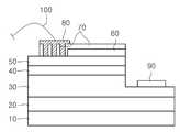
도 1을 참조하면, 발광 소자는 성장 기판(10) 상에 형성된 버퍼층을 포함하는 언도프트(Un-doped) 질화물층(20)과, 상기 언도프트 질화물층(20) 상에 형성된 제1 도전형의 반도체층(30), 활성층(40), 및 제2 도전형의 반도체층(50)을 포함하는 발광 구조층과, 상기 제2 도전형의 반도체층(50) 상에 형성된 투명 전극층(60)과, 상기 제1 도전형의 반도체층(30) 상에 형성된 제1 전극층(90)과, 상기 투명 전극층(60) 상에 형성된 제2 전극층(70)과, 상기 제2 전극층(70) 상에 형성된 전극 패드(80)를 포함한다.Referring to FIG. 1, the light emitting device includes an
상기 성장 기판(10)은 사파이어(Al2O3), Si, SiC, GaAs, ZnO, MgO 중 어느 하나로 형성될 수 있고, 예를 들어, 상기 성장 기판(10)으로서 사파이어 기판을 사용할 수 있다.The
상기 언도프트 질화물층(20)은 GaN계 반도체층으로 형성될 수 있고, 예를 들어, 트리메틸 갈륨(TMGa)을 수소 가스 및 암모니아 가스와 함께 챔버에 주입하여 성장시킨 언도프트 GaN층을 사용할 수 있다.The
상기 제1 도전형의 반도체층(30)은 트리메틸 갈륨(TMGa), n형 불순물(예를 들어, Si)을 포함하는 실란 가스(SiH4)를 수소 가스 및 암모니아 가스와 함께 상기 챔버에 주입하여 성장시킬 수 있다. 그리고, 상기 제1 도전형의 반도체층(30) 상에 활성층(40) 및 제2 도전형의 반도체층(50)을 형성한다.The first
상기 활성층(40)은 단일 양자 우물 구조 또는 다중 양자 우물 구조로 형성될 수 있고, 예를 들어, InGaN 우물층/GaN 장벽층의 적층 구조로 형성될 수도 있다.The
상기 제2 도전형의 반도체층(50)은 트리메틸 갈륨(TMGa), p형 불순물(예를 들어, Mg)을 포함하는 비세틸 사이클로 펜타니에닐 마그네슘(EtCp2Mg){Mg(C2H5C5H4)2}을 수소 가스 및 암모니아 가스와 함께 상기 챔버에 주입하여 성장시킬 수 있다.The second
상기 투명 전극층(60)은 상기 제2 도전형의 반도체층(50)과 상기 제2 전극층(70) 사이에 배치되어 오믹 접촉층의 역할을 하며, 예를 들어, ITO, ZnO, RuOx, TiOx, 또는 IrOx 중 적어도 어느 하나로 형성될 수도 있다.The
상기 제2 전극층(70)은 소정 형태의 패턴으로 형성될 수 있으며, 상기 제2 전극층(70) 상에 전극 패드(80)가 형성된다. 상기 제2 전극층(70)의 패턴에 대해서는 후술하도록 한다.The
또한, 실시예에서는 제2 전극층(70)이 소정 형태의 패턴으로 형성되고, 상기 제2 전극층(70) 상에 전극 패드(80)가 형성되며, 상기 전극 패드(80)가 와이어(100)를 통해 외부 전원과 연결된 것이 개시되어 있으나, 이와 같은 구조는 상기 제1 전극층(90)에도 적용될 수 있다.In addition, in the exemplary embodiment, the
실시예에서는 상기 제2 전극층(70)이 소정 패턴을 갖도록 함으로써, 상기 전극 패드(80)의 일부는 상기 투명 전극층(60)과 접촉하고 상기 전극 패드(80)의 일부는 상기 제2 전극층(70)과 접촉한다.In the embodiment, the
상기 제2 전극층(70)의 패턴에 의해 상기 전극 패드(80)과 상기 제2 전극층(70)은 접합 면적이 증가되기 때문에, 상기 전극 패드(80)와 상기 제2 전극층(70) 사이의 결합력이 증가될 수 있다.Since the bonding area of the
도 2에 도시된 발광 소자는 도 1에 도시된 발광 소자와 유사한 구조를 갖는다. 따라서, 도 1의 발광 소자에 대한 설명과 중복되는 설명은 생략하도록 한다.The light emitting device shown in FIG. 2 has a structure similar to the light emitting device shown in FIG. 1. Therefore, a description overlapping with the description of the light emitting device of FIG. 1 will be omitted.
도 2를 참조하면, 상기 제2 도전형의 반도체층(50) 상에 부분적으로 상기 투명 전극층(60)이 형성되고, 상기 제2 전극층(70)은 상기 제2 도전형의 반도체층(50) 및 상기 투명 전극층(60) 상에 형성된다.Referring to FIG. 2, the
상기 제2 전극층(70)은 소정 패턴을 갖고, 상기 제2 전극층(70)의 패턴에 의해 상기 제2 도전형의 반도체층(50)이 부분적으로 상측 방향으로 노출된다. 상기 제2 전극층(70) 상에는 전극 패드(80)가 형성되는데, 상기 전극 패드(80)의 일부는 상기 제2 도전형의 반도체층(50)과 접합한다.The
상기 제2 전극층(70)의 패턴에 의해 상기 제2 전극층(70)과 전극 패드(80)의 접합 면적이 증가되기 때문에, 상기 전극 패드(80)와 상기 제2 전극층(70) 사이의 결합력이 증가될 수 있다.Since the bonding area of the
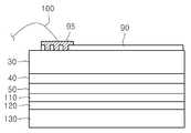
도 3에 도시된 발광 소자는 도 1 및 도 2에 도시된 수평형 타입의 발광 소자와 달리 수직형 타입의 발광 소자가 예시되어 있다.In the light emitting device shown in FIG. 3, a vertical type light emitting device is illustrated, unlike the light emitting device of the horizontal type shown in FIGS. 1 and 2.
도 3을 참조하면, 발광 소자는 전도성 지지기판(130) 상에 반사층(120)과, 상기 반사층(120) 상에 오믹 접촉층(110)과, 상기 오믹 접촉층(110) 상에 제2 도전형의 반도체층(50)과, 상기 제2 도전형의 반도체층(50) 상에 활성층(40)과, 상기 활성층(40) 상에 제1 도전형의 반도체층(30)과, 상기 제1 도전형의 반도체층(30) 상에 제1 전극층(90)과, 상기 제1 전극층(90) 상에 전극 패드(95)를 포함한다.Referring to FIG. 3, the light emitting device includes a
상기 제1 전극층(90)은 소정 패턴을 갖고 상기 패턴에 의해 상기 제1 도전형의 반도체층(30)의 일부가 부분적으로 상측 방향으로 노출된다. 상기 제1 전극층(90) 상에는 와이어(100)와 연결된 상기 전극 패드(95)가 형성되는데, 상기 전극 패드(95)의 일부는 상기 제1 도전형의 반도체층(30)과 접합한다.The
상기 제1 전극층(90)의 패턴에 의해 상기 제1 전극층(90)과 전극 패드(95)의 접합 면적이 증가되기 때문에, 상기 전극 패드(95)와 상기 제1 전극층(90) 사이의 결합력이 증가될 수 있다.Since the bonding area of the
도 1 내지 도 3에 도시된 바와 같이, 실시예에 따른 발광 소자에는 전원을 인가하기 위한 전극층이 형성되는데, 상기 전극층은 전극 패드와의 결합력을 증가시키기 위해 소정 패턴으로 형성된다.1 to 3, the light emitting device according to the embodiment is formed with an electrode layer for applying power, the electrode layer is formed in a predetermined pattern to increase the bonding force with the electrode pad.
도 4는 제1 실시예에 따른 발광 소자의 전극층을 도시한 도면이다.4 is a diagram illustrating an electrode layer of a light emitting device according to the first embodiment.
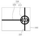
도 4를 참조하면, 도전층(200) 상에 패드부(210)와 핑거부(220)를 포함하는 전극층(230)이 형성된다.Referring to FIG. 4, an
상기 도전층(200)은 발광 소자의 제1 도전형의 반도체층 또는 제2 도전형의 반도체층에 전원을 제공하기 위한 층이 될 수 있다. 즉, 상기 도전층(200)은 상기 발광 구조층의 일부이거나 상기 발광 구조층과 전기적으로 연결된 층이 될 수 있다. 예를 들어, 상기 도전층(200)은 제1 도전형의 반도체층, 제2 도전형의 반도체층, 또는 투명 전극층 중 어느 하나가 될 수 있다.The
상기 패드부(210)는 대략 원판 형태 패턴을 포함하고, 상기 핑거부(220)는 상기 패드부(210)와 연결되어 상기 패드부(210)로부터 선형으로 연장되는 패턴을 포함한다. 상기 패드부(210)에는 적어도 하나의 개구(219)가 형성되어 상기 개구(219)를 통해 상기 도전층(200)이 상측 방향으로 노출된다. 실시예에는 복수개의 개구(219)가 상기 패드부(210) 내에 형성된 것이 개시되어 있다.The
도 1 내지 도 3에 도시된 바와 같이, 상기 패드부(210) 상에는 전극 패드가 형성되는데, 상기 패드부(210)의 패턴에 의해 상기 전극 패드는 상기 패드부(210)와 접합되는 면적이 증가되어 결합력이 향상된다.As illustrated in FIGS. 1 to 3, an electrode pad is formed on the
도 5는 제2 실시예에 따른 발광 소자의 전극층을 도시한 도면이다.5 is a diagram illustrating an electrode layer of a light emitting device according to a second embodiment.
제2 실시예를 설명함에 있어서 상술한 제1 실시예와 중복되는 설명은 생략하도록 한다.In the description of the second embodiment, a description overlapping with the above-described first embodiment will be omitted.
도 5를 참조하면, 도전층(200) 상에 패드부(210)와 핑거부(220)를 포함하는 전극층(230)이 형성된다.Referring to FIG. 5, an
상기 패드부(210)는 대략 원판 형태의 패턴을 포함하고, 상기 핑거부(220)는 상기 패드부(210)와 이격되고 선형으로 연장되는 패턴을 포함한다. 상기 핑거부(220)와 패드부(210)는 상기 도전층(200)을 통해 전기적으로 연결된다. 상기 패드부(210)에는 다수의 개구(219)가 형성되어 상기 개구(219)를 통해 상기 도전 층(200)이 상측 방향으로 노출된다.The
도 1 내지 도 3에 도시된 바와 같이, 상기 패드부(210) 상에는 전극 패드가 형성되는데, 상기 패드부(210)의 패턴에 의해 상기 전극 패드는 상기 패드부(210)와 접합되는 면적이 증가되어 결합력이 향상된다.As illustrated in FIGS. 1 to 3, an electrode pad is formed on the
도 6은 제3 실시예에 따른 발광 소자의 전극층을 도시한 도면이다.6 is a diagram illustrating an electrode layer of a light emitting device according to a third embodiment.
제3 실시예를 설명함에 있어서 상술한 제1 실시예와 중복되는 설명은 생략하도록 한다.In the description of the third embodiment, a description overlapping with the first embodiment will be omitted.
도 6을 참조하면, 도전층(200) 상에 패드부(210)와 핑거부(220)를 포함하는 전극층(230)이 형성된다.Referring to FIG. 6, an
상기 패드부(210)는 동심원 형태의 패턴을 포함하고, 상기 핑거부(220)는 상기 패드부(210)와 연결되고 상기 패드부(210)로부터 선형으로 연장되는 패턴을 포함한다. 상기 패드부(210)는 서로 연결된 다수의 동심원 형태의 패턴이 배치된 형태로 형성되고, 상기 패드부(210)와 상기 핑거부(220)는 패턴의 선폭이 동일한 층으로 형성된다.The
상기 패드부(210)에는 다수의 동심원 형태의 패턴 사이에 개구가 형성되어 상기 개구를 통해 상기 도전층(200)이 상측 방향으로 노출된다.An opening is formed in the
도 1 내지 도 3에 도시된 바와 같이, 상기 패드부(210) 상에는 전극 패드가 형성되는데, 상기 패드부(210)의 패턴에 의해 상기 전극 패드는 상기 패드부(210)와 접합되는 면적이 증가되어 결합력이 향상된다.As illustrated in FIGS. 1 to 3, an electrode pad is formed on the
도 7은 제4 실시예에 따른 발광 소자의 전극층을 도시한 도면이다.7 is a diagram illustrating an electrode layer of a light emitting device according to a fourth embodiment.
제4 실시예를 설명함에 있어서 상술한 제1 실시예와 중복되는 설명은 생략하도록 한다.In the description of the fourth embodiment, description overlapping with the above-described first embodiment will be omitted.
도 7을 참조하면, 도전층(200) 상에 패드부(210)와 핑거부(220)를 포함하는 전극층(230)이 형성된다.Referring to FIG. 7, an
상기 패드부(210)는 원판 형태의 패턴과 동심원 형태의 패턴을 포함하고, 상기 핑거부(220)는 상기 패드부(210)와 연결되고 상기 패드부(210)로부터 선형으로 연장되는 패턴을 포함한다. 상기 패드부(210)는 서로 이격된 다수의 동심원 형태의 패턴이 배치되고, 상기 패드부(210)의 적어도 일부와 상기 핑거부(220)는 패턴의 선폭이 동일한 층으로 형성된다.The
상기 패드부(210)에는 원판 형태의 패턴과 동심원 패턴 사이에 개구가 형성되어 상기 개구를 통해 상기 도전층(200)이 상측 방향으로 노출된다.An opening is formed in the
도 1 내지 도 3에 도시된 바와 같이, 상기 패드부(210) 상에는 전극 패드가 형성되는데, 상기 패드부(210)의 패턴에 의해 상기 전극 패드는 상기 패드부(210)와 접합되는 면적이 증가되어 결합력이 향상된다.As illustrated in FIGS. 1 to 3, an electrode pad is formed on the
도 8은 제5 실시예에 따른 발광 소자의 전극층을 도시한 도면이다.8 is a diagram illustrating an electrode layer of a light emitting device according to a fifth embodiment.
제5 실시예를 설명함에 있어서 상술한 제1 실시예와 중복되는 설명은 생략하도록 한다.In the description of the fifth embodiment, a description overlapping with the first embodiment will be omitted.
도 8을 참조하면, 도전층(200) 상에 패드부(210)와 핑거부(220)를 포함하는 전극층(230)이 형성된다.Referring to FIG. 8, an
상기 패드부(210)는 대략 원판 형태의 패턴과 동심원 형태의 패턴을 포함하 고, 상기 핑거부(220)는 상기 패드부(210)와 연결되고 상기 패드부(210)로부터 선형으로 연장되는 패턴을 포함한다. 상기 패드부(210)는 일부가 서로 연결된 다수의 동심원 패턴과 원판 형태의 패턴이 배치되고, 상기 패드부(210)의 적어도 일부와 상기 핑거부(220)는 패턴의 선폭이 동일한 층으로 형성된다.The
상기 패드부(210)에는 다수의 동심원 패턴과 원판 형태의 패턴 사이에 개구가 형성되어 상기 개구를 통해 상기 도전층(200)이 상측 방향으로 노출된다.An opening is formed in the
도 1 내지 도 3에 도시된 바와 같이, 상기 패드부(210) 상에는 전극 패드가 형성되는데, 상기 패드부(210)의 패턴에 의해 상기 전극 패드는 상기 패드부(210)와 접합되는 면적이 증가되어 결합력이 향상된다.As illustrated in FIGS. 1 to 3, an electrode pad is formed on the
도 9는 제6 실시예에 따른 발광 소자의 전극층을 도시한 도면이다.9 is a diagram illustrating an electrode layer of a light emitting device according to a sixth embodiment.
제6 실시예를 설명함에 있어서 상술한 제1 실시예와 중복되는 설명은 생략하도록 한다.In describing the sixth embodiment, a description overlapping with the above-described first embodiment will be omitted.
도 9를 참조하면, 도전층(200) 상에 패드부(210)와 핑거부(220)를 포함하는 전극층(230)이 형성된다.Referring to FIG. 9, an
상기 패드부(210)는 대략 원형의 패턴을 포함하고, 상기 핑거부(220)는 상기 패드부(210)와 연결되고 상기 패드부(210)로부터 선형으로 연장되는 패턴을 포함한다. 상기 패드부(210)는 원형의 패턴이 배치되고, 일부분이 원형의 패턴 내부로 연장된다.The
상기 패드부(210)의 적어도 일부와 상기 핑거부(220)는 패턴의 선폭이 동일한 층으로 형성된다.At least a portion of the
상기 패드부(210)에는 원형의 패턴 내부에 개구가 형성되어 상기 개구를 통해 상기 도전층(200)이 상측 방향으로 노출된다.An opening is formed in a circular pattern in the
도 1 내지 도 3에 도시된 바와 같이, 상기 패드부(210) 상에는 전극 패드가 형성되는데, 상기 패드부(210)의 패턴에 의해 상기 전극 패드는 상기 패드부(210)와 접합되는 면적이 증가되어 결합력이 향상된다.As illustrated in FIGS. 1 to 3, an electrode pad is formed on the
도 10은 제7 실시예에 따른 발광 소자의 전극층을 도시한 도면이다.10 is a view showing an electrode layer of a light emitting device according to a seventh embodiment.
제7 실시예를 설명함에 있어서 상술한 제1 실시예와 중복되는 설명은 생략하도록 한다.In describing the seventh embodiment, a description overlapping with the above-described first embodiment will be omitted.
도 10을 참조하면, 도전층(200) 상에 패드부(210)와 핑거부(220)를 포함하는 전극층(230)이 형성된다.Referring to FIG. 10, an
상기 패드부(210)는 복수의 서로 이격된 패턴을 포함하고, 상기 패턴 중 적어도 일부는 호형의 패턴을 포함한다. 상기 핑거부(220)는 상기 패드부(210)와 연결되고 상기 패드부(210)로부터 선형으로 연장되는 패턴을 포함한다.The
상기 핑거부(220)들에 각각 연결된 패드부(210)들은 서로 분리되어 형성된다. 또한, 상기 패드부(210)와 상기 핑거부(220)는 패턴의 선폭이 동일한 층으로 형성된다.
도 1 내지 도 3에 도시된 바와 같이, 상기 패드부(210) 상에는 전극 패드가 형성되는데, 상기 패드부(210)의 패턴에 의해 상기 전극 패드는 상기 패드부(210)와 접합되는 면적이 증가되어 결합력이 향상된다.As illustrated in FIGS. 1 to 3, an electrode pad is formed on the
도 11은 제8 실시예에 따른 발광 소자의 전극층을 도시한 도면이다.11 is a view showing an electrode layer of the light emitting device according to the eighth embodiment.
제8 실시예를 설명함에 있어서 상술한 제1 실시예와 중복되는 설명은 생략하도록 한다.In describing the eighth embodiment, a description overlapping with the above-described first embodiment will be omitted.
도 11을 참조하면, 도전층(200) 상에 패드부(210)와 핑거부(220)를 포함하는 전극층(230)이 형성된다.Referring to FIG. 11, an
상기 패드부(210)는 나선 형태의 패턴을 포함하고, 상기 핑거부(220)는 상기 패드부(210)와 연결되고 상기 패드부(210)로부터 선형으로 연장되는 패턴을 포함한다. 또한, 상기 패드부(210)와 상기 핑거부(220)는 패턴의 선폭이 동일한 층으로 형성된다.The
도 1 내지 도 3에 도시된 바와 같이, 상기 패드부(210) 상에는 전극 패드가 형성되는데, 상기 패드부(210)의 패턴에 의해 상기 전극 패드는 상기 패드부(210)와 접합되는 면적이 증가되어 결합력이 향상된다.As illustrated in FIGS. 1 to 3, an electrode pad is formed on the
이상에서 실시예들에 설명된 특징, 구조, 효과 등은 본 발명의 적어도 하나의 실시예에 포함되며, 반드시 하나의 실시예에만 한정되는 것은 아니다. 나아가, 각 실시예에서 예시된 특징, 구조, 효과 등은 실시예들이 속하는 분야의 통상의 지식을 가지는 자에 의해 다른 실시예들에 대해서도 조합 또는 변형되어 실시 가능하다. 따라서 이러한 조합과 변형에 관계된 내용들은 본 발명의 범위에 포함되는 것으로 해석되어야 할 것이다.Features, structures, effects, and the like described in the above embodiments are included in at least one embodiment of the present invention, and are not necessarily limited to only one embodiment. Furthermore, the features, structures, effects, and the like illustrated in the embodiments may be combined or modified with respect to other embodiments by those skilled in the art to which the embodiments belong. Therefore, it should be understood that the present invention is not limited to these combinations and modifications.
이상에서 실시예를 중심으로 설명하였으나 이는 단지 예시일 뿐 본 발명을 한정하는 것이 아니며, 본 발명이 속하는 분야의 통상의 지식을 가진 자라면 본 실시예의 본질적인 특성을 벗어나지 않는 범위에서 이상에 예시되지 않은 여러 가지 의 변형과 응용이 가능함을 알 수 있을 것이다. 예를 들어, 실시예에 구체적으로 나타난 각 구성 요소는 변형하여 실시할 수 있는 것이다. 그리고 이러한 변형과 응용에 관계된 차이점들은 첨부된 청구 범위에서 규정하는 본 발명의 범위에 포함되는 것으로 해석되어야 할 것이다.Although the above description has been made based on the embodiments, these are merely examples and are not intended to limit the present invention. Those skilled in the art to which the present invention pertains may not have been exemplified above without departing from the essential characteristics of the present embodiments. It will be appreciated that many variations and applications are possible. For example, each component specifically shown in the embodiment can be modified. And differences relating to such modifications and applications will have to be construed as being included in the scope of the invention defined in the appended claims.
도 1 내지 도 3은 실시예들에 따른 발광 소자를 설명하는 도면.1 to 3 illustrate light emitting devices according to embodiments.
도 4는 제1 실시예에 따른 발광 소자의 전극층을 도시한 도면.4 is a view showing an electrode layer of a light emitting device according to the first embodiment;
도 5는 제2 실시예에 따른 발광 소자의 전극층을 도시한 도면.5 is a view showing an electrode layer of a light emitting device according to a second embodiment;
도 6은 제3 실시예에 따른 발광 소자의 전극층을 도시한 도면.6 is a view showing an electrode layer of a light emitting device according to a third embodiment;
도 7은 제4 실시예에 따른 발광 소자의 전극층을 도시한 도면.7 is a view showing an electrode layer of a light emitting device according to a fourth embodiment.
도 8은 제5 실시예에 따른 발광 소자의 전극층을 도시한 도면.8 illustrates an electrode layer of a light emitting device according to a fifth embodiment;
도 9는 제6 실시예에 따른 발광 소자의 전극층을 도시한 도면.9 illustrates an electrode layer of a light emitting device according to a sixth embodiment;
도 10은 제7 실시예에 따른 발광 소자의 전극층을 도시한 도면.10 illustrates an electrode layer of a light emitting device according to a seventh embodiment;
도 11은 제8 실시예에 따른 발광 소자의 전극층을 도시한 도면.11 is a view showing an electrode layer of a light emitting device according to an eighth embodiment;
Claims (13)
Translated fromKoreanPriority Applications (4)
| Application Number | Priority Date | Filing Date | Title |
|---|---|---|---|
| KR1020090123005AKR100974777B1 (en) | 2009-12-11 | 2009-12-11 | A light emitting device |
| EP10193876.9AEP2333851B1 (en) | 2009-12-11 | 2010-12-06 | Light emitting device, light emitting device package, and lighting system |
| US12/964,454US8053805B2 (en) | 2009-12-11 | 2010-12-09 | Light emitting device, light emitting device and package, and lighting system |
| CN201010599378.XACN102130257B (en) | 2009-12-11 | 2010-12-13 | Light emitting device, light emitting device package, and lighting system |
Applications Claiming Priority (1)
| Application Number | Priority Date | Filing Date | Title |
|---|---|---|---|
| KR1020090123005AKR100974777B1 (en) | 2009-12-11 | 2009-12-11 | A light emitting device |
Publications (1)
| Publication Number | Publication Date |
|---|---|
| KR100974777B1true KR100974777B1 (en) | 2010-08-06 |
Family
ID=42759417
Family Applications (1)
| Application Number | Title | Priority Date | Filing Date |
|---|---|---|---|
| KR1020090123005AExpired - Fee RelatedKR100974777B1 (en) | 2009-12-11 | 2009-12-11 | A light emitting device |
Country Status (4)
| Country | Link |
|---|---|
| US (1) | US8053805B2 (en) |
| EP (1) | EP2333851B1 (en) |
| KR (1) | KR100974777B1 (en) |
| CN (1) | CN102130257B (en) |
Families Citing this family (9)
| Publication number | Priority date | Publication date | Assignee | Title |
|---|---|---|---|---|
| KR101786094B1 (en)* | 2011-06-23 | 2017-10-16 | 엘지이노텍 주식회사 | Light emitting device, light emitting device package, and light unit |
| US8564010B2 (en)* | 2011-08-04 | 2013-10-22 | Toshiba Techno Center Inc. | Distributed current blocking structures for light emitting diodes |
| JP5960426B2 (en)* | 2011-12-16 | 2016-08-02 | スタンレー電気株式会社 | Semiconductor device and method for manufacturing semiconductor device |
| KR102075992B1 (en) | 2013-10-17 | 2020-02-11 | 삼성전자주식회사 | Semiconductor Light Emitting Device |
| KR102070089B1 (en)* | 2013-10-23 | 2020-01-29 | 삼성전자주식회사 | Semiconductor light emitting diode package and lighting device using the same |
| CN103682023A (en)* | 2013-12-30 | 2014-03-26 | 杭州士兰明芯科技有限公司 | LED (Light Emitting Diode) structure and electrode formation method thereof |
| DE112015003973T5 (en)* | 2014-08-29 | 2017-06-22 | Hamamatsu Photonics K.K. | SURFACE-EMITTING LASER WITH TWO-DIMENSIONAL PHOTONIC CRYSTAL |
| US10938177B2 (en) | 2014-08-29 | 2021-03-02 | Kyoto University | Two-dimensional photonic crystal surface emitting laser |
| WO2021174412A1 (en)* | 2020-03-03 | 2021-09-10 | 东莞市中麒光电技术有限公司 | Light-emitting diode and preparation method therefor |
Citations (4)
| Publication number | Priority date | Publication date | Assignee | Title |
|---|---|---|---|---|
| KR20040008092A (en)* | 2002-07-17 | 2004-01-28 | 스미토모덴키고교가부시키가이샤 | Structure of p-electrode at the light-emerging side of light-emitting diode |
| KR100452751B1 (en) | 2003-06-03 | 2004-10-15 | 삼성전기주식회사 | III-Nitride compound semiconductor light emitting device with mesh type electrode |
| KR100765903B1 (en) | 2007-03-13 | 2007-10-10 | (주)에피플러스 | Light Emitting Diodes With Current Dispersion Holes |
| KR20080042340A (en)* | 2006-11-09 | 2008-05-15 | 서울옵토디바이스주식회사 | Light Emitting Diode with Uniform Current Density |
Family Cites Families (24)
| Publication number | Priority date | Publication date | Assignee | Title |
|---|---|---|---|---|
| JPH05303106A (en)* | 1992-04-27 | 1993-11-16 | Sanyo Electric Co Ltd | Liquid crystal display device |
| TW329500B (en)* | 1995-11-14 | 1998-04-11 | Handotai Energy Kenkyusho Kk | Electro-optical device |
| JP2000174339A (en)* | 1998-12-04 | 2000-06-23 | Mitsubishi Cable Ind Ltd | GaN based semiconductor light emitting device and GaN based semiconductor light receiving device |
| TW516248B (en)* | 2001-12-21 | 2003-01-01 | Epitech Technology Corp | Nitride light emitting diode with spiral-shaped metal electrode |
| US6599768B1 (en)* | 2002-08-20 | 2003-07-29 | United Epitaxy Co., Ltd. | Surface mounting method for high power light emitting diode |
| US6958498B2 (en)* | 2002-09-27 | 2005-10-25 | Emcore Corporation | Optimized contact design for flip-chip LED |
| US7202928B2 (en)* | 2003-10-16 | 2007-04-10 | Lg. Philips Lcd Co., Ltd | Array substrate for in-plane switching mode liquid crystal display device and method of fabricating the same |
| US7160741B2 (en)* | 2003-11-06 | 2007-01-09 | Chartered Semiconductor Manufacturing Ltd. | Planar voltage contrast test structure and method |
| TWI234298B (en)* | 2003-11-18 | 2005-06-11 | Itswell Co Ltd | Semiconductor light emitting diode and method for manufacturing the same |
| US7227607B2 (en)* | 2003-12-11 | 2007-06-05 | Lg.Philips Lcd Co., Ltd | Array substrate for in-plane switching mode liquid crystal display device and method of fabricating the same |
| KR100603829B1 (en)* | 2003-12-12 | 2006-07-24 | 엘지.필립스 엘시디 주식회사 | Fringe field switching mode LCD |
| US20050161779A1 (en)* | 2004-01-26 | 2005-07-28 | Hui Peng | Flip chip assemblies and lamps of high power GaN LEDs, wafer level flip chip package process, and method of fabricating the same |
| JP2005244207A (en)* | 2004-01-30 | 2005-09-08 | Showa Denko Kk | Gallium nitride compound semiconductor light emitting device |
| JP4907121B2 (en)* | 2005-07-28 | 2012-03-28 | 昭和電工株式会社 | Light emitting diode and light emitting diode lamp |
| KR100616693B1 (en)* | 2005-08-09 | 2006-08-28 | 삼성전기주식회사 | Nitride semiconductor light emitting device |
| JP4947954B2 (en)* | 2005-10-31 | 2012-06-06 | スタンレー電気株式会社 | Light emitting element |
| EP1887634A3 (en)* | 2006-08-11 | 2011-09-07 | OSRAM Opto Semiconductors GmbH | Semiconductor light emitting device |
| US7714340B2 (en)* | 2006-09-06 | 2010-05-11 | Palo Alto Research Center Incorporated | Nitride light-emitting device |
| US8222714B2 (en)* | 2007-02-05 | 2012-07-17 | Rambus Inc. | Semiconductor package with embedded spiral inductor |
| TWI475716B (en)* | 2007-03-19 | 2015-03-01 | Epistar Corp | Optoelectronic component |
| TWI362530B (en)* | 2008-02-26 | 2012-04-21 | Au Optronics Corp | Pixel unit, liquid crystal display panel, electro-optical apparatus, and methods of manufacturing the same |
| US7935979B2 (en)* | 2008-05-01 | 2011-05-03 | Bridgelux, Inc. | Wire bonding to connect electrodes |
| CN101290446B (en)* | 2008-05-16 | 2011-10-05 | 京东方科技集团股份有限公司 | TFT-LCD array substrate and manufacturing method thereof |
| US20100295088A1 (en)* | 2008-10-02 | 2010-11-25 | Soraa, Inc. | Textured-surface light emitting diode and method of manufacture |
- 2009
- 2009-12-11KRKR1020090123005Apatent/KR100974777B1/ennot_activeExpired - Fee Related
- 2010
- 2010-12-06EPEP10193876.9Apatent/EP2333851B1/ennot_activeNot-in-force
- 2010-12-09USUS12/964,454patent/US8053805B2/ennot_activeExpired - Fee Related
- 2010-12-13CNCN201010599378.XApatent/CN102130257B/ennot_activeExpired - Fee Related
Patent Citations (4)
| Publication number | Priority date | Publication date | Assignee | Title |
|---|---|---|---|---|
| KR20040008092A (en)* | 2002-07-17 | 2004-01-28 | 스미토모덴키고교가부시키가이샤 | Structure of p-electrode at the light-emerging side of light-emitting diode |
| KR100452751B1 (en) | 2003-06-03 | 2004-10-15 | 삼성전기주식회사 | III-Nitride compound semiconductor light emitting device with mesh type electrode |
| KR20080042340A (en)* | 2006-11-09 | 2008-05-15 | 서울옵토디바이스주식회사 | Light Emitting Diode with Uniform Current Density |
| KR100765903B1 (en) | 2007-03-13 | 2007-10-10 | (주)에피플러스 | Light Emitting Diodes With Current Dispersion Holes |
Also Published As
| Publication number | Publication date |
|---|---|
| EP2333851B1 (en) | 2019-02-13 |
| US20110140161A1 (en) | 2011-06-16 |
| US8053805B2 (en) | 2011-11-08 |
| CN102130257A (en) | 2011-07-20 |
| CN102130257B (en) | 2015-06-17 |
| EP2333851A2 (en) | 2011-06-15 |
| EP2333851A3 (en) | 2014-04-09 |
Similar Documents
| Publication | Publication Date | Title |
|---|---|---|
| KR100974777B1 (en) | A light emitting device | |
| KR101761385B1 (en) | Light emitting device | |
| KR100969100B1 (en) | Light emitting device, manufacturing method and light emitting device package | |
| CN103078032B (en) | Light emitting device | |
| KR101114782B1 (en) | Light emitting device, light emitting device package and method for fabricating the same | |
| CN105576108B (en) | light emitting device | |
| JP5379116B2 (en) | Light emitting device, light emitting device package, and lighting system | |
| KR101276053B1 (en) | Semiconductor light emitting device and light emitting apparatus | |
| KR20130046755A (en) | Light emitting device | |
| KR20150002113A (en) | Light emitting device, light emitting device package and apparatus for driving a light emitting device | |
| JP2011129922A (en) | Light emitting element, light emitting element manufacturing method, light emitting element package, and lighting system | |
| CN104025296A (en) | Optoelectronic semiconductor chip and method for the production thereof | |
| KR100999800B1 (en) | Light emitting device package and its manufacturing method | |
| KR101039880B1 (en) | Light emitting device and light emitting device package | |
| CN102194936B (en) | Light emitting device, light emitting device package, and lighting system | |
| KR101710358B1 (en) | Light Emitting diode and Light Emitting diode Package | |
| KR101039931B1 (en) | Light emitting device and manufacturing method | |
| KR101125416B1 (en) | Light emitting device, method for fabricating the light emitting device and light emitting device package | |
| KR101661621B1 (en) | Substrate formed pattern and light emitting device | |
| KR101628384B1 (en) | Light emitting device, method for fabricating the light emitting device and light emitting device package | |
| KR20160059221A (en) | Light emitting device and lighting system | |
| KR102008349B1 (en) | Light emitting device and light emitting device package | |
| KR102075059B1 (en) | Light emitting device and light emitting device package | |
| KR20120006348A (en) | Light emitting element | |
| KR20120052746A (en) | Light emitting device |
Legal Events
| Date | Code | Title | Description |
|---|---|---|---|
| A201 | Request for examination | ||
| PA0109 | Patent application | St.27 status event code:A-0-1-A10-A12-nap-PA0109 | |
| PA0201 | Request for examination | St.27 status event code:A-1-2-D10-D11-exm-PA0201 | |
| R18-X000 | Changes to party contact information recorded | St.27 status event code:A-3-3-R10-R18-oth-X000 | |
| A302 | Request for accelerated examination | ||
| PA0302 | Request for accelerated examination | St.27 status event code:A-1-2-D10-D17-exm-PA0302 St.27 status event code:A-1-2-D10-D16-exm-PA0302 | |
| D13-X000 | Search requested | St.27 status event code:A-1-2-D10-D13-srh-X000 | |
| D14-X000 | Search report completed | St.27 status event code:A-1-2-D10-D14-srh-X000 | |
| E701 | Decision to grant or registration of patent right | ||
| PE0701 | Decision of registration | St.27 status event code:A-1-2-D10-D22-exm-PE0701 | |
| GRNT | Written decision to grant | ||
| PR0701 | Registration of establishment | St.27 status event code:A-2-4-F10-F11-exm-PR0701 | |
| PR1002 | Payment of registration fee | St.27 status event code:A-2-2-U10-U11-oth-PR1002 Fee payment year number:1 | |
| PG1601 | Publication of registration | St.27 status event code:A-4-4-Q10-Q13-nap-PG1601 | |
| FPAY | Annual fee payment | Payment date:20130705 Year of fee payment:4 | |
| PR1001 | Payment of annual fee | St.27 status event code:A-4-4-U10-U11-oth-PR1001 Fee payment year number:4 | |
| FPAY | Annual fee payment | Payment date:20140708 Year of fee payment:5 | |
| PR1001 | Payment of annual fee | St.27 status event code:A-4-4-U10-U11-oth-PR1001 Fee payment year number:5 | |
| PN2301 | Change of applicant | St.27 status event code:A-5-5-R10-R13-asn-PN2301 St.27 status event code:A-5-5-R10-R11-asn-PN2301 | |
| FPAY | Annual fee payment | Payment date:20150706 Year of fee payment:6 | |
| PR1001 | Payment of annual fee | St.27 status event code:A-4-4-U10-U11-oth-PR1001 Fee payment year number:6 | |
| FPAY | Annual fee payment | Payment date:20160707 Year of fee payment:7 | |
| PR1001 | Payment of annual fee | St.27 status event code:A-4-4-U10-U11-oth-PR1001 Fee payment year number:7 | |
| R18-X000 | Changes to party contact information recorded | St.27 status event code:A-5-5-R10-R18-oth-X000 | |
| FPAY | Annual fee payment | Payment date:20170704 Year of fee payment:8 | |
| PR1001 | Payment of annual fee | St.27 status event code:A-4-4-U10-U11-oth-PR1001 Fee payment year number:8 | |
| FPAY | Annual fee payment | Payment date:20180710 Year of fee payment:9 | |
| PR1001 | Payment of annual fee | St.27 status event code:A-4-4-U10-U11-oth-PR1001 Fee payment year number:9 | |
| R18-X000 | Changes to party contact information recorded | St.27 status event code:A-5-5-R10-R18-oth-X000 | |
| FPAY | Annual fee payment | Payment date:20190711 Year of fee payment:10 | |
| PR1001 | Payment of annual fee | St.27 status event code:A-4-4-U10-U11-oth-PR1001 Fee payment year number:10 | |
| R18-X000 | Changes to party contact information recorded | St.27 status event code:A-5-5-R10-R18-oth-X000 | |
| PR1001 | Payment of annual fee | St.27 status event code:A-4-4-U10-U11-oth-PR1001 Fee payment year number:11 | |
| PN2301 | Change of applicant | St.27 status event code:A-5-5-R10-R13-asn-PN2301 St.27 status event code:A-5-5-R10-R11-asn-PN2301 | |
| PN2301 | Change of applicant | St.27 status event code:A-5-5-R10-R11-asn-PN2301 | |
| PN2301 | Change of applicant | St.27 status event code:A-5-5-R10-R14-asn-PN2301 | |
| PR1001 | Payment of annual fee | St.27 status event code:A-4-4-U10-U11-oth-PR1001 Fee payment year number:12 | |
| PR1001 | Payment of annual fee | St.27 status event code:A-4-4-U10-U11-oth-PR1001 Fee payment year number:13 | |
| PC1903 | Unpaid annual fee | St.27 status event code:A-4-4-U10-U13-oth-PC1903 Not in force date:20230803 Payment event data comment text:Termination Category : DEFAULT_OF_REGISTRATION_FEE | |
| PC1903 | Unpaid annual fee | St.27 status event code:N-4-6-H10-H13-oth-PC1903 Ip right cessation event data comment text:Termination Category : DEFAULT_OF_REGISTRATION_FEE Not in force date:20230803 | |
| P22-X000 | Classification modified | St.27 status event code:A-4-4-P10-P22-nap-X000 |