KR100974604B1 - Electronic component package and manufacturing method thereof - Google Patents
Electronic component package and manufacturing method thereofDownload PDFInfo
- Publication number
- KR100974604B1 KR100974604B1KR1020080035172AKR20080035172AKR100974604B1KR 100974604 B1KR100974604 B1KR 100974604B1KR 1020080035172 AKR1020080035172 AKR 1020080035172AKR 20080035172 AKR20080035172 AKR 20080035172AKR 100974604 B1KR100974604 B1KR 100974604B1
- Authority
- KR
- South Korea
- Prior art keywords
- filler
- light emitting
- electronic component
- cavity
- package
- Prior art date
- Legal status (The legal status is an assumption and is not a legal conclusion. Google has not performed a legal analysis and makes no representation as to the accuracy of the status listed.)
- Active
Links
Images


Landscapes
- Led Device Packages (AREA)
Abstract
Translated fromKoreanDescription
Translated fromKorean본 발명은 전자부품 패키지 및 그의 제조방법에 관한 것으로, 보다 상세하게는 LED와 같은 발광소자를 채용한 전자부품 패키지 및 그의 제조방법에 관한 것이다.BACKGROUND OF THE
발광다이오드(light emission diode, 이하, LED라 함)는 GaAs, AlGaAs, GaN, InGaN 및 AlGaInP 등의 화합물 반도체(compound semiconductor) 재료의 변경을 통해 발광원을 구성함으로써 다양한 색을 구현할 수 있는 반도체 소자를 말한다. 현재, 이와 같은 반도체 소자가 전자부품에 패키지형태로 많이 채택되고 있다.A light emitting diode (hereinafter, referred to as an LED) is a semiconductor device capable of realizing various colors by configuring a light emitting source by changing compound semiconductor materials such as GaAs, AlGaAs, GaN, InGaN, and AlGaInP. Say. At present, many such semiconductor devices have been adopted in the form of packages in electronic components.
통상적으로, 반도체 패키지란 웨이퍼(Wafer)부터 소잉(Sawing)된 칩단위의 반도체 소자(예컨대, LED)을 서브스트레이트(Substrate)에 전기적으로 연결함과 동시에 수지 봉지재로 감싸서 마더보드(Mother Board)에 전기적으로 실장할 수 있는 형태의 것을 말한다.In general, a semiconductor package is a semiconductor board (eg, an LED) that is sawed from a wafer to a substrate, electrically connected to a substrate, and wrapped with a resin encapsulant, and being a mother board. It refers to a type that can be mounted electrically.
도 1을 참조하여 전형적인 램프형 LED와 표면실장형 LED의 각 패키지구조를 비교해 보면, 도 1의 (a)에 도시된 램프형 LED 패키지(10)인 경우에는 두 개의 리 드프레임(3a,3b) 중 하나의 리드프레임(3b)의 상부에는 컵형상으로 일정한 각을 갖는 금속 전극면이 구비되어 그 상부에 LED소자(5)가 실장되며, 또한, 투명 몰딩 수지류로 이루어진 반구형 케이스(7)에 의해 패키징되는 구조를 갖는다. 반면에 도 1의 (b)에 도시된 표면실장형 LED 패키지(20)는 몰딩 에폭시수지로 이루어진 패키지(11)를 가지며, 외형각이 적은 실장영역에 LED소자(15)가 배치되고 와이어(13)로 패턴 전극(미도시)과 연결되는 구조로 이루어진다.Referring to FIG. 1, a comparison of each package structure of a typical lamp type LED and a surface mounted LED is shown. In the case of the lamp
이와 같은 패키지 구조에 의해서, 램프형 LED 패키지(10)는 반구형의 케이스(7)가 렌즈역할을 한다. 특히, 휘도 분포를 좁게 조절하여 일정각에서 휘도를 높게 할 수 있고, 동시에 발광원으로부터 빛이 컵형인 금속 전극면에 의해 반사되어 휘도의 세기를 증대시킬 수 있다.With this package structure, the
이에 비해, 표면실장형 LED 패키지(20)에서는 패키지에 의해 넓은 휘도의 분포를 가지며, 그 휘도도 낮다. 이와 같이, 휘도는 패키지 구조에 의해 큰 영향을 받는다. 그에 따라, 세라믹기판을 이용한 내부실장 공간을 마련할 때에 발생되는 LED소자 주위의 수직 절개면 또는 경사진 캐비티에 각종 도금기술을 적용하거나 박편의 금속 반사판을 부착시킴으로서 휘도의 효율을 조금이라도 향상시키기 위한 발광다이오드 패키지(도 2참조)가 제안되었다.In contrast, in the surface-mount
즉, 도 2에 예시된 발광다이오드 패키지는, LED소자(105)의 실장영역(103)이 형성된 상면을 가지며, 실장영역(103)을 중심으로 소정의 도전성 패턴 전극이 형성된 제 1세라믹기판(101); 제 1세라믹기판(101) 상면의 실장영역(103)에 배치되어 와이어(107)에 의해 소정의 도전성 패턴 전극과 연결된 적어도 하나의 LED소 자(105); 제 1세라믹기판(101) 상에 배치되며 LED소자(105)의 실장영역(103)에 상응하는 영역에 캐비티가 형성된 제 2세라믹기판(102); 및 적어도 하나의 LED(105)소자를 둘러싸도록 제 2세라믹기판(102)의 캐비티내에 형성되고 그 상단에 제 2세라믹기판(102) 상단에 걸칠 수 있는 걸림턱(120a)이 형성된 금속 반사판(120)을 포함하여 구성된다.That is, the light emitting diode package illustrated in FIG. 2 has a top surface on which the
도 2의 발광다이오드 패키지는 금속 반사판(120)을 별도로 제작하여 부착시켜야 된다. 금속 반사판(120)을 사용함으로 인해 반사율을 높일 수 있지만, 금속 반사판(120)을 별도로 제작하는 별도 공정이 추가로 필요하다.The light emitting diode package of FIG. 2 should be manufactured by attaching the
그리고, 제작한 금속 반사판(120)을 일일이 수작업으로 제 2세라믹기판(102)의 캐비티내에 설치시켜야 되므로 시간이 많이 소요된다.In addition, since the manufactured
또한, 금속 반사판(120)이 캐비티내에서 제위치를 제대로 유지하기 위해서는 걸림턱(120a) 이외로 접착부재(도시 생략)의 사용이 필요하다. 접착부재의 사용이 잘못된 경우에는 세라믹기판과 금속 반사판(120)간의 부분적인 분리 등이 발생되기도 한다. 그로 인해 원하는 광 지향각을 제대로 얻지 못하게 된다.In addition, in order for the
이와 같이 금속 반사판(120)을 사용하게 되면 반사율은 향상되지만, 반대로 패키지 제조공정이 복잡하고 제품 에러율이 높게 되는 문제점이 있다.When the
본 발명은 상기한 종래의 문제점을 해결하기 위해 제안된 것으로, 금속 반사판을 사용하지 않고서도 제조가 용이하고 광효율을 향상시킨 전자부품 패키지 및 그의 제조방법을 제공함에 그 목적이 있다.The present invention has been proposed to solve the above-described problems, and an object thereof is to provide an electronic component package and a method of manufacturing the same, which are easy to manufacture and improve light efficiency without using a metal reflector.
상기와 같은 목적을 달성하기 위하여 본 발명의 바람직한 실시예에 따른 전자부품 패키지는, 캐비티를 갖춘 기판; 캐비티내의 발광소자 실장영역에 실장된 발광소자; 및 캐비티에 충전되되, 발광소자의 주위에서 캐비티의 바닥면 및 내측벽을 덮는 백색의 충전체를 포함한다.In order to achieve the above object, an electronic component package according to a preferred embodiment of the present invention, a substrate having a cavity; A light emitting element mounted in a light emitting element mounting region in the cavity; And a white filler filled in the cavity and covering the bottom surface and the inner wall of the cavity around the light emitting element.
충전체는 내향되게 라운드진다.The filler is rounded inwardly.
충전체는 백색의 실리콘 에폭시 수지를 포함한다.The filler contains a white silicone epoxy resin.
충전체는 TiO2, ZnO, 리소폰(Lithopone)중에서 적어도 하나를 포함한다.The filler comprises at least one of TiO2 , ZnO, lithopone.
충전체는 TiO2, ZnO, 리소폰(Lithopone)중에서 하나를 주재료로 포함하되, 주재료를 5 ~ 25중량%으로 첨가한다.The filler includes one of TiO2 , ZnO and lithopone as a main material, and the main material is added at 5 to 25% by weight.
충전체는 실리콘 수지를 30 ~ 50중량%로 하고 에폭시 수지를 25 ~ 65중량%으로 한 부재료를 주재료와 함께 사용한다.The filler uses a component material containing 30 to 50% by weight of silicone resin and 25 to 65% by weight of epoxy resin together with the main material.
충전체의 상부에, 투명 실리콘 및 형광체중 하나가 추가로 충전되어도 된다.On top of the filler, one of transparent silicone and phosphor may be further charged.
발광소자의 열을 방출시키기 위해 발광소자 실장영역의 아래에 열경유체를 추가로 설치하여도 된다.In order to release heat of the light emitting device, a thermosetting fluid may be further provided below the light emitting device mounting region.
본 발명의 실시예에 따른 전자부품 패키지의 제조방법은, 캐비티를 갖춘 기판을 준비하는 기판 준비 단계; 캐비티내의 발광소자 실장영역에 발광소자를 실장하는 발광소자 실장 단계; 및 발광소자의 주위에 캐비티의 바닥면 및 내측벽을 덮도록 백색의 충전체를 충전시키는 충전체 형성 단계를 포함한다.A method of manufacturing an electronic component package according to an embodiment of the present invention includes a substrate preparation step of preparing a substrate having a cavity; A light emitting element mounting step of mounting a light emitting element in a light emitting element mounting region in the cavity; And a filler forming step of filling the white filler so as to cover the bottom surface and the inner wall of the cavity around the light emitting element.
충전체 형성 단계는, 충전체를 내향되게 라운드진 형상으로 한다.The filling body forming step makes the filling body round inwardly.
충전체 형성 단계는, 충전체를 백색의 실리콘 에폭시 수지로 한다.In the filler forming step, the filler is a white silicone epoxy resin.
충전체 형성 단계는 TiO2, ZnO, 리소폰(Lithopone)중에서 적어도 하나를 사용한다.The charge forming step uses at least one of TiO2 , ZnO, lithopone.
충전체 형성 단계는 TiO2, ZnO, 리소폰(Lithopone)중에서 하나를 주재료로 사용하되, 주재료를 5 ~ 25중량%으로 첨가한다.The filler forming step uses one of TiO2 , ZnO and lithopone as a main material, but adds 5 to 25 wt% of the main material.
충전체 형성 단계는 30 ~ 50중량%의 실리콘 수지와 25 ~ 65중량%의 에폭시 수지를 주재료와 혼합하여 사용한다.The filler forming step uses 30 to 50% by weight of the silicone resin and 25 to 65% by weight of the epoxy resin mixed with the main material.
충전체의 상부에 투명 실리콘 및 형광체중 하나를 적층시키는 단계를 추가로 포함한다.Laminating one of the transparent silicon and the phosphor on top of the filler.
발광소자의 열을 방출시키기 위한 열경유체를 발광소자 실장영역의 아래에 설치하는 단계를 추가로 포함한다.And installing a thermosetting fluid for dissipating heat of the light emitting device under the light emitting device mounting region.
이러한 구성의 본 발명에 따르면, 백색 수지 성분의 액상 물질을 발광소자의 주변에 디스펜싱하여 발광소자의 측면과 캐비티의 내측벽에 연접되는 소정 형상의 충전체를 형성시킴으로써, 기존의 금속 반사판을 채용할 필요가 없게 된다.According to the present invention having such a configuration, a conventional metal reflecting plate is employed by dispensing a liquid material of a white resin component around the light emitting element to form a filler having a predetermined shape connected to the side surface of the light emitting element and the inner wall of the cavity. There is no need to do it.
즉, 금속 반사판을 사용하지 않고서도 내향되게 라운드진 충전체에 의해 광 반사가 이루어지므로, 패키지의 제조공정이 매우 간단하게 된다. 특히, 캐비티의 바닥면까지 백색 수지 성분의 충전체가 채워지므로 광의 손실이 없어 종래에 비해 광효율이 향상된다.That is, since light reflection is performed by the rounded filler inwardly without using a metal reflector, the manufacturing process of the package becomes very simple. In particular, since the filler of the white resin component is filled to the bottom surface of the cavity, there is no loss of light, thereby improving light efficiency as compared with the related art.
그에 따라, 기존의 패키지 구조에 비해 광효율이 향상되는 이점이 있다. 이러한 효과로 인해 광원에서 거리별 LUX값을 측정할 때 균일성(uniformity)이 향상되는 효과를 얻을 수 있게 된다(중심대비 50%이상의 효과).Accordingly, there is an advantage that the light efficiency is improved compared to the existing package structure. Due to this effect, the uniformity is improved when measuring the LUX value for each distance in the light source (more than 50% of the center).
이하, 첨부된 도면을 참조하여 본 발명의 실시예에 따른 전자부품 패키지 및 그의 제조방법에 대하여 설명하면 다음과 같다. 이하에서는 전자부품 패키지를 발광다이오드가 적용된 반도체 패키지 즉, 발광다이오드 패키지를 최적의 실시예로 하여 설명한다. 그리고, 발광다이오드 패키지는 세라믹 패키지, 플라스틱 패키지, 리드 프레임 타입 패키지, 플라스틱 + 리드 프레임 타입 패키지 등 모든 SMD 타입 패키지에 적용가능한 것으로 보면 된다.Hereinafter, an electronic component package and a method of manufacturing the same according to an embodiment of the present invention will be described with reference to the accompanying drawings. Hereinafter, the electronic component package will be described using a semiconductor package to which a light emitting diode is applied, that is, a light emitting diode package. The light emitting diode package may be applied to all SMD type packages, such as ceramic packages, plastic packages, lead frame type packages, and plastic + lead frame type packages.
도 3은 본 발명의 실시예에 따른 전자부품 패키지의 단면도이다.3 is a cross-sectional view of an electronic component package according to an embodiment of the present invention.
도 3의 발광다이오드 패키지는, 캐비티를 갖춘 기판(30); 기판(30)의 캐비티 내의 발광소자 실장영역에 실장되는 칩 형태의 LED소자(34; 이하, "엘이디 칩"이라고 함); 엘이디 칩(34)과 패턴 전극(도시 생략)을 전기적으로 연결시키는 와이어(36); 및 캐비티에 충전되되, 엘이디 칩(34)의 하부의 다이(32)의 측면 및 캐비티의 내측벽에 연접되게 충전된 백색 수지의 충전체(38)를 포함한다.The light emitting diode package of FIG. 3 includes a
기판(30)은 엘이디 칩(34)을 고밀도로 실장할 수 있는 기판이면 어느 것이나 가능하다. 예를 들어, 알루미나(alumina), 수정(quartz), 칼슘지르코네이트(calcium zirconate), 감람석(forsterite), SiC, 흑연, 용융실리카(fusedsilica), 뮬라이트(mullite), 근청석(cordierite), 지르코니아(zirconia), 베릴리아(beryllia), 및 질화알루미늄(aluminum nitride), LTCC(low temperature co-fired ceramic), HTCC(High temperature co-fired ceramic), 플라스틱, 바리스터 등을 들 수 있다. 특히, ZnO계열의 바리스터는 열전도도가 높다. ZnO를 주성분으로 하는 바리스터 재료로 제조하게 되면 바리스터로서의 기능을 수행할 뿐만 아니라 바리스터 자체의 높은 열전도성으로 인해 엘이디 패키지의 온도를 신속하게 낮출 수 있게 된다.The
다이(32)는 엘이디 칩(34)을 발광소자 실장영역에 고착시키기 위한 받침대 역할을 한다. 다이(32)는 AlN, ZnO, CuW, SiC, Mo, Cu, 다이아몬드 재질 등과 같이 열전도율이 우수한 재료로 구성된다. 만약, 다이(32)를 사용하지 않고 엘이디 칩(34)을 직접 기판(30)에 접촉하는 경우에는 Ag 에폭시 또는 화이트 에폭시를 접착제로 사용한다. Ag 에폭시는 열전도도가 높기 때문에 접착제로 사용하더라도 매우 효율적이라는 이점이 있다. 화이트 에폭시를 접착제로 사용하는 경우에는 열전 도도는 다소 떨어지지만 충전체(38)와 동일한 재료이어서 제조공정이 더욱 간단해지는 효과가 발생된다.The die 32 serves as a support for fixing the
엘이디 칩(34)은 대략 200 ~ 900nm 파장대를 갖는다. 엘이디 칩(34)은 요구되는 사양에 따라 싱글 칩 또는 멀티 칩까지 파워별로 채용가능하다. 엘이디 칩(34)은 상방향으로의 광방출을 행하는 칩 또는 상방향과 측방으로의 광방출을 행하는 칩을 사용할 수 있다.The
충전체(38)는 내향되게 라운드진다. 예를 들어, 90% 이상의 반사율을 갖는 백색의 실리콘 에폭시 수지(하기의 표 1 참조)를 충전체(38)의 재료로 사용한다.The
(표 1)Table 1
재료
material
함량
content
Titanium dioxide,
Zinc Oxide,
Lithopone(BaSO2 + ZnS) 등
Titanium dioxide,
Zinc Oxide,
Lithopone (BaSO2 + ZnS), etc.
5 ~ 25중량%
5 to 25% by weight
실리콘 수지(Resin)
Silicone Resin
30 ~ 50중량%
30 to 50% by weight
솔벤트 등과 같은 첨가제,
에폭시 수지 등
Additives such as solvents, etc.,
Epoxy resin etc
25 ~ 65중량%
25 to 65 wt%
표 1에서는, 백색을 구현하기 위해 TiO2, ZnO, 리소폰(Lithopone) 등을 사용하였다. 점도 및 점착성을 위해 실리콘 수지 및 에폭시 수지 등을 사용하였다. 충전체(38)는 반사판의 역할을 수행한다. 표 1에서, TiO2, ZnO, 리소폰(Lithopone) 등이 백색을 내기 위한 주재료가 되고, 실리콘 수지 및 에폭시 수지 등이 부재료가 된다. 표 1에서, TiO2, ZnO, 리소폰(Lithopone) 등을 5중량% 미만으로 사용하게 되면 백색 구현이 어렵다. TiO2, ZnO, 리소폰(Lithopone) 등을 25중량%를 초과하여 사용하게 되면 실리콘 수지 및 에폭시 수지 등의 첨가량이 적게 되어 원하는 점도 및 점착성을 얻기 어렵다. 실리콘 수지를 30중량% 미만으로 사용하게 되면 점도가 너무 낮게 되어 도 3에서와 같이 내향되게 라운드진 형태를 만들어 내기 어렵다. 실리콘 수지를 50중량%를 초과하여 사용하게 되면 점도가 너무 높게 되어 도 3에서와 같이 내향되게 라운드진 형태를 만들어 내기 어렵다. 에폭시 수지 등을 25중량% 미만으로 사용하게 되면 약한 점착력을 얻기 때문에 도 3에서와 같은 라운드진 형태를 유지하기 어렵다. 에폭시 수지 등을 65중량%를 초과하여 사용하게 되면 TiO2, ZnO, 리소폰(Lithopone) 등이나 실리콘 수지의 함량이 미달되어 백색 구현이 어렵거나 원하는 점도를 얻지 못하게 된다.In Table 1, TiO2 , ZnO, lithopone, and the like were used to implement white color. Silicone resins and epoxy resins were used for the viscosity and tack. The
도 3의 발광다이오드 패키지는 상방향과 측방으로의 광 방출을 행하는 엘이디 칩(34)을 사용하는 경우에 주로 채택된다.The light emitting diode package of Fig. 3 is mainly adopted in the case of using the
도 4는 도 3의 변형예이다. 도 4의 발광다이오드 패키지는 도 3의 발광다이오드 패키지의 구조와 거의 동일하다. 다만 차이나는 점은 도 3에서는 충전체(38)가 엘이디 칩(34)의 하부의 다이(32)의 측면 및 캐비티의 내측벽에 연접되게 충전되었으나, 도 4에서는 충전체(38)가 엘이디 칩(34)의 측면 및 캐비티의 내측벽에 연접되게 충전된다는 것이 차이난다.4 is a modification of FIG. 3. The light emitting diode package of FIG. 4 is almost identical to the structure of the light emitting diode package of FIG. 3. However, in FIG. 3, the
다이(32)의 측면을 엘이디 칩(34)의 측면의 연장으로 봄이 바람직하다. 본 발명의 청구항에 기재된 발광소자의 측면은 다이(32)의 측면을 포함한 개념으로 해석함이 바람직하다.Preferably, the side of
도 4의 발광다이오드 패키지는 상방향으로의 광 방출을 행하는 엘이디 칩(34)을 사용하는 경우에 주로 채택된다.The light emitting diode package of Fig. 4 is mainly adopted in the case of using the
도 3 및 도 4에는 도시하지 않았지만, 필요에 따라서는 캐비티에서 충전체(38)가 차지하고 있는 영역을 제외한 나머지 영역에 투명 실리콘 또는 형광체를 충전시켜도 무방하다. 예를 들어, 엘이디 칩(34)을 블루 칩으로 하였을 경우 충전체(38)의 상부에 충전시킨 형광체에 의해 백색광을 구현할 수 있게 된다.Although not shown in FIG. 3 and FIG. 4, transparent silicon or phosphor may be filled in the remaining areas other than the area occupied by the
도 5는 본 발명의 실시예에 따른 전자부품 패키지의 제조방법을 설명하는 플로우차트이다. 도 6 및 도 7은 도 5의 플로우차트 설명에 채용되는 사진이다. 이하의 설명에서는 단일의 제품을 제조하는 경우를 상정하여 설명한다.5 is a flowchart illustrating a method of manufacturing an electronic component package according to an embodiment of the present invention. 6 and 7 are photographs employed in the flowchart description of FIG. 5. In the following description, it is assumed that a single product is manufactured.
먼저, 캐비티가 형성된 기판(30)을 준비한다. 도면에 도시하지 않았지만, 기판(30)의 발광소자 실장영역의 아래에 기판(30)을 수직으로 관통하는 홀을 형성하고서 그 홀내에 Cu 슬러그 또는 다이아몬드 슬러그 등과 같은 열경유체를 삽입시켜도 된다. 이는 엘이디 칩(34)에서의 열을 가장 먼저 및 가장 많이 받는 위치가 발광소자 실장영역 아래부분이기 때문에 엘이디 칩(34)에서 발생되는 열을 보다 신속하게 방출할 수 있도록 하기 위함이다.First, the
기판(30)의 발광소자 실장영역에 엘이디 칩(34)을 실장한다. 이때, 다이(32)의 상면에 엘이디 칩(34)을 부착하는 것으로 한다(S10).The
엘이디 칩(34)과 캐비티의 바닥면에 형성된 패턴 전극(캐소드 전극, 애노드 전극)(도시 생략)을 와이어(36)를 통해 전기적으로 연결한다(도 6 참조)(S12).A pattern electrode (cathode electrode, anode electrode) (not shown) formed on the
이어, 점도를 고려한 백색 수지 성분의 액상 물질(예컨대, 표 1의 TiO2, ZnO, 리소폰(Lithopone) 등을 첨가한 백색의 에폭시 또는 실리콘 계열의 액상 물질)을 엘이디 칩(34)의 주변에 디스펜싱한다. 그에 따라, 액상 물질은 서서히 옆으로 퍼지면서 도 3 또는 도 4에서와 같이 다이(32) 또는 엘이디 칩(34)의 측면과 캐비티의 내측벽에 연접된다. 그에 따라, 액상 물질은 도 3 또는 도 4에서와 같이 내향되게 라운드진 형태로 되고, 어느 정도의 시간이 경과함에 따라 겔(gel)상태의 충전체(38)로 된다(도 7 참조)(S14). 이 경우, 충전체(38)는 캐비티의 바닥면까지 완전히 덮게 된다. 충전체(38)의 점도와 투입량을 조절하면 표면 장력에 의해 도 3 또는 도 4에서와 같이 내향되게 라운드진 형태로 충분히 된다. 제품 사이즈의 변화에 따라 충전체(38)를 구성하는 재료의 점도 및 투입량 등은 변해야 된다.Subsequently, a liquid material of a white resin component considering a viscosity (for example, a white epoxy or silicon-based liquid material to which TiO2 , ZnO, lithopone, or the like is added) is placed around the
이후, 충전체(38)를 기판(30)과 잘 결합되도록 대략 170도의 온도에서 대략 2시간 정도 1차 큐어링을 실시한다(S16). 1차 큐어링에 의해 충전체(38)와 기판(30)은 단단히 결합된다. 1차 큐어링을 한 이후에도 사이즈에서 약간의 차이가 있을 수 있지만 도 7과 같은 상태가 된다.Thereafter, the
그리고 나서, 투명 실리콘 또는 형광체(도시 생략)를 엘이디 칩(34) 및 충전 체(38)의 상부에 디스펜싱한다(S18). 이 경우, 엘이디 칩(34)이 백색광을 출력한다면 투명 실리콘이 디스펜싱된다. 한편, 예를 들어 엘이디 칩(34)이 청색광을 출력한다면 백색광 구현을 위해 형광체가 디스펜싱된다.Then, the transparent silicon or the phosphor (not shown) is dispensed on the
요구사양에 따라 형광체와 투명 실리콘을 혼합하여 사용하여도 되고 투명 실리콘만을 사용하여도 무방하다. 광효율(efficacy) 및 광특성(High CRI/GAMNUT, CCT, Cx/Cy)를 고려하여 형광체의 색상은 R/G/B 등이 단독 또는 서로 혼합된 것을 사용하여도 된다.Depending on the requirements, the phosphor and transparent silicon may be mixed and used, or only transparent silicon may be used. In consideration of light efficiency and optical properties (High CRI / GAMNUT, CCT, Cx / Cy), the color of the phosphor may be used alone or mixed with each other.
마지막으로, 2차 큐어링을 실시하여 투명 실리콘 또는 형광체를 하부의 구조물과 단단히 결합시킨다(S20).Finally, secondary curing is performed to tightly couple the transparent silicon or the phosphor with the lower structure (S20).
이와 같이 하면 단일의 발광다이오드 패키지가 제조된다. 완성된 발광다이오드 패키지의 사이즈(A*B*C)는 멀티 칩이 사용되는 경우를 감안하여 볼 때, A는 대략 0.4mm 이상, B는 대략 0.4mm이상, C는 대략 0.5mm이상으로 한다. 한꺼번에 여러 개의 발광다이오드 패키지를 제조할 수도 있는데, 이는 당업자라면 누구라도 쉽게 상술한 설명으로 충분히 이해할 수 있다.This produces a single light emitting diode package. The size (A * B * C) of the completed light emitting diode package is considered to be about 0.4 mm or more, B about 0.4 mm or more, and C about 0.5 mm or more, in consideration of the case where multiple chips are used. Several light emitting diode packages may be manufactured at a time, which can be easily understood by those skilled in the art from the above description.
이하의 표 2는 본 발명의 발광다이오드 패키지를 기존의 발광다이오드 패키지와 비교한 내용으로서, 다수 회의 실험을 통해 얻어낸 결과이다.Table 2 below shows the light emitting diode package of the present invention compared with a conventional light emitting diode package, and is the result obtained through a plurality of experiments.
(표 2)(Table 2)
패키지명
Package name
IF(mA)
IF (mA)
Cd
CD
TLF(lm)
TLF (lm)
지향각
Orientation
9070
LTCC
9070
LTCC
기존
existing
350
350
3.628
3.628
1.351
1.351
115도~125도
115 degrees to 125 degrees
본 발명
The present invention
350
350
4.31
(18.8%상승)
4.31
(18.8% increase)
1.550
(14.7%상승)
1.550
(14.7% increase)
115도~125도
115 degrees to 125 degrees
기존
existing
700
700
6.041
6.041
2.271
2.271
115도~125도
115 degrees to 125 degrees
본 발명
The present invention
700
700
7.31
(21%상승)
7.31
(21% increase)
2.626
(15.6%상승)
2.626
(15.6% increase)
115도~125도
115 degrees to 125 degrees
9070
바리스터
9070
Varistor
본 발명
The present invention
350
350
4.17
(14.9%상승)
4.17
(14.9% increase)
1.43
(1.52%상승)
1.43
(1.52% increase)
115도~125도
115 degrees to 125 degrees
700
700
7.19
(19%상승)
7.19
(19% increase)
2.57
(13.1%상승)
2.57
(13.1% increase)
115도~125도
115 degrees to 125 degrees
표 2에서 보듯이, 본 발명의 발광다이오드 패키지는 광효율(Cd, TLF)면에서 기존의 발광다이오드 패키지에 비해 월등히 뛰어남을 알 수 있다. 또한, 반사율(reflectivity) 효과가 매우 우수하기 때문에 LUX값 측정시 중심점 대비 50%이상값의 효과를 볼 수 있다.As shown in Table 2, it can be seen that the light emitting diode package of the present invention is superior to the conventional light emitting diode package in terms of light efficiency (Cd, TLF). In addition, since the reflectivity (reflectivity) effect is very excellent, you can see the effect of more than 50% of the center point when measuring the LUX value.
본 발명은 90% 이상의 반사율을 갖는 백색의 실리콘 에폭시 수지(예컨대, 표 1의 TiO2, ZnO, 리소폰(Lithopone) 등을 첨가한 백색의 에폭시 또는 실리콘 계열의 물질)를 충전체(38)의 재료로 사용하여 로우 파워 패키지(0.5W미만) 뿐만 아니라 하이 파워 패키지(0.5W이상)에서 반사체의 역할을 하도록 엘이디 칩의 주변에 형성시켰다. 표 2의 결과는 상방향으로의 광 방출을 행하는 엘이디 칩을 사용한 발광다이오드 패키지를 실험한 경우인데, 예를 들어 상방향 및 측방으로의 광 방출을 행하는 엘이디 칩을 사용하게 되면 캐비티의 바닥면까지 충전체가 덮여 있으므로 그 효과는 더욱 크게 될 것이다.According to the present invention, a white silicone epoxy resin having a reflectance of 90% or more (for example, a white epoxy or silicone-based material added with TiO2 , ZnO, lithopone, etc.) of Table 1 The material was used around the LED chip to act as a reflector in high-power packages (0.5W and above) as well as low-power packages (<0.5W). The results of Table 2 show a case of a light emitting diode package using an LED chip that emits light in an upward direction. For example, using an LED chip that emits light in an upward direction and a lateral direction extends to the bottom of the cavity. Since the filler is covered, the effect will be even greater.
도 8a는 TiO2를 충전체의 재료로 사용한 경우의 흡수도 그래프이고, 도 8b는 ZnO를 충전체의 재료로 사용한 경우의 흡수도 그래프이다.8A is a graph of absorbance when TiO2 is used as the material of the filler, and FIG. 8B is a graph of absorbance when ZnO is used as the material of the filler.
흡수도 그래프에서 보듯이, 가시광선 영역에서의 광 흡수가 거의 없음을 알 수 있다. 광학적인 측면에서 반사율보다 중요한 것이 흡수율이다. 통상, 검은색의 경우 거의 모든 빛을 흡수해 버리기 때문에 반사할 빛이 없게 된다. 그러나, 본 발명의 경우, 흡수도가 적고 반사율이 좋은 백색의 TiO2, ZnO, 리소폰(Lithopone) 등을 선택해서 충전체(38)를 만듬으로서 충전체(38)의 라운드진 상면에서의 반사율이 우수함을 알 수 있다.As shown in the absorbance graph, it can be seen that there is almost no light absorption in the visible light region. In terms of optics, absorption is more important than reflectance. In general, black absorbs almost all light, so there is no light to reflect. However, in the case of the present invention, the reflectance on the rounded top surface of the
그리고, 하기와 같은 다양한 형태의 테스트를 실시하여 보았다.Then, various types of tests were performed as follows.
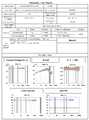
도 9a 내지 도 9d는 열충격 테스트 결과도이고, 도 10a 내지 도 10d는 상온온도 테스트 결과도이다. 도 9a는 백색 실리콘 에폭시 수지의 반사판(적층체(38))이 채용된 구조에 대해 대략 20mA의 정격전류(IF)을 -30℃ ~ 100℃ 의 온도범위에서 50회 정도 제공하여 본 열충격 테스트 리포트이고, 도 9b는 도 9a의 로오 데이터(raw data)이다. 도 9c는 백색 실리콘 에폭시 수지의 반사판(적층체(38))이 채용된 구조에 대해 대략 150mA의 정격전류(IF)을 -30℃ ~ 100℃ 의 온도범위에서 50사이클 정도 제공하여 본 열충격 테스트 리포트이고, 도 9d는 도 9c의 로오 데이터(raw data)이다. 도 10a는 백색 실리콘 에폭시 수지의 반사판(적층체(38))이 채 용된 구조의 엘이디 칩에 대략 20mA의 정격전류(IF)을 제공하되 25℃ 정도의 온도에서 장시간동안 점등시켰을 경우의 상온온도 테스트 리포트이다. 도 10b는 도 10a의 로오 데이터(raw data)이다. 도 10c는 백색 실리콘 에폭시 수지의 반사판(적층체(38))이 채용된 구조의 엘이디 칩에 대략 150mA의 정격전류(IF)을 제공하되 25℃ 정도의 온도에서 장시간동안 점등시켰을 경우의 상온온도 테스트 리포트이다. 도 10d는 도 10c의 로오 데이터(raw data)이다. 열충격 데이터를 보더라도 처음 1 사이클때와 50 사이클때의 정격전압(VF), 광도, XY색좌표, 색온도, 연색지수 등을 비교하여 보면 그리 차이가 없음을 알 수 있다. 상온온도 데이터를 보더라도 1시간때와 1500시간이 경과하였을 때의 정격전압(VF), 광도, XY색좌표, 색온도, 연색지수 등을 비교하여 보면 그리 차이가 없음을 알 수 있다.9A to 9D are thermal shock test results, and FIGS. 10A to 10D are room temperature test results. FIG. 9A shows the thermal shock test by providing a rated current IF of approximately 20 mA about 50 times in a temperature range of −30 ° C. to 100 ° C. for a structure employing a reflecting plate (laminate 38) of a white silicon epoxy resin. 9B is raw data of FIG. 9A. FIG. 9C shows the thermal shock test by providing about 150 cycles of a rated current IF of about 150 mA in a temperature range of -30 ° C. to 100 ° C. for a structure employing a reflecting plate (laminate 38) of a white silicon epoxy resin. 9d is raw data of FIG. 9c. 10A shows a room temperature when the LED chip having a structure of white silicon epoxy resin (laminate 38) is provided with a rated current (IF ) of approximately 20 mA, and is turned on for a long time at a temperature of about 25 ° C. This is a test report. FIG. 10B is the raw data of FIG. 10A. 10C shows a room temperature when the LED chip having the structure of the white silicon epoxy resin (laminate 38) is provided with a rated current IF of approximately 150 mA but is turned on for a long time at a temperature of about 25 ° C. This is a test report. FIG. 10D is the raw data of FIG. 10C. The thermal shock data shows that there is no difference when comparing the rated voltage (VF ), brightness, XY color coordinate, color temperature, and color rendering index at the first 1 cycle and 50 cycles. Even when looking at the room temperature temperature data, it can be seen that there is no difference when comparing the rated voltage (VF ), luminous intensity, XY color coordinate, color temperature, and color rendering index at 1 hour and 1500 hours.
다시 말해서, 본 발명의 구조는 일반 플라스틱 패키지 및 일반 세라믹 패키지에 비해 열충격 데이터가 우수함을 알 수 있다. 즉, 본 발명의 구조에 의하면 열로 인한 표면 열화 현상(황변 현상)이 적어 직접적으로 광 열화(light degradation)가 적을 뿐만 아니라 광특성 변화가 우수함을 알 수 있다.In other words, the structure of the present invention can be seen that the thermal shock data is superior to the general plastic package and the general ceramic package. That is, according to the structure of the present invention, the surface deterioration phenomenon due to heat (yellowing phenomenon) can be seen that not only the light degradation directly (light degradation), but also excellent optical properties change.
도 11은 PCT(Pressure Cooker Test)후 제품의 패키지 내습여부를 확인한 도면이다. 온도 100℃, 기압 2atm, 습도 120%RH에서 60시간 동안 PCT(Pressure Cooker Test)를 실시한 후에 제품의 패키지 내습여부를 확인하여 보았다. 내습여부를 확인하기 위해 사용된 잉크는 매표화학이라는 회사의 빨간색의 스탬프 잉 크(STAMP INK)이다.11 is a view confirming whether the package moisture resistance of the product after the PCT (Pressure Cooker Test). After a 60-hour PCT (Pressure Cooker Test) at a temperature of 100 ℃, atmospheric pressure 2atm,
실험 진행 사항은 하기의 표 3과 같다.Experimental progress is shown in Table 3 below.
(표 3)(Table 3)
1
One
10AZ-c
(기존 모델)WH3030
10AZ-c
(original model)
LTCC 기판
LTCC Board
+ Yellow PhosporOE-6630 A / B
+ Yellow Phospor
PCT 60시간
3개
Three
46시간
46 hours
2
2
10AZ-f
(기존 모델)WH5050
10AZ-f
(original model)
LTCC 기판
LTCC Board
+ Yellow PhosporOE-6630 A / B
+ Yellow Phospor
PCT 60시간
3개
Three
46시간
46 hours
3
3
10AZ-c{ER}
(본원 모델)WH3030
10AZ-c {ER}
(Original model)
LTCC 기판
LTCC Board
+ Yellow PhosporOE-6630 A / B
+ Yellow Phospor
PCT 60시간
10개
10 things
46시간
46 hours
상기와 같은 조건으로 PCT(Pressure Cooker Test)후에 제품의 패키지 내습여부를 확인하여 본 결과, 도 11에서와 같이 본원 모델에서는 빨간색의 잉크가 침투되지 않음을 확인하였다. 이는 일반 플라스틱 패키지 및 세라믹 패키지와 비교하여 실리콘과 기판 사이의 들뜸으로 인한 제품 영향을 테스트한 것으로, 이상없음을 확인할 수 있었다.As a result of checking whether the package moisture resistance of the product after PCT (Pressure Cooker Test) under the above conditions, it was confirmed that the red ink does not penetrate in the present model as shown in FIG. Compared with the general plastic package and the ceramic package, this test was conducted on the product influence caused by the lifting between the silicon and the substrate.
도 12는 엘이디 칩을 20mA 블루칩으로 한 경우의 특성을 비교한 도면이다. 도 12는 고정 패키지에 칩 메이커별로 백색 실리콘 에폭시 수지의 반사판(도 3, 도 4의 38)을 적용하기 전과 후를 비교한 결과도이다. 도 12에서는 정격전압(IF) 및 색온도(CCT)를 동일하게(또는 거의 유사하게) 맞춰놓고 ER전(즉, 백색 실리콘 에폭시 수지의 반사판을 적용하기 전)과 ER후(즉, 백색 실리콘 에폭시 수지의 반사판을 적용한 후)의 광도(CD)의 변화를 보면 ER후의 광도가 ER전의 광도에 비해 향상되었음 을 알 수 있다.12 is a diagram comparing the characteristics when the LED chip is a 20mA blue chip. 12 is a result of comparing the before and after applying the reflecting plate (38 of Fig. 3, 4) of the white silicon epoxy resin for each chip maker to the fixed package. In Fig. 12, the rated voltage IF and the color temperature CCT are set equally (or almost similarly), before ER (i.e. before applying a reflector of white silicone epoxy resin) and after ER (i.e. white silicon epoxy). The change in luminous intensity (CD) of the resin after applying the reflector plate shows that the luminous intensity after ER is improved compared to the luminous intensity before ER.
도 13은 엘이디 칩을 350mA 이상의 파워 칩으로 한 경우의 광효율을 비교한 도면이다. 도 13은 고정 패키지에 칩 메이커별로 하이파워 칩을 채용하고서 백색 실리콘 에폭시 수지의 반사판(도 3, 도 4의 38)을 적용하기 전과 후를 비교한 결과도이다. 도 13에서는 ER전(즉, 백색 실리콘 에폭시 수지의 반사판을 적용하기 전)과 ER후(즉, 백색 실리콘 에폭시 수지의 반사판을 적용한 후)의 광도(CD), 지향각, 총광량(TLF)의 변화를 보면 ER후의 패키지의 광도, 지향각, 총광량이 ER전에 비해 향상되었음을 확연히 알 수 있다. 특히, 백색 실리콘 에폭시 수지의 반사판(도 3, 도 4의 38)을 적용한 경우에는 지향각이 커짐에도 불구하고 총광량이 커짐을 알 수 있다.Fig. 13 is a view comparing light efficiency when the LED chip is a power chip of 350 mA or more. 13 is a result of comparing the before and after applying a high-power chip for each chip maker in the fixed package to apply the reflecting plate (38 in Figs. 3, 4) of the white silicon epoxy resin. In Fig. 13, before the ER (i.e. before applying the reflecting plate of the white silicone epoxy resin) and after the ER (i.e. after applying the reflecting plate of the white silicone epoxy resin), the intensity (CD), the direction angle, and the total amount of light (TLF) The change clearly shows that the luminosity, beam angle, and total light intensity of the package after ER are improved compared to before ER. In particular, when the reflecting plate (38 of Fig. 3, 4) of the white silicone epoxy resin is applied, it can be seen that the total amount of light increases even though the directivity angle is increased.
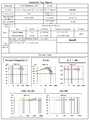
도 14는 세라믹 패키지별 광효율을 비교한 도면이다. 서로 다른 각종의 패키지에 칩 메이커별로 기존 구조와 백색 실리콘 에폭시 수지의 반사판(ER)을 적용한 구조를 비교하여 본 결과, 광도, 지향각, 색온도(CCT) 등에서 확연하게 향상되었음을 알 수 있다. 예를 들어, "2812"의 패키지 사이즈를 갖는 기존의 경우는 화이트 에폭시를 접착제로 사용하여 엘이디 칩(34)을 직접 기판(30)에 접촉하고 캐비티내에 옐로우 형광체를 충전시킨 것이다. "2812"의 패키지 사이즈를 갖는 본 발명의 경우(본원)는 화이트 에폭시를 접착제로 사용하여 엘이디 칩(34)을 직접 기판(30)에 접촉하고 충전체(38)를 형성하고 충전체(38)의 상부 공간에 옐로우 형광체를 충 전시킨 것이다. 도 14에서, 다른 경우도 이와 유사하게 해석하면 된다. 예를 들어, Ag 에폭시는 접착제로 사용되고, 투명 실리콘(clear silicon)은 캐비티내에 충전되는 것이다. 도 13에서, 기존 구조의 경우에는 모두 통상적인 금속의 반사판을 갖는 것으로 이해하면 된다. 예를 들어, 도 14에서 5050패키지에 대한 본 발명의 에폭시 계열의 반사판을 처리하기 전(기존)과 후(본원)을 비교하여 보면, 색온도를 5116K 및 5012K로 거의 동일하게 맞추고 정격전류 및 지향각을 각각 동일하게 맞춘 후에 실험해 본 결과 백색 실리콘 에폭시 수지의 반사판(도 3, 도 4의 38)을 채용한 구조가 기존 구조에 비해 효율(예컨대, 광도)이 향상되었음을 알 수 있다. 색온도는 동일하게 맞추는 것이 제일 정확한 데이터가 되겠으나, 동일하게 맞추기가 어려워서 비슷하게 맞추고서 실험한 데이터이다.14 is a view comparing light efficiency for each ceramic package. As a result of comparing the conventional structure and the structure in which the reflector plate (ER) of the white silicon epoxy resin is applied to various packages, it can be seen that the brightness, the directivity, and the color temperature (CCT) are significantly improved. For example, in the conventional case having a package size of "2812", the white chip is used as an adhesive to directly contact the
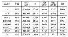
도 15는 세라믹 소재의 패키지와 플라스틱 패키지에서의 광효율 향상을 시험한 도면이다. 도 15에서 세라믹 소재의 패키지는 LTCC기판을 사용한 패키지를 의미하고, 플라스틱 패키지는 리드 프레임 기판을 사용한 패키지를 의미한다. 플라스틱 패키지에 칩 메이커별로 기존 구조와 백색 실리콘 에폭시 수지의 반사판(ER)을 적용한 구조를 비교하여 본 결과, 광도, 총광량에서 확연하게 향상되었음을 알 수 있다. 도 15에서 패키지(PKG)의 단위는 mm이고 도시된 사이즈는 패키지의 기판의 사이즈이다. 칩은 TG사의 경우 14mil, 24mil을 사용하였고, Cree사의 경우 40mil을 사용하였다. 기존 몰드 방식과 본 발명의 몰드 방식(백색 실리콘 에폭시 수지를 사용)을 비교하여 보면 광도 및 총광량에서 개선되었음을 알 수 있다.FIG. 15 is a view illustrating a test of improving light efficiency in a package of a ceramic material and a plastic package. FIG. In FIG. 15, a package of ceramic material means a package using an LTCC substrate, and a plastic package means a package using a lead frame substrate. As a result of comparing the structure of the plastic package with the conventional structure and the reflecting plate (ER) of the white silicon epoxy resin for each chip maker, it can be seen that the brightness and the total light quantity are significantly improved. The unit of the package PKG in FIG. 15 is mm and the size shown is the size of the substrate of the package. The chip used 14 mil and 24 mil for TG and 40 mil for Cree. Comparing the conventional mold method and the mold method of the present invention (using a white silicone epoxy resin) it can be seen that the improvement in the brightness and the total light amount.
도 16은 본 발명의 실시예에 따른 전자부품 패키지의 효과를 설명하기 위한 실험 결과표이다. 도 16은 전자부품 패키지가 백색광을 구현하는 경우의 두 가지의 패키지 사이즈별로 기존 구조와 본원 구조의 차이에 의한 효과를 설명하는 도면이다. 도 16에서 알 수 있듯이, 3030(1.0t) 패키지 사이즈의 경우 기존 구조에 비해 본원 구조와 같은 백색 실리콘 에폭시 수지의 반사판을 적용하게 되면 광도(Luminous Intensity) 및 총광량(Total luminance flux)에서 상당히 상승하였음을 알 수 있다. 5050(1.0t) 패키지 사이즈의 경우 기존 구조에 비해 본원 구조가 광도(Luminous Intensity) 및 총광량(Total luminance flux)에서 상당히 상승하였음을 알 수 있다16 is an experimental result table for explaining the effect of the electronic component package according to an embodiment of the present invention. FIG. 16 is a diagram illustrating an effect due to a difference between an existing structure and the present structure according to two package sizes when an electronic component package implements white light. As can be seen in FIG. 16, in the case of the 3030 (1.0t) package size, when the reflecting plate of the white silicon epoxy resin like the present structure is applied, the increase in luminous intensity and total luminance flux is significantly increased. It can be seen that. In the case of the 5050 (1.0t) package size, it can be seen that the structure of the present invention is significantly increased in the luminous intensity and the total luminance flux compared to the existing structure.
도 17은 본 발명의 실시예에 따른 전자부품 패키지의 효과를 설명하기 위한 실험 결과표이다. 도 17은 전자부품 패키지가 백색광을 구현하는 경우의 다양한 패키지 사이즈별로 기존 구조와 본원 구조의 차이에 의한 효과를 설명하는 도면이다. 도 17에서 알 수 있듯이, 패키지 사이즈를 다양하게 가변시켜 광도 및 총광량을 실험해본 결과, 본원 구조가 광도 및 총광량에서 향상되었음을 알 수 있다. 특히, 기존의 7090(4.2t)와 7090(1.2t)의 총광량(TLF)과 본 발명의 백색 실리콘 에폭시 수지의 반사판을 적용한 7090(4.2t)와 7090(1.3t)의 총광량(TLF)을 비교하여 보면, 본 발명의 백색 실리콘 에폭시 수지의 반사판을 적용한 7090(4.2t)와 7090(1.3t)의 총광량(TLF)이 상당히 상승하였음을 알 수 있다.17 is an experimental result table for explaining the effect of the electronic component package according to an embodiment of the present invention. FIG. 17 is a diagram illustrating an effect due to a difference between an existing structure and the present structure according to various package sizes when an electronic component package implements white light. As can be seen in Figure 17, by varying the package size to test the light intensity and total light, it can be seen that the structure of the present application is improved in the light intensity and total light amount. In particular, the total light amount (TLF) of the existing 7090 (4.2t) and 7090 (1.2t) and the total light amount (TLF) of 7090 (4.2t) and 7090 (1.3t) to which the reflecting plate of the white silicone epoxy resin of the present invention is applied. In comparison, it can be seen that the total light amount (TLF) of 7090 (4.2t) and 7090 (1.3t) to which the reflecting plate of the white silicone epoxy resin of the present invention is applied is significantly increased.
도 18은 본 발명의 실시예에 따른 전자부품 패키지의 효과를 설명하기 위한 실험 결과표이다. 도 18의 상부의 내용은 5050(3.2t)의 전자부품 패키지의 발광원을 녹색 및 적색으로 각각 구현하는 경우의 기존 구조와 본원 구조의 차이에 의한 효과를 설명하기 위한 데이터이다. 도 18의 하부의 내용은 4508(1.3t)의 전자부품 패키지가 백색광을 구현하는 경우의 기존 구조와 본원 구조의 차이에 의한 효과를 설명하기 위한 데이터이다. 각각의 경우를 보면, 본원 구조가 광도에서 향상되었음을 알 수 있다.18 is an experimental result table for explaining the effect of the electronic component package according to an embodiment of the present invention. The upper portion of FIG. 18 is data for explaining the effects of differences between the existing structure and the present structure when the light emitting sources of the 5050 (3.2t) electronic component package are implemented in green and red, respectively. The lower part of FIG. 18 is data for explaining the effects of the difference between the existing structure and the present structure when the 4508 (1.3t) electronic component package implements white light. In each case, it can be seen that the structure of the present application is improved in light intensity.
한편, 본 발명은 상술한 실시예로만 한정되는 것이 아니라 본 발명의 요지를 벗어나지 않는 범위내에서 수정 및 변형하여 실시할 수 있고, 그러한 수정 및 변형이 가해진 기술사상 역시 이하의 특허청구범위에 속하는 것으로 보아야 한다.On the other hand, the present invention is not limited only to the above-described embodiments and can be carried out by modifications and variations within the scope not departing from the gist of the present invention, the technical idea that such modifications and variations are also within the scope of the claims Must see
도 1은 종래의 LED패키지 구조의 개략도이다.1 is a schematic diagram of a structure of a conventional LED package.
도 2는 종래의 금속 반사판을 갖춘 LED 패키지의 사시도이다.2 is a perspective view of an LED package with a conventional metal reflector.
도 3은 본 발명의 실시예에 따른 전자부품 패키지의 단면도이다.3 is a cross-sectional view of an electronic component package according to an embodiment of the present invention.
도 4는 도 3의 변형예이다.4 is a modification of FIG. 3.
도 5는 본 발명의 실시예에 따른 전자부품 패키지의 제조방법을 설명하는 플로우차트이다.5 is a flowchart illustrating a method of manufacturing an electronic component package according to an embodiment of the present invention.
도 6 및 도 7은 도 5의 플로우차트 설명에 채용되는 사진이다.6 and 7 are photographs employed in the flowchart description of FIG. 5.
도 8a는 TiO2를 충전체의 재료로 사용한 경우의 흡수도 그래프이고, 도 8b는 ZnO를 충전체의 재료로 사용한 경우의 흡수도 그래프이다.8A is a graph of absorbance when TiO2 is used as the material of the filler, and FIG. 8B is a graph of absorbance when ZnO is used as the material of the filler.
도 9a 내지 도 9d은 열충격 테스트 결과도이다.9a to 9d are thermal shock test results.
도 10a 내지 도 10d는 상온온도 테스트 결과도이다.10A to 10D are diagrams of room temperature test results.
도 11은 PCT(Pressure Cooker Test)후 제품의 패키지 내습여부를 확인한 도면이다.11 is a view confirming whether the package moisture resistance of the product after the PCT (Pressure Cooker Test).
도 12는 20mA 블루칩의 특성을 비교한 도면이다.12 is a view comparing the characteristics of the 20mA blue chip.
도 13은 350mA 이상의 파워 칩의 광효율을 비교한 도면이다.13 is a view comparing light efficiency of power chips of 350 mA or more.
도 14는 세라믹 패키지별 광효율을 비교한 도면이다.14 is a view comparing light efficiency for each ceramic package.
도 15는 세라믹 소재의 패키지와 플라스틱 패키지에서의 광효율 향상을 시험한 도면이다.FIG. 15 is a view illustrating an improvement in light efficiency in a package of a ceramic material and a plastic package. FIG.
도 16 내지 도 18은 패키지 사이즈, 파워, 컬러별로 구체적인 실험을 통해 광효율을 검증한 실험 결과표이다.16 to 18 is a table of results of verifying the light efficiency through a specific experiment for each package size, power, color.
< 도면의 주요부분에 대한 부호의 설명 >Description of the Related Art
30 : 기판32 : 다이30
34 : 엘이디 칩36 : 와이어34: LED chip 36: wire
38 : 충전체38: charging body
Claims (16)
Translated fromKoreanPriority Applications (1)
| Application Number | Priority Date | Filing Date | Title |
|---|---|---|---|
| PCT/KR2008/007332WO2009075530A2 (en) | 2007-12-13 | 2008-12-11 | Semiconductor and manufacturing method thereof |
Applications Claiming Priority (4)
| Application Number | Priority Date | Filing Date | Title |
|---|---|---|---|
| KR1020070129775 | 2007-12-13 | ||
| KR20070129775 | 2007-12-13 | ||
| KR20080031620 | 2008-04-04 | ||
| KR1020080031620 | 2008-04-04 |
Publications (2)
| Publication Number | Publication Date |
|---|---|
| KR20090063054A KR20090063054A (en) | 2009-06-17 |
| KR100974604B1true KR100974604B1 (en) | 2010-08-06 |
Family
ID=40992217
Family Applications (1)
| Application Number | Title | Priority Date | Filing Date |
|---|---|---|---|
| KR1020080035172AActiveKR100974604B1 (en) | 2007-12-13 | 2008-04-16 | Electronic component package and manufacturing method thereof |
Country Status (1)
| Country | Link |
|---|---|
| KR (1) | KR100974604B1 (en) |
Cited By (1)
| Publication number | Priority date | Publication date | Assignee | Title |
|---|---|---|---|---|
| KR101483010B1 (en)* | 2013-07-29 | 2015-01-19 | 주식회사 굿엘이디 | Light Emitting Diode package |
Families Citing this family (7)
| Publication number | Priority date | Publication date | Assignee | Title |
|---|---|---|---|---|
| KR101108984B1 (en)* | 2009-12-03 | 2012-01-31 | (주) 아모엘이디 | Multichip LED Package and Manufacturing Method Thereof |
| KR101107144B1 (en)* | 2009-12-17 | 2012-01-31 | (주) 아모엘이디 | Manufacturing method of LED package |
| KR101115460B1 (en)* | 2010-04-02 | 2012-02-24 | (주) 아모엘이디 | LED package |
| US9634208B2 (en)* | 2014-01-29 | 2017-04-25 | Koninklijke Philips N.V. | Shallow reflector cup for phosphor-converted LED filled with encapsulant |
| KR102344533B1 (en) | 2015-02-12 | 2021-12-29 | 엘지이노텍 주식회사 | Lighting emitting device package |
| CN105428502A (en)* | 2015-12-15 | 2016-03-23 | 江苏稳润光电有限公司 | White light LED wafer packaging structure and packaging method |
| CN110416386B (en)* | 2019-08-02 | 2024-09-03 | 山西高科华兴电子科技有限公司 | Method for improving brightness of dark color plastic bowl cup packaged LED and LED |
Citations (2)
| Publication number | Priority date | Publication date | Assignee | Title |
|---|---|---|---|---|
| KR100445666B1 (en) | 2003-03-10 | 2004-08-23 | 루미마이크로 주식회사 | Light emitting device having light emitting surface of concave lens and method for manufacturing thereof |
| KR100616053B1 (en) | 2002-04-30 | 2006-08-28 | 도요다 고세이 가부시키가이샤 | Light emitting diode |
- 2008
- 2008-04-16KRKR1020080035172Apatent/KR100974604B1/enactiveActive
Patent Citations (2)
| Publication number | Priority date | Publication date | Assignee | Title |
|---|---|---|---|---|
| KR100616053B1 (en) | 2002-04-30 | 2006-08-28 | 도요다 고세이 가부시키가이샤 | Light emitting diode |
| KR100445666B1 (en) | 2003-03-10 | 2004-08-23 | 루미마이크로 주식회사 | Light emitting device having light emitting surface of concave lens and method for manufacturing thereof |
Cited By (1)
| Publication number | Priority date | Publication date | Assignee | Title |
|---|---|---|---|---|
| KR101483010B1 (en)* | 2013-07-29 | 2015-01-19 | 주식회사 굿엘이디 | Light Emitting Diode package |
Also Published As
| Publication number | Publication date |
|---|---|
| KR20090063054A (en) | 2009-06-17 |
Similar Documents
| Publication | Publication Date | Title |
|---|---|---|
| KR100974604B1 (en) | Electronic component package and manufacturing method thereof | |
| CN103270614B (en) | Light emitting devices and methods | |
| EP1953834B1 (en) | Light-emitting device | |
| US10134961B2 (en) | Submount based surface mount device (SMD) light emitter components and methods | |
| EP1953835B1 (en) | Light-emitting device | |
| TWI523273B (en) | Light-emitting diode package with contrast surface | |
| US20130207130A1 (en) | Light emitter devices having improved light output and related methods | |
| KR101766299B1 (en) | Light emitting device package and method of manufacturing the light emitting device package | |
| CN104396036A (en) | Light emitter packages, systems, and methods | |
| KR20140038553A (en) | Light emitter device packages, components, and mehtods for improved chemical resistance and related methods | |
| EP1743358A2 (en) | Light emitting diode component | |
| KR20110095301A (en) | Multichip Light Emitting Diode Module | |
| KR20150094402A (en) | Light source package and a display device including the same | |
| KR102300558B1 (en) | Light source module | |
| EP1900040B1 (en) | Light emitting diode and method of fabricating the same | |
| CN102637812B (en) | Light emitting device package and manufacturing method thereof | |
| KR20080055549A (en) | Manufacturing method of LED package | |
| KR20150095430A (en) | Light emitting diode package and light emitting device using the same | |
| KR100954453B1 (en) | LED package | |
| KR101090991B1 (en) | LED package and method of manufacturing the LED package | |
| KR100996918B1 (en) | Electronic component package | |
| KR20160028014A (en) | Method of manufacturing a semiconductor device package | |
| KR20150121364A (en) | Semiconductor optical device and method of manufacturing the same | |
| CN203707120U (en) | Solid state transmitter package unit and multi-pixel transmitting package unit | |
| KR100979174B1 (en) | Multichip Package and Manufacturing Method Thereof |
Legal Events
| Date | Code | Title | Description |
|---|---|---|---|
| A201 | Request for examination | ||
| PA0109 | Patent application | St.27 status event code:A-0-1-A10-A12-nap-PA0109 | |
| PA0201 | Request for examination | St.27 status event code:A-1-2-D10-D11-exm-PA0201 | |
| N231 | Notification of change of applicant | ||
| PN2301 | Change of applicant | St.27 status event code:A-3-3-R10-R13-asn-PN2301 St.27 status event code:A-3-3-R10-R11-asn-PN2301 | |
| P22-X000 | Classification modified | St.27 status event code:A-2-2-P10-P22-nap-X000 | |
| R17-X000 | Change to representative recorded | St.27 status event code:A-3-3-R10-R17-oth-X000 | |
| PG1501 | Laying open of application | St.27 status event code:A-1-1-Q10-Q12-nap-PG1501 | |
| D13-X000 | Search requested | St.27 status event code:A-1-2-D10-D13-srh-X000 | |
| D14-X000 | Search report completed | St.27 status event code:A-1-2-D10-D14-srh-X000 | |
| E902 | Notification of reason for refusal | ||
| PE0902 | Notice of grounds for rejection | St.27 status event code:A-1-2-D10-D21-exm-PE0902 | |
| T11-X000 | Administrative time limit extension requested | St.27 status event code:U-3-3-T10-T11-oth-X000 | |
| P11-X000 | Amendment of application requested | St.27 status event code:A-2-2-P10-P11-nap-X000 | |
| P13-X000 | Application amended | St.27 status event code:A-2-2-P10-P13-nap-X000 | |
| E701 | Decision to grant or registration of patent right | ||
| PE0701 | Decision of registration | St.27 status event code:A-1-2-D10-D22-exm-PE0701 | |
| GRNT | Written decision to grant | ||
| PR0701 | Registration of establishment | St.27 status event code:A-2-4-F10-F11-exm-PR0701 | |
| PR1002 | Payment of registration fee | St.27 status event code:A-2-2-U10-U11-oth-PR1002 Fee payment year number:1 | |
| PG1601 | Publication of registration | St.27 status event code:A-4-4-Q10-Q13-nap-PG1601 | |
| FPAY | Annual fee payment | Payment date:20130801 Year of fee payment:4 | |
| PR1001 | Payment of annual fee | St.27 status event code:A-4-4-U10-U11-oth-PR1001 Fee payment year number:4 | |
| PN2301 | Change of applicant | St.27 status event code:A-5-5-R10-R13-asn-PN2301 St.27 status event code:A-5-5-R10-R11-asn-PN2301 | |
| PN2301 | Change of applicant | St.27 status event code:A-5-5-R10-R11-asn-PN2301 | |
| PN2301 | Change of applicant | St.27 status event code:A-5-5-R10-R14-asn-PN2301 | |
| PR1001 | Payment of annual fee | St.27 status event code:A-4-4-U10-U11-oth-PR1001 Fee payment year number:5 | |
| FPAY | Annual fee payment | Payment date:20150803 Year of fee payment:6 | |
| PR1001 | Payment of annual fee | St.27 status event code:A-4-4-U10-U11-oth-PR1001 Fee payment year number:6 | |
| FPAY | Annual fee payment | Payment date:20160804 Year of fee payment:7 | |
| PR1001 | Payment of annual fee | St.27 status event code:A-4-4-U10-U11-oth-PR1001 Fee payment year number:7 | |
| P22-X000 | Classification modified | St.27 status event code:A-4-4-P10-P22-nap-X000 | |
| FPAY | Annual fee payment | Payment date:20170712 Year of fee payment:8 | |
| PR1001 | Payment of annual fee | St.27 status event code:A-4-4-U10-U11-oth-PR1001 Fee payment year number:8 | |
| PR1001 | Payment of annual fee | St.27 status event code:A-4-4-U10-U11-oth-PR1001 Fee payment year number:9 | |
| P22-X000 | Classification modified | St.27 status event code:A-4-4-P10-P22-nap-X000 | |
| FPAY | Annual fee payment | Payment date:20190711 Year of fee payment:10 | |
| PR1001 | Payment of annual fee | St.27 status event code:A-4-4-U10-U11-oth-PR1001 Fee payment year number:10 | |
| PR1001 | Payment of annual fee | St.27 status event code:A-4-4-U10-U11-oth-PR1001 Fee payment year number:11 | |
| PR1001 | Payment of annual fee | St.27 status event code:A-4-4-U10-U11-oth-PR1001 Fee payment year number:12 | |
| PR1001 | Payment of annual fee | St.27 status event code:A-4-4-U10-U11-oth-PR1001 Fee payment year number:13 | |
| PR1001 | Payment of annual fee | St.27 status event code:A-4-4-U10-U11-oth-PR1001 Fee payment year number:14 | |
| PR1001 | Payment of annual fee | St.27 status event code:A-4-4-U10-U11-oth-PR1001 Fee payment year number:15 | |
| P22-X000 | Classification modified | St.27 status event code:A-4-4-P10-P22-nap-X000 | |
| PR1001 | Payment of annual fee | St.27 status event code:A-4-4-U10-U11-oth-PR1001 Fee payment year number:16 |