KR100963027B1 - Thin film transistor, its manufacturing method, and flat panel display device comprising thin film transistor - Google Patents
Thin film transistor, its manufacturing method, and flat panel display device comprising thin film transistorDownload PDFInfo
- Publication number
- KR100963027B1 KR100963027B1KR1020080062418AKR20080062418AKR100963027B1KR 100963027 B1KR100963027 B1KR 100963027B1KR 1020080062418 AKR1020080062418 AKR 1020080062418AKR 20080062418 AKR20080062418 AKR 20080062418AKR 100963027 B1KR100963027 B1KR 100963027B1
- Authority
- KR
- South Korea
- Prior art keywords
- layer
- active layer
- thin film
- film transistor
- oxide semiconductor
- Prior art date
- Legal status (The legal status is an assumption and is not a legal conclusion. Google has not performed a legal analysis and makes no representation as to the accuracy of the status listed.)
- Active
Links
Images


Classifications
- H—ELECTRICITY
- H10—SEMICONDUCTOR DEVICES; ELECTRIC SOLID-STATE DEVICES NOT OTHERWISE PROVIDED FOR
- H10D—INORGANIC ELECTRIC SEMICONDUCTOR DEVICES
- H10D30/00—Field-effect transistors [FET]
- H10D30/60—Insulated-gate field-effect transistors [IGFET]
- H10D30/67—Thin-film transistors [TFT]
- H10D30/674—Thin-film transistors [TFT] characterised by the active materials
- H10D30/6755—Oxide semiconductors, e.g. zinc oxide, copper aluminium oxide or cadmium stannate
- G—PHYSICS
- G02—OPTICS
- G02F—OPTICAL DEVICES OR ARRANGEMENTS FOR THE CONTROL OF LIGHT BY MODIFICATION OF THE OPTICAL PROPERTIES OF THE MEDIA OF THE ELEMENTS INVOLVED THEREIN; NON-LINEAR OPTICS; FREQUENCY-CHANGING OF LIGHT; OPTICAL LOGIC ELEMENTS; OPTICAL ANALOGUE/DIGITAL CONVERTERS
- G02F1/00—Devices or arrangements for the control of the intensity, colour, phase, polarisation or direction of light arriving from an independent light source, e.g. switching, gating or modulating; Non-linear optics
- G02F1/01—Devices or arrangements for the control of the intensity, colour, phase, polarisation or direction of light arriving from an independent light source, e.g. switching, gating or modulating; Non-linear optics for the control of the intensity, phase, polarisation or colour
- G02F1/13—Devices or arrangements for the control of the intensity, colour, phase, polarisation or direction of light arriving from an independent light source, e.g. switching, gating or modulating; Non-linear optics for the control of the intensity, phase, polarisation or colour based on liquid crystals, e.g. single liquid crystal display cells
- G02F1/133—Constructional arrangements; Operation of liquid crystal cells; Circuit arrangements
- G02F1/136—Liquid crystal cells structurally associated with a semi-conducting layer or substrate, e.g. cells forming part of an integrated circuit
- G02F1/1362—Active matrix addressed cells
- G02F1/1368—Active matrix addressed cells in which the switching element is a three-electrode device
- H—ELECTRICITY
- H10—SEMICONDUCTOR DEVICES; ELECTRIC SOLID-STATE DEVICES NOT OTHERWISE PROVIDED FOR
- H10D—INORGANIC ELECTRIC SEMICONDUCTOR DEVICES
- H10D30/00—Field-effect transistors [FET]
- H10D30/01—Manufacture or treatment
- H10D30/021—Manufacture or treatment of FETs having insulated gates [IGFET]
- H10D30/031—Manufacture or treatment of FETs having insulated gates [IGFET] of thin-film transistors [TFT]
- H—ELECTRICITY
- H10—SEMICONDUCTOR DEVICES; ELECTRIC SOLID-STATE DEVICES NOT OTHERWISE PROVIDED FOR
- H10D—INORGANIC ELECTRIC SEMICONDUCTOR DEVICES
- H10D30/00—Field-effect transistors [FET]
- H10D30/60—Insulated-gate field-effect transistors [IGFET]
- H10D30/67—Thin-film transistors [TFT]
- H10D30/6704—Thin-film transistors [TFT] having supplementary regions or layers in the thin films or in the insulated bulk substrates for controlling properties of the device
- H—ELECTRICITY
- H10—SEMICONDUCTOR DEVICES; ELECTRIC SOLID-STATE DEVICES NOT OTHERWISE PROVIDED FOR
- H10D—INORGANIC ELECTRIC SEMICONDUCTOR DEVICES
- H10D30/00—Field-effect transistors [FET]
- H10D30/60—Insulated-gate field-effect transistors [IGFET]
- H10D30/67—Thin-film transistors [TFT]
- H10D30/6729—Thin-film transistors [TFT] characterised by the electrodes
- H10D30/6737—Thin-film transistors [TFT] characterised by the electrodes characterised by the electrode materials
- H10D30/6739—Conductor-insulator-semiconductor electrodes
- H—ELECTRICITY
- H10—SEMICONDUCTOR DEVICES; ELECTRIC SOLID-STATE DEVICES NOT OTHERWISE PROVIDED FOR
- H10D—INORGANIC ELECTRIC SEMICONDUCTOR DEVICES
- H10D30/00—Field-effect transistors [FET]
- H10D30/60—Insulated-gate field-effect transistors [IGFET]
- H10D30/67—Thin-film transistors [TFT]
- H10D30/6757—Thin-film transistors [TFT] characterised by the structure of the channel, e.g. transverse or longitudinal shape or doping profile
- H—ELECTRICITY
- H10—SEMICONDUCTOR DEVICES; ELECTRIC SOLID-STATE DEVICES NOT OTHERWISE PROVIDED FOR
- H10K—ORGANIC ELECTRIC SOLID-STATE DEVICES
- H10K59/00—Integrated devices, or assemblies of multiple devices, comprising at least one organic light-emitting element covered by group H10K50/00
- H10K59/10—OLED displays
- H10K59/12—Active-matrix OLED [AMOLED] displays
- H10K59/121—Active-matrix OLED [AMOLED] displays characterised by the geometry or disposition of pixel elements
- H10K59/1213—Active-matrix OLED [AMOLED] displays characterised by the geometry or disposition of pixel elements the pixel elements being TFTs
Landscapes
- Physics & Mathematics (AREA)
- Nonlinear Science (AREA)
- Engineering & Computer Science (AREA)
- Microelectronics & Electronic Packaging (AREA)
- Crystallography & Structural Chemistry (AREA)
- Chemical & Material Sciences (AREA)
- Mathematical Physics (AREA)
- Geometry (AREA)
- General Physics & Mathematics (AREA)
- Optics & Photonics (AREA)
- Thin Film Transistor (AREA)
- Liquid Crystal (AREA)
- Devices For Indicating Variable Information By Combining Individual Elements (AREA)
Abstract
Translated fromKoreanDescription
Translated fromKorean본 발명은 산화물 반도체를 활성층으로 하는 박막 트랜지스터, 그의 제조 방법 및 박막 트랜지스터를 구비하는 평판 표시 장치에 관한 것으로, 보다 상세하게는 활성층의 일면 또는 양면에 계면 안정화층(interfacial stability layer)이 구비된 박막 트랜지스터, 그의 제조 방법 및 박막 트랜지스터를 구비하는 평판 표시 장치에 관한 것이다.BACKGROUND OF THE
일반적으로 박막 트랜지스터(Thin Film Transistor)는 채널 영역, 소스 영역 및 드레인 영역을 제공하는 활성층(active layer)과, 채널 영역 상부에 형성되며 게이트 절연층에 의해 활성층과 전기적으로 절연되는 게이트 전극으로 이루어진다.In general, a thin film transistor includes an active layer providing a channel region, a source region, and a drain region, and a gate electrode formed on the channel region and electrically insulated from the active layer by a gate insulating layer.
이와 같이 이루어진 박막 트랜지스터의 활성층은 대개 비정질 실리콘(amorphous silicon)이나 폴리 실리콘(poly-silicon)과 같은 반도체 물질로 형성되는데, 활성층이 비정실 실리콘으로 형성되면 이동도(mobility)가 낮아 고속으로 동작되는 구동 회로의 구현이 어려우며, 폴리 실리콘으로 형성되면 이동도는 높지 만 문턱전압이 불균일하여 별도의 보상 회로가 부가되어야 하는 문제점이 있다.The active layer of the thin film transistor formed as described above is usually formed of a semiconductor material such as amorphous silicon or poly-silicon. When the active layer is formed of amorphous silicon, it is operated at high speed due to low mobility. It is difficult to implement the driving circuit, and when formed of polysilicon, the mobility is high, but there is a problem in that a separate compensation circuit should be added because the threshold voltage is uneven.
또한, 저온 폴리 실리콘(low temperature poly-silicon; LTPS)을 이용한 종래의 박막 트랜지스터 제조 방법은 레이저 열처리 등과 같은 고가의 공정이 포함되기 때문에 설비 투자 및 관리 비용이 높고 대면적의 기판에 적용이 어려운 문제점이 있다.In addition, the conventional thin film transistor manufacturing method using low temperature poly-silicon (LTPS) has a high cost of equipment investment and management cost and difficult to apply to a large-area substrate because expensive processes such as laser heat treatment are included. There is this.
이러한 문제점을 해결하기 위해 최근에는 산화물 반도체를 활성층으로 이용하는 연구가 진행되고 있다.In order to solve this problem, researches using an oxide semiconductor as an active layer have recently been conducted.
일본공개특허 2004-273614호에는 산화아연(zinc oxide; ZnO) 또는 산화아연(ZnO)을 주성분으로 하는 산화물 반도체를 활성층으로 이용한 박막 트랜지스터가 개시되어 있다.Japanese Laid-Open Patent Publication No. 2004-273614 discloses a thin film transistor using an oxide semiconductor containing zinc oxide (ZnO) or zinc oxide (ZnO) as an active layer.
산화아연(ZnO)을 주성분으로 하는 산화물 반도체는 비정질 형태이면서 이동도가 높기 때문에 안정적인 재료로서 평가되고 있다. 이러한 산화물 반도체를 활성층으로 이용하면 별도의 공정 장비를 추가적으로 구입하지 않고도 기존의 장비를 이용하여 박막 트랜지스터를 제조할 수 있다. 또한, 산화물 반도체는 저온에서 증착이 가능하고, 이온 주입이 필요하지 않으며, 또한, 스퍼터링(sputtering) 방법으로 증착할 수 있기 때문에 대면적 기판에도 적용이 가능하다.Oxide semiconductors containing zinc oxide (ZnO) as a main component have been evaluated as stable materials because they are amorphous and have high mobility. If the oxide semiconductor is used as an active layer, a thin film transistor can be manufactured using existing equipment without purchasing additional process equipment. In addition, since the oxide semiconductor can be deposited at a low temperature, does not require ion implantation, and can be deposited by a sputtering method, the oxide semiconductor can be applied to a large area substrate.
그러나 산화물 반도체를 활성층으로 하는 박막 트랜지스터는 구조 및 공정 조건에 따라 전기적 특성이 쉽게 변화되기 때문에 신뢰성이 낮은 문제점이 있다. 특히, 정전압 또는 정전류 구동시 문턱전압이 시간에 따라 양(+)의 방향으로 변화되는데, 이와 같은 현상의 주요 원인은 활성층과 게이트 절연층 또는 활성층과 보 호층의 계면 열화에 따른 전하 트랩핑(charge trapping)에 의한 것으로 추정된다.However, a thin film transistor having an oxide semiconductor as an active layer has a problem of low reliability because electrical characteristics are easily changed according to structure and process conditions. In particular, when driving a constant voltage or a constant current, the threshold voltage changes in a positive direction with time. The main cause of this phenomenon is charge trapping due to the interface degradation between the active layer and the gate insulating layer or the active layer and the protective layer. trapping).
본 발명의 목적은 활성층의 계면 특성이 향상될 수 있는 박막 트랜지스터, 그의 제조 방법 및 박막 트랜지스터를 구비하는 평판 표시 장치를 제공하는 데 있다.SUMMARY OF THE INVENTION An object of the present invention is to provide a thin film transistor, a method for manufacturing the same, and a flat panel display device including the thin film transistor, which can improve the interfacial properties of the active layer.
본 발명의 다른 목적은 활성층 계면에서의 전하 트랩핑을 방지할 수 있는 박막 트랜지스터, 그의 제조 방법 및 박막 트랜지스터를 구비하는 평판 표시 장치를 제공하는 데 있다.Another object of the present invention is to provide a thin film transistor capable of preventing charge trapping at the active layer interface, a manufacturing method thereof, and a flat panel display device having the thin film transistor.
본 발명의 또 다른 목적은 전기적 특성 및 신뢰성이 높은 박막 트랜지스터, 그의 제조 방법 및 박막 트랜지스터를 구비하는 평판 표시 장치를 제공하는 데 있다.Another object of the present invention is to provide a thin film transistor having high electrical characteristics and reliability, a method of manufacturing the same, and a flat panel display device having the thin film transistor.
상기한 목적을 달성하기 위한 본 발명의 일 측면에 따른 박막 트랜지스터는 기판; 상기 기판 상에 형성된 게이트 전극; 게이트 절연층에 의해 상기 게이트 전극과 절연되며 산화물 반도체로 이루어진 활성층; 상기 활성층과 연결되는 소스 전극 및 드레인 전극; 및 상기 활성층의 상부면 및 하부면 중 적어도 일 면에 형성된 계면 안정화층을 포함하며, 상기 계면 안정화층이 3.0 내지 8.0eV의 밴드갭을 갖는 산화물로 이루어진다.A thin film transistor according to an aspect of the present invention for achieving the above object is a substrate; A gate electrode formed on the substrate; An active layer made of an oxide semiconductor and insulated from the gate electrode by a gate insulating layer; A source electrode and a drain electrode connected to the active layer; And an interface stabilization layer formed on at least one of an upper surface and a lower surface of the active layer, wherein the interface stabilization layer is formed of an oxide having a band gap of 3.0 to 8.0 eV.
상기한 목적을 달성하기 위한 본 발명의 다른 일 측면에 따른 박막 트랜지스터의 제조 방법은 기판 상에 게이트 전극을 형성하는 단계; 상기 게이트 전극을 포 함하는 상부에 게이트 절연층을 형성하는 단계; 상기 게이트 절연층 상에 계면 안정화층 및 산화물 반도체층을 형성하는 단계; 상기 산화물 반도체층을 패터닝하여 활성층을 형성하는 단계; 및 상기 활성층과 연결되는 소스 전극 및 드레인 전극을 형성하는 단계를 포함하며, 상기 계면 안정화층을 3.0 내지 8.0eV의 밴드갭을 갖는 산화물로 형성한다.According to another aspect of the present invention, there is provided a method of manufacturing a thin film transistor, the method including: forming a gate electrode on a substrate; Forming a gate insulating layer on the top including the gate electrode; Forming an interface stabilization layer and an oxide semiconductor layer on the gate insulating layer; Patterning the oxide semiconductor layer to form an active layer; And forming a source electrode and a drain electrode connected to the active layer, wherein the interface stabilization layer is formed of an oxide having a band gap of 3.0 to 8.0 eV.
상기한 목적을 달성하기 위한 본 발명의 또 다른 일 측면에 따른 박막 트랜지스터의 제조 방법은 기판 상에 게이트 전극을 형성하는 단계; 상기 게이트 전극을 포함하는 상부에 게이트 절연층을 형성하는 단계; 상기 게이트 절연층 상에 산화물 반도체층 및 계면 안정화층을 형성하는 단계; 상기 계면 안정화층 및 산화물 반도체층을 패터닝하여 활성층을 형성하는 단계; 및 상기 활성층과 연결되는 소스 전극 및 드레인 전극을 형성하는 단계를 포함하며, 상기 계면 안정화층을 3.0 내지 8.0eV의 밴드갭을 갖는 산화물로 형성한다.According to still another aspect of the present invention, there is provided a method of manufacturing a thin film transistor, the method including forming a gate electrode on a substrate; Forming a gate insulating layer on the gate including the gate electrode; Forming an oxide semiconductor layer and an interface stabilization layer on the gate insulating layer; Patterning the interface stabilization layer and the oxide semiconductor layer to form an active layer; And forming a source electrode and a drain electrode connected to the active layer, wherein the interface stabilization layer is formed of an oxide having a band gap of 3.0 to 8.0 eV.
또한, 상기한 목적을 달성하기 위한 본 발명의 또 다른 일 측면에 따른 박막 트랜지스터를 구비하는 평판 표시 장치는 다수의 제 1 도전선과 제 2 도전선에 의해 다수의 화소가 정의되고, 각 화소로 공급되는 신호를 제어하는 박막 트랜지스터 및 박막 트랜지스터와 연결된 제 1 전극이 형성된 제 1 기판; 제 2 전극이 형성된 제 2 기판; 및 상기 제 1 전극과 제 2 전극 사이의 밀봉된 공간에 주입된 액정층을 포함하며, 상기 박막 트랜지스터는 상기 제 1 기판 상에 형성된 게이트 전극; 게이트 절연층에 의해 상기 게이트 전극과 절연되며 산화물 반도체로 이루어진 활성층; 상기 활성층과 연결되는 소스 전극 및 드레인 전극; 및 상기 활성층의 상부면 및 하부면 중 적어도 일 면에 형성된 계면 안정화층을 포함하며, 상기 계면 안정화층이 3.0 내지 8.0eV의 밴드갭을 갖는 산화물로 이루어진다.In addition, in the flat panel display device including the thin film transistor according to another aspect of the present invention for achieving the above object, a plurality of pixels are defined by a plurality of first conductive lines and second conductive lines, and supplied to each pixel. A first substrate having a thin film transistor for controlling a signal to be formed and a first electrode connected to the thin film transistor; A second substrate on which a second electrode is formed; And a liquid crystal layer injected into a sealed space between the first electrode and the second electrode, wherein the thin film transistor comprises: a gate electrode formed on the first substrate; An active layer made of an oxide semiconductor and insulated from the gate electrode by a gate insulating layer; A source electrode and a drain electrode connected to the active layer; And an interface stabilization layer formed on at least one of an upper surface and a lower surface of the active layer, wherein the interface stabilization layer is formed of an oxide having a band gap of 3.0 to 8.0 eV.
또한, 상기한 목적을 달성하기 위한 본 발명의 또 다른 일 측면에 따른 박막 트랜지스터를 구비하는 평판 표시 장치는 제 1 전극, 유기 박막층 및 제 2 전극으로 이루어진 유기전계발광 소자와, 상기 유기전계발광 소자의 동작을 제어하기 위한 박막 트랜지스터가 형성된 제 1 기판; 및 상기 제 1 기판에 대향되도록 배치된 제 2 기판을 포함하며, 상기 박막 트랜지스터는 상기 제 1 기판 상에 형성된 게이트 전극; 게이트 절연층에 의해 상기 게이트 전극과 절연되며 산화물 반도체로 이루어진 활성층; 상기 활성층과 연결되는 소스 전극 및 드레인 전극; 및 상기 활성층의 상부면 및 하부면 중 적어도 일 면에 형성된 계면 안정화층을 포함하며, 상기 계면 안정화층이 3.0 내지 8.0eV의 밴드갭을 갖는 산화물로 이루어진다.In addition, a flat panel display including a thin film transistor according to another aspect of the present invention for achieving the above object is an organic electroluminescent device consisting of a first electrode, an organic thin film layer and a second electrode, and the organic electroluminescent device A first substrate on which a thin film transistor for controlling operation of the substrate is formed; And a second substrate disposed to face the first substrate, wherein the thin film transistor comprises: a gate electrode formed on the first substrate; An active layer made of an oxide semiconductor and insulated from the gate electrode by a gate insulating layer; A source electrode and a drain electrode connected to the active layer; And an interface stabilization layer formed on at least one of an upper surface and a lower surface of the active layer, wherein the interface stabilization layer is formed of an oxide having a band gap of 3.0 to 8.0 eV.
본 발명의 박막 트랜지스터는 활성층의 일면 또는 양면에 계면 안정화층이 구비된다. 산화물을 포함하는 계면 안정화층은 게이트 절연층 및 보호층과 동질성을 갖기 때문에 화학적으로 높은 계면 안정성을 유지하며, 활성층과 같거나 활성층보다 큰 밴드갭을 갖기 때문에 물리적으로 전하 트랩핑을 억제하는 동시에 활성층을 보호한다. 따라서 높은 계면 안정성과 전하 이동도에 의해 문턱전압의 변화와 같은 전기적 특성 변화가 최소화되고, 온도 및 시간에 따른 신뢰성 저하가 방지될 수 있다. 본 발명의 박막 트랜지스터를 평판 표시 장치에 적용할 경우 안정된 전기적 특성에 의해 보다 향상된 화질을 구현할 수 있다.In the thin film transistor of the present invention, an interface stabilization layer is provided on one or both surfaces of the active layer. The interfacial stabilization layer including oxide maintains chemically high interfacial stability because of its homogeneity with the gate insulating layer and the protective layer, and physically suppresses charge trapping while simultaneously having a band gap equal to or larger than the active layer. To protect. Therefore, the change of electrical characteristics such as the change of the threshold voltage is minimized by the high interfacial stability and the charge mobility, and the degradation of reliability with temperature and time can be prevented. When the thin film transistor of the present invention is applied to a flat panel display, improved image quality can be realized by stable electrical characteristics.
이하, 첨부된 도면을 참조하여 본 발명의 바람직한 실시예를 상세히 설명하기로 한다. 이하의 실시예는 이 기술 분야에서 통상적인 지식을 가진 자에게 본 발명이 충분히 이해되도록 제공되는 것으로서, 여러 가지 형태로 변형될 수 있으며, 본 발명의 범위가 다음에 기술되는 실시예에 한정되는 것은 아니다.Hereinafter, exemplary embodiments of the present invention will be described in detail with reference to the accompanying drawings. The following embodiments are provided to those skilled in the art to fully understand the present invention, and may be modified in various forms, and the scope of the present invention is limited to the embodiments described below. no.
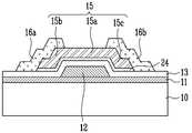
도 1은 본 발명의 제 1 실시예에 따른 박막 트랜지스터를 설명하기 위한 단면도로서, 하부 게이트(bottom gate) 구조의 일 예를 도시한다.1 is a cross-sectional view illustrating a thin film transistor according to a first exemplary embodiment of the present invention and illustrates an example of a bottom gate structure.
기판(10) 상에 버퍼층(11)이 형성되고, 버퍼층(11) 상에 게이트 전극(12)이 형성된다. 게이트 전극(12)을 포함하는 상부에는 게이트 절연층(13) 및 계면 안정화층(14)이 순차적으로 형성되고, 게이트 전극(12)을 포함하는 계면 안정화층(14) 상에는 산화물 반도체로 이루어진 활성층(15)이 형성된다. 활성층(15)의 양측에는 소스 및 드레인 전극(16a 및 16b)이 연결된다.The
계면 안정화층(14)은 활성층(15)과 같거나 활성층(15)보다 큰 밴드갭 예를 들어, 3.0 내지 8.0eV의 밴드갭을 갖는 산화물로서, SiOx, SiN, SiOxNy, SiOxCy, SiOxCyHz, SiOxFy, GeOx, GdOx, AlOx, GaOx, SbO, ZrOx, HfOx, TaOx, YOx, VOx, MgOx, CaOx, BaOx, SrOx 및 SOG(spin on glass)로 이루어진 군에서 선택될 수 있다.The
활성층(15)은 채널 영역(15a), 소스 영역(15b) 및 드레인 영역(15c)을 제공하며, 채널 영역(15a)이 게이트 전극(12)과 중첩되도록 배치된다. 활성층(15)을 구성하는 산화물 반도체는 산화아연(ZnO)을 포함하며, 갈륨(Ga), 인듐(In), 스태 늄(Sn), 지르코늄(Zr), 하프늄(Hf), 카드뮴(Cd), 은(Ag), 구리(Cu), 게르마늄(Ge), 가돌리늄(Gd) 및 바나듐(V) 중 적어도 하나의 이온이 도핑될 수 있다. 활성층(15)은 예를 들어, ZnO, ZnGaO, ZnInO, ZnSnO, GaInZnO, CdO, InO, GaO, SnO, AgO, CuO, GeO, GdO, HfO 등으로 형성될 수 있다.The
도 2는 본 발명의 제 2 실시예에 따른 박막 트랜지스터를 설명하기 위한 단면도로서, 도 1에 도시된 구조와의 차이점에 대해서만 설명하기로 한다.FIG. 2 is a cross-sectional view illustrating a thin film transistor according to a second exemplary embodiment of the present invention, and only differences from the structure shown in FIG. 1 will be described.
도 1의 박막 트랜지스터는 계면 안정화층(14)이 활성층(15)보다 넓게 형성된 구조인 반면, 도 2의 박막 트랜지스터는 계면 안정화층(24)과 활성층(15)이 동일한 크기로 형성된다. 계면 안정화층(24)과 활성층(15)의 측벽이 서로 일치되도록 계면 안정화층(24)과 활성층(15)을 동시에 패터닝할 수 있기 때문에 공정 단계를 감소시킬 수 있다.The thin film transistor of FIG. 1 has a structure in which the
도 3은 본 발명의 제 3 실시예에 따른 박막 트랜지스터를 설명하기 위한 단면도로서, 도 1 및 도 2에 도시된 구조와의 차이점에 대해서만 설명하기로 한다.3 is a cross-sectional view illustrating a thin film transistor according to a third exemplary embodiment of the present invention, and only differences from the structures shown in FIGS. 1 and 2 will be described.
도 1 및 도 2의 박막 트랜지스터는 소스 및 드레인 전극(16a 및 16b)이 활성층(15)과 직접 접촉되는 구조인 반면, 도 3의 박막 트랜지스터는 활성층(15)을 포함하는 상부에 보호층(26)이 형성되고, 보호층(26)에 형성된 콘택홀을 통해 소스 및 드레인 전극(27a 및 27b)이 활성층(15)과 연결된다. 보호층(26)은 아연(Zn), 갈륨(Ga), 인듐(In), 스태늄(Sn), 지르코늄(Zr), 하프늄(Hf), 카드뮴(Cd), 은(Ag), 구리(Cu), 게르마늄(Ge), 가돌리늄(Gd), 바나듐(V), 실리콘(Si) 및 알루미늄(Al)으로 이루어진 군에서 선택된 물질을 포함하는 산화물로 형성될 수 있다.The thin film transistors of FIGS. 1 and 2 have a structure in which the source and
상기 산화물로 이루어진 보호층(26)은 소스 및 드레인 전극(27a 및 27b)을 형성하는 식각 과정에서 채널 영역(15a)의 활성층(15)을 보호하는 동시에 식각 정지층(etch stop layer)으로 이용될 수 있기 때문에 플라즈마(plasma)나 산 용액(acid chemical)에 의한 활성층(15)의 피해(demage)를 방지한다.The
산화물 반도체는 플라즈마에 의해 쉽게 피해를 입거나 산 용액 등에 쉽게 식각된다. 그러므로 보호층이 없는 구조에서는 활성층 상부에 박막을 형성하거나, 형성된 박막을 식각할 때 플라즈마에 의한 피해가 발생되고, 피폭 효과(bombardment effect), 방사 효과(radiation effect) 등에 의해 케리어(carrier)가 증가하는 등의 전기적 특성 변화가 발생된다. 이러한 활성층의 전기적 특성 변화에 의해 박막 트랜지스터의 전기적 특성이 저하되고, 기판 내에서의 특성 산포도가 저하될 수 있다.Oxide semiconductors are easily damaged by plasma or are easily etched in acid solutions. Therefore, in the structure without a protective layer, when a thin film is formed on the active layer or when the thin film is etched, damages caused by plasma are generated, and carriers are increased due to bombardment effect and radiation effect. Electrical property changes such as Due to the change in electrical characteristics of the active layer, the electrical characteristics of the thin film transistor may be lowered, and the characteristic scattering degree in the substrate may be lowered.
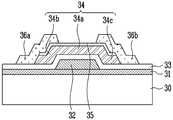
도 4는 본 발명의 제 4 실시예에 따른 박막 트랜지스터를 설명하기 위한 단면도로서, 도 1 내지 도 3의 박막 트랜지스터는 계면 안정화층(14 및 24)이 활성층(15)의 하부면에 형성된 구조인 반면, 도 4의 박막 트랜지스터는 계면 안정화층(35)이 활성층(34)의 상부면에 형성된다.4 is a cross-sectional view illustrating a thin film transistor according to a fourth exemplary embodiment of the present invention, wherein the thin film transistor of FIGS. On the other hand, in the thin film transistor of FIG. 4, the
도 4를 참조하면, 기판(30) 상에 버퍼층(31)이 형성되고, 버퍼층(31) 상에 게이트 전극(32)이 형성된다. 게이트 전극(32)을 포함하는 상부에는 게이트 절연층(33)이 형성되고, 게이트 전극(32)을 포함하는 게이트 절연층(33) 상에는 산화물 반도체로 이루어진 활성층(34)이 형성된다. 활성층(34) 상에는 계면 안정화층(35)이 형성되고, 계면 안정화층(35) 및 활성층(34)에는 소스 및 드레인 전극(36a 및 36b)이 연결된다.Referring to FIG. 4, a
활성층(24)은 채널 영역(34a), 소스 영역(34b) 및 드레인 영역(34c)을 제공하며, 채널 영역(34a)이 게이트 전극(32)과 중첩되도록 배치된다. 활성층(34)을 구성하는 산화물 반도체는 산화아연(ZnO)을 포함하며, 갈륨(Ga), 인듐(In), 스태늄(Sn), 지르코늄(Zr), 하프늄(Hf), 카드뮴(Cd), 은(Ag), 구리(Cu), 게르마늄(Ge), 가돌리늄(Gd) 및 바나듐(V) 중 적어도 하나의 이온이 도핑될 수 있다.The
계면 안정화층(35)은 활성층(34)과 같거나 활성층(34)보다 큰 밴드갭 예를 들어, 3.0 내지 8.0eV의 밴드갭을 갖는 산화물로서, SiOx, SiN, SiOxNy, SiOxCy, SiOxCyHz, SiOxFy, GeOx, GdOx, AlOx, GaOx, SbO, ZrOx, HfOx, TaOx, YOx, VOx, MgOx, CaOx, BaOx, SrOx 및 SOG로 이루어진 군에서 선택될 수 있다. 소스 및 드레인 전극(36a 및 36b)과 활성층(34) 사이에 개재되는 계면 안정화층(35)은 소스 및 드레인 전극(36a 및 36b)과 활성층(34)의 접촉저항이 낮게 유지될 수 있도록 예를 들어, 10 내지 20Å의 두께로 형성되는 것이 바람직하다.The
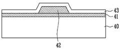
도 5는 본 발명의 제 5 실시예에 따른 박막 트랜지스터를 설명하기 위한 단면도로서, 도 1 내지 도 3의 박막 트랜지스터는 계면 안정화층(14 및 24)이 활성층(15)의 하부면에 형성되고, 도 4의 박막 트랜지스터는 계면 안정화층(35)이 활성층(34)의 상부면에 형성된 구조인 반면, 도 5의 박막 트랜지스터는 계면 안정화층(44 및 46)이 활성층(45)의 하부면과 상부면에 각각 형성된다.5 is a cross-sectional view illustrating a thin film transistor according to a fifth exemplary embodiment of the present invention. In the thin film transistors of FIGS. 1 to 3, interfacial stabilization layers 14 and 24 are formed on the lower surface of the
도 5를 참조하면, 기판(40) 상에 버퍼층(41)이 형성되고, 버퍼층(41) 상에 게이트 전극(42)이 형성된다. 게이트 전극(42)을 포함하는 상부에는 게이트 절연 층(43)이 형성되고, 게이트 전극(42)을 포함하는 게이트 절연층(43) 상에는 산화물 반도체로 이루어진 활성층(45)이 형성된다. 이 때 활성층(34)의 하부면과 상부면에는 계면 안정화층(44 및 46)이 각각 형성되고, 계면 안정화층(44 및 46) 및 활성층(45)에는 소스 및 드레인 전극(47a 및 47b)이 연결된다.Referring to FIG. 5, a
활성층(45)은 채널 영역(45a), 소스 영역(45b) 및 드레인 영역(45c)을 제공하며, 채널 영역(45a)이 게이트 전극(42)과 중첩되도록 배치된다. 활성층(45)을 구성하는 산화물 반도체는 산화아연(ZnO)을 포함하며, 갈륨(Ga), 인듐(In), 스태늄(Sn), 지르코늄(Zr), 하프늄(Hf), 카드뮴(Cd), 은(Ag), 구리(Cu), 게르마늄(Ge), 가돌리늄(Gd) 및 바나듐(V) 중 적어도 하나의 이온이 도핑될 수 있다.The
계면 안정화층(44 및 46)은 활성층(45)과 같거나 활성층(45)보다 큰 밴드갭 예를 들어, 3.0 내지 8.0eV의 밴드갭을 갖는 산화물로서, SiOx, SiN, SiOxNy, SiOxCy, SiOxCyHz, SiOxFy, GeOx, GdOx, AlOx, GaOx, SbO, ZrOx, HfOx, TaOx, YOx, VOx, MgOx, CaOx, BaOx, SrOx 및 SOG로 이루어진 군에서 선택될 수 있다. 활성층(45) 하부면의 계면 안정화층(44)은 활성층(45)을 충분히 보호하고 계면 안정성을 유지할 수 있도록 예를 들어, 50 내지 5000Å의 두께로 형성되는 것이 바람직하고, 활성층(45) 상부면의 계면 안정화층(46)은 소스 및 드레인 전극(47a 및 47b)과 활성층(45)의 접촉저항이 낮게 유지되도록 100Å 이하의 두께, 바람직하게는 10 내지 20Å의 두께로 형성되는 것이 바람직하다.The interfacial stabilization layers 44 and 46 are oxides having a bandgap equal to or larger than the
도 4 및 도 5의 박막 트랜지스터에서 계면 안정화층(35 및 46)은 소스 및 드레인 전극(36a 및 36b, 47a 및 47b)을 형성하는 식각 과정에서 채널 영역(34a 및 45a)의 활성층(34 및 45)을 보호하는 동시에 식각 정지층으로 이용되기 때문에 플라즈마 등에 의한 활성층(34 및 45)의 피해를 방지한다.In the thin film transistors of FIGS. 4 and 5, the interfacial stabilization layers 35 and 46 are
그러면 상기와 같이 구성된 본 발명에 따른 박막 트랜지스터의 제조 방법을 도 6a 내지 도 6d를 통해 상세히 설명하면 다음과 같다. 설명의 편의를 위해 도 5의 구조를 예로 들어 설명한다.Next, the manufacturing method of the thin film transistor according to the present invention configured as described above will be described in detail with reference to FIGS. 6A to 6D. For convenience of description, the structure of FIG. 5 will be described as an example.
도 6a를 참조하면, 기판(40) 상에 게이트 전극(42)을 형성한 후 게이트 전극(42)을 포함하는 상부에 게이트 절연층(43)을 형성한다. 이 때 불순물 확산 등을 방지하기 위해 기판(40) 상에 버퍼층(41)을 형성하고, 버퍼층(41) 상에 게이트 전극(42)을 형성할 수 있다. 기판(40)으로는 실리콘(Si) 등의 반도체 기판, 유리나 플라스틱 등의 절연 기판 또는 금속 기판을 사용할 수 있으며, 게이트 전극(42)은 Al, Cr, MoW 등의 금속으로 형성하고, 게이트 절연층(43)은 SiO2, SiNx, GaO3 등의 절연물로 형성한다.Referring to FIG. 6A, after the
도 6b를 참조하면, 게이트 절연층(43) 상에 계면 안정화층(44), 산화물 반도체층(45) 및 계면 안정화층(46)을 순차적으로 형성한다. 계면 안정화층(44 및 46)은 활성층(45)과 같거나 활성층(45)보다 큰 밴드갭 예를 들어, 3.0 내지 8.0eV의 밴드갭을 갖는 산화물로서, SiOx, SiN, SiOxNy, SiOxCy, SiOxCyHz, SiOxFy, GeOx, GdOx, AlOx, GaOx, SbO, ZrOx, HfOx, TaOx, YOx, VOx, MgOx, CaOx, BaOx, SrOx 및 SOG로 이루어진 군에서 선택될 수 있다.Referring to FIG. 6B, the
실리콘 산화물(SiOx) 및 알루미늄 산화물(AlOx)은 고주파(RF) 또는 직류(DC) 스퍼터링(sputterung) 증착 방법 등의 물리적인 방법으로 증착할 수 있다. 고주파(RF) 스퍼터링 방법으로 알루미늄 산화물(AlOx)을 증착하는 경우 산소비를 4 내지 10%로 조절하면 온도, 게이트 바이어스(DC bias) 등의 스트레스에 대해 신뢰성이 우수한 계면 안정화층(44 및 46)을 얻을 수 있다.Silicon oxide (SiOx) and aluminum oxide (AlOx) may be deposited by physical methods such as high frequency (RF) or direct current (DC) sputtering deposition. In the case of depositing aluminum oxide (AlOx) by the high frequency (RF) sputtering method, when the oxygen ratio is adjusted to 4 to 10%, the interface stabilization layers 44 and 46 which are highly reliable against stress such as temperature and gate bias (DC bias) are provided. Can be obtained.
도 6c를 참조하면, 계면 안정화층(46), 산화물 반도체층(45) 및 계면 안정화층(44)을 순차적으로 패터닝하여 산화물 반도체로 이루어진 활성층(45)을 형성한다. 이 때 도 1과 같이 산화물 반도체층(45) 하부의 계면 안정화층(44)은 패터닝하지 않을 수도 있다.Referring to FIG. 6C, the
도 6d를 참조하면, 전체 상부에 Mo, MoW, Al, AlNd, AlLiLa 등으로 도전층을 형성한 후 패터닝하여 계면 안정화층(46) 및 활성층(45)과 연결되는 소스 및 드레인 전극(47a 및 47b)을 형성한다. 이 때 도 3에 도시된 바와 같이 활성층을 포함하는 상부에 보호층을 형성하고, 활성층이 노출되도록 보호층에 콘택홀을 형성한 다음 콘택홀이 매립되도록 보호층 상에 도전층을 형성하고 패터닝하여 소스 및 드레인 전극을 형성할 수 있다.Referring to FIG. 6D, source and
상술한 바와 같이 본 발명의 박막 트랜지스터는 활성층의 일면 또는 양면에 계면 안정화층이 구비된다. 계면 안정화층은 3.0 내지 8.0eV의 밴드갭을 갖는 산화물로 이루어진다. 계면 안정화층의 밴드갭이 활성층(45)의 밴드갭 예를 들어, 3.0eV보다 작으면 전하가 쉽게 빠져 나가기 때문에 채널의 케리어를 효과적으로 이용할 수 없게 되고, 밴드갭이 8.0eV보다 커지면 높은 절연 특성에 의해 전기적 특성이 저하된다. 산화물을 포함하는 계면 안정화층은 게이트 절연층 및 보호층과 동 질성을 갖기 때문에 화학적으로 높은 계면 안정성을 유지하며, 활성층과 같거나 활성층보다 큰 밴드갭을 갖기 때문에 물리적으로 전하 트랩핑을 억제한다.As described above, the thin film transistor of the present invention includes an interface stabilization layer on one or both surfaces of the active layer. The interfacial stabilization layer is made of an oxide having a bandgap of 3.0 to 8.0 eV. If the bandgap of the interfacial stabilization layer is smaller than the bandgap of the
이 때 전하 트랩핑 억제 효과를 높이기 위해서는 계면 안정화층의 수소 농도를 10+19/㎤ 이하로 조절하는 것이 바람직하다. 계면 안정화층의 수소 농도가 10+19/㎤보다 높으면 수소가 활성층의 표면부로 침투(확산)하여 트랩 역할을 하기 때문에 활성층의 전기적 특성이 저하될 수 있다. 계면 안정화층의 수소 농도를 10+19/㎤ 이하로 조절하기 위해서는 화학 증착 방법보다는 스퍼터링 증착 방법과 같은 물리 증착 방법을 이용하는 것이 바람직하다.At this time, in order to enhance the charge trapping inhibitory effect, it is preferable to adjust the hydrogen concentration of the interface stabilization layer to 10+19 /
또한, 본 발명의 계면 안정화층은 후속 열처리 과정에서 큐어링(curing) 효과를 높이기 때문에 활성층의 피해를 회복시키는 역할도 한다.In addition, the interfacial stabilization layer of the present invention also increases the curing effect in the subsequent heat treatment process, and also serves to restore the damage of the active layer.
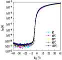
도 7a는 본 발명에 따른 박막 트랜지스터의 신뢰성 측정 결과로서, 물리적인 방법으로 알루미늄 산화물(AlOx)을 증착하여 계면 안정화층을 형성한 경우이다. 온도를 상온에서 100℃로 증가시킨 후에도 문턱전압(Vth), 슬롭 팩터(sub-threshold slop-factor), 오프 전류(off current)가 거의 변화하지 않는 우수한 신뢰성을 나타내었다. 반면, 도 7b는 플라즈마 화학기상증착(PECVD) 방법으로 실리콘 산화물(SiOx)을 증착하여 계면 안정화층을 형성한 경우로서, 온도가 증가함에 따라 문턱전압(Vth)이 음(negative)의 방향으로 변화되고 슬롭 팩터가 열화되었다.FIG. 7A illustrates a reliability measurement result of a thin film transistor according to an exemplary embodiment of the present invention, in which an aluminum oxide (AlOx) is deposited by a physical method to form an interface stabilization layer. Even after increasing the temperature from room temperature to 100 ° C, the threshold voltage (Vth), the sub-threshold slop-factor, the off current (off current) hardly changes the excellent reliability. On the other hand, Figure 7b is a case where the interfacial stabilization layer is formed by depositing silicon oxide (SiOx ) by the plasma chemical vapor deposition (PECVD) method, the threshold voltage (Vth) in the negative direction as the temperature increases Changed and the slop factor deteriorated.
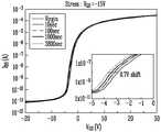
도 8a 및 도 8b는 본 발명에 따른 박막 트랜지스터의 스트레스(stress) 측정 결과로서, 도 8a는 게이트 전극에 15V의 전압(VGS)을 1 시간동안 인가한 경우이고, 도 8b는 게이트 전극에 -15V의 전압(VGS)을 1 시간동안 인가한 경우이다. 도 8a의 경우 0.5V의 문턱전압(Vth) 변화를 나타내었으며, 도 8b의 경우 -0.7V의 문턱전압(Vth) 변화를 나타내었다. 반면, 도 8c는 계면 안정화층을 실리콘 산화물(SiOx)로 형성한 경우로서, 실리콘 산화물(SiOx)은 일반적인 폴리실리콘 박막 트랜지스터 제조에 적용되는 방법으로, 900℃의 온도에서 건식(O2) 또는 습식(H2O) 열산화 방법에 의한 열산화물(SiO2)을 사용하였다. 게이트 전극에 15V의 전압(VGS)을 1 시간동안 인가한 경우 2.1V의 문턱전압(Vth) 변화를, 게이트 전극에 -15V의 전압(VGS)을 1 시간동안 인가한 경우 -2.8V의 문턱전압(Vth) 변화를 나타내었다. 따라서 도 8a 및 도 8b의 결과를 통해 박막 트랜지스터의 신뢰성이 종래에 비해 현저히 개선되었음을 알 수 있다.8A and 8B are stress measurement results of the thin film transistor according to the present invention. FIG. 8A illustrates a case in which a voltage VGS of 15 V is applied to a gate electrode for 1 hour, and FIG. This is the case when a voltage of 15 V (VGS ) is applied for 1 hour. In the case of FIG. 8A, the change in the threshold voltage (Vth) of 0.5V is shown, and in FIG. 8B, the change in the threshold voltage (Vth) of -0.7V is shown. On the other hand,, (SiOx) of silicon oxide as the case in which an interfacial stability layer is an 8c of silicon oxide (SiOx) is a method applied to the common poly manufacturing silicon thin film transistors, and dry at a temperature of 900 ℃ (O2) Or a thermal oxide (SiO2 ) by a wet (H2 O) thermal oxidation method was used. When the voltage VGS of 15 V is applied to the gate electrode for 1 hour, the threshold voltage Vth is changed to 2.1 V. The voltage VGS of -15 V is applied to the gate electrode for 1 hour. The threshold voltage Vth is shown. Therefore, it can be seen from the results of FIGS. 8A and 8B that the reliability of the thin film transistor is remarkably improved compared with the conventional art.
본 발명의 박막 트랜지스터는 평판 표시 장치에 적용될 수 있다. 도 9는 본 발명에 따른 박막 트랜지스터를 구비하는 평판 표시 장치의 일 실시예를 설명하기 위한 사시도로서, 화상을 표시하는 표시 패널(100)을 중심으로 개략적으로 설명한다.The thin film transistor of the present invention can be applied to a flat panel display. FIG. 9 is a perspective view illustrating an exemplary embodiment of a flat panel display device having a thin film transistor according to an exemplary embodiment of the present invention, and will be schematically described with reference to the
표시 패널(100)은 대향하도록 배치된 두 개의 기판(110 및 120)과, 두 개의 기판(110 및 120) 사이에 개재된 액정층(130)으로 이루어지며, 기판(110)에 매트릭스 형태로 배열된 다수의 게이트 선(111)과 데이터 선(112)에 의해 화소 영역(113) 이 정의된다.The
게이트 선(111)과 데이터 선(112)이 교차되는 부분의 기판(110)에는 각 화소로 공급되는 신호를 제어하는 박막 트랜지스터(114) 및 박막 트랜지스터(114)와 연결된 화소 전극(115)이 형성된다. 박막 트랜지스터(114)는 도 1 내지 도 5 중 하나의 구조를 가지며, 도 6a 내지 도 6d를 참조하여 설명한 본 발명의 제조 방법에 따라 제조될 수 있다.A
또한, 기판(120)에는 컬러필터(121) 및 공통전극(122)이 형성된다. 그리고 기판(110 및 120)의 배면에는 편광판(116 및 123)이 각각 형성되며, 편광판(116)의 하부에는 광원으로서 백 라이트(도시안됨)가 배치된다.In addition, the
한편, 표시 패널(100)의 화소 영역(113) 주변에는 표시 패널(100)을 구동시키기 위한 구동부(LCD Drive IC; 도시안됨)가 실장된다. 구동부는 외부로부터 제공되는 전기적 신호를 주사 신호 및 데이터 신호로 변환하여 게이트 선과 데이터 선으로 공급한다.Meanwhile, a driving unit (not shown) for driving the
도 10a 및 도 10b는 본 발명에 따른 박막 트랜지스터를 구비하는 평판 표시 장치의 다른 실시예를 설명하기 위한 평면도 및 단면도로서, 화상을 표시하는 표시 패널(200)을 중심으로 개략적으로 설명한다.10A and 10B are a plan view and a cross-sectional view for describing another exemplary embodiment of a flat panel display including a thin film transistor according to the present invention, and will be schematically described with reference to the
도 10a를 참조하면, 기판(210)은 화소 영역(220)과, 화소 영역(220) 주변의 비화소 영역(230)으로 정의된다. 화소 영역(220)의 기판(210)에는 주사 라인(224) 및 데이터 라인(226) 사이에 매트릭스 방식으로 연결된 다수의 유기전계발광 소자(300)가 형성되고, 비화소 영역(230)의 기판(210)에는 화소 영역(220)의 주사 라 인(224) 및 데이터 라인(226)으로부터 연장된 주사 라인(224) 및 데이터 라인(226), 유기전계발광 소자(300)의 동작을 위한 전원공급 라인(도시안됨) 그리고 패드(228)를 통해 외부로부터 제공된 신호를 처리하여 주사 라인(224) 및 데이터 라인(226)으로 공급하는 주사 구동부(234) 및 데이터 구동부(236)가 형성된다.Referring to FIG. 10A, the
도 11을 참조하면, 유기전계발광 소자(300)는 애노드 전극(317) 및 캐소드 전극(320)과, 애노드 전극(317) 및 캐소드 전극(320) 사이에 형성된 유기 박막층(319)으로 이루어진다. 유기 박막층(319)은 정공 수송층, 유기발광층 및 전자 수송층이 적층된 구조로 형성되며, 정공 주입층과 전자 주입층이 더 포함될 수 있다. 또한, 유기전계발광 소자(300)의 동작을 제어하기 위한 박막 트랜지스터와 신호를 유지시키기 위한 캐패시터가 더 포함될 수 있다.Referring to FIG. 11, the organic light emitting
박막 트랜지스터는 도 1 내지 도 5 중 하나의 구조를 가지며, 도 6a 내지 도 6d를 참조하여 설명한 본 발명의 제조 방법에 따라 제조될 수 있다. 박막 트랜지스터를 포함하는 유기전계발광 소자(300)를 도 10a 및 도 11을 통해 보다 상세히 설명하면 다음과 같다.The thin film transistor has a structure of one of FIGS. 1 to 5 and may be manufactured according to the manufacturing method of the present invention described with reference to FIGS. 6A to 6D. The
기판(210) 상에 버퍼층(41)이 형성되고, 화소 영역(220)의 버퍼층(41) 상에 게이트 전극(42)이 형성된다. 이 때 화소 영역(220)에는 게이트 전극(42)과 연결되는 주사 라인(224)이 형성되고, 비화소 영역(230)에는 화소 영역(220)의 주사 라인(224)으로부터 연장되는 주사 라인(224) 및 외부로부터 신호를 제공받기 위한 패드(228)가 형성될 수 있다.The
게이트 전극(42)을 포함하는 상부에는 게이트 절연층(43)이 형성되고, 게이 트 전극(42)을 포함하는 게이트 절연층(43) 상에는 산화물 반도체로 이루어진 활성층(45)이 형성된다. 활성층(45)의 하부면과 상부면에는 계면 안정화층(44 및 46)이 각각 형성된다.A
활성층(45)의 양측에는 소스 및 드레인 전극(47a 및 47b)이 형성된다. 이 때 화소 영역(220)에는 소스 및 드레인 전극(47a 및 47b)과 연결되는 데이터 라인(226)이 형성되고, 비화소 영역(230)에는 화소 영역(220)의 데이터 라인(226)으로부터 연장되는 데이터 라인(226) 및 외부로부터 신호를 제공받기 위한 패드(228)가 형성될 수 있다.Source and
상기와 같이 구성된 박막 트랜지스터 상부에는 표면 평탄화를 위해 평탄화층(48)이 형성되고, 평탄화층(48)에는 소스 또는 드레인 전극(47a 또는 47b)이 노출되도록 비아홀이 형성된다. 그리고 비아홀을 통해 소스 또는 드레인 전극(47a 또는 47b)과 연결되도록 애노드 전극(317)이 형성된다.The
애노드 전극(317)의 일부 영역(발광 영역)이 노출되도록 평탄화층(48) 상에 화소 정의막(318)이 형성되고, 노출된 애노드 전극(317) 상에 유기 박막층(319)이 형성된다. 유기 박막층(319)을 포함하는 화소 정의막(318) 상에 캐소드 전극(320)이 형성된다.The
도 10b를 참조하면, 상기와 같이 유기전계발광 소자(300)가 형성된 기판(210) 상부에는 화소 영역(220)을 밀봉시키기 위한 봉지 기판(400)이 배치되고, 밀봉재(410)에 의해 봉지 기판(400)이 기판(210)에 합착되어 표시 패널(200)이 완성된다.Referring to FIG. 10B, an
이상에서와 같이 상세한 설명과 도면을 통해 본 발명의 최적 실시예를 개시하였다. 용어들은 단지 본 발명을 설명하기 위한 목적에서 사용된 것이지 의미 한정이나 특허청구범위에 기재된 본 발명의 범위를 제한하기 위하여 사용된 것은 아니다. 그러므로 본 기술 분야의 통상의 지식을 가진 자라면 이로부터 다양한 변형 및 균등한 타 실시예가 가능하다는 점을 이해할 것이다. 따라서 본 발명의 진정한 기술적 보호 범위는 첨부된 특허청구범위의 기술적 사상에 의해 정해져야 할 것이다.As described above, the preferred embodiment of the present invention has been disclosed through the detailed description and the drawings. The terms are used only for the purpose of describing the present invention and are not used to limit the scope of the present invention as defined in the meaning or claims. Therefore, those skilled in the art will understand that various modifications and equivalent other embodiments are possible from this. Therefore, the true technical protection scope of the present invention will be defined by the technical spirit of the appended claims.
도 1은 본 발명의 제 1 실시예에 따른 박막 트랜지스터를 설명하기 위한 단면도.1 is a cross-sectional view illustrating a thin film transistor according to a first embodiment of the present invention.
도 2는 본 발명의 제 2 실시예에 따른 박막 트랜지스터를 설명하기 위한 단면도.2 is a cross-sectional view illustrating a thin film transistor according to a second exemplary embodiment of the present invention.
도 3은 본 발명의 제 3 실시예에 따른 박막 트랜지스터를 설명하기 위한 단면도.3 is a cross-sectional view illustrating a thin film transistor according to a third embodiment of the present invention.
도 4는 본 발명의 제 4 실시예에 따른 박막 트랜지스터를 설명하기 위한 단면도.4 is a cross-sectional view illustrating a thin film transistor according to a fourth embodiment of the present invention.
도 5는 본 발명의 제 5 실시예에 따른 박막 트랜지스터를 설명하기 위한 단면도.5 is a cross-sectional view illustrating a thin film transistor according to a fifth embodiment of the present invention.
도 6a 내지 도 6d는 본 발명에 따른 박막 트랜지스터의 제조 방법을 설명하기 위한 단면도.6A to 6D are cross-sectional views illustrating a method of manufacturing a thin film transistor according to the present invention.
도 7a 및 도 7b는 본 발명에 따른 박막 트랜지스터의 신뢰성 측정 결과를 설명하기 위한 그래프.7A and 7B are graphs for describing the reliability measurement results of the thin film transistor according to the present invention.
도 8a 내지 도 8c는 본 발명에 따른 박막 트랜지스터의 스트레스 측정 결과를 설명하기 위한 그래프.8A to 8C are graphs for explaining the stress measurement results of the thin film transistor according to the present invention.
도 9는 본 발명에 따른 박막 트랜지스터를 구비하는 평판 표시 장치의 일 실시예를 설명하기 위한 사시도.9 is a perspective view for explaining an exemplary embodiment of a flat panel display including a thin film transistor according to the present invention.
도 10a 및 도 10b는 본 발명에 따른 박막 트랜지스터를 구비하는 평판 표시 장치의 다른 실시예를 설명하기 위한 평면도 및 단면도.10A and 10B are a plan view and a sectional view for explaining another embodiment of a flat panel display device having a thin film transistor according to the present invention.
도 11은 도 10a의 유기전계발광 소자를 설명하기 위한 단면도.FIG. 11 is a cross-sectional view for describing the organic light emitting display device of FIG. 10A. FIG.
<도면의 주요 부분에 대한 부호의 설명><Explanation of symbols for the main parts of the drawings>
10, 30, 40, 110, 120, 210: 기판11, 31, 41: 버퍼층10, 30, 40, 110, 120, 210:
12, 32, 42: 게이트 전극13, 33, 43: 게이트 절연층12, 32, 42:
14, 24, 35, 44, 46: 계면 안정화층14, 24, 35, 44, 46: interfacial stabilization layer
15, 34, 45: 산화물 반도체층15a, 34a, 45a: 채널 영역15, 34, 45:
15b, 34b, 45b: 소스 영역15c, 34c, 45c: 드레인 영역15b, 34b, 45b:
16a, 36a, 47a: 소스 전극16b, 36b, 47b: 드레인 전극16a, 36a, 47a:
26: 보호층48: 평탄화층26: protective layer 48: planarization layer
100, 200: 표시 패널111: 게이트 선100, 200: display panel 111: gate line
112: 데이터 선113: 화소 영역112: data line 113: pixel area
114: 박막 트랜지스터115: 화소 전극114: thin film transistor 115: pixel electrode
116, 123: 편광판121: 컬러필터116, 123: polarizer 121: color filter
122: 공통전극130: 액정층122: common electrode 130: liquid crystal layer
220: 화소 영역224: 주사 라인220: pixel region 224: scan line
226: 데이터 라인228: 패드226: data line 228: pad
230: 비화소 영역234: 주사 구동부230: non-pixel region 234: scan driver
236: 데이터 구동부300: 유기전계발광 소자236: data driver 300: organic light emitting device
317: 애노드 전극318: 화소 정의막317: anode electrode 318: pixel defining film
319: 유기 박막층320: 캐소드 전극319: organic thin film layer 320: cathode electrode
400: 봉지 기판410: 밀봉재400: sealing substrate 410: sealing material
Claims (39)
Translated fromKoreanPriority Applications (6)
| Application Number | Priority Date | Filing Date | Title |
|---|---|---|---|
| KR1020080062418AKR100963027B1 (en) | 2008-06-30 | 2008-06-30 | Thin film transistor, its manufacturing method, and flat panel display device comprising thin film transistor |
| US12/352,851US8148779B2 (en) | 2008-06-30 | 2009-01-13 | Thin film transistor, method of manufacturing the same and flat panel display device having the same |
| JP2009046233AJP5474374B2 (en) | 2008-06-30 | 2009-02-27 | THIN FILM TRANSISTOR, ITS MANUFACTURING METHOD, AND FLAT DISPLAY DEVICE PROVIDED WITH THIN FILM TRANSISTOR |
| EP20090250845EP2141743A1 (en) | 2008-06-30 | 2009-03-25 | Thin film transistor, method of manufacturing the same and flat panel display device having the same |
| CN200910137879.3ACN101621075B (en) | 2008-06-30 | 2009-05-05 | Thin film transistor, method of manufacturing the same and flat panel display device having the same |
| US13/408,825US9035313B2 (en) | 2008-06-30 | 2012-02-29 | Thin film transistor, method of manufacturing the same and flat panel display device having the same |
Applications Claiming Priority (1)
| Application Number | Priority Date | Filing Date | Title |
|---|---|---|---|
| KR1020080062418AKR100963027B1 (en) | 2008-06-30 | 2008-06-30 | Thin film transistor, its manufacturing method, and flat panel display device comprising thin film transistor |
Publications (2)
| Publication Number | Publication Date |
|---|---|
| KR20100002504A KR20100002504A (en) | 2010-01-07 |
| KR100963027B1true KR100963027B1 (en) | 2010-06-10 |
Family
ID=40765468
Family Applications (1)
| Application Number | Title | Priority Date | Filing Date |
|---|---|---|---|
| KR1020080062418AActiveKR100963027B1 (en) | 2008-06-30 | 2008-06-30 | Thin film transistor, its manufacturing method, and flat panel display device comprising thin film transistor |
Country Status (5)
| Country | Link |
|---|---|
| US (2) | US8148779B2 (en) |
| EP (1) | EP2141743A1 (en) |
| JP (1) | JP5474374B2 (en) |
| KR (1) | KR100963027B1 (en) |
| CN (1) | CN101621075B (en) |
Cited By (1)
| Publication number | Priority date | Publication date | Assignee | Title |
|---|---|---|---|---|
| KR101318418B1 (en)* | 2012-01-30 | 2013-10-15 | 서울대학교산학협력단 | Thin film transistor and the manufacturing method thereof |
Families Citing this family (295)
| Publication number | Priority date | Publication date | Assignee | Title |
|---|---|---|---|---|
| KR100963027B1 (en) | 2008-06-30 | 2010-06-10 | 삼성모바일디스플레이주식회사 | Thin film transistor, its manufacturing method, and flat panel display device comprising thin film transistor |
| KR100963026B1 (en)* | 2008-06-30 | 2010-06-10 | 삼성모바일디스플레이주식회사 | Thin film transistor, its manufacturing method, and flat panel display device comprising thin film transistor |
| JP5345456B2 (en)* | 2008-08-14 | 2013-11-20 | 富士フイルム株式会社 | Thin film field effect transistor |
| JP5339825B2 (en)* | 2008-09-09 | 2013-11-13 | 富士フイルム株式会社 | Thin film field effect transistor and display device using the same |
| KR101657957B1 (en)* | 2008-09-12 | 2016-09-20 | 가부시키가이샤 한도오따이 에네루기 켄큐쇼 | Display device |
| JP5345359B2 (en)* | 2008-09-18 | 2013-11-20 | 富士フイルム株式会社 | Thin film field effect transistor and display device using the same |
| JP5442234B2 (en) | 2008-10-24 | 2014-03-12 | 株式会社半導体エネルギー研究所 | Semiconductor device and display device |
| TWI567829B (en) | 2008-10-31 | 2017-01-21 | 半導體能源研究所股份有限公司 | Semiconductor device and method of manufacturing same |
| TWI506795B (en) | 2008-11-28 | 2015-11-01 | Semiconductor Energy Lab | Semiconductor device and method of manufacturing same |
| KR101648927B1 (en) | 2009-01-16 | 2016-08-17 | 가부시키가이샤 한도오따이 에네루기 켄큐쇼 | Semiconductor device and manufacturing method thereof |
| JP5371467B2 (en)* | 2009-02-12 | 2013-12-18 | 富士フイルム株式会社 | FIELD EFFECT TRANSISTOR AND METHOD FOR MANUFACTURING FIELD EFFECT TRANSISTOR |
| JP5504008B2 (en) | 2009-03-06 | 2014-05-28 | 株式会社半導体エネルギー研究所 | Semiconductor device |
| TWI535023B (en)* | 2009-04-16 | 2016-05-21 | 半導體能源研究所股份有限公司 | Semiconductor device and method of manufacturing same |
| EP2256814B1 (en) | 2009-05-29 | 2019-01-16 | Semiconductor Energy Laboratory Co, Ltd. | Oxide semiconductor device and method for manufacturing the same |
| KR101799252B1 (en) | 2009-07-31 | 2017-11-17 | 가부시키가이샤 한도오따이 에네루기 켄큐쇼 | Semiconductor device and method for manufacturing the same |
| KR102097932B1 (en) | 2009-07-31 | 2020-04-06 | 가부시키가이샤 한도오따이 에네루기 켄큐쇼 | Semiconductor device and manufacturing method thereof |
| WO2011013523A1 (en) | 2009-07-31 | 2011-02-03 | Semiconductor Energy Laboratory Co., Ltd. | Semiconductor device and method for manufacturing the same |
| WO2011013596A1 (en) | 2009-07-31 | 2011-02-03 | Semiconductor Energy Laboratory Co., Ltd. | Semiconductor device and manufacturing method thereof |
| WO2011013502A1 (en) | 2009-07-31 | 2011-02-03 | Semiconductor Energy Laboratory Co., Ltd. | Semiconductor device and manufacturing method thereof |
| KR101073543B1 (en)* | 2009-09-04 | 2011-10-17 | 삼성모바일디스플레이주식회사 | Organic light emitting diode display |
| TW202507679A (en)* | 2009-09-10 | 2025-02-16 | 日商半導體能源研究所股份有限公司 | Semiconductor device and display device |
| KR20230165355A (en)* | 2009-09-16 | 2023-12-05 | 가부시키가이샤 한도오따이 에네루기 켄큐쇼 | Display device |
| CN102511082B (en)* | 2009-09-16 | 2016-04-27 | 株式会社半导体能源研究所 | Semiconductor device and manufacturing method thereof |
| KR20190045396A (en)* | 2009-09-16 | 2019-05-02 | 가부시키가이샤 한도오따이 에네루기 켄큐쇼 | Transistor |
| KR102219095B1 (en)* | 2009-09-24 | 2021-02-23 | 가부시키가이샤 한도오따이 에네루기 켄큐쇼 | Semiconductor device and method for manufacturing the same |
| KR20220127372A (en) | 2009-09-24 | 2022-09-19 | 가부시키가이샤 한도오따이 에네루기 켄큐쇼 | Oxide semiconductor film and semiconductor device |
| WO2011043206A1 (en) | 2009-10-09 | 2011-04-14 | Semiconductor Energy Laboratory Co., Ltd. | Semiconductor device |
| CN105702688B (en) | 2009-10-21 | 2020-09-08 | 株式会社半导体能源研究所 | Liquid crystal display device and electronic apparatus including the same |
| SG10201406869QA (en)* | 2009-10-29 | 2014-12-30 | Semiconductor Energy Lab | Semiconductor device |
| WO2011052384A1 (en) | 2009-10-30 | 2011-05-05 | Semiconductor Energy Laboratory Co., Ltd. | Semiconductor device and method for manufacturing the same |
| CN102687400B (en) | 2009-10-30 | 2016-08-24 | 株式会社半导体能源研究所 | Logic circuit and semiconductor device |
| KR101849321B1 (en) | 2009-11-06 | 2018-04-16 | 가부시키가이샤 한도오따이 에네루기 켄큐쇼 | Semiconductor device and manufacturing method thereof |
| KR101652790B1 (en)* | 2009-11-09 | 2016-08-31 | 삼성전자주식회사 | Transistor, method of manufacturing the same and electronic device comprising transistor |
| KR101638977B1 (en)* | 2009-11-13 | 2016-07-12 | 삼성전자주식회사 | Transistor, method of manufacturing the same and electronic device comprising transistor |
| WO2011065210A1 (en) | 2009-11-28 | 2011-06-03 | Semiconductor Energy Laboratory Co., Ltd. | Stacked oxide material, semiconductor device, and method for manufacturing the semiconductor device |
| WO2011065243A1 (en) | 2009-11-28 | 2011-06-03 | Semiconductor Energy Laboratory Co., Ltd. | Semiconductor device and manufacturing method thereof |
| KR101825345B1 (en) | 2009-11-28 | 2018-02-05 | 가부시키가이샤 한도오따이 에네루기 켄큐쇼 | Stacked oxide material, semiconductor device, and method for manufacturing the semiconductor device |
| WO2011065244A1 (en) | 2009-11-28 | 2011-06-03 | Semiconductor Energy Laboratory Co., Ltd. | Semiconductor device and method for manufacturing the same |
| KR102250803B1 (en) | 2009-12-04 | 2021-05-11 | 가부시키가이샤 한도오따이 에네루기 켄큐쇼 | Semiconductor device |
| KR102719739B1 (en) | 2009-12-04 | 2024-10-21 | 가부시키가이샤 한도오따이 에네루기 켄큐쇼 | Semiconductor device |
| KR102241766B1 (en) | 2009-12-04 | 2021-04-19 | 가부시키가이샤 한도오따이 에네루기 켄큐쇼 | Semiconductor device and manufacturing method thereof |
| KR101945171B1 (en) | 2009-12-08 | 2019-02-07 | 가부시키가이샤 한도오따이 에네루기 켄큐쇼 | Semiconductor device |
| WO2011070929A1 (en) | 2009-12-11 | 2011-06-16 | Semiconductor Energy Laboratory Co., Ltd. | Semiconductor device and electronic device |
| KR101768433B1 (en) | 2009-12-18 | 2017-08-16 | 가부시키가이샤 한도오따이 에네루기 켄큐쇼 | Method for manufacturing semiconductor device |
| KR101613701B1 (en)* | 2009-12-25 | 2016-04-19 | 가부시키가이샤 한도오따이 에네루기 켄큐쇼 | Method for driving liquid crystal display device |
| CN103985760B (en) | 2009-12-25 | 2017-07-18 | 株式会社半导体能源研究所 | Semiconductor device |
| CN102903758B (en)* | 2009-12-28 | 2015-06-03 | 株式会社半导体能源研究所 | Semiconductor device |
| WO2011086905A1 (en)* | 2010-01-13 | 2011-07-21 | シャープ株式会社 | Active matrix substrate and manufacturing method thereof |
| KR101701208B1 (en)* | 2010-01-15 | 2017-02-02 | 삼성디스플레이 주식회사 | Display substrate |
| US8780629B2 (en) | 2010-01-15 | 2014-07-15 | Semiconductor Energy Laboratory Co., Ltd. | Semiconductor device and driving method thereof |
| KR102129540B1 (en) | 2010-01-20 | 2020-07-03 | 가부시키가이샤 한도오따이 에네루기 켄큐쇼 | Display device |
| KR20190093706A (en) | 2010-01-24 | 2019-08-09 | 가부시키가이샤 한도오따이 에네루기 켄큐쇼 | Display device and manufacturing method thereof |
| JP2011155061A (en)* | 2010-01-26 | 2011-08-11 | Sony Corp | Thin film transistor, method of manufacturing the same, display device, and electronic apparatus |
| KR20180006507A (en) | 2010-02-05 | 2018-01-17 | 가부시키가이샤 한도오따이 에네루기 켄큐쇼 | Semiconductor device and method for manufacturing the same |
| KR20110093113A (en)* | 2010-02-11 | 2011-08-18 | 삼성전자주식회사 | Thin film transistor substrate and manufacturing method thereof |
| CN105336744B (en) | 2010-02-12 | 2018-12-21 | 株式会社半导体能源研究所 | Semiconductor device and its driving method |
| JP2011188733A (en)* | 2010-02-12 | 2011-09-22 | Semiconductor Energy Lab Co Ltd | Moving object, and system and method for wireless power feeding |
| KR101636998B1 (en)* | 2010-02-12 | 2016-07-08 | 삼성디스플레이 주식회사 | Thin Film Transistor and Method to Fabricate the Same |
| KR101627136B1 (en)* | 2010-02-19 | 2016-06-07 | 삼성디스플레이 주식회사 | Thin film transistor substrate, method of manufacturing the same and display device comprising the same |
| KR101117737B1 (en) | 2010-03-02 | 2012-02-24 | 삼성모바일디스플레이주식회사 | Organic light emitting display apparatus |
| KR101878206B1 (en)* | 2010-03-05 | 2018-07-16 | 가부시키가이샤 한도오따이 에네루기 켄큐쇼 | Manufacturing method of oxide semiconductor film and manufacturing method of transistor |
| WO2011118741A1 (en) | 2010-03-26 | 2011-09-29 | Semiconductor Energy Laboratory Co., Ltd. | Method for manufacturing semiconductor device |
| CN102822980B (en) | 2010-03-26 | 2015-12-16 | 株式会社半导体能源研究所 | Manufacturing method of semiconductor device |
| CN102834921B (en) | 2010-03-26 | 2016-04-27 | 株式会社半导体能源研究所 | Manufacturing method of semiconductor device |
| JP5727832B2 (en)* | 2010-03-31 | 2015-06-03 | 株式会社半導体エネルギー研究所 | Transistor |
| US9147768B2 (en) | 2010-04-02 | 2015-09-29 | Semiconductor Energy Laboratory Co., Ltd. | Semiconductor device having an oxide semiconductor and a metal oxide film |
| US9196739B2 (en) | 2010-04-02 | 2015-11-24 | Semiconductor Energy Laboratory Co., Ltd. | Semiconductor device including oxide semiconductor film and metal oxide film |
| KR102276768B1 (en)* | 2010-04-02 | 2021-07-13 | 가부시키가이샤 한도오따이 에네루기 켄큐쇼 | Semiconductor device |
| KR102436902B1 (en) | 2010-04-02 | 2022-08-25 | 가부시키가이샤 한도오따이 에네루기 켄큐쇼 | Semiconductor device |
| US8884282B2 (en) | 2010-04-02 | 2014-11-11 | Semiconductor Energy Laboratory Co., Ltd. | Semiconductor device |
| US9190522B2 (en) | 2010-04-02 | 2015-11-17 | Semiconductor Energy Laboratory Co., Ltd. | Semiconductor device having an oxide semiconductor |
| KR101803730B1 (en) | 2010-04-09 | 2017-12-01 | 가부시키가이샤 한도오따이 에네루기 켄큐쇼 | Semiconductor device |
| US8653514B2 (en) | 2010-04-09 | 2014-02-18 | Semiconductor Energy Laboratory Co., Ltd. | Semiconductor device and method for manufacturing the same |
| CN102844847B (en) | 2010-04-16 | 2015-09-23 | 株式会社半导体能源研究所 | The manufacture method of deposition process and semiconductor device |
| KR20130045418A (en) | 2010-04-23 | 2013-05-03 | 가부시키가이샤 한도오따이 에네루기 켄큐쇼 | Manufacturing method of semiconductor device |
| KR101754380B1 (en) | 2010-04-23 | 2017-07-05 | 가부시키가이샤 한도오따이 에네루기 켄큐쇼 | Method for manufacturing semiconductor device |
| KR101324760B1 (en)* | 2010-04-23 | 2013-11-05 | 가부시키가이샤 한도오따이 에네루기 켄큐쇼 | Method for manufacturing semiconductor device |
| KR102434906B1 (en)* | 2010-04-23 | 2022-08-23 | 가부시키가이샤 한도오따이 에네루기 켄큐쇼 | Method for manufacturing semiconductor device |
| WO2011132591A1 (en) | 2010-04-23 | 2011-10-27 | Semiconductor Energy Laboratory Co., Ltd. | Method for manufacturing semiconductor device |
| CN105390402B (en)* | 2010-04-23 | 2018-09-07 | 株式会社半导体能源研究所 | The manufacturing method of semiconductor device and semiconductor device |
| WO2011135987A1 (en)* | 2010-04-28 | 2011-11-03 | Semiconductor Energy Laboratory Co., Ltd. | Method for manufacturing semiconductor device |
| KR101806271B1 (en) | 2010-05-14 | 2017-12-07 | 가부시키가이샤 한도오따이 에네루기 켄큐쇼 | Method for manufacturing semiconductor device |
| JP5606787B2 (en)* | 2010-05-18 | 2014-10-15 | 富士フイルム株式会社 | Thin film transistor manufacturing method, thin film transistor, image sensor, X-ray sensor, and X-ray digital imaging apparatus |
| US8629438B2 (en) | 2010-05-21 | 2014-01-14 | Semiconductor Energy Laboratory Co., Ltd. | Semiconductor device and manufacturing method thereof |
| WO2011155295A1 (en) | 2010-06-10 | 2011-12-15 | Semiconductor Energy Laboratory Co., Ltd. | Dc/dc converter, power supply circuit, and semiconductor device |
| WO2011155302A1 (en) | 2010-06-11 | 2011-12-15 | Semiconductor Energy Laboratory Co., Ltd. | Semiconductor device |
| US9209314B2 (en) | 2010-06-16 | 2015-12-08 | Semiconductor Energy Laboratory Co., Ltd. | Field effect transistor |
| KR101862808B1 (en)* | 2010-06-18 | 2018-05-30 | 가부시키가이샤 한도오따이 에네루기 켄큐쇼 | Semiconductor device |
| WO2011158704A1 (en) | 2010-06-18 | 2011-12-22 | Semiconductor Energy Laboratory Co., Ltd. | Method for manufacturing semiconductor device |
| US8552425B2 (en)* | 2010-06-18 | 2013-10-08 | Semiconductor Energy Laboratory Co., Ltd. | Semiconductor device |
| WO2012002040A1 (en) | 2010-07-01 | 2012-01-05 | Semiconductor Energy Laboratory Co., Ltd. | Driving method of liquid crystal display device |
| JP2013531383A (en)* | 2010-07-02 | 2013-08-01 | ヒューレット−パッカード デベロップメント カンパニー エル.ピー. | Thin film transistor |
| KR101995851B1 (en)* | 2010-07-02 | 2019-07-03 | 가부시키가이샤 한도오따이 에네루기 켄큐쇼 | Semiconductor device |
| WO2012002186A1 (en) | 2010-07-02 | 2012-01-05 | Semiconductor Energy Laboratory Co., Ltd. | Semiconductor device |
| US9246010B2 (en)* | 2010-07-14 | 2016-01-26 | Sharp Kabushiki Kaisha | Thin film transistor substrate |
| KR101671952B1 (en)* | 2010-07-23 | 2016-11-04 | 삼성디스플레이 주식회사 | Display substrate and method of manufacturing the same |
| KR101108178B1 (en)* | 2010-07-27 | 2012-01-31 | 삼성모바일디스플레이주식회사 | Thin Film Transistor Sensor and Thin Film Transistor Manufacturing Method |
| JP5832181B2 (en) | 2010-08-06 | 2015-12-16 | 株式会社半導体エネルギー研究所 | Liquid crystal display |
| KR101774992B1 (en)* | 2010-08-10 | 2017-09-06 | 삼성디스플레이 주식회사 | Display substrate and method of manufacturing the same |
| US9058047B2 (en) | 2010-08-26 | 2015-06-16 | Semiconductor Energy Laboratory Co., Ltd. | Semiconductor device |
| JP5806043B2 (en) | 2010-08-27 | 2015-11-10 | 株式会社半導体エネルギー研究所 | Method for manufacturing semiconductor device |
| US8835917B2 (en) | 2010-09-13 | 2014-09-16 | Semiconductor Energy Laboratory Co., Ltd. | Semiconductor device, power diode, and rectifier |
| US8647919B2 (en) | 2010-09-13 | 2014-02-11 | Semiconductor Energy Laboratory Co., Ltd. | Light-emitting display device and method for manufacturing the same |
| US8558960B2 (en) | 2010-09-13 | 2013-10-15 | Semiconductor Energy Laboratory Co., Ltd. | Liquid crystal display device and method for manufacturing the same |
| KR101932576B1 (en) | 2010-09-13 | 2018-12-26 | 가부시키가이샤 한도오따이 에네루기 켄큐쇼 | Semiconductor device and method for manufacturing the same |
| KR20180124158A (en) | 2010-09-15 | 2018-11-20 | 가부시키가이샤 한도오따이 에네루기 켄큐쇼 | Liquid crystal display device and manufacturing method thereof |
| TWI556317B (en) | 2010-10-07 | 2016-11-01 | 半導體能源研究所股份有限公司 | Thin film element, semiconductor device, and method of manufacturing same |
| US8936965B2 (en) | 2010-11-26 | 2015-01-20 | Semiconductor Energy Laboratory Co., Ltd. | Semiconductor device and manufacturing method thereof |
| US8809852B2 (en) | 2010-11-30 | 2014-08-19 | Semiconductor Energy Laboratory Co., Ltd. | Semiconductor film, semiconductor element, semiconductor device, and method for manufacturing the same |
| TWI562379B (en) | 2010-11-30 | 2016-12-11 | Semiconductor Energy Lab Co Ltd | Semiconductor device and method for manufacturing semiconductor device |
| JP5723262B2 (en)* | 2010-12-02 | 2015-05-27 | 株式会社神戸製鋼所 | Thin film transistor and sputtering target |
| CN103500712B (en) | 2010-12-03 | 2016-05-25 | 株式会社半导体能源研究所 | Semiconductor device |
| US9024317B2 (en) | 2010-12-24 | 2015-05-05 | Semiconductor Energy Laboratory Co., Ltd. | Semiconductor circuit, method for driving the same, storage device, register circuit, display device, and electronic device |
| US8921948B2 (en) | 2011-01-12 | 2014-12-30 | Semiconductor Energy Laboratory Co., Ltd. | Semiconductor device and manufacturing method thereof |
| US8536571B2 (en) | 2011-01-12 | 2013-09-17 | Semiconductor Energy Laboratory Co., Ltd. | Manufacturing method of semiconductor device |
| TWI535032B (en) | 2011-01-12 | 2016-05-21 | 半導體能源研究所股份有限公司 | Semiconductor device manufacturing method |
| KR101942701B1 (en)* | 2011-01-20 | 2019-01-29 | 가부시키가이샤 한도오따이 에네루기 켄큐쇼 | Oxide semiconductor element and semiconductor device |
| KR102233959B1 (en) | 2011-01-28 | 2021-03-29 | 가부시키가이샤 한도오따이 에네루기 켄큐쇼 | Method for manufacturing semiconductor device and semiconductor device |
| TWI521612B (en) | 2011-03-11 | 2016-02-11 | 半導體能源研究所股份有限公司 | Semiconductor device manufacturing method |
| TWI624878B (en) | 2011-03-11 | 2018-05-21 | 半導體能源研究所股份有限公司 | Semiconductor device manufacturing method |
| JP5615744B2 (en)* | 2011-03-14 | 2014-10-29 | 富士フイルム株式会社 | FIELD EFFECT TRANSISTOR, DISPLAY DEVICE, SENSOR, AND METHOD FOR MANUFACTURING FIELD EFFECT TRANSISTOR |
| US9082860B2 (en)* | 2011-03-31 | 2015-07-14 | Semiconductor Energy Laboratory Co., Ltd. | Semiconductor device |
| US8541266B2 (en) | 2011-04-01 | 2013-09-24 | Semiconductor Energy Laboratory Co., Ltd. | Method for manufacturing semiconductor device |
| US9960278B2 (en) | 2011-04-06 | 2018-05-01 | Yuhei Sato | Manufacturing method of semiconductor device |
| US8709922B2 (en) | 2011-05-06 | 2014-04-29 | Semiconductor Energy Laboratory Co., Ltd. | Semiconductor device |
| JP2012238763A (en)* | 2011-05-12 | 2012-12-06 | Fujitsu Ltd | Semiconductor device and method of manufacturing semiconductor device |
| US8581625B2 (en) | 2011-05-19 | 2013-11-12 | Semiconductor Energy Laboratory Co., Ltd. | Programmable logic device |
| CN102789808B (en) | 2011-05-20 | 2018-03-06 | 株式会社半导体能源研究所 | Storage arrangement and the method for driving storage arrangement |
| US8901554B2 (en) | 2011-06-17 | 2014-12-02 | Semiconductor Energy Laboratory Co., Ltd. | Semiconductor device including channel formation region including oxide semiconductor |
| KR20130007426A (en) | 2011-06-17 | 2013-01-18 | 가부시키가이샤 한도오따이 에네루기 켄큐쇼 | Semiconductor device and manufacturing method thereof |
| US9166055B2 (en) | 2011-06-17 | 2015-10-20 | Semiconductor Energy Laboratory Co., Ltd. | Semiconductor device and method for manufacturing the same |
| US8952377B2 (en) | 2011-07-08 | 2015-02-10 | Semiconductor Energy Laboratory Co., Ltd. | Semiconductor device and manufacturing method thereof |
| US9385238B2 (en) | 2011-07-08 | 2016-07-05 | Semiconductor Energy Laboratory Co., Ltd. | Transistor using oxide semiconductor |
| US9252279B2 (en)* | 2011-08-31 | 2016-02-02 | Semiconductor Energy Laboratory Co., Ltd. | Semiconductor device and manufacturing method thereof |
| US9660092B2 (en) | 2011-08-31 | 2017-05-23 | Semiconductor Energy Laboratory Co., Ltd. | Oxide semiconductor thin film transistor including oxygen release layer |
| KR102108572B1 (en) | 2011-09-26 | 2020-05-07 | 가부시키가이샤 한도오따이 에네루기 켄큐쇼 | Semiconductor device and method for manufacturing the same |
| KR102504604B1 (en) | 2011-09-29 | 2023-02-27 | 가부시키가이샤 한도오따이 에네루기 켄큐쇼 | Semiconductor device |
| US20130087784A1 (en) | 2011-10-05 | 2013-04-11 | Semiconductor Energy Laboratory Co., Ltd. | Semiconductor device and manufacturing method thereof |
| US8728861B2 (en)* | 2011-10-12 | 2014-05-20 | The United States Of America As Represented By The Secretary Of The Air Force | Fabrication method for ZnO thin film transistors using etch-stop layer |
| KR20130040706A (en) | 2011-10-14 | 2013-04-24 | 가부시키가이샤 한도오따이 에네루기 켄큐쇼 | Semiconductor device and method of manufacturing semiconductor device |
| WO2013054933A1 (en) | 2011-10-14 | 2013-04-18 | Semiconductor Energy Laboratory Co., Ltd. | Semiconductor device |
| JP6082562B2 (en) | 2011-10-27 | 2017-02-15 | 株式会社半導体エネルギー研究所 | Semiconductor device |
| KR20130046357A (en) | 2011-10-27 | 2013-05-07 | 가부시키가이샤 한도오따이 에네루기 켄큐쇼 | Semiconductor device |
| US9082861B2 (en)* | 2011-11-11 | 2015-07-14 | Semiconductor Energy Laboratory Co., Ltd. | Transistor with oxide semiconductor channel having protective layer |
| JP6076038B2 (en) | 2011-11-11 | 2017-02-08 | 株式会社半導体エネルギー研究所 | Method for manufacturing display device |
| JP6122275B2 (en) | 2011-11-11 | 2017-04-26 | 株式会社半導体エネルギー研究所 | Display device |
| US8829528B2 (en) | 2011-11-25 | 2014-09-09 | Semiconductor Energy Laboratory Co., Ltd. | Semiconductor device including groove portion extending beyond pixel electrode |
| CN103137701B (en)* | 2011-11-30 | 2018-01-19 | 株式会社半导体能源研究所 | Transistor and semiconductor device |
| TWI497689B (en) | 2011-12-02 | 2015-08-21 | Ind Tech Res Inst | Semiconductor component and method of manufacturing same |
| US9236494B2 (en) | 2011-12-13 | 2016-01-12 | E Ink Holdings Inc. | Field effect transistor |
| TWI588997B (en)* | 2011-12-13 | 2017-06-21 | 元太科技工業股份有限公司 | Field effect transistor |
| US8748240B2 (en) | 2011-12-22 | 2014-06-10 | Semiconductor Energy Laboratory Co., Ltd. | Method for manufacturing semiconductor device |
| JP6033071B2 (en) | 2011-12-23 | 2016-11-30 | 株式会社半導体エネルギー研究所 | Semiconductor device |
| TWI613824B (en) | 2011-12-23 | 2018-02-01 | 半導體能源研究所股份有限公司 | Semiconductor device |
| KR101942980B1 (en) | 2012-01-17 | 2019-01-29 | 삼성디스플레이 주식회사 | Semiconductor device and method for forming the same |
| KR102034911B1 (en) | 2012-01-25 | 2019-10-21 | 가부시키가이샤 한도오따이 에네루기 켄큐쇼 | Semiconductor device and method for manufacturing semiconductor device |
| TWI604609B (en) | 2012-02-02 | 2017-11-01 | 半導體能源研究所股份有限公司 | Semiconductor device |
| TWI512840B (en)* | 2012-02-14 | 2015-12-11 | Innocom Tech Shenzhen Co Ltd | Thin film transistor, manufacturing method thereof and display |
| TWI451575B (en)* | 2012-02-16 | 2014-09-01 | E Ink Holdings Inc | Thin film transistor |
| US20130221345A1 (en) | 2012-02-28 | 2013-08-29 | Semiconductor Energy Laboratory Co., Ltd. | Semiconductor device and method for manufacturing the same |
| KR101963226B1 (en)* | 2012-02-29 | 2019-04-01 | 삼성전자주식회사 | Transistor, method of manufacturing the same and electronic device including transistor |
| KR101947808B1 (en)* | 2012-02-29 | 2019-04-25 | 엘지디스플레이 주식회사 | Thin film transistor array substrate and method for manufacturing of the same |
| KR20230004930A (en) | 2012-04-13 | 2023-01-06 | 가부시키가이샤 한도오따이 에네루기 켄큐쇼 | Semiconductor device |
| JP6143423B2 (en) | 2012-04-16 | 2017-06-07 | 株式会社半導体エネルギー研究所 | Manufacturing method of semiconductor device |
| US9219164B2 (en) | 2012-04-20 | 2015-12-22 | Semiconductor Energy Laboratory Co., Ltd. | Semiconductor device with oxide semiconductor channel |
| US9048323B2 (en) | 2012-04-30 | 2015-06-02 | Semiconductor Energy Laboratory Co., Ltd. | Semiconductor device |
| CN104380473B (en) | 2012-05-31 | 2017-10-13 | 株式会社半导体能源研究所 | Semiconductor device |
| US9048265B2 (en) | 2012-05-31 | 2015-06-02 | Semiconductor Energy Laboratory Co., Ltd. | Method for manufacturing semiconductor device comprising oxide semiconductor layer |
| KR102119914B1 (en) | 2012-05-31 | 2020-06-05 | 가부시키가이샤 한도오따이 에네루기 켄큐쇼 | Semiconductor device and manufacturing method thereof |
| JP6208469B2 (en) | 2012-05-31 | 2017-10-04 | 株式会社半導体エネルギー研究所 | Semiconductor device |
| KR102113160B1 (en)* | 2012-06-15 | 2020-05-20 | 가부시키가이샤 한도오따이 에네루기 켄큐쇼 | Semiconductor device |
| US8901557B2 (en) | 2012-06-15 | 2014-12-02 | Semiconductor Energy Laboratory Co., Ltd. | Semiconductor device |
| US9059219B2 (en) | 2012-06-27 | 2015-06-16 | Semiconductor Energy Laboratory Co., Ltd. | Semiconductor device and method for manufacturing semiconductor device |
| KR102161077B1 (en) | 2012-06-29 | 2020-09-29 | 가부시키가이샤 한도오따이 에네루기 켄큐쇼 | Semiconductor device |
| JP6310194B2 (en) | 2012-07-06 | 2018-04-11 | 株式会社半導体エネルギー研究所 | Semiconductor device |
| CN103545307A (en)* | 2012-07-13 | 2014-01-29 | 群康科技(深圳)有限公司 | Display device and display panel thereof |
| JP6134598B2 (en) | 2012-08-02 | 2017-05-24 | 株式会社半導体エネルギー研究所 | Semiconductor device |
| WO2014021442A1 (en) | 2012-08-03 | 2014-02-06 | Semiconductor Energy Laboratory Co., Ltd. | Oxide semiconductor stacked film and semiconductor device |
| WO2014024808A1 (en) | 2012-08-10 | 2014-02-13 | Semiconductor Energy Laboratory Co., Ltd. | Semiconductor device and manufacturing method thereof |
| JP6220597B2 (en) | 2012-08-10 | 2017-10-25 | 株式会社半導体エネルギー研究所 | Semiconductor device |
| US9245958B2 (en) | 2012-08-10 | 2016-01-26 | Semiconductor Energy Laboratory Co., Ltd. | Semiconductor device and method for manufacturing the same |
| CN104584229B (en) | 2012-08-10 | 2018-05-15 | 株式会社半导体能源研究所 | Semiconductor device and manufacturing method thereof |
| US9929276B2 (en) | 2012-08-10 | 2018-03-27 | Semiconductor Energy Laboratory Co., Ltd. | Semiconductor device and method for manufacturing the same |
| US8981372B2 (en) | 2012-09-13 | 2015-03-17 | Semiconductor Energy Laboratory Co., Ltd. | Display device and electronic appliance |
| US9018624B2 (en) | 2012-09-13 | 2015-04-28 | Semiconductor Energy Laboratory Co., Ltd. | Display device and electronic appliance |
| TWI470810B (en) | 2012-09-21 | 2015-01-21 | E Ink Holdings Inc | Thin film transistor, array substrate and display device |
| TW202431646A (en) | 2012-09-24 | 2024-08-01 | 日商半導體能源研究所股份有限公司 | Semiconductor device |
| WO2014046222A1 (en) | 2012-09-24 | 2014-03-27 | Semiconductor Energy Laboratory Co., Ltd. | Display device |
| KR102009017B1 (en)* | 2012-09-28 | 2019-10-23 | 엘지디스플레이 주식회사 | Oxide thin film transistor for display device and method for fabricating the same |
| JP6351947B2 (en) | 2012-10-12 | 2018-07-04 | 株式会社半導体エネルギー研究所 | Method for manufacturing liquid crystal display device |
| TWI681233B (en) | 2012-10-12 | 2020-01-01 | 日商半導體能源研究所股份有限公司 | Liquid crystal display device, touch panel and method for manufacturing liquid crystal display device |
| WO2014061535A1 (en) | 2012-10-17 | 2014-04-24 | Semiconductor Energy Laboratory Co., Ltd. | Semiconductor device |
| JP6021586B2 (en) | 2012-10-17 | 2016-11-09 | 株式会社半導体エネルギー研究所 | Semiconductor device |
| JP5951442B2 (en) | 2012-10-17 | 2016-07-13 | 株式会社半導体エネルギー研究所 | Semiconductor device |
| US9166021B2 (en) | 2012-10-17 | 2015-10-20 | Semiconductor Energy Laboratory Co., Ltd. | Semiconductor device and method for manufacturing the same |
| WO2014061567A1 (en) | 2012-10-17 | 2014-04-24 | Semiconductor Energy Laboratory Co., Ltd. | Programmable logic device |
| JP2014082388A (en) | 2012-10-17 | 2014-05-08 | Semiconductor Energy Lab Co Ltd | Semiconductor device |
| JP6283191B2 (en) | 2012-10-17 | 2018-02-21 | 株式会社半導体エネルギー研究所 | Semiconductor device |
| KR102094568B1 (en) | 2012-10-17 | 2020-03-27 | 가부시키가이샤 한도오따이 에네루기 켄큐쇼 | Semiconductor device and method for manufacturing the same |
| JP6059501B2 (en) | 2012-10-17 | 2017-01-11 | 株式会社半導体エネルギー研究所 | Method for manufacturing semiconductor device |
| KR102220279B1 (en) | 2012-10-19 | 2021-02-24 | 가부시키가이샤 한도오따이 에네루기 켄큐쇼 | Method for forming multilayer film including oxide semiconductor film and method for manufacturing semiconductor device |
| JP6204145B2 (en) | 2012-10-23 | 2017-09-27 | 株式会社半導体エネルギー研究所 | Semiconductor device |
| US9865743B2 (en) | 2012-10-24 | 2018-01-09 | Semiconductor Energy Laboratory Co., Ltd. | Semiconductor device including oxide layer surrounding oxide semiconductor layer |
| WO2014065343A1 (en) | 2012-10-24 | 2014-05-01 | Semiconductor Energy Laboratory Co., Ltd. | Semiconductor device |
| CN103811558B (en)* | 2012-11-06 | 2018-10-30 | 北京京东方光电科技有限公司 | A kind of thin film transistor and its manufacturing method, array substrate and display device |
| TWI605593B (en) | 2012-11-15 | 2017-11-11 | 半導體能源研究所股份有限公司 | Semiconductor device |
| JP6220641B2 (en) | 2012-11-15 | 2017-10-25 | 株式会社半導体エネルギー研究所 | Semiconductor device |
| TWI661553B (en) | 2012-11-16 | 2019-06-01 | 日商半導體能源研究所股份有限公司 | Semiconductor device |
| US9153649B2 (en) | 2012-11-30 | 2015-10-06 | Semiconductor Energy Laboratory Co., Ltd. | Semiconductor device and method for evaluating semiconductor device |
| TWI624949B (en) | 2012-11-30 | 2018-05-21 | 半導體能源研究所股份有限公司 | Semiconductor device |
| US9246011B2 (en) | 2012-11-30 | 2016-01-26 | Semiconductor Energy Laboratory Co., Ltd. | Semiconductor device |
| US9406810B2 (en) | 2012-12-03 | 2016-08-02 | Semiconductor Energy Laboratory Co., Ltd. | Semiconductor device and manufacturing method thereof |
| KR102207028B1 (en) | 2012-12-03 | 2021-01-22 | 가부시키가이샤 한도오따이 에네루기 켄큐쇼 | Semiconductor device |
| JP6329762B2 (en) | 2012-12-28 | 2018-05-23 | 株式会社半導体エネルギー研究所 | Semiconductor device |
| CN103050543A (en)* | 2012-12-28 | 2013-04-17 | 青岛润鑫伟业科贸有限公司 | Film transistor |
| KR102853941B1 (en) | 2012-12-28 | 2025-09-02 | 가부시키가이샤 한도오따이 에네루기 켄큐쇼 | Semiconductor device |
| US9391096B2 (en) | 2013-01-18 | 2016-07-12 | Semiconductor Energy Laboratory Co., Ltd. | Semiconductor device and method for manufacturing the same |
| US9171960B2 (en)* | 2013-01-25 | 2015-10-27 | Qualcomm Mems Technologies, Inc. | Metal oxide layer composition control by atomic layer deposition for thin film transistor |
| CN103151368A (en)* | 2013-02-05 | 2013-06-12 | 京东方科技集团股份有限公司 | Array substrate and OLED (organic light emitting diode) display device |
| TWI618252B (en) | 2013-02-12 | 2018-03-11 | 半導體能源研究所股份有限公司 | Semiconductor device |
| US9231111B2 (en) | 2013-02-13 | 2016-01-05 | Semiconductor Energy Laboratory Co., Ltd. | Semiconductor device |
| US9293544B2 (en) | 2013-02-26 | 2016-03-22 | Semiconductor Energy Laboratory Co., Ltd. | Semiconductor device having buried channel structure |
| US9373711B2 (en) | 2013-02-27 | 2016-06-21 | Semiconductor Energy Laboratory Co., Ltd. | Semiconductor device |
| KR102238682B1 (en) | 2013-02-28 | 2021-04-08 | 가부시키가이샤 한도오따이 에네루기 켄큐쇼 | Semiconductor device and method for manufacturing the same |
| JP6141777B2 (en) | 2013-02-28 | 2017-06-07 | 株式会社半導体エネルギー研究所 | Method for manufacturing semiconductor device |
| US9276125B2 (en) | 2013-03-01 | 2016-03-01 | Semiconductor Energy Laboratory Co., Ltd. | Semiconductor device and method for manufacturing the same |
| KR102153110B1 (en) | 2013-03-06 | 2020-09-07 | 가부시키가이샤 한도오따이 에네루기 켄큐쇼 | Semiconductor film and semiconductor device |
| US10304859B2 (en) | 2013-04-12 | 2019-05-28 | Semiconductor Energy Laboratory Co., Ltd. | Semiconductor device having an oxide film on an oxide semiconductor film |
| TWI620324B (en) | 2013-04-12 | 2018-04-01 | 半導體能源研究所股份有限公司 | Semiconductor device |
| KR102222344B1 (en) | 2013-05-02 | 2021-03-02 | 가부시키가이샤 한도오따이 에네루기 켄큐쇼 | Semiconductor device |
| KR102210298B1 (en) | 2013-05-09 | 2021-01-29 | 가부시키가이샤 한도오따이 에네루기 켄큐쇼 | Semiconductor device and manufacturing method thereof |
| DE102014019794B4 (en) | 2013-05-20 | 2024-10-24 | Semiconductor Energy Laboratory Co., Ltd. | semiconductor device |
| CN109888022A (en)* | 2013-05-20 | 2019-06-14 | 株式会社半导体能源研究所 | semiconductor device |
| JP2014239173A (en)* | 2013-06-10 | 2014-12-18 | 株式会社ジャパンディスプレイ | Thin film transistor and display device using the same |
| TWI632688B (en) | 2013-07-25 | 2018-08-11 | 半導體能源研究所股份有限公司 | Semiconductor device and method of manufacturing the same |
| TWI573226B (en)* | 2013-07-26 | 2017-03-01 | 鴻海精密工業股份有限公司 | Thin film transistor substrate and manufacturing method thereof |
| JP6410496B2 (en) | 2013-07-31 | 2018-10-24 | 株式会社半導体エネルギー研究所 | Multi-gate transistor |
| JP6460592B2 (en) | 2013-07-31 | 2019-01-30 | 株式会社半導体エネルギー研究所 | DC-DC converter and semiconductor device |
| TWI677989B (en) | 2013-09-19 | 2019-11-21 | 日商半導體能源研究所股份有限公司 | Semiconductor device and manufacturing method thereof |
| US9425217B2 (en) | 2013-09-23 | 2016-08-23 | Semiconductor Energy Laboratory Co., Ltd. | Semiconductor device |
| JP2015084418A (en) | 2013-09-23 | 2015-04-30 | 株式会社半導体エネルギー研究所 | Semiconductor device |
| JP6570817B2 (en) | 2013-09-23 | 2019-09-04 | 株式会社半導体エネルギー研究所 | Semiconductor device |
| JP6386323B2 (en) | 2013-10-04 | 2018-09-05 | 株式会社半導体エネルギー研究所 | Semiconductor device |
| CN103500710B (en) | 2013-10-11 | 2015-11-25 | 京东方科技集团股份有限公司 | A kind of thin-film transistor manufacture method, thin-film transistor and display device |
| JP6438727B2 (en) | 2013-10-11 | 2018-12-19 | 株式会社半導体エネルギー研究所 | Semiconductor device and manufacturing method of semiconductor device |
| CN103618004B (en)* | 2013-10-16 | 2016-05-18 | 京东方科技集团股份有限公司 | A kind of thin film transistor (TFT) and preparation method thereof, array base palte and display unit |
| CN103531639B (en)* | 2013-10-22 | 2016-09-07 | 合肥京东方光电科技有限公司 | Thin film transistor (TFT) and preparation method thereof, array base palte, display device |
| KR102232539B1 (en)* | 2013-11-13 | 2021-03-29 | 삼성디스플레이 주식회사 | Thin film transistor, display substrate having the same and method of manufacturing a thin film transistor |
| JP6496132B2 (en) | 2013-12-02 | 2019-04-03 | 株式会社半導体エネルギー研究所 | Semiconductor device |
| TWI666770B (en) | 2013-12-19 | 2019-07-21 | 日商半導體能源研究所股份有限公司 | Semiconductor device |
| US9082793B1 (en)* | 2013-12-19 | 2015-07-14 | Intermolecular, Inc. | IGZO devices with reduced threshhold voltage shift and methods for forming the same |
| US20150177311A1 (en)* | 2013-12-19 | 2015-06-25 | Intermolecular, Inc. | Methods and Systems for Evaluating IGZO with Respect to NBIS |
| CN103715264A (en)* | 2013-12-23 | 2014-04-09 | 京东方科技集团股份有限公司 | Oxide film transistor, manufacturing method for oxide film transistor, array base board and display device |
| CN103730346B (en) | 2013-12-24 | 2016-08-31 | 京东方科技集团股份有限公司 | A kind of thin film transistor (TFT) and preparation method thereof, array base palte, display device |
| CN103730475B (en)* | 2013-12-26 | 2016-08-31 | 京东方科技集团股份有限公司 | A kind of array base palte and manufacture method, display device |
| TWI658597B (en) | 2014-02-07 | 2019-05-01 | 日商半導體能源研究所股份有限公司 | Semiconductor device |
| KR102174888B1 (en) | 2014-02-12 | 2020-11-06 | 삼성디스플레이 주식회사 | Gate driving circuit and display device having the same |
| TWI675004B (en) | 2014-02-21 | 2019-10-21 | 日商半導體能源研究所股份有限公司 | Semiconductor film, transistor, semiconductor device, display device, and electronic appliance |
| KR102172972B1 (en) | 2014-02-26 | 2020-11-03 | 삼성디스플레이 주식회사 | Thin film transistor and method for fabricating the same |
| WO2015189731A1 (en) | 2014-06-13 | 2015-12-17 | Semiconductor Energy Laboratory Co., Ltd. | Semiconductor device and electronic device including the semiconductor device |
| KR102399893B1 (en) | 2014-07-15 | 2022-05-20 | 가부시키가이샤 한도오따이 에네루기 켄큐쇼 | Semiconductor device, manufacturing method thereof, and display device including the semiconductor device |
| KR102329498B1 (en)* | 2014-09-04 | 2021-11-19 | 가부시키가이샤 한도오따이 에네루기 켄큐쇼 | Semiconductor device |
| KR102313978B1 (en) | 2015-01-21 | 2021-10-19 | 삼성디스플레이 주식회사 | Gate driving circuit |
| KR102775945B1 (en) | 2015-02-12 | 2025-03-07 | 가부시키가이샤 한도오따이 에네루기 켄큐쇼 | Oxide semiconductor film and semiconductor device |
| US9761732B2 (en)* | 2015-02-25 | 2017-09-12 | Snaptrack Inc. | Tunnel thin film transistor with hetero-junction structure |
| KR102653836B1 (en) | 2015-03-03 | 2024-04-03 | 가부시키가이샤 한도오따이 에네루기 켄큐쇼 | Semiconductor device, method for manufacturing the same, or display device including the same |
| JP6705663B2 (en)* | 2015-03-06 | 2020-06-03 | 株式会社半導体エネルギー研究所 | Semiconductor device and manufacturing method thereof |
| US10008609B2 (en) | 2015-03-17 | 2018-06-26 | Semiconductor Energy Laboratory Co., Ltd. | Semiconductor device, method for manufacturing the same, or display device including the same |
| KR102281753B1 (en) | 2015-04-14 | 2021-07-27 | 삼성디스플레이 주식회사 | Stage circuit and scan driver using the same |
| US20160308067A1 (en)* | 2015-04-17 | 2016-10-20 | Ishiang Shih | Metal oxynitride transistor devices |
| US10002970B2 (en) | 2015-04-30 | 2018-06-19 | Semiconductor Energy Laboratory Co., Ltd. | Semiconductor device, manufacturing method of the same, or display device including the same |
| CN104952932A (en)* | 2015-05-29 | 2015-09-30 | 合肥鑫晟光电科技有限公司 | Thin-film transistor, array substrate, manufacturing method of thin-film transistor, manufacturing method of array substrate, and display device |
| JP2017022377A (en) | 2015-07-14 | 2017-01-26 | 株式会社半導体エネルギー研究所 | Semiconductor device |
| TWI650817B (en) | 2015-08-28 | 2019-02-11 | 聯華電子股份有限公司 | Semiconductor structure and method of forming the same |
| JP6097808B2 (en)* | 2015-10-15 | 2017-03-15 | 株式会社ジャパンディスプレイ | Semiconductor device and manufacturing method of semiconductor device |
| US9773787B2 (en) | 2015-11-03 | 2017-09-26 | Semiconductor Energy Laboratory Co., Ltd. | Semiconductor device, memory device, electronic device, or method for driving the semiconductor device |
| CN105576038A (en)* | 2016-01-12 | 2016-05-11 | 京东方科技集团股份有限公司 | Thin film transistor and fabrication method thereof, display substrate and display device |
| RU2702802C1 (en)* | 2016-03-18 | 2019-10-11 | Рикох Компани, Лтд. | Field transistor, display element, image display device and system |
| KR101707039B1 (en)* | 2016-03-21 | 2017-02-16 | 삼성디스플레이 주식회사 | Display substrate |
| US11302717B2 (en)* | 2016-04-08 | 2022-04-12 | Semiconductor Energy Laboratory Co., Ltd. | Transistor and method for manufacturing the same |
| US20170350752A1 (en)* | 2016-06-01 | 2017-12-07 | Ventsislav Metodiev Lavchiev | Light emitting structures and systems on the basis of group iv material(s) for the ultraviolet and visible spectral ranges |
| KR102458660B1 (en) | 2016-08-03 | 2022-10-26 | 가부시키가이샤 한도오따이 에네루기 켄큐쇼 | Display device and electronic device |
| KR102593485B1 (en)* | 2016-12-02 | 2023-10-24 | 삼성디스플레이 주식회사 | Display device |
| KR102676341B1 (en) | 2016-12-30 | 2024-06-17 | 엘지디스플레이 주식회사 | Thin film transistor and method for manufacturing the same, and display device including the same |
| CN106711230A (en)* | 2017-01-06 | 2017-05-24 | 西安科技大学 | Thin film transistor |
| KR102439133B1 (en) | 2017-09-05 | 2022-09-02 | 삼성디스플레이 주식회사 | Thin film transistor substrate, method of manufacturing the same, and method of manufacturing a display device including the same |
| JP6782211B2 (en)* | 2017-09-08 | 2020-11-11 | 株式会社東芝 | Transparent electrodes, devices using them, and methods for manufacturing devices |
| JP6930885B2 (en)* | 2017-09-21 | 2021-09-01 | 株式会社東芝 | Semiconductor device |
| CN108346702A (en)* | 2017-09-30 | 2018-07-31 | 广东聚华印刷显示技术有限公司 | Thin film transistor (TFT) and its active layer and application |
| WO2019204977A1 (en)* | 2018-04-24 | 2019-10-31 | 深圳市柔宇科技有限公司 | Array substrate and preparation method therefor, and display apparatus |
| WO2020089733A1 (en) | 2018-11-02 | 2020-05-07 | 株式会社半導体エネルギー研究所 | Semiconductor device |
| CN109888023B (en)* | 2019-03-25 | 2022-06-21 | 广州新视界光电科技有限公司 | Top gate type thin film transistor and manufacturing method thereof |
| KR102814905B1 (en)* | 2019-07-17 | 2025-05-30 | 삼성디스플레이 주식회사 | Display device and method for fabricating the same |
| KR20210074510A (en) | 2019-12-12 | 2021-06-22 | 엘지디스플레이 주식회사 | Display apparatus comprising thin film transistor |
| US20210376156A1 (en)* | 2020-05-29 | 2021-12-02 | Taiwan Semiconductor Manufacturing Company Limited | Raised source/drain oxide semiconducting thin film transistor and methods of making the same |
Citations (1)
| Publication number | Priority date | Publication date | Assignee | Title |
|---|---|---|---|---|
| JP2004273614A (en) | 2003-03-06 | 2004-09-30 | Sharp Corp | Semiconductor device and method of manufacturing the same |
Family Cites Families (31)
| Publication number | Priority date | Publication date | Assignee | Title |
|---|---|---|---|---|
| KR100272260B1 (en) | 1996-11-27 | 2000-11-15 | 김영환 | Thin film transistor using pseudo diamond and its manufacturing method |
| KR19980065168A (en) | 1997-01-03 | 1998-10-15 | 장진 | Thin film transistor using fluorine-containing oxide film as gate insulating film and manufacturing method thereof |
| JP2002289859A (en)* | 2001-03-23 | 2002-10-04 | Minolta Co Ltd | Thin film transistor |
| KR20030010122A (en) | 2001-07-25 | 2003-02-05 | 엘지.필립스 엘시디 주식회사 | Forming mothed of liquid crystal display |
| JP4090716B2 (en) | 2001-09-10 | 2008-05-28 | 雅司 川崎 | Thin film transistor and matrix display device |
| CN100369267C (en) | 2002-05-22 | 2008-02-13 | 夏普株式会社 | Semiconductor device and display device using the same |
| KR200310122Y1 (en) | 2002-12-06 | 2003-04-08 | 원 회 양 | Seawater exchange breakwater by overflow |
| JP4108633B2 (en) | 2003-06-20 | 2008-06-25 | シャープ株式会社 | THIN FILM TRANSISTOR, MANUFACTURING METHOD THEREOF, AND ELECTRONIC DEVICE |
| KR100635066B1 (en)* | 2004-06-03 | 2006-10-16 | 삼성에스디아이 주식회사 | Organic electroluminescent display and manufacturing method thereof |
| JP2006100760A (en)* | 2004-09-02 | 2006-04-13 | Casio Comput Co Ltd | Thin film transistor and manufacturing method thereof |
| US7791072B2 (en) | 2004-11-10 | 2010-09-07 | Canon Kabushiki Kaisha | Display |
| JP2007073561A (en) | 2005-09-02 | 2007-03-22 | Kochi Prefecture Sangyo Shinko Center | Thin film transistor |
| KR101174780B1 (en) | 2005-09-14 | 2012-08-20 | 엘지디스플레이 주식회사 | Method For Fabricating Thin Film Transistor And Method For Fabricating Liquid Crystal Display Device |
| KR100786498B1 (en) | 2005-09-27 | 2007-12-17 | 삼성에스디아이 주식회사 | Transparent thin film transistor and manufacturing method thereof |
| EP1770788A3 (en)* | 2005-09-29 | 2011-09-21 | Semiconductor Energy Laboratory Co., Ltd. | Semiconductor device having oxide semiconductor layer and manufacturing method thereof |
| JP4907942B2 (en) | 2005-09-29 | 2012-04-04 | シャープ株式会社 | Transistors and electronic devices |
| KR100688359B1 (en)* | 2005-11-29 | 2007-03-02 | 삼성에스디아이 주식회사 | Organic light emitting display |
| JP2007294709A (en) | 2006-04-26 | 2007-11-08 | Epson Imaging Devices Corp | Electro-optical device, electronic apparatus, and method of manufacturing electro-optical device |
| KR20080002414A (en) | 2006-06-30 | 2008-01-04 | 단국대학교 산학협력단 | An organic thin film transistor in which an interfacial stabilized layer is formed between a gate insulating film and an organic semiconductor layer, and a manufacturing method |
| JP4609797B2 (en) | 2006-08-09 | 2011-01-12 | Nec液晶テクノロジー株式会社 | Thin film device and manufacturing method thereof |
| US7477457B2 (en) | 2006-09-19 | 2009-01-13 | Olympus Imaging Corp. | Zoom lens system and electronic image pickup apparatus using the same |
| JP4936437B2 (en) | 2006-09-19 | 2012-05-23 | オリンパスイメージング株式会社 | Zoom lens and electronic imaging apparatus using the same |
| KR100829570B1 (en)* | 2006-10-20 | 2008-05-14 | 삼성전자주식회사 | Thin-film transistors for cross-point memory and manufacturing method thereof |
| JP5305630B2 (en) | 2006-12-05 | 2013-10-02 | キヤノン株式会社 | Manufacturing method of bottom gate type thin film transistor and manufacturing method of display device |
| JP5105842B2 (en) | 2006-12-05 | 2012-12-26 | キヤノン株式会社 | Display device using oxide semiconductor and manufacturing method thereof |
| JP2008164653A (en) | 2006-12-27 | 2008-07-17 | Renesas Technology Corp | Semiconductor integrated circuit for display control |
| JP2008276212A (en)* | 2007-04-05 | 2008-11-13 | Fujifilm Corp | Organic electroluminescence display |
| JP4555358B2 (en)* | 2008-03-24 | 2010-09-29 | 富士フイルム株式会社 | Thin film field effect transistor and display device |
| JP5430248B2 (en) | 2008-06-24 | 2014-02-26 | 富士フイルム株式会社 | Thin film field effect transistor and display device |
| KR100963026B1 (en) | 2008-06-30 | 2010-06-10 | 삼성모바일디스플레이주식회사 | Thin film transistor, its manufacturing method, and flat panel display device comprising thin film transistor |
| KR100963027B1 (en) | 2008-06-30 | 2010-06-10 | 삼성모바일디스플레이주식회사 | Thin film transistor, its manufacturing method, and flat panel display device comprising thin film transistor |
- 2008
- 2008-06-30KRKR1020080062418Apatent/KR100963027B1/enactiveActive
- 2009
- 2009-01-13USUS12/352,851patent/US8148779B2/enactiveActive
- 2009-02-27JPJP2009046233Apatent/JP5474374B2/enactiveActive
- 2009-03-25EPEP20090250845patent/EP2141743A1/ennot_activeCeased
- 2009-05-05CNCN200910137879.3Apatent/CN101621075B/enactiveActive
- 2012
- 2012-02-29USUS13/408,825patent/US9035313B2/enactiveActive
Patent Citations (1)
| Publication number | Priority date | Publication date | Assignee | Title |
|---|---|---|---|---|
| JP2004273614A (en) | 2003-03-06 | 2004-09-30 | Sharp Corp | Semiconductor device and method of manufacturing the same |
Cited By (1)
| Publication number | Priority date | Publication date | Assignee | Title |
|---|---|---|---|---|
| KR101318418B1 (en)* | 2012-01-30 | 2013-10-15 | 서울대학교산학협력단 | Thin film transistor and the manufacturing method thereof |
Also Published As
| Publication number | Publication date |
|---|---|
| US20090321731A1 (en) | 2009-12-31 |
| US9035313B2 (en) | 2015-05-19 |
| EP2141743A1 (en) | 2010-01-06 |
| JP5474374B2 (en) | 2014-04-16 |
| CN101621075B (en) | 2013-02-13 |
| KR20100002504A (en) | 2010-01-07 |
| CN101621075A (en) | 2010-01-06 |
| JP2010016348A (en) | 2010-01-21 |
| US20120153278A1 (en) | 2012-06-21 |
| US8148779B2 (en) | 2012-04-03 |
Similar Documents
| Publication | Publication Date | Title |
|---|---|---|
| KR100963027B1 (en) | Thin film transistor, its manufacturing method, and flat panel display device comprising thin film transistor | |
| KR100963026B1 (en) | Thin film transistor, its manufacturing method, and flat panel display device comprising thin film transistor | |
| KR100963104B1 (en) | Thin film transistor, its manufacturing method, and flat panel display device comprising thin film transistor | |
| KR101064402B1 (en) | A flat panel display comprising a thin film transistor, a method of manufacturing the same, and a thin film transistor | |
| KR100941850B1 (en) | Thin film transistor, its manufacturing method, and flat panel display device comprising thin film transistor | |
| KR100975204B1 (en) | Thin film transistor, its manufacturing method, and flat panel display device comprising thin film transistor | |
| KR100963003B1 (en) | Thin film transistor, its manufacturing method, and flat panel display device comprising thin film transistor | |
| KR20090124527A (en) | Thin film transistor, its manufacturing method, and flat panel display device comprising thin film transistor | |
| KR20110037220A (en) | An organic light emitting display device comprising a thin film transistor, a method of manufacturing the same, and a thin film transistor | |
| KR20090105561A (en) | Semiconductor device and flat panel display device having same | |
| KR100941855B1 (en) | Thin film transistor, its manufacturing method, and flat panel display device comprising thin film transistor |
Legal Events
| Date | Code | Title | Description |
|---|---|---|---|
| A201 | Request for examination | ||
| PA0109 | Patent application | Patent event code:PA01091R01D Comment text:Patent Application Patent event date:20080630 | |
| PA0201 | Request for examination | ||
| N231 | Notification of change of applicant | ||
| PN2301 | Change of applicant | Patent event date:20081121 Comment text:Notification of Change of Applicant Patent event code:PN23011R01D | |
| E902 | Notification of reason for refusal | ||
| PE0902 | Notice of grounds for rejection | Comment text:Notification of reason for refusal Patent event date:20091209 Patent event code:PE09021S01D | |
| PG1501 | Laying open of application | ||
| E701 | Decision to grant or registration of patent right | ||
| PE0701 | Decision of registration | Patent event code:PE07011S01D Comment text:Decision to Grant Registration Patent event date:20100527 | |
| GRNT | Written decision to grant | ||
| PR0701 | Registration of establishment | Comment text:Registration of Establishment Patent event date:20100603 Patent event code:PR07011E01D | |
| PR1002 | Payment of registration fee | Payment date:20100603 End annual number:3 Start annual number:1 | |
| PG1601 | Publication of registration | ||
| FPAY | Annual fee payment | Payment date:20130530 Year of fee payment:4 | |
| PR1001 | Payment of annual fee | Payment date:20130530 Start annual number:4 End annual number:4 | |
| FPAY | Annual fee payment | Payment date:20140530 Year of fee payment:5 | |
| PR1001 | Payment of annual fee | Payment date:20140530 Start annual number:5 End annual number:5 | |
| FPAY | Annual fee payment | Payment date:20150601 Year of fee payment:6 | |
| PR1001 | Payment of annual fee | Payment date:20150601 Start annual number:6 End annual number:6 | |
| FPAY | Annual fee payment | Payment date:20160530 Year of fee payment:7 | |
| PR1001 | Payment of annual fee | Payment date:20160530 Start annual number:7 End annual number:7 | |
| FPAY | Annual fee payment | Payment date:20170601 Year of fee payment:8 | |
| PR1001 | Payment of annual fee | Payment date:20170601 Start annual number:8 End annual number:8 | |
| FPAY | Annual fee payment | Payment date:20190529 Year of fee payment:10 | |
| PR1001 | Payment of annual fee | Payment date:20190529 Start annual number:10 End annual number:10 | |
| PR1001 | Payment of annual fee | Payment date:20200527 Start annual number:11 End annual number:11 | |
| PR1001 | Payment of annual fee | Payment date:20210601 Start annual number:12 End annual number:12 | |
| PR1001 | Payment of annual fee | Payment date:20220523 Start annual number:13 End annual number:13 | |
| PR1001 | Payment of annual fee | Payment date:20230524 Start annual number:14 End annual number:14 | |
| PR1001 | Payment of annual fee | Payment date:20240523 Start annual number:15 End annual number:15 |