KR100960462B1 - Phase change memory device and forming method thereof - Google Patents
Phase change memory device and forming method thereofDownload PDFInfo
- Publication number
- KR100960462B1 KR100960462B1KR1020080036125AKR20080036125AKR100960462B1KR 100960462 B1KR100960462 B1KR 100960462B1KR 1020080036125 AKR1020080036125 AKR 1020080036125AKR 20080036125 AKR20080036125 AKR 20080036125AKR 100960462 B1KR100960462 B1KR 100960462B1
- Authority
- KR
- South Korea
- Prior art keywords
- phase change
- region
- layer
- vertical channel
- source
- Prior art date
- Legal status (The legal status is an assumption and is not a legal conclusion. Google has not performed a legal analysis and makes no representation as to the accuracy of the status listed.)
- Expired - Fee Related
Links
Images


Classifications
- H—ELECTRICITY
- H10—SEMICONDUCTOR DEVICES; ELECTRIC SOLID-STATE DEVICES NOT OTHERWISE PROVIDED FOR
- H10N—ELECTRIC SOLID-STATE DEVICES NOT OTHERWISE PROVIDED FOR
- H10N70/00—Solid-state devices having no potential barriers, and specially adapted for rectifying, amplifying, oscillating or switching
- H10N70/20—Multistable switching devices, e.g. memristors
- H10N70/231—Multistable switching devices, e.g. memristors based on solid-state phase change, e.g. between amorphous and crystalline phases, Ovshinsky effect
- H—ELECTRICITY
- H01—ELECTRIC ELEMENTS
- H01L—SEMICONDUCTOR DEVICES NOT COVERED BY CLASS H10
- H01L21/00—Processes or apparatus adapted for the manufacture or treatment of semiconductor or solid state devices or of parts thereof
- H01L21/70—Manufacture or treatment of devices consisting of a plurality of solid state components formed in or on a common substrate or of parts thereof; Manufacture of integrated circuit devices or of parts thereof
- H01L21/71—Manufacture of specific parts of devices defined in group H01L21/70
- H01L21/76—Making of isolation regions between components
- H01L21/762—Dielectric regions, e.g. EPIC dielectric isolation, LOCOS; Trench refilling techniques, SOI technology, use of channel stoppers
- H01L21/76224—Dielectric regions, e.g. EPIC dielectric isolation, LOCOS; Trench refilling techniques, SOI technology, use of channel stoppers using trench refilling with dielectric materials
- H01L21/76229—Concurrent filling of a plurality of trenches having a different trench shape or dimension, e.g. rectangular and V-shaped trenches, wide and narrow trenches, shallow and deep trenches
- H—ELECTRICITY
- H10—SEMICONDUCTOR DEVICES; ELECTRIC SOLID-STATE DEVICES NOT OTHERWISE PROVIDED FOR
- H10B—ELECTRONIC MEMORY DEVICES
- H10B63/00—Resistance change memory devices, e.g. resistive RAM [ReRAM] devices
- H10B63/80—Arrangements comprising multiple bistable or multi-stable switching components of the same type on a plane parallel to the substrate, e.g. cross-point arrays
- H—ELECTRICITY
- H10—SEMICONDUCTOR DEVICES; ELECTRIC SOLID-STATE DEVICES NOT OTHERWISE PROVIDED FOR
- H10N—ELECTRIC SOLID-STATE DEVICES NOT OTHERWISE PROVIDED FOR
- H10N70/00—Solid-state devices having no potential barriers, and specially adapted for rectifying, amplifying, oscillating or switching
- H10N70/801—Constructional details of multistable switching devices
- H10N70/821—Device geometry
- H10N70/826—Device geometry adapted for essentially vertical current flow, e.g. sandwich or pillar type devices
Landscapes
- Engineering & Computer Science (AREA)
- Physics & Mathematics (AREA)
- Condensed Matter Physics & Semiconductors (AREA)
- General Physics & Mathematics (AREA)
- Manufacturing & Machinery (AREA)
- Computer Hardware Design (AREA)
- Microelectronics & Electronic Packaging (AREA)
- Power Engineering (AREA)
- Semiconductor Memories (AREA)
Abstract
Translated fromKoreanDescription
Translated fromKorean본 발명은 상 변화 메모리 장치 및 그 형성 방법에 관한 것으로서, 복수개의 상 변화 저항 셀에 데이터를 동시에 라이트 할 수 있도록 하는 기술이다.BACKGROUND OF THE
일반적으로 마그네틱 메모리(Magnetic memory) 및 상 변화 메모리(Phase Change Memory : PCM) 등의 비휘발성 메모리는 휘발성 램(RAM;Random Access Memory) 정도의 데이터 처리 속도를 갖고, 전원의 오프시에도 데이터가 보존되는 특성을 갖는다.In general, nonvolatile memories such as magnetic memory and phase change memory (PCM) have data processing speeds of about volatile random access memory (RAM) and preserve data even when the power is turned off. Has the property of being.
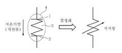
도 1a 및 도 1b는 종래의 상 변화 저항(PCR : Phase Change Resistor) 소자(4)를 설명하기 위한 도면이다.1A and 1B are diagrams for explaining a conventional phase change resistor (PCR)
상 변화 저항 소자(4)는 탑(Top) 전극(1)과 버텀(Bottom) 전극(3) 사이에 상 변화층(PCM; Phase Change Material;2)을 삽입하여 전압과 전류를 인가하면, 상 변화층(2)에 고온이 유기되어 저항에 변화에 따른 전기 전도 상태가 변하게 된다. 여기서, 상 변화층(2)의 재료로는 AglnSbTe가 주로 사용된다. 그리고, 상 변화층(2)은 칼코겐(chalcogen) 원소 (S, Se, Te)를 주성분으로 하는 화합 물(chalcogenide)을 이용하는데, 구체적으로 Ge-Sb-Te로 이루어진 게르마늄 안티몬 텔루르 합금물질(Ge2Sb2Te5)을 이용한다.When the phase
도 2a 및 도 2b는 종래의 상 변화 저항 소자의 원리를 설명하기 위한 도면이다.2A and 2B are diagrams for explaining the principle of a conventional phase change resistance element.
도 2a에서와 같이 상 변화 저항 소자(4)에 임계값 이하의 저전류가 흐르면 상 변화층(2)이 결정화가 되기에 적당한 온도가 된다. 이에 따라, 상 변화층(2)이 결정 상태(Crystalline phase)가 되어 저저항 상태의 물질이 된다.As shown in FIG. 2A, when a low current of less than or equal to a threshold flows through the phase
반면에, 도 2b에서와 같이 상 변화 저항 소자(4)에 임계값 이상의 고전류가 흐르면 상 변화층(2)이 녹는 점(Melting Point) 이상의 온도가 된다. 이에 따라, 상 변화층(2)이 비결정 상태가(Amorphous phase) 되어 고저항 상태의 물질이 된다.On the other hand, as shown in FIG. 2B, when a high current of more than a threshold flows through the phase
이와 같이 상 변화 저항 소자(4)는 두 저항의 상태에 대응하는 데이터를 불휘발성으로 저장할 수 있게 된다. 즉, 상 변화 저항 소자(4)가 저저항 상태일 경우를 데이터 "1"이라 하고, 고저항 상태일 경우를 데이터 "0"이라 하면 두 데이터의 로직 상태를 저장할 수 있다.As described above, the phase change
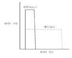
도 3은 종래의 상 변화 저항 셀의 라이트 동작을 설명하기 위한 도면이다.3 is a view for explaining a write operation of a conventional phase change resistance cell.
상 변화 저항 소자(4)의 탑 전극(1)과 버텀 전극(3) 사이에 일정 시간 동안 전류를 흘리게 되면 고 열이 발생하게 된다. 이에 따라, 탑 전극(1)과 버텀 전극(3)에 가해 준 온도 상태에 의해 상 변화층(2)의 상태가 결정상과 비결정상으로 변하게 된다.When a current flows between the
이때, 일정 시간 동안 저 전류를 흘리게 되면 저온 가열 상태에 의해 결정상 이 형성되어 저 저항 소자인 상 변화 저항 소자(4)가 세트(SET) 상태가 된다. 반대로, 일정 시간 동안 고 전류를 흘리게 되면 고온 가열 상태에 의해 비결정상이 형성되어 고 저항 소자인 상 변화 저항 소자(4)가 리셋(RESET) 상태가 된다. 따라서, 이 두 개의 상(Phase) 차이가 전기적인 저항 변화로 표현되어 나타나게 된다.At this time, when a low current flows for a predetermined time, a crystal phase is formed by a low temperature heating state, and the phase
이에 따라, 라이트 동작 모드시 세트(Set) 상태를 라이트 하기 위해 상 변화 저항 소자(4)에 낮은 전압을 긴 시간 동안 인가하게 된다. 반면에, 라이트 동작 모드시 리셋(Reset) 상태를 라이트 하기 위해 상 변화 저항 소자(4)에 높은 전압을 짧은 시간 동안 인가하게 된다.Accordingly, a low voltage is applied to the phase
하지만, 이러한 상 변화 저항 소자를 이용한 상 변화 메모리 장치의 가장 큰 문제점 중의 하나가 바로 셀에 데이터를 라이트 하기 위한 라이트 전류가 너무 크다는 것이다. 따라서, 데이터를 동시에 라이트할 수 있는 셀의 수가 제한적이어서 라이트 성능이 현격히 저하되는 단점이 있다.However, one of the biggest problems of the phase change memory device using the phase change resistance element is that the write current for writing data to the cell is too large. Therefore, the number of cells that can write data at the same time has a disadvantage in that the write performance is significantly reduced.
본 발명은 다음과 같은 목적을 갖는다.The present invention has the following object.
첫째, 상 변화 저항 소자를 이용한 메모리 장치에 있어서 라이트 전류의 증가 없이 복수개의 셀에 데이터를 동시에 라이트하고 라이트 시간을 줄일 수 있도록 하는데 그 목적이 있다.First, in a memory device using a phase change resistance element, the purpose of the present invention is to simultaneously write data to a plurality of cells and to reduce the write time without increasing the write current.
둘째, 수직 셀 구조의 상 변화 메모리 장치를 구현하여 셀 사이즈를 더욱 효과적으로 줄이고 라이트 특성을 개선할 수 있도록 하는데 그 목적이 있다.Second, the purpose of the present invention is to implement a phase change memory device having a vertical cell structure to more effectively reduce cell size and improve light characteristics.
셋째, 수직 셀 구조의 상 변화 메모리 장치를 다층으로 구현하여 셀 사이즈를 더욱 효과적으로 줄일 수 있도록 하는데 그 목적이 있다.Third, the purpose of the present invention is to implement a phase change memory device having a vertical cell structure in multiple layers so that the cell size can be more effectively reduced.
상기한 목적을 달성하기 위한 본 발명의 상 변화 메모리 장치는, 반도체 기판의 상부에 일정간격 이격 되어 형성되어 채널 영역과, 소스 및 드레인 영역을 포함하며 다층으로 적층된 복수개의 수직 채널 레이어; 복수개의 수직 채널 레이어의 하부에 형성된 소스 및 드레인 영역 중 인접한 소스 및 드레인 영역을 쌍으로 연결하도록 형성된 액티브 영역; 채널 영역의 양측에 형성된 게이트 산화막; 게이트 산화막에 접속하여 형성된 비트라인; 복수개의 수직 채널 레이어의 상부에 형성된 소스 및 드레인 영역 중 인접한 수직 채널 레이어의 소스 및 드레인 영역을 쌍으로 연결하여 전기적으로 접속시키는 도체 레이어; 도체 레이어의 전면에 형성되어 액티브 영역과 접속되는 수직 상 변화층; 및 수직 상 변화층의 상측에 형성된 워드라인을 포함하는 것을 특징으로 한다.According to an aspect of the present invention, there is provided a phase change memory device including: a plurality of vertical channel layers formed on a semiconductor substrate at regular intervals and including a channel region, a source and a drain region, and stacked in multiple layers; An active region formed to connect adjacent source and drain regions among pairs of source and drain regions formed under the plurality of vertical channel layers; Gate oxide films formed on both sides of the channel region; A bit line formed in connection with the gate oxide film; A conductor layer connecting and electrically connecting source and drain regions of adjacent vertical channel layers among the source and drain regions formed on the plurality of vertical channel layers in pairs; A vertical phase change layer formed on the front surface of the conductor layer and connected to the active region; And a word line formed on an upper side of the vertical phase change layer.
또한, 본 발명의 상 변화 메모리 장치의 형성 방법은, 반도체 기판상에 일정간격 이격되도록 액티브 영역을 형성하는 단계; 채널 영역과, 소스 및 드레인 영역을 포함하며 일정 간격 이격된 다수의 수직 채널 레이어를 상기 반도체 기판의 상부에 다층으로 적층하는 단계; 소스 및 드레인 영역을 패터닝하여 다수의 수직 채널 레이어를 분리하고, 다수의 수직 채널 레이어 중 인접한 수직 채널 레이어가 액티브 영역과 쌍으로 연결되도록 형성하는 단계; 채널 영역의 양측에 게이트 산화막을 형성하는 단계; 게이트 산화막과 접속되는 비트라인을 형성하는 단계; 다수의 수직 채널 레이어 사이에 절연층을 형성하는 단계; 다수의 수직 채널 레이어의 상부에 도체 레이어를 형성하여 인접한 수직 채널 레이어 상부에 형성된 소스 및 드레인 영역을 쌍으로 연결하여 전기적으로 접속시키는 단계; 액티브 영역이 노출되도록 절연층을 식각하여 트랜치 영역을 형성하는 단계; 도체 레이어의 상부 및 트랜치 영역의 전면에 수직 상 변화층을 형성하는 단계; 및 수직 상 변화층의 상측에 워드라인을 형성하는 단계를 포함하는 것을 특징으로 한다.In addition, the method of forming a phase change memory device of the present invention comprises the steps of: forming an active region on a semiconductor substrate at regular intervals; Stacking a plurality of vertical channel layers including a channel region, a source and a drain region, and spaced apart at regular intervals on the semiconductor substrate in multiple layers; Patterning the source and drain regions to separate a plurality of vertical channel layers, and forming adjacent pairs of vertical channel layers in pairs with the active regions; Forming gate oxide films on both sides of the channel region; Forming a bit line connected to the gate oxide film; Forming an insulating layer between the plurality of vertical channel layers; Forming a conductor layer on top of the plurality of vertical channel layers to electrically connect the source and drain regions formed on the adjacent vertical channel layer in pairs and electrically connect the pairs; Etching the insulating layer to expose the active region to form a trench region; Forming a vertical phase change layer on top of the conductor layer and in front of the trench region; And forming a word line on the upper side of the vertical phase change layer.
본 발명은 다음과 같은 효과를 제공한다.The present invention provides the following effects.
첫째, 상 변화 저항 소자를 이용한 메모리 장치에 있어서 라이트 전류의 증가 없이 복수개의 셀에 데이터를 동시에 라이트하고 라이트 시간을 줄일 수 있도록 한다.First, in a memory device using a phase change resistance device, data can be simultaneously written to a plurality of cells and the write time can be reduced without increasing the write current.
둘째, 수직 셀 구조의 상 변화 메모리 장치를 구현하여 셀 사이즈를 더욱 효과적으로 줄이고 라이트 특성을 개선할 수 있도록 한다.Second, by implementing a phase change memory device having a vertical cell structure, it is possible to more effectively reduce the cell size and improve the write characteristics.
셋째, 수직 셀 구조의 상 변화 메모리 장치를 다층으로 구현하여 칩 사이즈를 더욱 효과적으로 줄일 수 있도록 하는 효과를 제공한다.Third, the multi-phase phase change memory device having a vertical cell structure may be implemented in a multi-layer structure, thereby reducing chip size more effectively.
아울러 본 발명의 바람직한 실시예는 예시의 목적을 위한 것으로, 당업자라면 첨부된 특허청구범위의 기술적 사상과 범위를 통해 다양한 수정, 변경, 대체 및 부가가 가능할 것이며, 이러한 수정 변경 등은 이하의 특허청구범위에 속하는 것으로 보아야 할 것이다.It will be apparent to those skilled in the art that various modifications, additions, and substitutions are possible, and that various modifications, additions and substitutions are possible, within the spirit and scope of the appended claims. As shown in Fig.
이하, 첨부한 도면을 참조하여 본 발명의 실시예에 대해 상세히 설명하고자 한다.Hereinafter, embodiments of the present invention will be described in detail with reference to the accompanying drawings.
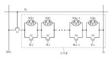
도 4a는 본 발명에 따른 상 변화 메모리 장치의 회로도이다.4A is a circuit diagram of a phase change memory device according to the present invention.
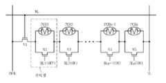
본 발명은 선택 스위치 N1와, 복수개의 상 변화 저항 셀 PCR1~PCRn 및 복수개의 스위칭 소자 N2~N5를 포함한다.The present invention includes a selection switch N1, a plurality of phase change resistance cells PCR1 to PCRn and a plurality of switching elements N2 to N5.
여기서, 선택 스위치 N1와 복수개의 스위칭 소자 N2~N5는 NMOS트랜지스터로 이루어지는 것이 바람직하다. 선택 스위치 N1는 리드/라이트 비트라인 RWBL과 단위 셀 UC1 사이에 연결되어 게이트 단자가 워드라인 WL과 연결된다.Here, it is preferable that the selection switch N1 and the plurality of switching elements N2 to N5 consist of NMOS transistors. The select switch N1 is connected between the read / write bitline RWBL and the unit cell UC1 so that the gate terminal is connected to the wordline WL.
그리고, 각각의 단위 셀 UC1은 하나의 상 변화 저항 셀 PCR1과 하나의 스위칭 소자 N2가 병렬로 연결된다. 상 변화 저항 셀 PCR1의 한쪽 전극은 스위칭 소자 N2의 소스 단자와 연결되고, 상 변화 저항 셀 PCR1의 다른 쪽 전극은 스위칭 소자 N2의 드레인 단자와 연결된다. 또한, 스위칭 소자 N2~N5의 게이트 단자는 복수개의 비트라인 BL1~BLn에 일대일 대응하여 연결된다.In each unit cell UC1, one phase change resistance cell PCR1 and one switching element N2 are connected in parallel. One electrode of the phase change resistance cell PCR1 is connected to the source terminal of the switching element N2, and the other electrode of the phase change resistance cell PCR1 is connected to the drain terminal of the switching element N2. In addition, the gate terminals of the switching elements N2 to N5 are connected one-to-one to the plurality of bit lines BL1 to BLn.
또한, 복수개의 상 변화 저항 셀 RCR1~RCRn 들은 선택 스위치 N1와 소스 라인 SL 사이에서 서로 직렬 연결된다. 즉, 한 개의 상 변화 저항 셀 PCR1의 소스 단자는 인접한 상 변화 저항 셀 PCR2의 드레인 단자에 연결된다. 직렬 연결된 복수개의 상 변화 저항 셀 RCR1~PCRn들 중 첫 번째 상 변화 저항 셀 PCR1은 선택 스위치 N1에 연결되고, 마지막 상 변화 저항 셀 PCRn은 소스라인 SL에 연결된다.In addition, the plurality of phase change resistance cells RCR1 to RCRn are connected in series with each other between the select switch N1 and the source line SL. That is, the source terminal of one phase change resistance cell PCR1 is connected to the drain terminal of the adjacent phase change resistance cell PCR2. The first phase change resistance cell PCR1 of the plurality of phase change resistance cells RCR1 to PCRn connected in series is connected to the selection switch N1, and the last phase change resistance cell PCRn is connected to the source line SL.
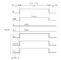
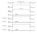
도 4b는 도 4a의 상 변화 메모리 장치에 관한 리드 모드시의 동작 파형도이다.4B is an operation waveform diagram in the read mode of the phase change memory device of FIG. 4A.
본 발명에서는 리드 모드시 상 변화 저항 셀 PCR1과 스위칭 소자 N2를 포함하는 첫 번째 단위 셀이 선택된 경우를 가정한다. 이러한 경우 선택된 셀과 연결되는 비트라인 BL1에 로우 전압이 인가되어 선택된 단위 셀은 오프 상태를 유지하게 된다. 그리고, 나머지 비선택된 셀과 연결된 비트라인 BL2~BLn 들에 하이 전압이 인가되어 비선택된 단위 셀 들은 모두 온 상태를 유지하게 된다.In the present invention, it is assumed that the first unit cell including the phase change resistance cell PCR1 and the switching element N2 is selected in the read mode. In this case, a low voltage is applied to the bit line BL1 connected to the selected cell to maintain the selected unit cell in an off state. In addition, a high voltage is applied to the bit lines BL2 to BLn connected to the remaining unselected cells so that all unselected unit cells remain on.
먼저, t0 구간에서는 워드라인 WL, 리드/라이트 비트라인 RWBL, 소스라인 SL 및 복수개의 비트라인 BL1~BLn 들은 모두 로우 레벨을 유지하게 된다. 이에 따라, 선택 스위치 N1가 턴오프 상태를 유지하게 되어 단위 셀과 리드/라이트 비트라인 RWBL 과의 연결이 차단된다.First, in the t0 period, the word line WL, the read / write bit line RWBL, the source line SL, and the plurality of bit lines BL1 to BLn all maintain the low level. As a result, the selection switch N1 is maintained in the turn-off state, thereby disconnecting the unit cell from the read / write bit line RWBL.
이후에, 리드 구간 t1의 진입시 워드라인 WL이 하이 레벨로 천이하게 된다. 이에 따라, 선택 스위치 N1가 턴온되어 선택된 단위 셀의 상 변화 저항 셀 PCR1이 리드/라이트 비트라인 RWBL과 연결된다.Subsequently, upon entering the read period t1, the word line WL transitions to a high level. Accordingly, the select switch N1 is turned on to connect the phase change resistance cell PCR1 of the selected unit cell with the read / write bit line RWBL.
이때, 소스 라인 SL은 그라운드 전압 레벨을 유지하게 된다. 그리고, 선택 셀과 연결된 비트라인 BL1에 그라운드 전압이 인가되어 스위칭 소자 N2가 턴오프 상태를 유지하게 된다.At this time, the source line SL maintains the ground voltage level. In addition, the ground voltage is applied to the bit line BL1 connected to the selection cell to maintain the switching element N2 in the turn-off state.
그리고, 비선택된 셀과 연결된 나머지 비트라인 BL2~BLn 들은 하이 전압 레벨로 천이하게 된다. 이에 따라, 나머지 비트라인 BL2~BLn 들과 연결된 스위칭 소자 N3~N5는 모두 턴온되어, 상 변화 저항 셀 PCR1과 소스 라인 SL 사이에서 직렬 연결된 상태가 된다.Then, the remaining bit lines BL2 to BLn connected to the unselected cell transition to the high voltage level. As a result, all of the switching elements N3 to N5 connected to the remaining bit lines BL2 to BLn are turned on to be in series connection between the phase change resistance cell PCR1 and the source line SL.
또한, 리드/라이트 비트라인 RWBL에 셀 구동 전압 중 데이터를 센싱하기 위한 센싱 전압 Vsense을 인가한다. 이에 따라, 선택된 단위 셀에 해당하는 상 변화 저항 셀 PCR1에서 리드된 전류가 리드/라이트 비트라인 RWBL과 소스 라인 SL 사이에 흐르게 된다.In addition, a sensing voltage Vsense for sensing data among cell driving voltages is applied to the read / write bit line RWBL. Accordingly, the current read in the phase change resistance cell PCR1 corresponding to the selected unit cell flows between the read / write bit line RWBL and the source line SL.
도 5a 및 도 5b는 본 발명에 따른 상 변화 메모리 장치의 회로도 및 라이트 모드시의 동작 파형도이다.5A and 5B are circuit diagrams of the phase change memory device according to the present invention and operational waveform diagrams in the write mode.
본 발명에서는 라이트 모드시 선택 스위치 N1과 소스 라인 SL 사이에 연결된 모든 단위 셀이 선택된 경우를 가정한다. 이러한 경우 모든 단위 셀과 연결되는 비트라인 BL1~BLn 들에 인가되는 전압을 선택적으로 조정하여 해당 데이터를 복수개의 상 변화 저항 셀 PCR1~PCRn에 동시에 라이트 하게 된다.In the present invention, it is assumed that all unit cells connected between the selection switch N1 and the source line SL are selected in the write mode. In this case, the voltages applied to the bit lines BL1 to BLn connected to all the unit cells are selectively adjusted to simultaneously write the corresponding data to the plurality of phase change resistance cells PCR1 to PCRn.
먼저, t0 구간에서는 워드라인 WL, 리드/라이트 비트라인 RWBL, 소스라인 SL 및 복수개의 비트라인 BL1~BLn 들은 모두 로우 레벨을 유지하게 된다. 이에 따라, 선택 스위치 N1가 턴오프 상태를 유지하게 되어 단위 셀과 리드/라이트 비트라인 RWBL 과의 연결이 차단된다.First, in the t0 period, the word line WL, the read / write bit line RWBL, the source line SL, and the plurality of bit lines BL1 to BLn all maintain the low level. As a result, the selection switch N1 is maintained in the turn-off state, thereby disconnecting the unit cell from the read / write bit line RWBL.
이후에, 라이트 구간 t1의 진입시 워드라인 WL이 하이 레벨로 천이하게 된다. 이에 따라, 선택 스위치 N1가 턴온되어 모든 단위 셀 중 상 변화 저항 셀 PCR1이 리드/라이트 비트라인 RWBL과 연결된다.Thereafter, the word line WL transitions to a high level when the write period t1 is entered. Accordingly, the select switch N1 is turned on so that the phase change resistance cell PCR1 of all the unit cells is connected to the read / write bit line RWBL.
이때, 소스 라인 SL은 그라운드 전압 레벨을 유지하게 된다. 그리고, 리드/라이트 비트라인 RWBL에 셀 구동 전압 중 데이터를 라이트 하기 위한 라이트 전압 Vwrite을 인가한다. 이에 따라, 모든 상 변화 저항 셀 PCR1~PCRn에 해당하는 데이터를 각각 동시에 라이트 할 수 있게 된다.At this time, the source line SL maintains the ground voltage level. The write voltage Vwrite for writing data among the cell driving voltages is applied to the read / write bit line RWBL. As a result, data corresponding to all the phase change resistance cells PCR1 to PCRn can be written at the same time.
예를 들어, 상 변화 저항 셀 PCR1에 세트(Set) 상태, 즉, 데이터 "0"을 라이트 할 경우, 상 변화 저항 셀 PCR1과 연결된 비트라인 BL1이 하이 전압 레벨로 천이하게 된다. 이에 따라, 스위칭 소자 N2가 턴온 되어 선택 스위치 N1를 통해 인가되는 라이트 전압 Vwrite이 상 변화 저항 셀 PCR1과 스위칭 소자 N2에 인가된다.For example, when the set state, that is, data "0", is written to the phase change resistance cell PCR1, the bit line BL1 connected to the phase change resistance cell PCR1 transitions to a high voltage level. Thus, the switching element N2 is turned on and the write voltage Vwrite applied through the selection switch N1 is applied to the phase change resistance cell PCR1 and the switching element N2.
따라서, 라이트 전류가 상 변화 저항 셀 PCR1과 스위칭 소자 N2에 나누어 흐르게 된다. 이러한 경우 상 변화 저항 셀 PCR1에 흐르는 전류는 전체 전류에 비해 작아지게 되어 상 변화 저항 셀 PCR1에 데이터 "0"이 라이트 된다. 즉, 선택 스위치 N1에 흐르는 전체 전류를 리셋 전류(Reset current)로 가정할 경우, 상 변화 저항 셀 PCR1에 리셋 전류보다 낮은 세트 전류(Set current)가 흐르게 된다.Therefore, the write current flows into the phase change resistance cell PCR1 and the switching element N2. In this case, the current flowing through the phase change resistance cell PCR1 becomes smaller than the total current, and data "0" is written to the phase change resistance cell PCR1. That is, assuming that the total current flowing through the select switch N1 is a reset current, a set current lower than the reset current flows through the phase change resistance cell PCR1.
그리고, 상 변화 저항 셀 PCR2에 리셋(Reset) 상태, 즉, 데이터 "1"을 라이트 할 경우, 상 변화 저항 셀 PCR2과 연결된 비트라인 BL2이 로우 전압 레벨을 유지하게 된다. 이에 따라, 스위칭 소자 N3가 턴오프 되어 선택 스위치 N1를 통해 인가되는 라이트 전압 Vwrite이 상 변화 저항 셀 PCR2과 스위칭 소자 N3에 인가된다.When the reset state, that is, data "1", is written to the phase change resistance cell PCR2, the bit line BL2 connected to the phase change resistance cell PCR2 maintains the low voltage level. Accordingly, the switching element N3 is turned off and the write voltage Vwrite applied through the selection switch N1 is applied to the phase change resistance cell PCR2 and the switching element N3.
따라서, 라이트 전류가 상 변화 저항 셀 PCR2에만 흐르게 된다. 이러한 경 우 상 변화 저항 셀 PCR2에 흐르는 전류는 전체 전류에 해당하게 되어 상 변화 저항 셀 PCR2에 데이터 "1"이 라이트 된다. 즉, 선택 스위치 N1에 흐르는 전체 전류를 리셋 전류(Reset current)로 가정할 경우, 상 변화 저항 셀 PCR2에 리셋 전류가 흐르게 된다.Therefore, the write current flows only in the phase change resistance cell PCR2. In this case, the current flowing through the phase change resistance cell PCR2 corresponds to the total current, and data "1" is written to the phase change resistance cell PCR2. That is, assuming that the entire current flowing through the selector switch N1 is a reset current, the reset current flows through the phase change resistance cell PCR2.
또한, 상 변화 저항 셀 PCRn-1에 세트(Set) 상태, 즉, 데이터 "0"을 라이트 할 경우, 상 변화 저항 셀 PCRn-1과 연결된 비트라인 BLn-1이 하이 전압 레벨로 천이하게 된다. 이에 따라, 스위칭 소자 N4가 턴온 되어 선택 스위치 N1를 통해 인가되는 라이트 전압 Vwrite이 상 변화 저항 셀 PCRn-1과 스위칭 소자 N4에 인가된다.When the set state, that is, data "0", is written to the phase change resistance cell PCRn-1, the bit line BLn-1 connected to the phase change resistance cell PCRn-1 transitions to a high voltage level. Thus, the switching element N4 is turned on and the write voltage Vwrite applied through the selection switch N1 is applied to the phase change resistance cell PCRn-1 and the switching element N4.
따라서, 라이트 전류가 상 변화 저항 셀 PCRn-1과 스위칭 소자 N4에 나누어 흐르게 된다. 이러한 경우 상 변화 저항 셀 PCRn-1에 흐르는 전류는 전체 전류에 비해 작아지게 되어 상 변화 저항 셀 PCRn-1에 데이터 "0"이 라이트 된다. 즉, 선택 스위치 N1에 흐르는 전체 전류를 리셋 전류(Reset current)로 가정할 경우, 상 변화 저항 셀 PCRn-1에 리셋 전류보다 낮은 세트 전류(Set current)가 흐르게 된다.Therefore, the write current flows into the phase change resistance cell PCRn-1 and the switching element N4. In this case, the current flowing in the phase change resistance cell PCRn-1 becomes smaller than the total current, and data "0" is written in the phase change resistance cell PCRn-1. That is, assuming that the total current flowing through the selection switch N1 is a reset current, a set current lower than the reset current flows through the phase change resistance cell PCRn-1.
그리고, 상 변화 저항 셀 PCRn에 리셋(Reset) 상태, 즉, 데이터 "1"을 라이트 할 경우, 상 변화 저항 셀 PCRn과 연결된 비트라인 BLn이 로우 전압 레벨을 유지하게 된다. 이에 따라, 스위칭 소자 N5가 턴오프 되어 선택 스위치 N1를 통해 인가되는 라이트 전압 Vwrite이 상 변화 저항 셀 PCRn과 스위칭 소자 N5에 인가된다.When the reset state, that is, data "1", is written to the phase change resistance cell PCRn, the bit line BLn connected to the phase change resistance cell PCRn maintains the low voltage level. As a result, the switching element N5 is turned off and the write voltage Vwrite applied through the selection switch N1 is applied to the phase change resistance cell PCRn and the switching element N5.
따라서, 라이트 전류가 상 변화 저항 셀 PCRn에만 흐르게 된다. 이러한 경우 상 변화 저항 셀 PCRn에 흐르는 전류는 전체 전류에 해당하게 되어 상 변화 저항 셀 PCRn에 데이터 "1"이 라이트 된다. 즉, 선택 스위치 N1에 흐르는 전체 전류를 리셋 전류(Reset current)로 가정할 경우, 상 변화 저항 셀 PCRn에 리셋 전류가 흐르게 된다.Therefore, the write current flows only in the phase change resistance cell PCRn. In this case, the current flowing through the phase change resistance cell PCRn corresponds to the total current, and data "1" is written to the phase change resistance cell PCRn. That is, assuming that the total current flowing through the selection switch N1 is a reset current, the reset current flows through the phase change resistance cell PCRn.
이와 같이, 선택 스위치 N1를 통해 흐르게 되는 전체 전류는 동일하고, 세트 상태가 라이트 되는 상 변화 저항 셀 PCR1,PCRn-1에는 작은 세트 전류가 흐르게 되며, 리셋 상태가 라이트 되는 상 변화 저항 셀 PCR2,PCRn에는 큰 리셋 전류가 흐르게 된다.In this way, the total current flowing through the selector switch N1 is the same, and a small set current flows in the phase change resistance cells PCR1 and PCRn-1 in which the set state is written, and the phase change resistance cells PCR2 and PCRn in which the reset state is written. Large reset current flows through it.
이러한 본 발명은 직렬 연결된 상 변화 저항 셀 PCR1~PCRn에 따라, 라이트 전류의 증가 없이 복수개의 상 변화 저항 셀 PCR1~PCRn에 동시에 데이터를 라이트할 수 있도록 한다. 이에 따라, 본 발명은 종래 기술에 비해 셀에 데이터를 라이트 하기 위한 라이트 전류의 크기를 1/N로 줄일 수 있게 된다. 그리고, 본 발명은 종래 기술에 비해 셀에 데이터를 라이트 하기 위한 라이트 시간을 1/N로 줄일 수 있게 된다.According to the present invention, data can be simultaneously written to a plurality of phase change resistance cells PCR1 to PCRn without increasing the write current according to the series-connected phase change resistance cells PCR1 to PCRn. Accordingly, the present invention can reduce the size of the write current for writing data to the cell to 1 / N, compared with the prior art. According to the present invention, the write time for writing data into a cell can be reduced to 1 / N, compared with the related art.
도 6은 본 발명에 따른 상 변화 메모리 장치의 셀 어레이를 나타낸 도면이다.6 illustrates a cell array of a phase change memory device according to the present invention.
본 발명은 복수개의 리드/라이트 비트라인 RWBL1~RWBLn이 로오 방향으로 배열된다. 그리고, 복수개의 비트라인 BL1~BLn이 로오 방향으로 배열된다. 또한, 복수개의 워드라인 WL1~WLn이 컬럼 방향으로 배열된다.In the present invention, a plurality of read / write bit lines RWBL1 to RWBLn are arranged in the row direction. The plurality of bit lines BL1 to BLn are arranged in the row direction. Further, a plurality of word lines WL1 to WLn are arranged in the column direction.
또한, 복수개의 리드/라이트 비트라인 RWBL1~RWBLn과 복수개의 워드라인 WL1~WLn이 교차하는 영역에 선택 스위치 N1가 배열된다. 이러한 선택 스위치 N1는 로오 및 컬럼 방향으로 복수개 배열된다.Further, the selection switch N1 is arranged in an area where the plurality of read / write bit lines RWBL1 to RWBLn and the plurality of word lines WL1 to WLn intersect. A plurality of such selection switches N1 are arranged in the row and column directions.
그리고, 복수개의 비트라인 BL1~BLn과 복수개의 워드라인 WL1~WLn이 교차하는 영역에 단위 셀 UC이 배열된다. 이러한 단위 셀 UC은 로오 및 컬럼 방향으로 복수개 배열된다. 여기서, 하나의 리드/라이트 비트라인 RWBL은 복수개의 선택 스위치 N1에 의해 공유된다. 그리고, 하나의 소스 라인 SL은 복수개의 단위 셀 UC에 의해 공유된다.The unit cell UC is arranged in an area where the plurality of bit lines BL1 to BLn and the plurality of word lines WL1 to WLn intersect. A plurality of such unit cells UC are arranged in the row and column directions. Here, one read / write bitline RWBL is shared by the plurality of select switches N1. One source line SL is shared by a plurality of unit cells UC.
또한, 리드/라이트 비트라인 RWBL은 센스앰프 SA 및 글로벌 라이트 구동부 GWD에 연결된다. 이에 따라, 센스앰프 SA는 리드 동작 모드시 리드/라이트 비트라인 RWBL을 통해 인가되는 센싱 전압 Vsense을 센싱 및 증폭하게 된다. 그리고, 글로벌 라이트 구동부 GWD는 라이트 동작 모드시 리드/라이트 비트라인 RWBL에 라이트 전압 Vwrite을 공급하게 된다.In addition, the read / write bit line RWBL is connected to the sense amplifier SA and the global write driver GWD. Accordingly, the sense amplifier SA senses and amplifies the sensing voltage Vsense applied through the read / write bit line RWBL in the read operation mode. The global write driver GWD supplies the write voltage Vwrite to the read / write bit line RWBL in the write operation mode.
그리고, 각각의 비트라인 BL은 라이트 구동부 WD에 연결된다. 이에 따라, 리드 또는 라이트 동작 모드시 라이트 구동부 WD의 전압에 따라 비트라인 BL에 인가되는 전압을 선택적으로 제어하여 해당하는 단위 셀 UC을 선택하도록 한다.Each bit line BL is connected to the write driver WD. Accordingly, the voltage applied to the bit line BL is selectively controlled according to the voltage of the write driver WD in the read or write operation mode to select the corresponding unit cell UC.
또한, 소스 라인 SL은 소스 구동부 SD에 연결된다. 이에 따라, 리드 또는 라이트 동작 모드시 소스 구동부 SD의 전압(그라운드 전압)에 따라 소스 라인 SL에 인가되는 전압을 선택적으로 조정할 수 있도록 한다.In addition, the source line SL is connected to the source driver SD. Accordingly, the voltage applied to the source line SL may be selectively adjusted according to the voltage (ground voltage) of the source driver SD in the read or write operation mode.
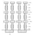
도 7 내지 도 23은 본 발명에 따른 상 변화 메모리 장치의 형성 방법을 나타 낸 단면도이다.7 to 23 are cross-sectional views illustrating a method of forming a phase change memory device according to the present invention.
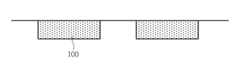
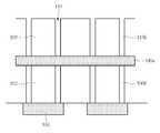
먼저, 도 7에서와 같이, 직렬 셀을 서로 연결하기 위한 N+ 액티브 영역(100)을 반도체 기판상에 일정간격 이격 되도록 형성한다.First, as illustrated in FIG. 7, N +
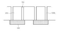
이후에, 도 8에서와 같이, 반도체 기판의 상부에 첫 번째 산화막(102)을 증착한다. 그리고, 산화막(102)을 식각하여 수직 채널 레이어를 형성하기 위한 홀(Hole;104)을 형성한다.Thereafter, as shown in FIG. 8, the
이때, 홀(104)은 반도체 기판상에 형성된 N+ 액티브 영역(100)이 노출되는 깊이까지 형성하게 된다. 그리고, 하나의 N+ 액티브 영역(100)이 적어도 2개의 홀(104)과 연결되도록 형성한다.In this case, the
다음에, 도 9에서와 같이, 첫 번째 반도체 영역을 성장시켜 채널 영역(106b)과, 소스 및 드레인 영역(106a)을 포함하는 수직 채널 레이어(Vertical channel layer)를 형성한다. 여기서, 수직 채널 레이어의 채널 영역(106b)은 일정 간격 이격되어 복수개 형성된다. 그리고, 반도체 영역을 성장시킬 경우 홀(104)에 수직 채널 레이어의 채널 영역(106b)이 채워지게 된다.Next, as shown in FIG. 9, the first semiconductor region is grown to form a vertical channel layer including the
본 발명의 실시예에서는 수직 채널 레이어의 형성시 반도체 영역을 성장시키는 것을 그 실시예로 설명하였다. 하지만, 본 발명은 이에 한정되는 것이 아니며, 반도체 웨이퍼를 식각하여 수직 채널 레이어를 형성할 수도 있다.In the embodiment of the present invention, the growth of the semiconductor region when the vertical channel layer is formed is described as the embodiment. However, the present invention is not limited thereto, and the semiconductor wafer may be etched to form a vertical channel layer.
다음에, 도 10에서와 같이, 수직 채널 레이어의 소스 및 드레인 영역(106a)에 N+의 고농도 불순물을 도핑 한다.Next, as shown in FIG. 10, the high concentration impurities of N + are doped into the source and
이후에, 도 11에서와 같이, 소스 및 드레인 영역(106a)의 상부에 두 번째 산 화막(108)을 증착한다. 그리고, 산화막(108)을 식각하여 수직 채널 레이어를 형성하기 위한 홀(110)을 형성한다.Thereafter, as shown in FIG. 11, a
이때, 홀(110)은 첫 번째 레이어의 소스 및 드레인 영역(106a)이 노출되는 깊이까지 형성하게 된다. 그리고, 각각의 홀(110)은 채널 영역(106b)의 상측에 위치하도록 형성된다.In this case, the
다음에, 도 12에서와 같이, 두 번째 반도체 영역을 성장시켜 채널 영역(112b)과, 소스 및 드레인 영역(112a)을 포함하는 수직 채널 레이어(Vertical channel layer)를 형성한다. 여기서, 수직 채널 레이어의 채널 영역(112b)은 일정 간격 이격되어 복수개 형성된다. 그리고, 반도체 영역을 성장시킬 경우 홀(110)에 수직 채널 레이어의 채널 영역(112b)이 채워지게 된다.Next, as shown in FIG. 12, the second semiconductor region is grown to form a vertical channel layer including the
이후에, 도 13에서와 같이, 수직 채널 레이어의 소스 및 드레인 영역(112a)에 N+의 고농도 불순물을 도핑 한다.Thereafter, as shown in FIG. 13, a high concentration of impurities of N + are doped into the source and
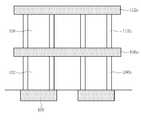
이어서, 도 14에서와 같이, 소스 및 드레인 영역(112a)의 상부에 세 번째 산화막(114)을 증착한다. 그리고, 산화막(114)을 식각하여 수직 채널 레이어를 형성하기 위한 홀(116)을 형성한다.Next, as shown in FIG. 14, a
이때, 홀(116)은 두 번째 레이어의 소스 및 드레인 영역(112a)이 노출되는 깊이까지 형성하게 된다. 그리고, 각각의 홀(116)은 채널 영역(112b)의 상측에 위치하도록 형성된다.In this case, the
다음에, 도 15에서와 같이, 세 번째 반도체 영역을 성장시켜 채널 영역(118b)과, 소스 및 드레인 영역(118a)을 포함하는 수직 채널 레이어(Vertical channel layer)를 형성한다. 여기서, 수직 채널 레이어의 채널 영역(118b)은 일정 간격 이격되어 복수개 형성된다. 그리고, 반도체 영역을 성장시킬 경우 홀(116)에 수직 채널 레이어의 채널 영역(118b)이 채워지게 된다.Next, as shown in FIG. 15, the third semiconductor region is grown to form a vertical channel layer including the
이후에, 도 16에서와 같이, 수직 채널 레이어의 소스 및 드레인 영역(118a)에 N+의 고농도 불순물을 도핑 한다.Thereafter, as shown in FIG. 16, the high concentration impurities of N + are doped into the source and
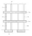
이어서, 도 17에서와 같이, N+ 불순물 영역이 도핑된 소스 및 드레인 영역(106a,112a,118a)을 식각하여 소스 및 드레인 영역의 패턴을 형성한다. 그리고, 수직 채널 레이어 상에 형성된 산화막(102,108,114)을 제거한다.17, the source and
각 셀의 소스 및 드레인 영역(106a,112a,118a)이 분리되어 형성됨으로써 각각의 수직 채널 레이어가 서로 분리될 수 있도록 한다. 이때, 인접한 수직 채널 레이어들은 그 하부에 형성된 N+ 액티브 영역(100)에 의해 소스 및 드레인 영역(106a,112a,118a)이 서로 연결될 수 있도록 한다. 여기서, 인접한 영역에 형성된 수직 채널 레이어들은 N+ 액티브 영역(100)에 의해 쌍으로 연결되는 것이 바람직하다.The source and
다음에, 도 18에서와 같이, 수직 채널 레이어에서 채널 영역(106b,112b,118b)의 양측 영역에 게이트 산화막(Gate Oxide Layer; 120a~120c)을 형성한다.Next, as illustrated in FIG. 18,
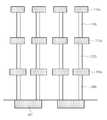
이후에, 도 19에서와 같이, 수직 게이트 라인인 비트라인(122a~122c)을 게이트 산화막(120a~120c)의 일부 영역에 형성한다. 이때, 수직 채널 레이어의 채널 영역(106b,112b,118b)이 소스 및 드레인 영역(106a,112a,118a) 보다 얇은 두께로 형성된다. 그리고, 채널 영역(106b,112b,118b)이 오목한 형태로 되어 있어 채널 영역(106b,112b,118b) 상에서 비트라인(122a~122c)이 두껍게 형성된다.Thereafter, as shown in FIG. 19,
이에 따라, 자체적으로 게이트 영역에만 비트라인(122a~122c)이 남게 되고, 소스 및 드레인 영역(106a,112a,118a)에 형성된 게이트 막은 먼저 식각 되어 없어지게 된다. 여기서, 비트라인(122a~122c)은 게이트 산화막(120a~120c)의 길이보다 더 짧은 길이를 갖도록 형성된다.As a result, the
이어서, 도 20에서와 같이, 수직 반도체 영역의 빈 공간에 절연물질을 채워 절연층(124)을 형성한다. 그리고, 직렬 셀을 구성하기 위해 수직 채널 레이어와, 게이트 산화막(120a~120c)과, 비트라인(122a~122c) 및 소스 및 드레인 영역(106a,112a,118a)을 포함하는 절연층(124)의 상부에 도체 레이어(126)를 형성한다.Next, as shown in FIG. 20, the insulating
이때, 도체 레이어(126)는 인접한 영역에 형성된 수직 셀 들의 소스 및 드레인 영역(106a,112a,118a)을 상호 전기적으로 연결되도록 한다. 이때, 도체 레이어(126)는 인접한 영역에 형성된 수직 채널 레이어를 쌍으로 연결하도록 형성되는 것이 바람직하다.In this case, the
이러한 도체 레이어(126)는 소스 및 드레인 영역(118a)이 형성된 상부 영역에 형성되며, N+ 액티브 영역(100)이 위치한 영역을 제외하고 절연층(124)과 접속되도록 형성된다.The
이후에, 도 21에서와 같이, 수직 상 변화층(PCM; Phase Change Material)을 형성하기 위해 절연층(124)의 일부를 식각하여 트랜치(Trench) 영역(128)을 형성한 다.Afterwards, as shown in FIG. 21, a portion of the insulating
이때, 트랜치 영역(128)은 절연층(124)의 내측에 형성된 게이트 산화막(120a~120c)과, 비트라인(122a~122c)이 노출되지 않도록 형성된다. 이에 따라, 식각된 절연층(124)은 스페이서(Spacer) 형태로 수직 채널 레이어의 측벽에 형성된다.In this case, the
그리고, 트랜치 영역(128)은 하부 영역으로 갈수록 그 폭이 좁아지도록 "V"자 형태로 형성된다. 또한, 트랜치 영역(128)은 최하부 영역에서 N+ 액티브 영역(100)이 노출되는 깊이까지 형성된다.The
이후에, 도 22에서와 같이, 트랜치 영역(128)과 도체 레이어(126)의 상부에 일정 두께를 갖는 수직 상 변화층(130)을 형성한다. 이때, 수직 상 변화층(130)은 N+ 액티브 영역(100)과 접속되도록 형성된다.Thereafter, as shown in FIG. 22, a vertical
여기서, 수직 상 변화층(130)의 재료로는 AglnSbTe가 주로 사용된다. 그리고, 상 변화층(130)은 칼코겐(chalcogen) 원소 (S, Se, Te)를 주성분으로 하는 화합물(chalcogenide)을 이용하는데, 구체적으로 Ge-Sb-Te로 이루어진 게르마늄 안티몬 텔루르 합금물질(Ge2Sb2Te5)을 이용한다.Here, AglnSbTe is mainly used as a material of the vertical
이어서, 도 23에서와 같이, 수직 상 변화층(130)의 상부 전면에 절연층(132)을 형성하고, 절연층(132)의 상부에 워드라인(134)을 형성한다.Next, as shown in FIG. 23, an insulating
도 1a 및 도 1b는 종래의 상 변화 저항 소자를 설명하기 위한 도면.1A and 1B are diagrams for explaining a conventional phase change resistance element.
도 2a 및 도 2b는 종래의 상 변화 저항 소자의 원리를 설명하기 위한 도면.2A and 2B are diagrams for explaining the principle of a conventional phase change resistance element.
도 3은 종래의 상 변화 저항 셀의 라이트 동작을 설명하기 위한 도면.3 is a view for explaining a write operation of a conventional phase change resistance cell.
도 4a 및 도 4b는 본 발명에 따른 상 변화 메모리 장치의 회로도 및 리드 모드시의 동작 파형도.4A and 4B are a circuit diagram of a phase change memory device according to the present invention and an operation waveform diagram in read mode.
도 5a 및 도 5b는 본 발명에 따른 상 변화 메모리 장치의 회로도 및 라이트 모드시의 동작 파형도.5A and 5B are a circuit diagram of a phase change memory device according to the present invention and an operation waveform diagram in write mode.
도 6은 본 발명에 따른 상 변화 메모리 장치의 셀 어레이를 나타낸 도면.6 illustrates a cell array of a phase change memory device according to the present invention.
도 7 내지 도 23은 본 발명에 따른 상 변화 메모리 장치의 형성 방법을 나타낸 평면도 및 단면도.7 to 23 are plan and cross-sectional views illustrating a method of forming a phase change memory device according to the present invention.
Claims (24)
Translated fromKoreanPriority Applications (1)
| Application Number | Priority Date | Filing Date | Title |
|---|---|---|---|
| KR1020080036125AKR100960462B1 (en) | 2008-04-18 | 2008-04-18 | Phase change memory device and forming method thereof |
Applications Claiming Priority (1)
| Application Number | Priority Date | Filing Date | Title |
|---|---|---|---|
| KR1020080036125AKR100960462B1 (en) | 2008-04-18 | 2008-04-18 | Phase change memory device and forming method thereof |
Publications (2)
| Publication Number | Publication Date |
|---|---|
| KR20090110557A KR20090110557A (en) | 2009-10-22 |
| KR100960462B1true KR100960462B1 (en) | 2010-05-31 |
Family
ID=41538393
Family Applications (1)
| Application Number | Title | Priority Date | Filing Date |
|---|---|---|---|
| KR1020080036125AExpired - Fee RelatedKR100960462B1 (en) | 2008-04-18 | 2008-04-18 | Phase change memory device and forming method thereof |
Country Status (1)
| Country | Link |
|---|---|
| KR (1) | KR100960462B1 (en) |
Cited By (1)
| Publication number | Priority date | Publication date | Assignee | Title |
|---|---|---|---|---|
| TWI697105B (en)* | 2018-12-21 | 2020-06-21 | 大陸商芯恩(青島)積體電路有限公司 | 3-dimensional junction semiconductor memory device and fabrication method thereof |
Citations (3)
| Publication number | Priority date | Publication date | Assignee | Title |
|---|---|---|---|---|
| JP2003229537A (en) | 2002-02-01 | 2003-08-15 | Hitachi Ltd | Semiconductor storage device and method of manufacturing the same |
| KR20050091902A (en)* | 2004-03-12 | 2005-09-15 | 가부시키가이샤 히타치세이사쿠쇼 | Semiconductor device |
| KR20090011452A (en)* | 2007-07-26 | 2009-02-02 | 삼성전자주식회사 | NAND-type resistive memory cell strings of a nonvolatile memory device and manufacturing methods thereof |
- 2008
- 2008-04-18KRKR1020080036125Apatent/KR100960462B1/ennot_activeExpired - Fee Related
Patent Citations (3)
| Publication number | Priority date | Publication date | Assignee | Title |
|---|---|---|---|---|
| JP2003229537A (en) | 2002-02-01 | 2003-08-15 | Hitachi Ltd | Semiconductor storage device and method of manufacturing the same |
| KR20050091902A (en)* | 2004-03-12 | 2005-09-15 | 가부시키가이샤 히타치세이사쿠쇼 | Semiconductor device |
| KR20090011452A (en)* | 2007-07-26 | 2009-02-02 | 삼성전자주식회사 | NAND-type resistive memory cell strings of a nonvolatile memory device and manufacturing methods thereof |
Cited By (1)
| Publication number | Priority date | Publication date | Assignee | Title |
|---|---|---|---|---|
| TWI697105B (en)* | 2018-12-21 | 2020-06-21 | 大陸商芯恩(青島)積體電路有限公司 | 3-dimensional junction semiconductor memory device and fabrication method thereof |
Also Published As
| Publication number | Publication date |
|---|---|
| KR20090110557A (en) | 2009-10-22 |
Similar Documents
| Publication | Publication Date | Title |
|---|---|---|
| JP5462490B2 (en) | Semiconductor memory device | |
| US9455301B2 (en) | Setting channel voltages of adjustable resistance bit line structures using dummy word lines | |
| JP5396544B2 (en) | Semiconductor memory device | |
| JP5512700B2 (en) | Semiconductor memory device and manufacturing method thereof | |
| CN109427969B (en) | Phase change memory electrodes with multiple thermal interfaces | |
| TWI424553B (en) | Circuit, biasing scheme and fabrication method for diode accessed cross-point resistive memory array | |
| US10355129B2 (en) | Vertical transistors with sidewall gate air gaps and methods therefor | |
| KR20180005778A (en) | Three-Dimensional Semiconductor Memory Device | |
| WO2011056474A1 (en) | Non-volatile memory array architecture incorporating 1t-1r near 4f2 memory cell | |
| KR101144443B1 (en) | Non-volatile memory including multi-layer memory cells and the manufacturing method thereof | |
| US7977661B2 (en) | Memory having shared storage material | |
| US9013917B2 (en) | Semiconductor memory device | |
| KR102611899B1 (en) | Non-volatile memory cell having embedded select device and memory cell array with the non-volatile memory cell | |
| CN108431978A (en) | Monolithic 3D memory array formed using sacrificial polysilicon pillars | |
| KR100929628B1 (en) | Phase change memory element | |
| KR100960462B1 (en) | Phase change memory device and forming method thereof | |
| KR100960461B1 (en) | Phase change memory device and forming method thereof | |
| KR100681810B1 (en) | Phase change memory cell array with high integration and high current driving force and high speed low power phase change memory semiconductor device | |
| KR20110001716A (en) | Phase change memory device | |
| CN120530726A (en) | Memory device having three-dimensional vertical structure and driving method thereof |
Legal Events
| Date | Code | Title | Description |
|---|---|---|---|
| A201 | Request for examination | ||
| PA0109 | Patent application | St.27 status event code:A-0-1-A10-A12-nap-PA0109 | |
| PA0201 | Request for examination | St.27 status event code:A-1-2-D10-D11-exm-PA0201 | |
| PG1501 | Laying open of application | St.27 status event code:A-1-1-Q10-Q12-nap-PG1501 | |
| D13-X000 | Search requested | St.27 status event code:A-1-2-D10-D13-srh-X000 | |
| D14-X000 | Search report completed | St.27 status event code:A-1-2-D10-D14-srh-X000 | |
| E902 | Notification of reason for refusal | ||
| PE0902 | Notice of grounds for rejection | St.27 status event code:A-1-2-D10-D21-exm-PE0902 | |
| E13-X000 | Pre-grant limitation requested | St.27 status event code:A-2-3-E10-E13-lim-X000 | |
| P11-X000 | Amendment of application requested | St.27 status event code:A-2-2-P10-P11-nap-X000 | |
| P13-X000 | Application amended | St.27 status event code:A-2-2-P10-P13-nap-X000 | |
| E701 | Decision to grant or registration of patent right | ||
| PE0701 | Decision of registration | St.27 status event code:A-1-2-D10-D22-exm-PE0701 | |
| GRNT | Written decision to grant | ||
| PR0701 | Registration of establishment | St.27 status event code:A-2-4-F10-F11-exm-PR0701 | |
| PR1002 | Payment of registration fee | St.27 status event code:A-2-2-U10-U11-oth-PR1002 Fee payment year number:1 | |
| PG1601 | Publication of registration | St.27 status event code:A-4-4-Q10-Q13-nap-PG1601 | |
| PN2301 | Change of applicant | St.27 status event code:A-5-5-R10-R13-asn-PN2301 St.27 status event code:A-5-5-R10-R11-asn-PN2301 | |
| PN2301 | Change of applicant | St.27 status event code:A-5-5-R10-R13-asn-PN2301 St.27 status event code:A-5-5-R10-R11-asn-PN2301 | |
| LAPS | Lapse due to unpaid annual fee | ||
| PC1903 | Unpaid annual fee | St.27 status event code:A-4-4-U10-U13-oth-PC1903 Not in force date:20130521 Payment event data comment text:Termination Category : DEFAULT_OF_REGISTRATION_FEE | |
| PC1903 | Unpaid annual fee | St.27 status event code:N-4-6-H10-H13-oth-PC1903 Ip right cessation event data comment text:Termination Category : DEFAULT_OF_REGISTRATION_FEE Not in force date:20130521 | |
| PN2301 | Change of applicant | St.27 status event code:A-5-5-R10-R13-asn-PN2301 St.27 status event code:A-5-5-R10-R11-asn-PN2301 | |
| P22-X000 | Classification modified | St.27 status event code:A-4-4-P10-P22-nap-X000 | |
| P22-X000 | Classification modified | St.27 status event code:A-4-4-P10-P22-nap-X000 |