KR100955207B1 - Capacitively Coupled Plasma Reactor for Dual-Substrate Processing - Google Patents
Capacitively Coupled Plasma Reactor for Dual-Substrate ProcessingDownload PDFInfo
- Publication number
- KR100955207B1 KR100955207B1KR1020070106349AKR20070106349AKR100955207B1KR 100955207 B1KR100955207 B1KR 100955207B1KR 1020070106349 AKR1020070106349 AKR 1020070106349AKR 20070106349 AKR20070106349 AKR 20070106349AKR 100955207 B1KR100955207 B1KR 100955207B1
- Authority
- KR
- South Korea
- Prior art keywords
- capacitively coupled
- electrodes
- plasma
- plasma reactor
- electrode
- Prior art date
- Legal status (The legal status is an assumption and is not a legal conclusion. Google has not performed a legal analysis and makes no representation as to the accuracy of the status listed.)
- Expired - Fee Related
Links
Images


Classifications
- H—ELECTRICITY
- H01—ELECTRIC ELEMENTS
- H01J—ELECTRIC DISCHARGE TUBES OR DISCHARGE LAMPS
- H01J37/00—Discharge tubes with provision for introducing objects or material to be exposed to the discharge, e.g. for the purpose of examination or processing thereof
- H01J37/32—Gas-filled discharge tubes
- H01J37/32431—Constructional details of the reactor
- H01J37/32798—Further details of plasma apparatus not provided for in groups H01J37/3244 - H01J37/32788; special provisions for cleaning or maintenance of the apparatus
- H01J37/32899—Multiple chambers, e.g. cluster tools
- H—ELECTRICITY
- H01—ELECTRIC ELEMENTS
- H01J—ELECTRIC DISCHARGE TUBES OR DISCHARGE LAMPS
- H01J37/00—Discharge tubes with provision for introducing objects or material to be exposed to the discharge, e.g. for the purpose of examination or processing thereof
- H01J37/32—Gas-filled discharge tubes
- H01J37/32009—Arrangements for generation of plasma specially adapted for examination or treatment of objects, e.g. plasma sources
- H01J37/32082—Radio frequency generated discharge
- H01J37/32091—Radio frequency generated discharge the radio frequency energy being capacitively coupled to the plasma
- H—ELECTRICITY
- H01—ELECTRIC ELEMENTS
- H01J—ELECTRIC DISCHARGE TUBES OR DISCHARGE LAMPS
- H01J37/00—Discharge tubes with provision for introducing objects or material to be exposed to the discharge, e.g. for the purpose of examination or processing thereof
- H01J37/32—Gas-filled discharge tubes
- H01J37/32009—Arrangements for generation of plasma specially adapted for examination or treatment of objects, e.g. plasma sources
- H01J37/32082—Radio frequency generated discharge
- H01J37/32174—Circuits specially adapted for controlling the RF discharge
- H—ELECTRICITY
- H01—ELECTRIC ELEMENTS
- H01J—ELECTRIC DISCHARGE TUBES OR DISCHARGE LAMPS
- H01J37/00—Discharge tubes with provision for introducing objects or material to be exposed to the discharge, e.g. for the purpose of examination or processing thereof
- H01J37/32—Gas-filled discharge tubes
- H01J37/32431—Constructional details of the reactor
- H01J37/3244—Gas supply means
- H01J37/32449—Gas control, e.g. control of the gas flow
- H—ELECTRICITY
- H01—ELECTRIC ELEMENTS
- H01J—ELECTRIC DISCHARGE TUBES OR DISCHARGE LAMPS
- H01J37/00—Discharge tubes with provision for introducing objects or material to be exposed to the discharge, e.g. for the purpose of examination or processing thereof
- H01J37/32—Gas-filled discharge tubes
- H01J37/32431—Constructional details of the reactor
- H01J37/32532—Electrodes
- H01J37/32568—Relative arrangement or disposition of electrodes; moving means
- H—ELECTRICITY
- H01—ELECTRIC ELEMENTS
- H01J—ELECTRIC DISCHARGE TUBES OR DISCHARGE LAMPS
- H01J37/00—Discharge tubes with provision for introducing objects or material to be exposed to the discharge, e.g. for the purpose of examination or processing thereof
- H01J37/32—Gas-filled discharge tubes
- H01J37/32431—Constructional details of the reactor
- H01J37/32715—Workpiece holder
- H01J37/32724—Temperature
- H—ELECTRICITY
- H05—ELECTRIC TECHNIQUES NOT OTHERWISE PROVIDED FOR
- H05H—PLASMA TECHNIQUE; PRODUCTION OF ACCELERATED ELECTRICALLY-CHARGED PARTICLES OR OF NEUTRONS; PRODUCTION OR ACCELERATION OF NEUTRAL MOLECULAR OR ATOMIC BEAMS
- H05H1/00—Generating plasma; Handling plasma
- H05H1/24—Generating plasma
- H05H1/46—Generating plasma using applied electromagnetic fields, e.g. high frequency or microwave energy
- H05H1/4645—Radiofrequency discharges
- H05H1/466—Radiofrequency discharges using capacitive coupling means, e.g. electrodes
Landscapes
- Physics & Mathematics (AREA)
- Engineering & Computer Science (AREA)
- Plasma & Fusion (AREA)
- Chemical & Material Sciences (AREA)
- Analytical Chemistry (AREA)
- Electromagnetism (AREA)
- Spectroscopy & Molecular Physics (AREA)
- Plasma Technology (AREA)
Abstract
Translated fromKoreanDescription
Translated fromKorean본 발명은 이중 기판 처리를 위한 용량 결합 플라즈마 반응기에 관한 것으로, 구체적으로는 대면적의 플라즈마를 보다 균일하게 발생하여 대면적의 피처리 대상에 대한 플라즈마 처리 효율을 높일 수 있는 이중 기판 처리를 위한 용량 결합 플라즈마 반응기에 관한 것이다.The present invention relates to a capacitively coupled plasma reactor for dual substrate processing. Specifically, the present invention relates to a capacity for dual substrate processing capable of generating plasma of a large area more uniformly, thereby increasing plasma processing efficiency for a large-area target object. A coupled plasma reactor.
플라즈마는 같은 수의 음이온(positive ions)과 전자(electrons)를 포함하는 고도로 이온화된 가스이다. 플라즈마 방전은 이온, 자유 래디컬, 원자, 분자를 포함하는 활성 가스를 발생하기 위한 가스 여기에 사용되고 있다. 활성 가스는 다양한 분야에서 널리 사용되고 있으며 대표적으로 반도체 제조 공정 예들 들어, 식각(etching), 증착(deposition), 세정(cleaning), 에싱(ashing) 등에 다양하게 사용된다.Plasma is a highly ionized gas containing the same number of positive ions and electrons. Plasma discharges are used for gas excitation to generate active gases containing ions, free radicals, atoms, molecules. The active gas is widely used in various fields and is typically used in a variety of semiconductor manufacturing processes such as etching, deposition, cleaning, ashing, and the like.
플라즈마를 발생하기 위한 플라즈마 소스는 여러 가지가 있는데 무선 주파수(radio frequency)를 사용한 용량 결합 플라즈마(capacitive coupled plasma)와 유도 결합 플라즈마(inductive coupled plasma)가 그 대표적인 예이다. 용량 결합 플라즈마 소스는 정확한 용량 결합 조절과 이온 조절 능력이 높아서 타 플라즈마 소스에 비하여 공정 생산력이 높다는 장점을 갖는다. 그러나 대형화되는 피처리 기판을 처리하기 위하여 용량 결합 전극을 대형화하는 경우 전극의 열화에 의해 전극에 변형이 발생되거나 손상될 수 있다. 이러한 경우 전계 강도가 불균일하게 되어 플라즈마 밀도가 불균일하게 될 수 있으며 반응기 내부를 오염시킬 수 있다. 유도 결합 플라즈마 소스의 경우에도 유도 코일 안테나의 면적을 크게 하는 경우 마찬가지로 플라즈마 밀도를 균일하게 얻기가 어렵다.There are a number of plasma sources for generating plasma, and the representative examples are capacitive coupled plasma and inductive coupled plasma using radio frequency. Capacitively coupled plasma sources have the advantage of high process productivity compared to other plasma sources due to their high capacity for precise capacitive coupling and ion control. However, when the capacitively coupled electrode is enlarged in order to process an enlarged substrate, the electrode may be deformed or damaged by deterioration of the electrode. In this case, the electric field strength may be uneven, which may result in uneven plasma density and contaminate the inside of the reactor. In the case of an inductively coupled plasma source, it is also difficult to obtain a uniform plasma density when the area of the induction coil antenna is increased.
최근 반도체 제조 산업에서는 반도체 소자의 초미세화, 반도체 회로를 제조하기 위한 실리콘 웨이퍼 기판의 대형화, 액정 디스플레이를 제조하기 위한 유리 기판의 대형화 그리고 새로운 처리 대상 물질의 개발되고 있는 등과 같은 여러 요인으로 인하여 더욱 향상된 플라즈마 처리 기술이 요구되고 있다. 특히, 대면적의 피처리 기판에 대한 우수한 처리 능력을 갖는 향상된 플라즈마 소스 및 플라즈마 처리 기술이 요구되고 있다.In recent years, the semiconductor manufacturing industry has been further improved due to various factors such as ultra miniaturization of semiconductor devices, the enlargement of silicon wafer substrates for manufacturing semiconductor circuits, the enlargement of glass substrates for manufacturing liquid crystal displays, and the development of new materials to be processed. Plasma treatment technology is required. In particular, there is a need for improved plasma sources and plasma processing techniques that have good processing capabilities for large area substrates.
피처리 기판의 대형화는 전체적인 생산 설비의 대형화를 야기하게 된다. 생산 설비의 대형화는 전체적인 설비 면적을 증가시켜 결과적으로 생산비를 증가시키는 요인이 된다. 그럼으로 가급적 설비 면적을 최소화 할 수 있는 플라즈마 반응기 및 플라즈마 처리 시스템이 요구되고 있다. 특히, 반도체 제조 공정에서는 단위 면적당 생산성이 최종 재품의 가격에 영향을 미치는 중요한 요인의 하나로 작용한다. 그럼으로 단위 면적당 생산성을 높이기 위한 방법으로 생산 설비의 구성들을 효과적으로 배치하는 기술들이 제공되고 있다. 예를 들어, 두 장의 피처리 기 판을 병렬로 처리하는 플라즈마 반응기가 제공되고 있다. 그러나 대부분의 두 장의 피처리 기판을 병렬로 처리하는 플라즈마 반응기들은 두 개의 플라즈마 소스를 탑재하고 있어서 실질적으로 공정 설비의 최소화를 이루지 못하고 있는 실정이다.The enlargement of the substrate to be processed causes the enlargement of the entire production equipment. Larger production facilities increase the overall plant area, resulting in increased production costs. Therefore, there is a need for a plasma reactor and a plasma processing system capable of minimizing the installation area. In particular, in the semiconductor manufacturing process, productivity per unit area is one of the important factors affecting the price of the final product. Thus, technologies are being provided to effectively arrange the components of a production plant in a way to increase productivity per unit area. For example, a plasma reactor for processing two substrates in parallel is provided. However, most plasma reactors that process two substrates to be processed in parallel are equipped with two plasma sources, which does not substantially minimize process equipment.
만약, 플라즈마 반응기를 두 개 이상 수직 또는 수평으로 병렬 배열할 때 각 구성의 공통적인 부분을 공유하고 하나의 플라즈마 소스에 의해서 두 장의 피처리 기판을 병렬 처리할 수 있다면 설비 공간의 축소나 설비 구성의 최소화에 의한 여러 가지 이득을 얻을 수 있을 것이다.If two or more plasma reactors are arranged vertically or horizontally in parallel, the common part of each component can be shared and two substrates can be processed in parallel by one plasma source. There will be several benefits to minimization.
어느 산업 분야에서와 같이, 반도체 산업에서도 생산성을 높이기 위해 여러 가지 노력들이 계속되고 있다. 생산성을 높이기 위해서는 기본적으로 생산 설비가 증가되거나 향상되어야 한다. 그러나 단순히 생산 설비를 증가하는 것으로는 공정 설비의 증설 비용뿐만 아니라 클린룸의 공간 설비 또한 증가하게 되어 고비용이 발생되는 문제점을 갖고 있다.As in any industry, many efforts are underway in the semiconductor industry to increase productivity. In order to increase productivity, production facilities basically need to be increased or improved. However, simply increasing the production equipment has a problem that not only the expansion cost of the process equipment but also the space equipment of the clean room increases, resulting in high cost.
본 발명의 목적은 대면적의 플라즈마 균일하게 발생 및 유지 할 수 있는 용량 결합 플라즈마 반응기를 제공하는데 있다.It is an object of the present invention to provide a capacitively coupled plasma reactor capable of generating and maintaining a large area of plasma uniformly.
본 발명의 다른 목적은 용량 결합 전극들의 상호간 용량 결합을 균일하게 제어하여 고밀도의 플라즈마를 균일하게 발생할 수 있는 용량 결합 플라즈마 반응기를 제공하는데 있다.Another object of the present invention is to provide a capacitively coupled plasma reactor capable of uniformly generating high density plasma by uniformly controlling capacitive coupling between capacitively coupled electrodes.
본 발명의 또 다른 목적은 용량 결합 전극의 전류 공급을 균일하게 제어하여 고밀도의 플라즈마를 균일하게 발생할 수 있는 용량 결합 플라즈마 반응기를 제공하는데 있다.Another object of the present invention is to provide a capacitively coupled plasma reactor capable of uniformly generating a high density plasma by uniformly controlling the current supply of the capacitively coupled electrode.
본 발명의 또 다른 목적은 대면적화가 용이하며 고밀도의 플라즈마를 균일하게 발생할 수 있는 그리고 둘 이상의 대면적의 피처리 기판을 동시에 처리할 수 있어서 설비 면적당 기판 처리율이 높은 플라즈마 반응기를 제공하는데 있다.It is still another object of the present invention to provide a plasma reactor having a large substrate throughput per facility area, which is easy to make a large area, uniformly generate high-density plasma, and can simultaneously process two or more large-area target substrates.
상기한 기술적 과제를 달성하기 위한 본 발명의 일면은 용량 결합 플라즈마 반응기에 관한 것이다. 본 발명의 용량 결합 플라즈마 반응기는: 제1 플라즈마 반응기; 제2 플라즈마 반응기; 상기 제1 플라즈마 반응기 내부에 플라즈마 방전을 유도하기 위한 복수개의 용량 결합 전극을 포함하는 제1 용량 결합 전극 어셈블리; 상기 제2 플라즈마 반응기 내부에 플라즈마 방전을 유도하기 위한 복수개의 용량 결합 전극을 포함하는 제2 용량 결합 전극 어셈블리; 무선 주파수 전원을 공급하기 위한 메인 전원 공급원; 및 상기 메인 전원 공급원으로부터 제공되는 상기 무선 주파수 전원을 받아 상기 제1 및 제2 용량 결합 전극 어셈블리의 복수개의 용량 결합 전극으로 분배하는 분배기 회로를 포함한다.One aspect of the present invention for achieving the above technical problem relates to a capacitively coupled plasma reactor. The capacitively coupled plasma reactor of the present invention comprises: a first plasma reactor; A second plasma reactor; A first capacitively coupled electrode assembly including a plurality of capacitively coupled electrodes to induce plasma discharge in the first plasma reactor; A second capacitively coupled electrode assembly including a plurality of capacitively coupled electrodes to induce plasma discharge in the second plasma reactor; A main power source for supplying radio frequency power; And a divider circuit for receiving the radio frequency power provided from the main power supply and distributing the plurality of capacitively coupled electrodes of the first and second capacitively coupled electrode assemblies.
일 실시예에 있어서, 상기 메인 전원 공급원과 상기 분배기 회로 사이에 구성되어 임피던스 정합을 수행하는 임피던스 정합기를 포함한다.In one embodiment, an impedance matcher is configured between the main power supply and the divider circuit to perform impedance matching.
일 실시예에 있어서, 상기 분배기 회로는 상기 제1 및 제2 용량 결합 전극 어셈블리의 복수개의 용량 결합 전극으로 공급되는 전류의 균형을 조절하는 전류 균형 회로를 포함한다.In one embodiment, the divider circuit includes a current balance circuit that adjusts the balance of current supplied to the plurality of capacitively coupled electrodes of the first and second capacitively coupled electrode assemblies.
일 실시예에 있어서, 상기 전류 균형 회로는 상기 제1 및 제2 용량 결합 전극 어셈블리의 복수개의 용량 결합 전극을 병렬 구동하며 전류 균형을 이루는 복수개의 트랜스포머를 포함한다.In an embodiment, the current balancing circuit includes a plurality of transformers for balancing current while driving the plurality of capacitively coupled electrodes of the first and second capacitively coupled electrode assemblies in parallel.
일 실시예에 있어서, 상기 복수개의 트랜스포머의 일차측은 상기 무선 주파수가 입력되는 전원 입력단과 접지 사이에 직렬로 연결되며, 이차측은 상기 제1 및 제2 용량 결합 전극 어셈블리의 복수개의 용량 결합 전극에 대응되게 연결된다.In one embodiment, the primary side of the plurality of transformer is connected in series between the power input terminal and the ground to which the radio frequency is input, the secondary side corresponds to the plurality of capacitive coupling electrode of the first and second capacitive coupling electrode assembly Is connected.
일 실시예에 있어서, 상기 복수개의 트랜스포머의 이차측들은 각기 접지된 중간 탭을 포함하고 상기 이차측의 일단은 정전압을 타단은 부전압을 각각 출력하며, 상기 정전압은 상기 복수개의 용량 결합 전극의 정전압 전극으로 상기 부전압은 상기 복수개의 용량 결합 전극의 부전압 전극으로 제공된다.In an embodiment, the secondary sides of the plurality of transformers each include a grounded intermediate tab, one end of the secondary side outputs a constant voltage and the other end of a negative voltage, and the constant voltage is a constant voltage of the plurality of capacitive coupling electrodes. The negative voltage as an electrode is provided to negative voltage electrodes of the plurality of capacitively coupled electrodes.
일 실시예에 있어서, 상기 전류 균형 회로는 전류 균형 조절 범위를 가변 할 수 있는 전압 레벨 조절 회로를 포함한다.In one embodiment, the current balancing circuit includes a voltage level adjusting circuit that can vary the current balancing adjusting range.
일 실시예에 있어서, 상기 전류 균형 회로는 누설 전류의 보상을 위한 보상 회로를 포함한다.In one embodiment, the current balancing circuit comprises a compensation circuit for compensation of leakage current.
일 실시예에 있어서, 상기 전류 균형 회로는 과도 전압에 의한 손상을 방지하기 위한 보호 회로를 포함한다.In one embodiment, the current balancing circuit includes a protection circuit for preventing damage due to transient voltage.
일 실시예에 있어서, 상기 복수개의 용량 결합 전극은 전도체 영역과 절연체 영역을 포함한다.In one embodiment, the plurality of capacitively coupled electrodes includes a conductor region and an insulator region.
일 실시예에 있어서, 상기 제1 및 제2 용량 결합 전극 어셈블리는 각각의 복수개의 용량 결합 전극들 사이에 구성되는 절연층을 포함한다.In one embodiment, the first and second capacitively coupled electrode assemblies include an insulating layer configured between each of the plurality of capacitively coupled electrodes.
일 실시예에 있어서, 상기 제1 및 제2 용량 결합 전극 어셈블리는 각각의 복수개의 용량 결합 전극이 장착되는 전극 장착판을 포함한다.In one embodiment, the first and second capacitively coupled electrode assemblies include an electrode mounting plate on which each of the plurality of capacitively coupled electrodes is mounted.
일 실시예에 있어서, 상기 제1 및 제2 용량 결합 전극 어셈블리의 각각의 전극 장착판은 복수개의 가스 분사홀을 포함하고, 상기 가스 분사홀을 통하여 상기 제1 및 제2 플라즈마 반응기의 내부로 가스를 공급하는 가스 공급부를 포함한다.In one embodiment, each electrode mounting plate of the first and second capacitively coupled electrode assembly includes a plurality of gas injection holes, the gas into the first and second plasma reactor through the gas injection holes It includes a gas supply for supplying.
일 실시예에 있어서, 상기 가스 공급부는 복수개의 가스 공급관들을 포함한다.In one embodiment, the gas supply unit comprises a plurality of gas supply pipes.
일 실시예에 있어서, 상기 복수개의 가스 공급관은 각기 독립적으로 가스 공급 유량을 제어할 수 있는 조절 밸브를 포함한다.In one embodiment, the plurality of gas supply pipes each include a control valve that can independently control the gas supply flow rate.
일 실시예에 있어서, 상기 제1 및 제2 플라즈마 반응기는 내부에 피처리 기판이 놓이는 지지대를 구비하고, 상기 지지대는 바이어스 되거나 또는 바이어스 되지 않는 것 중 어느 하나이다.In one embodiment, the first and second plasma reactors have a support in which the substrate to be processed is placed, and the support is either biased or unbiased.
일 실시예에 있어서, 상기 지지대는 바이어스 되되, 단일 주파수 전원 또는 둘 이상의 서로 다른 주파수 전원에 의해 바이어스 된다.In one embodiment, the support is biased but biased by a single frequency power supply or two or more different frequency power supplies.
일 실시예에 있어서, 상기 지지대는 정전척을 포함한다.In one embodiment, the support includes an electrostatic chuck.
일 실시예에 있어서, 상기 지지대는 히터를 포함한다.In one embodiment, the support comprises a heater.
일 실시예에 있어서, 상기 복수개의 용량 결합 전극은 복수개의 정전압 전극과 복수개의 부전압 전극을 포함하고, 상기 정전압 전극과 상기 부전압 전극의 배열 구조는 상호 교대적인 선형 배열 구조, 매트릭스 형태의 배열 구조, 상호 교대적인 나선형 배열 구조, 상호 교대적인 동심원 배열 구조에서 선택된 하나 이상의 배열 구조를 갖는다.In an embodiment, the plurality of capacitively coupled electrodes includes a plurality of constant voltage electrodes and a plurality of negative voltage electrodes, and the arrangement structure of the constant voltage electrode and the negative voltage electrode is an alternating linear arrangement structure, an array having a matrix form. And at least one array structure selected from the structure, the alternating spiral arrangement structure, and the mutually alternating concentric arrangement structure.
일 실시예에 있어서, 상기 정전압 전극과 복수개의 부전압 전극은 장벽 구조, 평판형 구조, 돌기형 구조, 기둥 구조, 환형 구조, 나선형 구조, 선형 구조에서 선택된 하나 이상의 구조를 갖는다.In one embodiment, the constant voltage electrode and the plurality of negative voltage electrodes have at least one structure selected from a barrier structure, a flat plate structure, a protrusion structure, a column structure, an annular structure, a spiral structure, a linear structure.
본 발명의 용량 결합 플라즈마 반응기에 의하면, 복수개의 용량 결합 전극에 의해 대면적의 플라즈마를 균일하게 발생할 수 있다. 또한, 복수개의 용량 결합 전극을 병렬 구동함에 있어서 전류 균형을 자동적으로 이루도록 함으로 용량 결합 전극들의 상호간 용량 결합을 균일하게 제어하여 고밀도의 플라즈마를 균일하게 발생할 수 있다. 그리고 복수개의 용량 결합 전극을 사용하여 플라즈마의 대면적화를 용이하게 이룰 수 있다. 그리고 둘 이상의 대면적의 피처리 기판을 동시에 처리할 수 있어서 설비 면적당 기판 처리율이 높일 수 있다.According to the capacitively coupled plasma reactor of the present invention, a large-area plasma can be uniformly generated by the plurality of capacitively coupled electrodes. In addition, by automatically balancing the current in driving the plurality of capacitively coupled electrodes in parallel, the capacitive coupling between the capacitively coupled electrodes can be uniformly controlled to uniformly generate high-density plasma. In addition, a large area of the plasma can be easily achieved by using a plurality of capacitively coupled electrodes. In addition, two or more large-area substrates can be processed at the same time, thereby increasing the substrate throughput per facility area.
본 발명을 충분히 이해하기 위해서 본 발명의 바람직한 실시예를 첨부 도면을 참조하여 설명한다. 본 발명의 실시예는 여러 가지 형태로 변형될 수 있으며, 본 발명의 범위가 아래에서 상세히 설명하는 실시예로 한정되는 것으로 해석되어서는 안 된다. 본 실시예는 당업계에서 평균적인 지식을 가진 자에게 본 발명을 보다 완전하게 설명하기 위해서 제공 되어지는 것이다. 따라서 도면에서의 요소의 형상 등은 보다 명확한 설명을 강조하기 위해서 과장되어 표현될 수 있다. 각 도면에서 동일한 부재는 동일한 참조부호로 도시한 경우가 있음을 유의하여야 한다. 본 발명의 요지를 불필요하게 흐릴 수 있다고 판단되는 공지 기능 및 구성에 대한 상세한 기술은 생략된다.In order to fully understand the present invention, preferred embodiments of the present invention will be described with reference to the accompanying drawings. Embodiment of the present invention may be modified in various forms, the scope of the invention should not be construed as limited to the embodiments described in detail below. This embodiment is provided to more completely explain the present invention to those skilled in the art. Therefore, the shape of the elements in the drawings and the like may be exaggerated to emphasize a more clear description. It should be noted that the same members in each drawing are sometimes shown with the same reference numerals. Detailed descriptions of well-known functions and constructions which may be unnecessarily obscured by the gist of the present invention are omitted.
도 1은 본 발명의 바람직한 실시예예 따른 플라즈마 반응기의 단면도이다.1 is a cross-sectional view of a plasma reactor according to a preferred embodiment of the present invention.
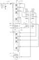
도 1을 참조하여, 본 발명의 바람직한 실시예에 따른 유도 결합 플라즈마 반응기는 병렬로 구성되는 제1 및 제2 플라즈마 반응기(10, 15), 제1 및 제2 플라즈마 반응기(10, 15)의 내부에 플라즈마 방전을 각기 유도하기 위한 제1 및 제2 용량 결합 전극 어셈블리(30, 35)를 구비한다. 제1 및 제2 용량 결합 전극 어셈블리(30, 35)의 사이에는 가스 공급부(20)가 구비된다. 제1 및 제2 플라즈마 반응기(10, 15)는 내부에 피처리 기판(13, 18)이 놓이는 지지대(12, 17)가 제1 및 제2 용량 결합 전극 어셈블리(30, 35)에 대향하여 일 측벽으로 설치된다. 가스 공급부(20)는 제1 및 제2 용량 결합 전극 어셈블리(30)의 사이에 구성되어 가스 공원(미도시)으로부터 제공된 가스를 제1 및 제2 용량 결합 전극 어셈블리(30, 35)의 가스 분사홀(32, 37)을 통하여 제1 및 제2 플라즈마 반응기(10, 15)의 내부로 공급한다. 메인 전원 공습원(40)으로부터 발생된 무선 주파수 전원은 임피던스 정합기(41)와 분배 회로(50)를 통하여 제1 및 제2 용량 결합 전극 어셈블리(30, 35)에 구비된 복수개의 용량 결합 전극(31, 33, 36, 38)으로 공급되어 제1 및 제2 플라즈마 반응기(10, 15)의 내부에 용량 결합된 플라즈마를 유도한다. 제1 및 제2 플라즈마 반응기(10, 15)의 내부에 발생된 플라즈마에 의해 피처리 기판(13, 18)에 대한 플라즈마 처리가 이루어진다.Referring to FIG. 1, an inductively coupled plasma reactor according to a preferred embodiment of the present invention includes the first and
제1 및 제2 플라즈마 반응기(10, 15)는 반응기 몸체(11, 16)와 그 내부에 피 처리 기판(13, 18)이 놓이는 지지대(12, 17)가 구비된다. 반응기 몸체(11, 16)는 알루미늄, 스테인리스, 구리와 같은 금속 물질로 재작될 수 있다. 또는 코팅된 금속 예를 들어, 양극 처리된 알루미늄이나 니켈 도금된 알루미늄으로 재작될 수도 있다. 또는 내화 금속(refractory metal)로 재작될 수도 있다. 또 다른 대안으로 반응기 몸체(11, 16)를 전체적 또는 부분적으로 석영, 세라믹과 같은 전기적 절연 물질로 재작하는 것도 가능하다. 이와 같이 반응기 몸체(11, 16)는 의도된 플라즈마 프로세스가 수행되기에 적합한 어떠한 물질로도 재작될 수 있다. 반응기 몸체(11, 16)의 구조는 피처리 기판(13, 18)에 따라 그리고 플라즈마의 균일한 발생을 위하여 적합한 구조 예를 들어, 원형 구조나 사각형 구조 그리고 이외에도 어떠한 형태의 구조를 가질 수 있다.The first and
피처리 기판(13, 18)은 예를 들어, 반도체 장치, 디스플레이 장치, 태양전지 등과 같은 다양한 장치들의 제조를 위한 웨이퍼 기판, 유리 기판, 플라스틱 기판 등과 같은 기판들이다. 제1 및 제2 플라즈마 반응기(10, 15)는 진공 펌프(미도시)에 연결된다. 하나의 진공 펌프를 사용하여 공통 배기 구조를 갖도록 하거나 또는 별개의 진공 펌프를 사용하여 각기 배기 구조를 갖도록 할 수 있다. 본 발명의 실시예에서 제1 및 제2 플라즈마 반응기(10, 15)는 대기압 이하의 저압 상태에서 피처리 기판(13, 18)에 대한 플라즈마 처리가 이루어진다. 그러나 본 발명의 용량 결합 플라즈마 반응기는 대기압에서 피처리 기판을 처리하는 대기압의 플라즈마 처리 시스템으로도 그 사용이 가능하다.The
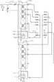
도 2는 용량 결합 전극 어셈블리와 가스 공급부를 보여주는 사시도이다.2 is a perspective view illustrating a capacitively coupled electrode assembly and a gas supply unit;
도 2를 참조하여, 가스 공급부(20)는 제1 및 제2 용량 결합 전극 어셈블리(30, 35)의 사이에 설치된다. 가스 공급부(20)는 가스 공급원(미도시)에 연결되는 복수개의 가스 공급관(21)을 포함한다. 복수개의 가스 공급관(21)은 각기 독립적으로 가스 공급 유량을 제어할 수 있는 조절 밸브(24)가 구비된다. 또는 복수개의 가스 공급관(21)에 대하여 일괄적으로 가스 공급 유량을 제어할 수 있도록 구성도 가능하다. 또는 복수개의 가스 공급관(21)에 대하여 전체적 및 개별적인 가스 공급 유량의 제어가 가능하도록 구성할 수도 있다.Referring to FIG. 2, the
복수개의 가스 공급관(21)은 복수개의 가스 주입구(22, 23)가 제1 및 제2 전극 장착판(34, 39)의 복수개의 가스 분사홀(32, 37)에 대응되어 연결된다. 가스 공급원으로부터 제공된 가스는 복수개의 가스 공급관(21)을 통하여 고르게 분배되어 복수개의 가스 주입구(22, 23)와 그에 대응된 복수개의 가스 분사홀(32, 37)을 통하여 제1 및 제2 플라즈마 반응기(10, 15)의 내부로 고르게 분사된다. 복수개의 가스 공급관(21)은 두 그룹으로 구분하여 분리된 가스 공급 채널을 구성하도록 할 수도 있다. 서로 다른 가스를 분리 공급하도록 하여 플라즈마 처리의 균일도를 높일 수 있다.In the plurality of
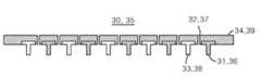
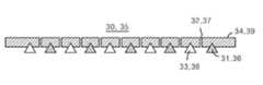
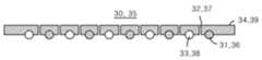
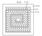
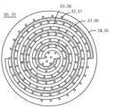
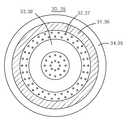
제1 및 제2 용량 결합 전극 어셈블리(30, 35)는 제1 및 제2 플라즈마 반응기(10, 15)의 내부에 용량 결합된 플라즈마 방전을 유도하기 위한 복수개의 용량 결합 전극(31, 33, 36, 38)을 구비한다. 복수개의 용량 결합 전극(31, 33, 36, 38)은 각각의 전극 장착판(34, 39)에 장착된다. 전극 장착판(34, 38)은 제1 및 제2 플라즈마 반응기(10, 15)의 지지대(12, 17)에 대향하며, 복수개의 용량 결합 전 극(31, 33, 36, 38)은 수평 또는 수직으로 배열되어 전극 장착판(34, 39)에 설치된다. 복수개의 용량 결합 전극(31, 33, 36, 38)은 복수개의 정전압 전극(33, 38)과 부전압 전극(31, 36)이 교대적으로 병렬로 배열된 구조를 갖는다. 복수개의 용량 결합 전극(31, 33)은 전극 장착판(34)에서 돌출된 선형의 장벽구조를 갖는다. 복수개의 용량 결합 전극(31, 33, 36, 38)은, 도 3에 도시된 바와 같이, 전도체 영역(71)과 그 외부를 감싸는 절연체 영역(71)으로 구성될 수 있다. 또는 전도체 영역(71)만을 구비할 수도 있다. 복수개의 용량 결합 전극(31, 33, 36, 38)의 형상과 배치 구조는 후술되는 바와 같이 다양한 변형이 가능하다.The first and second capacitively coupled
전극 장착판(34, 39)은 복수개의 가스 분사홀(32, 37)을 구비한다. 복수개의 가스 분사홀(32, 37)은 복수개의 용량 결합 전극(31, 33, 36, 38) 사이에 일정 간격을 두고 구성된다. 전극 장착판(34, 39)은 금속이나 비금속 또는 이들의 혼합된 물질로도 구성이 가능하다. 물론, 전극 장착판(34, 39)이 금속 물질로 구성되는 경우에는 복수개의 용량 결합 전극(31, 33, 36, 38)과의 사이에 전기적 절연 구조를 갖는다. 전극 장착판(34, 39)은 반응기 몸체(11, 16)의 일 측벽을 구성하도록 설치되지만 플라즈마 처리 효율을 높이기 위하여 반응기 몸체(11, 16)의 천정과 바닥 양측 벽면을 따라서 설치될 수도 있다. 또는 반응기 몸체(11, 16)의 일 측벽과 반응기 몸체(11, 16)의 천정과 바닥 양측 벽면을 따라서 모두 설치될 수도 있다. 구체적인 도시는 생략되었으나, 전극 장착판(34, 39)은 적절한 온도 제어를 위한 냉각 채널 또는 히팅 채널을 구비할 수 있다.The
도 4 내지 도 10은 용량 결합 전극의 다양한 변형들을 보여주는 용량 결합 전극 어셈블리의 단면도이다.4 through 10 are cross-sectional views of the capacitively coupled electrode assembly showing various modifications of the capacitively coupled electrode.
먼저, 도 4에 도시된 바와 같이, 용량 결합 전극(31, 33, 36, 38)은 장벽 구조를 갖되, 그 단면이 'T'형 구조를 가질 수 있으며, 그 머리 부분이 전극 장착판(34)에 고정되도록 설치되거나 그 반대의 배치 위치를 갖도록 설치될 수 있다. 용량 결합 전극(31, 33, 36, 38)은, 도 5에 도시된 바와 같이, 좁은 폭을 갖는 판형 구조를 가질 수 있다. 도 6 또는 도 7에 도시된 바와 같이, 용량 결합 전극(31, 33, 36, 38)은 그 단면 구조가 삼각 또는 역삼각 구조를 갖도록 할 수도 있다. 또는 도 8 내지 도 10에 도시된 바와 같이, 원통의 봉형 구조, 뉘어진 타원 구조나 세워진 타원 구조의 봉형 구조를 가질 수 있다. 이와 같이, 용량 결합 전극(31, 33, 36, 38)은 그 단면 구조가 원형, 타원형, 다각형 구조 등과 같이 다양한 구조를 가질 수 있다.First, as shown in FIG. 4, the
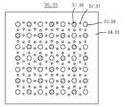
도 11 내지 도 21은 용량 결합 전극의 평면 구조 및 평면 배열 구조의 다양한 변형들을 보여주는 용량 결합 전극 어셈블리의 하부 평면도이다.11 to 21 are bottom plan views of capacitively coupled electrode assemblies showing various modifications of the planar structure and the planar arrangement of the capacitively coupled electrodes.
먼저, 도 11에 도시된 바와 같이, 복수개의 용량 결합 전극(31, 33, 36, 38)을 구성하는 복수개의 정전압 전극(33, 38)과 복수개의 부전압 전극(31, 36)은 상호 교대적으로 배열되고 그 사이에는 복수개의 가스 분사홀(32, 37)이 배열될 수 있다. 도 12 또는 도 13과 같이, 복수개의 정전압 전극(33, 38)과 부전압 전극(31, 36)은 일정 길이로 나뉜 구조에서 같은 전극이 동일 열(또는 행)로 배열되되 상호 교대적으로 배열된 구조(도 12) 또는 매트릭스형으로 배열된 구조(도 13)를 가질 수 있다. 도 14 또는 도 15에 도시된 바와 같이, 복수개의 용량 결합 전 극(31, 33, 36, 38)은 복수개의 사각 또는 원형의 평판형 면적극으로 구성될 수 있다. 도 16에 도시된 바와 같이, 복수개의 용량 결합 전극(31, 33, 36, 38)은 원기둥과 같은 기둥 구조를 가질 수도 있다. 도 17 내지 도 21에 도시된 바와 같이, 복수개의 용량 결합 전극(31, 33, 36, 38)은 상호 교대적으로 배열된 평판 나선형 구조나 동심원 구조를 가질 수 있다. 이러한 구조에서 복수개의 용량 결합 전극(31, 33, 36, 38)은 단지 하나의 정전압 전극(33, 38)과 부전압 전극(31, 36)으로 구성될 수도 있다.First, as shown in FIG. 11, the plurality of
이상과 같이, 복수개의 용량 결합 전극(31, 33, 36, 38)은 장벽 구조, 평판형 구조, 돌기형 구조, 기둥 구조, 동심원 또는 환형 구조, 나선형 구조, 선형 구조에서 선택된 하나 이상의 구조를 갖질 수 있다. 그리고 복수개의 정전압 전극(33, 38)과 부전압 전극(31, 36)의 상호 배열 구조 또한 상호 교대적인 선형 배열 구조, 매트릭스 형태의 배열 구조, 상호 교대적인 나선형 배열 구조, 상호 교대적인 동심원 배열 구조와 같은 다양한 배열 구조에서 선택된 하나 이상의 배열 구조를 가질 수 있다. 그리고 도면에는 구체적으로 도시하지 않았으나, 상기 복수개의 용량 결합 전극들(31, 33, 36, 38) 사이에는 절연층이 구성될 수 있다.As described above, the plurality of capacitively coupled
다시, 도 1을 참조하여, 제1 및 제2 플라즈마 반응기(10, 15)의 내부에는 피처리 기판(13, 18)을 지지하기 위한 지지대(12, 17)가 구비된다. 기판 지지대(12, 17)는 바이어스 전원 공급원(42, 43, 45, 46)에 연결되어 바이어스 된다. 예를 들어, 서로 다른 무선 주파수 전원을 공급하는 두 개의 바이어스 전원 공급원(42, 43, 45, 46)이 임피던스 정합기(44, 47)를 통하여 기판 지지대(12, 17)에 전기적으 로 연결되어 바이어스 된다. 기판 지지대(12, 17)의 이중 바이어스 구조는 제1 및 제2 플라즈마 반응기(10, 15)의 내부에 플라즈마 발생을 용이하게 하고, 플라즈마 이온 에너지 조절을 더욱 개선시켜 공정 생산력을 향상 시킬 수 있다. 또는 단일 바이어스 구조로 변형 실시할 수도 있다. 또는 지지대(12, 17)는 바이어스 전원의 공급 없이 제로 퍼텐셜(zero potential)을 갖는 구조로 변형 실시될 수도 있다. 그리고 기판 지지대(12, 17)는 정전척을 포함할 수 있다. 또는 기판 지지대(12, 17)는 히터를 포함할 수 있다.Again, referring to FIG. 1, the
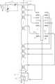
복수개의 용량 결합 전극(31, 33, 36, 38)은 메인 전원 공급원(40)으로부터 발생된 무선 주파수 전원을 임피던스 정합기(41)와 분배 회로(50)를 통하여 공급받아 구동되어 제1 및 제2 플라즈마 반응기(10, 15) 내부의 용량 결합된 플라즈마를 유도한다. 메인 전원 공급원(40)은 별도의 임피던스 정합기 없이 출력 전원의 제어가 가능한 무선 주파수 발생기를 사용하여 구성될 수도 있다. 분배 회로(50)는 메인 전원 공급원(40)으로부터 제공되는 무선 주파수 전원을 복수개의 용량 결합 전극(31, 33, 36, 38)으로 분배하여 병렬 구동되게 한다. 바람직하게, 분배 회로(50)는 전류 균형 회로로 구성되어 복수개의 용량 결합 전극(31, 33, 36, 38)으로 공급되는 전류가 자동적으로 상호 균형을 이루게 된다. 본 발명의 용량 결합 플라즈마 반응기는 복수개의 용량 결합 전극(31, 33, 36, 38)에 의해 대면적의 플라즈마를 균일하게 발생할 수 있다. 또한, 복수개의 용량 결합 전극을 병렬 구동함에 있어서 전류 균형을 자동적으로 이루도록 함으로 대면적의 플라즈마를 보다 균일하게 발생 및 유지할 수 있다.The plurality of
도 22는 분배 회로를 전류 균형 회로로 구성한 일 예를 보여주는 도면이다.22 is a diagram illustrating an example in which a distribution circuit is configured as a current balancing circuit.
도 22를 참조하여, 분배 회로(50)는 복수개의 용량 결합 전극(31, 33, 36, 38)을 병렬 구동하며 전류 균형을 이루는 복수개의 트랜스포머(52)를 포함한다. 복수개의 트랜스포머(52)의 일차측은 무선 주파수가 입력되는 전원 입력단과 접지 사이에 직렬로 연결되며, 이차측의 일단은 복수개의 용량 결합 전극(31, 33, 36, 38)에 대응되게 연결되고 타단은 공통으로 접지된다. 복수개의 트랜스포머(52)는 전원 입력단과 접지 사이의 전압을 균등하게 분할하고 분할된 다수의 분할된 전압을 복수개의 용량 결합 전극(31, 33, 36, 38) 중에서 대응된 정전압 전극(33, 38)으로 출력한다. 복수개의 용량 결합 전극(31, 33, 36, 38) 중에서 부전압 전극(31, 36)은 공통으로 접지된다.Referring to FIG. 22, the
복수개의 트랜스포머(52)의 일차측으로 흐르는 전류는 동일함으로 복수개의 정전압 전극(33, 38)으로 공급되는 전력도 동일하게 된다. 복수개의 용량 결합 전극(31, 33, 36, 38)들 중에서 어느 하나의 임피던스가 변화되어 전류량의 변화가 발생되면 복수개의 트랜스포머(52)가 전체적으로 상호 작용하여 전류 균형을 이루게 된다. 그럼으로 복수개의 용량 결합 전극(31, 33, 36, 38)으로 공급되는 전류는 상호 균일하게 지속적인 자동 조절이 이루어진다. 복수개의 트랜스포머(52)는 각기 일차측과 이차측의 권선비율이 기본적으로 1:1로 설정되어 있으나 이는 변경이 가능하다.Since the current flowing to the primary side of the plurality of
이상과 같은 전류 균형 회로(50)는, 도면에는 구체적인 도시를 생략하였으나, 복수개의 트랜스포머(52)에 과도전압이 발생되는 것을 방지하기 위한 보호 회 로를 포함할 수 있다. 보호 회로는 복수개의 트랜스포머(52) 중 어느 하나가 전기적으로 오픈 상태로 되어 해당 트랜스포머에 과도전압이 증가되는 것을 방지한다. 이러한 기능의 보호 회로는 바람직하게는 복수개의 트랜스포머(52)의 각각의 일차측 양단에 배리스터(Varistor)를 연결하여 구현할 수 있으며, 또는 제너다이오드(Zener Diode)와 같은 정전압 다이오드를 사용하여 구현할 수 있다. 그리고 전류 균형 회로(50)에는 각각의 트랜스포머(52) 마다 누설 전류의 보상을 위한 보상 커패시터(51)와 같은 보상 회로가 부가될 수 있다.Although the
도 23 내지 도 28은 분배 회로의 다양한 변형들을 보여주는 도면이다.23 to 28 show various modifications of the distribution circuit.
도 23을 참조하여, 일 변형의 전류 균형 회로(50)는 복수개의 트랜스포머(52)의 이차측들이 각기 접지된 중간 탭을 포함하여 이차측의 일단은 정전압을 타단은 부전압을 각각 출력한다. 정전압은 복수개의 용량 결합 전극의 정전압 전극(33, 38)으로 부전압은 복수개의 용량 결합 전극의 부전압 전극(31, 36)으로 제공된다.Referring to FIG. 23, one variation of the
도 24를 참조하여, 또 다른 변형의 전류 균형 회로(50a, 50b)는 분리된 제1 및 제2 전류 균형 회로(50a, 50b)로 구성될 수도 있다. 제1 및 제2 전류 균형 회로(50a, 50b) 임피던스 정합기(41)에 병렬로 연결된다. 제1 전류 균형 회로(50a)는 제1 용량 결합 전극 어셈블리(30)의 복수개의 용량 결합 전극(31, 33)에 그리고 제2 전류 균형 회로(50b)는 제2 용량 결합 전극 어셈블리(35)의 복수개의 용량 결합 전극(36, 38)에 각기 대응되어 구성된다.Referring to FIG. 24, another variation of the
도 25 및 도 26을 참조하여, 다른 변형의 전류 규형 회로(50)는 전류 균형 조절 범위를 가변 할 수 있는 전압 레벨 조절 회로(60)를 구비할 수 있다. 전압 레벨 조절 회로(60)는 멀티 탭을 구비한 코일(61)과 멀티 탭 중 어느 하나를 접지로 연결하는 멀티 탭 스위칭 회로(62)를 포함한다. 전압 레벨 조절 회로(60)는 멀티 탭 스위칭 회로(62)의 스위칭 위치에 따라 가변된 전압 레벨을 전류 균형 회로(50)로 인가하게 되며, 전류 균형 회로(50)는 전압 레벨 조절 회로(60)에 의해서 결정되는 전압 레벨에 의해 전류 균형 조절 범위가 가변된다. 그리고 도 27 및 도 28에 도시된 바와 같이, 제1 및 제2 전류 균형 회로(50a, 50b)로 구성된 경우에도 역시 동일하게 각기 전압 레벨 조절 회로(60a, 60b)가 구비될 수 있다.25 and 26, another variation of the
이상에서 설명된 본 발명의 용량 결합 플라즈마 반응기의 실시예는 예시적인 것에 불과하며, 본 발명이 속한 기술분야의 통상의 지식을 가진 자라면 이로부터 다양한 변형 및 균등한 타 실시예가 가능하다는 점을 잘 알 수 있을 것이다. 그럼으로 본 발명은 상기의 상세한 설명에서 언급되는 형태로만 한정되는 것은 아님을 잘 이해할 수 있을 것이다. 따라서 본 발명의 진정한 기술적 보호 범위는 첨부된 특허청구범위의 기술적 사상에 의해 정해져야 할 것이다. 또한, 본 발명은 첨부된 청구범위에 의해 정의되는 본 발명의 정신과 그 범위 내에 있는 모든 변형물과 균등물 및 대체물을 포함하는 것으로 이해되어야 한다.The embodiment of the capacitively coupled plasma reactor of the present invention described above is merely illustrative, and it is well understood that various modifications and equivalent other embodiments are possible to those skilled in the art to which the present invention pertains. You will know. Therefore, it will be understood that the present invention is not limited only to the form mentioned in the above detailed description. Therefore, the true technical protection scope of the present invention will be defined by the technical spirit of the appended claims. It is also to be understood that the present invention includes all modifications, equivalents, and substitutes within the spirit and scope of the invention as defined by the appended claims.
본 발명의 용량 결합 플라즈마 반응기는 반도체 집적 회로의 제조, 평판 디스플레이 제조, 태양전지의 제조와 같은 다양한 박막 형성을 위한 플라즈마 처리 공정에 매우 유용하게 이용될 수 있다. 특히, 본 발명의 용량 결합 플라즈마 반응 기는 복수개의 용량 결합 전극에 의해 대면적의 플라즈마를 균일하게 발생할 수 있다. 또한, 복수개의 용량 결합 전극을 병렬 구동함에 있어서 전류 균형을 자동적으로 이루도록 함으로 대면적의 플라즈마를 보다 균일하게 발생 및 유지할 수 있다. The capacitively coupled plasma reactor of the present invention can be very usefully used in plasma processing processes for forming various thin films, such as the manufacture of semiconductor integrated circuits, the manufacture of flat panel displays, and the manufacture of solar cells. In particular, the capacitively coupled plasma reactor of the present invention can generate a large area of plasma uniformly by a plurality of capacitively coupled electrodes. In addition, it is possible to generate and maintain the plasma of a large area more uniformly by automatically balancing the currents in parallel driving the plurality of capacitive coupling electrodes.
도 1은 본 발명의 바람직한 실시예예 따른 플라즈마 반응기의 단면도이다.1 is a cross-sectional view of a plasma reactor according to a preferred embodiment of the present invention.
도 2는 용량 결합 전극 어셈블리와 가스 공급부를 보여주는 사시도이다.2 is a perspective view illustrating a capacitively coupled electrode assembly and a gas supply unit;
도 3은 용량 결합 전극의 단면도이다.3 is a cross-sectional view of the capacitive coupling electrode.
도 4 내지 도 10은 용량 결합 전극의 다양한 변형들을 보여주는 용량 결합 전극 어셈블리의 단면도이다.4 through 10 are cross-sectional views of the capacitively coupled electrode assembly showing various modifications of the capacitively coupled electrode.
도 11 내지 도 21은 용량 결합 전극의 평면 구조 및 평면 배열 구조의 다양한 변형들을 보여주는 용량 결합 전극 어셈블리의 하부 평면도이다.11 to 21 are bottom plan views of capacitively coupled electrode assemblies showing various modifications of the planar structure and the planar arrangement of the capacitively coupled electrodes.
도 22는 분배 회로를 전류 균형 회로로 구성한 일 예를 보여주는 도면이다.22 is a diagram illustrating an example in which a distribution circuit is configured as a current balancing circuit.
도 23 내지 도 28은 분배 회로의 다양한 변형들을 보여주는 도면이다.23 to 28 show various modifications of the distribution circuit.
*도면의 주요 부분에 대한 부호의 설명** Description of the symbols for the main parts of the drawings *
8: 진공 펌프10: 플라즈마 반응기8: vacuum pump 10: plasma reactor
11: 반응기 몸체12: 지지대11: reactor body 12: support
13: 피처리 기판20: 가스 공급부13: substrate to be processed 20: gas supply part
21: 가스 입구22: 가스 분배판21: gas inlet 22: gas distribution plate
23: 가스 주입구30: 용량 결합 전극 어셈블리23: gas inlet 30: capacitive coupling electrode assembly
31, 33: 용량 결합 전극32: 가스 분사홀31, 33: capacitive coupling electrode 32: gas injection hole
34: 전극 장착판40: 메인 전원 공급원34: electrode mounting plate 40: main power supply
41: 임피던스 정합기42, 43: 바이어스 전원 공급원41:
44: 임피던스 정합기50: 분배 회로44: impedance matcher 50: distribution circuit
51: 보상 커패시터52: 트랜스포머51: compensation capacitor 52: transformer
53: 중간탭60: 전압 레벨 조절 회로53: middle tap 60: voltage level adjustment circuit
61: 코일62: 멀티 탭 스위칭 회로61: coil 62: multi-tap switching circuit
70: 절연체 영역71: 전도체 영역70: insulator region 71: conductor region
Claims (21)
Translated fromKoreanPriority Applications (7)
| Application Number | Priority Date | Filing Date | Title |
|---|---|---|---|
| KR1020070106349AKR100955207B1 (en) | 2007-10-22 | 2007-10-22 | Capacitively Coupled Plasma Reactor for Dual-Substrate Processing |
| TW097115723ATWI440405B (en) | 2007-10-22 | 2008-04-29 | Capacitively coupled plasma reactor |
| US12/114,879US8018163B2 (en) | 2007-10-22 | 2008-05-05 | Capacitively coupled plasma reactor |
| JP2008125624AJP5668957B2 (en) | 2007-10-22 | 2008-05-13 | Capacitively coupled plasma reactor |
| CN200810108452.6ACN101420816B (en) | 2007-10-22 | 2008-05-30 | Capacitively coupled plasma reactor |
| EP08167240AEP2053630A3 (en) | 2007-10-22 | 2008-10-22 | Capacitively coupled plasma reactor |
| PCT/KR2008/006241WO2009054671A2 (en) | 2007-10-22 | 2008-10-22 | Capacitively coupled plasma reactor |
Applications Claiming Priority (1)
| Application Number | Priority Date | Filing Date | Title |
|---|---|---|---|
| KR1020070106349AKR100955207B1 (en) | 2007-10-22 | 2007-10-22 | Capacitively Coupled Plasma Reactor for Dual-Substrate Processing |
Publications (2)
| Publication Number | Publication Date |
|---|---|
| KR20090040819A KR20090040819A (en) | 2009-04-27 |
| KR100955207B1true KR100955207B1 (en) | 2010-04-29 |
Family
ID=40764106
Family Applications (1)
| Application Number | Title | Priority Date | Filing Date |
|---|---|---|---|
| KR1020070106349AExpired - Fee RelatedKR100955207B1 (en) | 2007-10-22 | 2007-10-22 | Capacitively Coupled Plasma Reactor for Dual-Substrate Processing |
Country Status (1)
| Country | Link |
|---|---|
| KR (1) | KR100955207B1 (en) |
Families Citing this family (2)
| Publication number | Priority date | Publication date | Assignee | Title |
|---|---|---|---|---|
| KR101585890B1 (en)* | 2009-05-31 | 2016-01-15 | 위순임 | Large Area Plasma Reactor Consisting of Vertical Dual Chambers |
| KR102020826B1 (en)* | 2018-12-03 | 2019-09-11 | 주성엔지니어링(주) | Plasma Genearation Apparatus And Plasma Generation Method |
Citations (4)
| Publication number | Priority date | Publication date | Assignee | Title |
|---|---|---|---|---|
| JP2000331995A (en) | 1999-05-19 | 2000-11-30 | Anelva Corp | Flat plate type gas introduction device for CCP reaction vessel |
| KR100302167B1 (en) | 1993-11-05 | 2001-11-22 | 히가시 데쓰로 | Plasma Treatment Equipment and Plasma Treatment Methods |
| KR20060128303A (en)* | 2005-06-10 | 2006-12-14 | 주식회사 뉴파워 프라즈마 | Plasma processing unit equipped with a capacitively coupled plasma source and a vertical dual process chamber |
| KR20070101067A (en)* | 2006-04-11 | 2007-10-16 | 주식회사 뉴파워 프라즈마 | Complex Plasma Source and Gas Separation Method Using the Same |
- 2007
- 2007-10-22KRKR1020070106349Apatent/KR100955207B1/ennot_activeExpired - Fee Related
Patent Citations (4)
| Publication number | Priority date | Publication date | Assignee | Title |
|---|---|---|---|---|
| KR100302167B1 (en) | 1993-11-05 | 2001-11-22 | 히가시 데쓰로 | Plasma Treatment Equipment and Plasma Treatment Methods |
| JP2000331995A (en) | 1999-05-19 | 2000-11-30 | Anelva Corp | Flat plate type gas introduction device for CCP reaction vessel |
| KR20060128303A (en)* | 2005-06-10 | 2006-12-14 | 주식회사 뉴파워 프라즈마 | Plasma processing unit equipped with a capacitively coupled plasma source and a vertical dual process chamber |
| KR20070101067A (en)* | 2006-04-11 | 2007-10-16 | 주식회사 뉴파워 프라즈마 | Complex Plasma Source and Gas Separation Method Using the Same |
Also Published As
| Publication number | Publication date |
|---|---|
| KR20090040819A (en) | 2009-04-27 |
Similar Documents
| Publication | Publication Date | Title |
|---|---|---|
| JP5668957B2 (en) | Capacitively coupled plasma reactor | |
| KR100979186B1 (en) | Capacitively coupled plasma reactor | |
| KR100979189B1 (en) | Continuous substrate processing system | |
| KR101160906B1 (en) | Capacitively coupled plasma reactor | |
| KR101463934B1 (en) | Compound plasma reactor | |
| KR101167952B1 (en) | Plasma reactor for generating large size plasma | |
| KR100955207B1 (en) | Capacitively Coupled Plasma Reactor for Dual-Substrate Processing | |
| KR100963848B1 (en) | Capacitively Coupled Plasma Reactor with Multi-Laser Scanning Line | |
| KR20100129373A (en) | Hybrid Plasma Reactor | |
| KR101507390B1 (en) | Capacitively coupled plasma reactor | |
| KR100980281B1 (en) | Dual Plasma Reactor with Multi-Core Plasma Generator | |
| KR100979188B1 (en) | Physical Vapor Deposition Plasma Reactor with Multi-Source Target Assembly | |
| KR101626043B1 (en) | Multiplex frequency driven capacitively coupled plasma reactor | |
| KR101609319B1 (en) | Compound plasma reactor | |
| KR100979187B1 (en) | Dual Plasma Reactor for Dual Substrate Processing with Multi Laser Scanning Lines | |
| KR100983556B1 (en) | Plasma reactor having multi-core plasma generator | |
| KR101533710B1 (en) | An internal plasma reactor having a multi-frequency driven capacitive coupling electrode assembly | |
| KR101139824B1 (en) | Plasma reactor for generating large size plasma | |
| KR101534815B1 (en) | A capacitively coupled plasma reactor having a multi-frequency driven capacitive coupling electrode assembly, a plasma processing method using the same, and a device manufactured thereby | |
| KR20110054456A (en) | Capacitively coupled plasma reactor | |
| KR20090069799A (en) | Multiple Inductively Coupled Dual Plasma Reactors with Multiple Laser Scanning Lines | |
| KR20100100226A (en) | Compound plasma reactor | |
| KR20090069347A (en) | Multi-loop core dual plasma reactor with multiple laser scanning lines | |
| KR20090116562A (en) | Mixed Plasma Reactor |
Legal Events
| Date | Code | Title | Description |
|---|---|---|---|
| PA0109 | Patent application | St.27 status event code:A-0-1-A10-A12-nap-PA0109 | |
| P11-X000 | Amendment of application requested | St.27 status event code:A-2-2-P10-P11-nap-X000 | |
| P13-X000 | Application amended | St.27 status event code:A-2-2-P10-P13-nap-X000 | |
| A201 | Request for examination | ||
| PA0201 | Request for examination | St.27 status event code:A-1-2-D10-D11-exm-PA0201 | |
| N231 | Notification of change of applicant | ||
| PN2301 | Change of applicant | St.27 status event code:A-3-3-R10-R13-asn-PN2301 St.27 status event code:A-3-3-R10-R11-asn-PN2301 | |
| PG1501 | Laying open of application | St.27 status event code:A-1-1-Q10-Q12-nap-PG1501 | |
| N231 | Notification of change of applicant | ||
| PN2301 | Change of applicant | St.27 status event code:A-3-3-R10-R13-asn-PN2301 St.27 status event code:A-3-3-R10-R11-asn-PN2301 | |
| D13-X000 | Search requested | St.27 status event code:A-1-2-D10-D13-srh-X000 | |
| D14-X000 | Search report completed | St.27 status event code:A-1-2-D10-D14-srh-X000 | |
| E701 | Decision to grant or registration of patent right | ||
| PE0701 | Decision of registration | St.27 status event code:A-1-2-D10-D22-exm-PE0701 | |
| GRNT | Written decision to grant | ||
| PR0701 | Registration of establishment | St.27 status event code:A-2-4-F10-F11-exm-PR0701 | |
| PR1002 | Payment of registration fee | St.27 status event code:A-2-2-U10-U11-oth-PR1002 Fee payment year number:1 | |
| PG1601 | Publication of registration | St.27 status event code:A-4-4-Q10-Q13-nap-PG1601 | |
| R17-X000 | Change to representative recorded | St.27 status event code:A-5-5-R10-R17-oth-X000 | |
| FPAY | Annual fee payment | Payment date:20130422 Year of fee payment:4 | |
| PR1001 | Payment of annual fee | St.27 status event code:A-4-4-U10-U11-oth-PR1001 Fee payment year number:4 | |
| PN2301 | Change of applicant | St.27 status event code:A-5-5-R10-R11-asn-PN2301 | |
| PN2301 | Change of applicant | St.27 status event code:A-5-5-R10-R14-asn-PN2301 | |
| P14-X000 | Amendment of ip right document requested | St.27 status event code:A-5-5-P10-P14-nap-X000 | |
| P16-X000 | Ip right document amended | St.27 status event code:A-5-5-P10-P16-nap-X000 | |
| Q16-X000 | A copy of ip right certificate issued | St.27 status event code:A-4-4-Q10-Q16-nap-X000 | |
| L13-X000 | Limitation or reissue of ip right requested | St.27 status event code:A-2-3-L10-L13-lim-X000 | |
| U15-X000 | Partial renewal or maintenance fee paid modifying the ip right scope | St.27 status event code:A-4-4-U10-U15-oth-X000 | |
| FPAY | Annual fee payment | Payment date:20140421 Year of fee payment:5 | |
| PR1001 | Payment of annual fee | St.27 status event code:A-4-4-U10-U11-oth-PR1001 Fee payment year number:5 | |
| PN2301 | Change of applicant | St.27 status event code:A-5-5-R10-R11-asn-PN2301 | |
| PN2301 | Change of applicant | St.27 status event code:A-5-5-R10-R14-asn-PN2301 | |
| PC1903 | Unpaid annual fee | St.27 status event code:A-4-4-U10-U13-oth-PC1903 Not in force date:20150422 Payment event data comment text:Termination Category : DEFAULT_OF_REGISTRATION_FEE | |
| K11-X000 | Ip right revival requested | St.27 status event code:A-6-4-K10-K11-oth-X000 | |
| PC1903 | Unpaid annual fee | St.27 status event code:N-4-6-H10-H13-oth-PC1903 Ip right cessation event data comment text:Termination Category : DEFAULT_OF_REGISTRATION_FEE Not in force date:20150422 | |
| PN2301 | Change of applicant | St.27 status event code:A-5-5-R10-R11-asn-PN2301 | |
| PR0401 | Registration of restoration | St.27 status event code:A-6-4-K10-K13-oth-PR0401 | |
| PR1001 | Payment of annual fee | St.27 status event code:A-4-4-U10-U11-oth-PR1001 Fee payment year number:6 | |
| PN2301 | Change of applicant | St.27 status event code:A-5-5-R10-R14-asn-PN2301 | |
| LAPS | Lapse due to unpaid annual fee | ||
| PC1903 | Unpaid annual fee | St.27 status event code:A-4-4-U10-U13-oth-PC1903 Not in force date:20160422 Payment event data comment text:Termination Category : DEFAULT_OF_REGISTRATION_FEE | |
| P22-X000 | Classification modified | St.27 status event code:A-4-4-P10-P22-nap-X000 | |
| PC1903 | Unpaid annual fee | St.27 status event code:N-4-6-H10-H13-oth-PC1903 Ip right cessation event data comment text:Termination Category : DEFAULT_OF_REGISTRATION_FEE Not in force date:20160422 |